CN102290440A - Transistor and method of manufacturing the same - Google Patents
Transistor and method of manufacturing the sameDownload PDFInfo
- Publication number
- CN102290440A CN102290440ACN2010102092387ACN201010209238ACN102290440ACN 102290440 ACN102290440 ACN 102290440ACN 2010102092387 ACN2010102092387 ACN 2010102092387ACN 201010209238 ACN201010209238 ACN 201010209238ACN 102290440 ACN102290440 ACN 102290440A
- Authority
- CN
- China
- Prior art keywords
- active layer
- layer
- transistor
- drain
- dielectric layer
- Prior art date
- Legal status (The legal status is an assumption and is not a legal conclusion. Google has not performed a legal analysis and makes no representation as to the accuracy of the status listed.)
- Pending
Links
Images


Landscapes
- Thin Film Transistor (AREA)
Abstract
Description
Translated fromChinese技术领域technical field
本发明涉及一种晶体管及其制造方法。The invention relates to a transistor and its manufacturing method.
背景技术Background technique
氧化物晶体管元件具有优异的元件特性、极佳的均匀性以及适用于大面积且低温工艺的特性,使得各个厂商纷纷投入该领域的研发,然而氧化物晶体管虽然具有优异的元件特性,但因为材料系统的关系,容易受到外界环境以及工艺所影响,一般常见的在于反交叠型(Inverted stagger)结构或是共平面(coplanar)型结构的氧化物晶体管元件的源极与漏极在制作时,因电极蚀刻时同时对于沟道也会造成伤害,使得元件稳定性不佳。一般常见的解决方法是在源极与漏极的导电层沉积之前,在有源层的表面上先覆盖一层沟道保护层(channel protection layer),如美国专利第6653159号,以保护有源层,避免其遭受蚀刻的破坏。另一种方法,则是在源极与漏极蚀刻之后透过弱酸将有源层表面受损的区域移除。Oxide transistors have excellent device characteristics, excellent uniformity, and are suitable for large-area and low-temperature processes, so that various manufacturers have invested in research and development in this field. However, although oxide transistors have excellent device characteristics, due to the material The relationship between the system is easily affected by the external environment and process. It is generally common that the source and drain of oxide transistor elements with an inverted stagger structure or a coplanar structure are produced. Because the channel is also damaged when the electrode is etched, the stability of the device is not good. A common solution is to cover the surface of the active layer with a channel protection layer (channel protection layer) before the conductive layer of the source and drain is deposited, such as U.S. Patent No. 6,653,159 to protect the active layer. layer to prevent it from being damaged by etching. Another method is to remove the damaged area on the surface of the active layer with a weak acid after the source and drain etch.
发明内容Contents of the invention
本发明提出一种晶体管,包括栅极、有源层堆叠结构、介电层以及源极与漏极。栅极位于介电层的上述第一表面上。有源层堆叠结构包括第一有源层与第二有源层,位于介电层的第二表面上。源极与漏极位于介电层的第二表面上,且分别位于有源层堆叠结构两侧,并分别延伸至有源层堆叠结构的第一有源层与第二有源层之间。The invention provides a transistor, which includes a gate, an active layer stack structure, a dielectric layer, and a source and a drain. The gate is located on the first surface of the dielectric layer. The active layer stack structure includes a first active layer and a second active layer located on the second surface of the dielectric layer. The source and the drain are located on the second surface of the dielectric layer, are respectively located on two sides of the active layer stack structure, and respectively extend between the first active layer and the second active layer of the active layer stack structure.
本发明再提出一种晶体管的制造方法,包括于基板上形成栅极,接着,在栅极与基板上形成介电层。于介电层上形成有源层堆叠结构的第一有源层。于第一有源层与介电层上形成源极与漏极,分别覆盖上述第一有源层两侧,其中在源极与漏极之间具有间隙,露出第一有源层。于间隙中以及部分上述源极与上述漏极上形成有源层堆叠结构的第二有源层。The present invention further proposes a method for manufacturing a transistor, which includes forming a gate on a substrate, and then forming a dielectric layer on the gate and the substrate. The first active layer of the active layer stack structure is formed on the dielectric layer. A source and a drain are formed on the first active layer and the dielectric layer, covering both sides of the first active layer respectively, wherein there is a gap between the source and the drain to expose the first active layer. A second active layer of an active layer stack structure is formed in the gap and on part of the source and the drain.
本发明又提出一种晶体管的制造方法,包括于基板上形成有源层堆叠结构的第一有源层,在第一有源层与基板上形成源极与漏极分别覆盖第一有源层两侧,其中源极与漏极之间具有间隙,暴露出第一有源层。于间隙以及部分源极与漏极上形成有源层堆叠结构的第二有源层。于源极、漏极、第二有源层与基板上形成介电层。于介电层上形成栅极。The present invention further proposes a method for manufacturing a transistor, which includes forming a first active layer with an active layer stack structure on a substrate, and forming a source electrode and a drain electrode on the first active layer and the substrate to cover the first active layer respectively. On both sides, there is a gap between the source and the drain, exposing the first active layer. A second active layer of the active layer stack structure is formed on the gap and part of the source and drain. A dielectric layer is formed on the source electrode, the drain electrode, the second active layer and the substrate. A gate is formed on the dielectric layer.
为让本发明的上述特征能更明显易懂,下文特举实施例,并配合附图作详细说明如下。In order to make the above-mentioned features of the present invention more comprehensible, the following specific embodiments are described in detail with accompanying drawings.
附图说明Description of drawings
图1A至1E是依照本发明实施例所绘示的一种具有反交叠型结构的半导体氧化物晶体管的有源矩阵有机发光二极管显示器的制造方法流程剖面示意图。FIGS. 1A to 1E are schematic cross-sectional views of a manufacturing method of an active matrix organic light emitting diode display having semiconductor oxide transistors with an inverted overlap structure according to an embodiment of the present invention.
图2A至2C是依照本发明实施例所绘示的一种反交叠型结构的半导体氧化物晶体管的制造方法流程剖面示意图。2A to 2C are schematic cross-sectional views of a method for manufacturing a semiconductor oxide transistor with an inverted overlap structure according to an embodiment of the present invention.
图3A至3C是依照本发明实施例所绘示的另一种反交叠型结构的半导体氧化物晶体管的制造方法流程剖面示意图。3A to 3C are schematic cross-sectional views of another method for manufacturing a semiconductor oxide transistor with an inverted overlap structure according to an embodiment of the present invention.
图4A至4C是依照本发明实施例所绘示的一种共平面结构型的半导体氧化物晶体管的制造方法流程剖面示意图。4A to 4C are cross-sectional schematic diagrams illustrating a manufacturing method of a coplanar semiconductor oxide transistor according to an embodiment of the present invention.
图5A至5C是依照本发明实施例所绘示的另一种共平面结构型的半导体氧化物晶体管的制造方法流程剖面示意图。5A to 5C are cross-sectional schematic diagrams illustrating the process flow of another method for manufacturing a coplanar semiconductor oxide transistor according to an embodiment of the present invention.
图6A至6C是依照本发明实施例所绘示的另一种共平面结构型的半导体氧化物晶体管的制造方法流程剖面示意图。6A to 6C are cross-sectional schematic diagrams illustrating the process flow of another method for manufacturing a coplanar semiconductor oxide transistor according to an embodiment of the present invention.
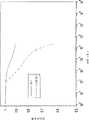
图7是本发明实验例1、比较例1、2、3的半导体氧化物晶体管在较大的饱和电流Id以及电压Vg(Id=80μA;Vg=20V)下进行测试的电性表现。7 is the electrical performance of the semiconductor oxide transistors of Experimental Example 1 and Comparative Examples 1, 2, and 3 of the present invention tested under a relatively large saturation current Id and voltage Vg (Id=80μA; Vg=20V).
图8是本发明实验例1与比较例1的半导体氧化物晶体管在一般条件(Id=6μA;Vg=10V)下进行测试的电性表现。FIG. 8 is the electrical performance of the semiconductor oxide transistors of Experimental Example 1 and Comparative Example 1 tested under general conditions (Id=6 μA; Vg=10V).
图9是本发明实验例1的半导体氧化物晶体管在施加应力(stress)前后的电性表现。FIG. 9 is the electrical performance of the semiconductor oxide transistor of Experimental Example 1 of the present invention before and after stress is applied.
图10为图1A至1C的反交叠型结构的半导体氧化物晶体管的制造方法流程图。FIG. 10 is a flow chart of a method for fabricating the semiconductor oxide transistor with the reverse overlap structure shown in FIGS. 1A to 1C .
图11为图4A至4C的反交叠型结构的半导体氧化物晶体管的制造方法流程图。FIG. 11 is a flow chart of a method for fabricating the semiconductor oxide transistor with the reverse overlap structure shown in FIGS. 4A to 4C .
附图标记说明Explanation of reference signs
10:基板10: Substrate
20:栅极20: grid
30:介电层30: Dielectric layer
30a、30b、62c:表面30a, 30b, 62c: surface
40:源极40: source
50:漏极50: drain
60:有源层堆叠结构60: active layer stack structure
62、64:有源层62, 64: active layer
62a、62b:部分62a, 62b: part
62d:侧壁62d: side wall
66、68:间隙66, 68: Clearance
64a、64b:延伸部64a, 64b: Extensions
70:沟道70: channel
80:保护层80: protective layer
88、90:表面处理88, 90: surface treatment
92:接触窗92: contact window
100a~100f:半导体氧化物晶体管100a to 100f: semiconductor oxide transistors
102:接触窗开口102: contact window opening
104、110:电极层104, 110: electrode layer
106:绝缘层106: insulation layer
108:有机发光层108: Organic light-emitting layer
120~170、220~270:步骤120~170, 220~270: steps
具体实施方式Detailed ways
图1A至1E是依照本发明实施例所绘示的一种具有反交叠型(InvertedStagger)结构的半导体氧化物晶体管的有源矩阵有机发光二极管(ActiveMatrix Organic Light Emitting Diode,AMOLED)显示器的制造方法流程剖面示意图。图10为图1A至1C的反交叠型结构的半导体氧化物晶体管的制造方法流程图。1A to 1E are a method of manufacturing an active matrix organic light emitting diode (ActiveMatrix Organic Light Emitting Diode, AMOLED) display with a semiconductor oxide transistor having an inverted stagger structure according to an embodiment of the present invention. Schematic diagram of the process section. FIG. 10 is a flow chart of a method for fabricating the semiconductor oxide transistor with the reverse overlap structure shown in FIGS. 1A to 1C .
请参照图1A与图10,进行步骤120,在基板10上形成栅极20。接着,进行步骤130,在栅极20与基板10上形成介电层30,再进行步骤140,在介电层30上形成第一有源层62。其后,进行步骤150,在第一有源层62上形成源极40以及漏极50。源极40以及漏极50彼此分隔且具有间隙66。需说明的是,源极40以及漏极50可互换。在一情况下,标记40所表示的构件作为源极;标记50所表示的构件作为漏极;而在另一情况下,标记40所表示的构件作为漏极;标记50所表示的构件作为源极。Referring to FIG. 1A and FIG. 10 ,
之后,进行步骤155,选择性进行表面处理工艺88,以使第一有源层62的组成配比更稳定。表面处理工艺88例如是等离子体工艺。等离子体工艺包括氢等离子体工艺、含氢离子等离子体工艺或含氧离子的等离子体工艺。Afterwards,
其后,请参照图1B与图10,进行步骤160,在基板10上形成第二有源层64。第二有源层64覆盖源极40以及漏极50并且填入于间隙66之中,与第一有源层62的上表面62c电性连接。第一有源层62与第二有源层64构成有源层堆叠结构60,第二有源层64中填入于间隙66之中的部分为第二有源层64的延伸部64a,其位于源极40以及漏极50之间,作为晶体管的沟道70。Thereafter, referring to FIG. 1B and FIG. 10 ,
之后,请参照图1C,进行步骤170,在基板10上形成保护层80,以覆盖基板10上的介电层30、源极40、漏极50以及有源层堆叠结构60,完成半导体氧化物晶体管100a、100b的制作。Afterwards, referring to FIG. 1C,
上述方法所形成的半导体氧化物晶体管100a、100b的栅极20位于介电层30的第一表面30a上,有源层堆叠结构60则位于介电层30的第二表面30b上。有源层堆叠结构60包括第一有源层62与第二有源层64。第二有源层64包括延伸部64a,其与第一有源层62的上表面62c接触。源极40以及漏极50在有源层堆叠结构60周围并且延伸到有源层堆叠结构60的第一有源层62与第二有源层64之间,而且源极40以及漏极50之间的有源层堆叠结构60作为沟道70。基板10相对于介电层的第一表面30a而覆盖栅极20与介电层30。保护层80相对于介电层30的第二表面30b而覆盖有源层堆叠结构60、源极40、漏极50与介电层30。The
请参照图1D,上述的晶体管100a的漏极50可以透过接触窗92来与相邻的晶体管100b的栅极20电性连接。Referring to FIG. 1D , the
上述方法所形成晶体管可以依据实际的需要来加以应用。例如可以应用于有机发光二极管等。The transistor formed by the above method can be applied according to actual needs. For example, it can be applied to organic light emitting diodes and the like.
请参照图1D,在形成保护层80之后,在保护层80中形成接触窗开口102,接着,在保护层80上形成电极层104,电极层104还填入于接触窗开口102与晶体管100b的漏极50电性连接。电极层104作为像素电极(pixelelectrode)。之后,在电极层104周围形成绝缘层106。然后,请参照图1E,在电极层104上形成有机发光层108以及电极层110。图案化电极层104与电极层110的方法例如是光刻蚀刻。Please refer to FIG. 1D, after the
图2A至2C是依照本发明实施例所绘示的一种反交叠型结构的半导体氧化物晶体管的制造方法流程剖面示意图。2A to 2C are schematic cross-sectional views of a method for manufacturing a semiconductor oxide transistor with an inverted overlap structure according to an embodiment of the present invention.
请参照图2A,依照上述的方法形成栅极20、介电层30、第一有源层62以及源极40以及以间隙66相隔开的漏极50。同样地,可以选择性进行上述的表面处理工艺88,以使第一有源层62的组成配比更稳定。Referring to FIG. 2A , the
接着,请参照图2B,将间隙66所裸露的第一有源层62移除,形成更深的间隙68。移除的方法例如是以源极40以及漏极50作为蚀刻掩模,透过干式蚀刻法或湿式蚀刻法来蚀刻移除。蚀刻之后,间隙68将第一有源层62分成两部分62a、62b且暴露出介电层30。被留下来的第一有源层62与源极40以及与漏极50重叠,其可以作为浓掺杂层,例如是n+层或p+层,以作为欧姆接触层,降低接触阻值,提升元件的特性。Next, referring to FIG. 2B , the first
之后,请参照图2C,在基板10上形成第二有源层64。第二有源层64覆盖源极40以及漏极50并且填入于间隙68之中,与第一有源层62电性连接。第一有源层62与第二有源层64同样构成有源层堆叠结构60。第二有源层64中填入于间隙68之中的部分为第二有源层64的延伸部64b,其位于源极40以及漏极50之间,作为晶体管的沟道70。After that, referring to FIG. 2C , a second
之后,在基板10上形成保护层80,以覆盖基板10上的介电层30、源极40以及漏极50以及有源层堆叠结构60。After that, a
上述方法所形成的半导体氧化物晶体管100c与上述半导体氧化物晶体管100a或100b相似,其栅极20位于介电层30的第一表面30a上,有源层堆叠结构60位于介电层30的第二表面30b上。基板10相对于介电层的第一表面30a而覆盖栅极20与介电层30。保护层80相对于介电层30的第二表面30b而覆盖有源层堆叠结构60、源极40、漏极50与介电层30。有源层堆叠结构60包括第一有源层62与第二有源层64。惟,第一有源层62分成两部分62a、62b,且第二有源层64的延伸部64b还向下延伸而与第一有源层62的侧壁62d接触。The semiconductor oxide transistor 100c formed by the above method is similar to the above
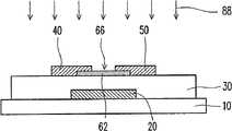
图3A至3C是依照本发明实施例所绘示的一种反交叠型结构的半导体氧化物晶体管的制造方法流程剖面示意图。3A to 3C are schematic cross-sectional views of a manufacturing method of a semiconductor oxide transistor with an inverted overlap structure according to an embodiment of the present invention.
请参照图3A,依照上述的方法形成栅极20、介电层30、第一有源层62以及源极40以及漏极50。源极40与漏极50之间以间隙66相隔开。同样地,可以选择性进行上述的表面处理工艺88,以使第一有源层62的组成配比更稳定。Referring to FIG. 3A , the
接着,请参照图3B,依照上述的方法将间隙66所裸露的第一有源层62移除,形成更深的间隙68。之后,进行另一表面处理工艺90。表面处理工艺90例如是等离子体工艺。等离子体工艺包括氢等离子体工艺、含氢离子等离子体工艺或含氧离子的等离子体工艺。在实施例中,第二有源层64的材料为氧化锌,以氢等离子体工艺或是含氢离子等离子体工艺处理之后,可以提升氧化锌的导电性。Next, referring to FIG. 3B , the first
之后,请参照图3C,依照上述的方法于基板10上形成第二有源层64。第二有源层64覆盖源极40以及漏极50并且填入于间隙68之中,与第一有源层62电性连接。第一有源层62与第二有源层64构成有源层堆叠结构60。源极40以及漏极50之间的有源层堆叠结构60为晶体管的沟道70。Afterwards, referring to FIG. 3C , the second
之后,在基板10上形成保护层80,以覆盖基板10上的顶层。在此例中,所述的顶层包括介电层30、源极40以及漏极50以及有源层堆叠结构60。Afterwards, a
上述方法所形成的半导体氧化物晶体管100d的结构与上述半导体氧化物晶体管100c的结构相同,在此不再赘述。The structure of the
图4A至4C是依照本发明实施例所绘示的一种共平面结构型的半导体氧化物晶体管的制造方法流程剖面示意图。图11为图4A至4C的共平面型结构的半导体氧化物晶体管的制造方法流程图。4A to 4C are cross-sectional schematic diagrams illustrating a manufacturing method of a coplanar semiconductor oxide transistor according to an embodiment of the present invention. FIG. 11 is a flowchart of a method for fabricating the semiconductor oxide transistor with the coplanar structure shown in FIGS. 4A to 4C .
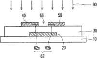
请参照图4A与图11,进行步骤220,在基板10上形成第一有源层62。其后,进行步骤230,在第一有源层62上形成源极40以及漏极50。源极40以及漏极50彼此分隔且具有间隙66。之后,进行步骤235,选择性进行表面处理工艺88,以使第一有源层62的组成配比更稳定。表面处理工艺88例如是等离子体工艺。等离子体工艺包括氢等离子体工艺、含氢离子等离子体工艺或含氧离子的等离子体工艺。Referring to FIG. 4A and FIG. 11 ,
其后,请参照图4B与图11,进行步骤240,在基板10上形成第二有源层64。第二有源层64覆盖源极40以及漏极50,并且填入于间隙66之中,与第一有源层62电性连接。在此将第一有源层62中填入于间隙66之中的部分称为延伸部64a,其位于源极40以及漏极50之间,作为晶体管的沟道70。换言之,第一有源层62与第二有源层64构成有源层堆叠结构60。源极40以及漏极50在有源层堆叠结构60周围并且延伸到有源层堆叠结构60之中,源极40以及漏极50之间的有源层堆叠结构60为晶体管的沟道70。Thereafter, referring to FIG. 4B and FIG. 11 ,
之后,请参照图4C与图11,进行步骤250,在源极40、漏极50、第一有源层62以及基板10上形成介电层30。接着,进行步骤260,在介电层30上形成栅极20。其后,进行步骤270,在基板10上形成保护层80,以覆盖基板10上的介电层30以及栅极20。After that, referring to FIG. 4C and FIG. 11 ,
上述方法所形成的半导体氧化物晶体管100e的栅极20位于介电层30的第二表面30b上,有源层堆叠结构60位于介电层30的第一表面30a上。有源层堆叠结构60包括第一有源层62与第二有源层64。第二有源层64包括延伸部64a,其与第一有源层62的上表面62c接触。源极40以及漏极50在有源层堆叠结构60周围并且延伸到有源层堆叠结构60的第一有源层62与第二有源层64之间,而且源极40以及漏极50之间的有源层堆叠结构60为沟道70。基板10相对于介电层的第一表面30a而覆盖有源层堆叠结构60、源极40、漏极50与介电层30。保护层80相对于介电层30的第二表面30b而覆盖栅极20与介电层30。The
图5A至5C是依照本发明实施例所绘示的另一种共平面结构型的半导体氧化物晶体管的制造方法流程剖面示意图。5A to 5C are cross-sectional schematic diagrams illustrating the process flow of another method for manufacturing a coplanar semiconductor oxide transistor according to an embodiment of the present invention.
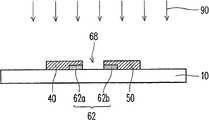
请参照图5A,依照上述方法于基板10上形成第一有源层62以及源极40以及彼此分隔且具有间隙66的漏极50。同样地,其后,可以选择性进行表面处理工艺88,以使第一有源层62的组成配比更稳定。Referring to FIG. 5A , a first
接着,请参照图5B,将间隙66所裸露的第一有源层62移除,形成更深的间隙68。间隙68将第一有源层62分成两部分62a、62b且暴露出介电层30。移除的方法可以采用上述的方法,在此不再赘述。Next, referring to FIG. 5B , the first
之后,请参照图5C,在基板10上形成第二有源层64。第二有源层64覆盖源极40以及漏极50并且填入于间隙68之中,与第一有源层62电性连接。第一有源层62与第二有源层64构成有源层堆叠结构60。第二有源层64中填入于间隙68之中的部分为第二有源层64的延伸部64b,其位于源极40以及漏极50之间,作为晶体管的沟道70。After that, referring to FIG. 5C , a second
之后,在基板10上形成介电层30,接着于介电层30上形成栅极20。其后,在基板10上形成保护层80,以覆盖基板10上的介电层30以及栅极20。After that, a
上述方法所形成的半导体氧化物晶体管100f与半导体氧化物晶体管100e相似,其栅极20位于介电层30的第二表面30b上,有源层堆叠结构60位于介电层30的第一表面30a上。基板10相对于介电层的第一表面30a而覆盖有源层堆叠结构60、源极40、漏极50与介电层30。保护层80相对于介电层30的第二表面30b而覆盖栅极20与介电层30。有源层堆叠结构60包括第一有源层62与第二有源层64。惟,第一有源层62分成两部分62a、62b,且第二有源层64的延伸部64b更向下延伸而与第一有源层62的侧壁62d接触。The
图6A至6C是依照本发明实施例所绘示的另一种共平面结构型的半导体氧化物晶体管的制造方法流程剖面示意图。6A to 6C are cross-sectional schematic diagrams illustrating the process flow of another method for manufacturing a coplanar semiconductor oxide transistor according to an embodiment of the present invention.
请参照图6A,依照上述方法于基板10上形成第一有源层62以及源极40以及漏极50。源极40以及漏极50彼此分隔且具有间隙66。同样地,其后,可以选择性进行表面处理工艺88,以使第一有源层62的组成配比更稳定。Referring to FIG. 6A , the first
接着,请参照图6B,将间隙66所裸露的第一有源层62移除,形成更深的间隙68。之后,进行表面处理工艺90。表面处理工艺如上所述,在此不再赘述。Next, referring to FIG. 6B , the first
之后,请参照图6C,在基板10上形成第二有源层64。第二有源层64覆盖源极40以及漏极50并且填入于间隙68之中,与第一有源层62电性连接。第一有源层62与第二有源层64构成有源层堆叠结构60,第二有源层64中填入于间隙68之中的部分为延伸部64b,其位于源极40以及漏极50之间,作为晶体管的沟道70。After that, referring to FIG. 6C , a second
之后,在基板10上形成介电层30,接着于介电层30上形成栅极20。其后,在基板10上形成保护层80,以覆盖基板10上的介电层30以及栅极20。After that, a
上述方法所形成的半导体氧化物晶体管100g的结构与上述半导体氧化物晶体管100f的结构相同,在此不再赘述。The structure of the
上述基板10例如是硬式基板或是软式基板。玻璃基板、硅晶片基板、金属基板。软性基板的材料例如是塑胶基板或金属箔(Metal Foil)。塑胶基板的材料例如是聚乙烯对苯二甲酸酯(polyethylene terephthalate,PET)、聚二甲酸乙二醇酯(polyethylene naphthalate,PEN)、聚酯(polyester,PES)、聚甲基丙烯酸甲酯(polymethylmethacrylate,PMMA)、聚碳酸酯(polycarbonate,PC)或聚酰亚胺(polyimide,PI)。The
栅极20的材料例如是Au、Ag、Cu、Ni、Cr、Ti、Al、Pt、Pd金属或其合金,或是前述材料所形成的堆叠结构例如是钛/铝/钛所组成的堆叠结构或是钼/铝所组成的堆叠结构。栅极20的形成方法例如是以物理气相沉积(Physical vapor deposition,PVD)、化学气相沉积(Chemical vapor deposition,CVD)、溶液态工艺沉积(Solution-processed deposition)、电镀沉积(Electroplating deposition)或无电镀沉积(Electroless plating deposition),或其他类似的方法所形成的未图案化的薄膜,再经由图案化工艺例如是光刻与蚀刻工艺形成。栅极20的形成方法也可以例如以喷墨印刷沉积方式,在低温下直接形成已图案化的薄膜。The material of the
上述介电层30可以是单层或是多层结构。介电层30可为无机材料、有机材料或是无机材料与有机材料的混合材料(hybrid)。无机材料例如是氧化硅、氮化硅或是氮氧化硅。有机材料例如聚乙烯吡咯烷酮(Polyvinylprrolidone,PVP)、聚亚酰胺(PI)、聚乙烯酚(Polyvinyl phenol)、聚苯乙烯(PS)、压克力或环氧树脂。介电层30的形成方法可以采用化学气相沉积法、旋镀或是涂布等方法。The above-mentioned
上述源极40以及漏极50的形成方法例如是先形成一层导电材料层,然后,再将其图案化。导电材料层的材料例如是金属或是透明导电氧化物。金属例如是金、银、铝、铜、铬、镍、钛、铂、钯或前述材料的合金,或是前述材料所形成的堆叠结构例如是钛/铝/钛所组成的堆叠结构或是钼/铝所组成的堆叠结构。导电材料层的形成方法包括进行物理气相沉积工艺,物理气相沉积工艺例如是溅镀工艺或是蒸镀工艺。导电材料层的厚度例如是100-300nm。图案化的方法例如是光刻与蚀刻法。在另一实施例中,源极与漏极的形成方法也可以直接形成图案化的导电层,例如是以喷墨工艺来施行。The method for forming the
第一有源层62的材料与第二有源层64的材料可以是氧化物半导体。此处所述的氧化物半导体层只是一个通称,其电阻率可以在10-2至1018Ω-cm之间,也就是,可以是绝缘体、半导体或是导体,并不以半导体为限。氧化物半导体层的组成由二元或二元以上的过渡金属与氧,例如是二元到五元的过渡金属与氧所构成。氧化物半导体层的材料例如是IZO(In-Zn-O)、GZO(Ga-Zn-O)、ZnO、GaO、IGZO(In-Ga-Zn-O)或ATZO(Al-Sn-Zn-O)等材料。第一有源层62与第二有源层64的氧化物半导体层的组成可以相同或是相异。在一实施例中,第一有源层62的氧化物半导体层与第二有源层64的氧化物半导体层的组成相同且组份比相同。在另一实施例中,第一有源层62的氧化物半导体层与第二有源层64的氧化物半导体层的组成相同但组份比不同,例如是第一有源层62与第二有源层64同样是由IGZO所构成,但是第一有源层62的组份比为In∶Ga∶Zn∶O=1∶1∶1∶4,第二有源层64的组份比为In∶Ga∶Zn∶O=2∶1∶1∶7。形成组成相同但组份比不同氧化物半导体层的方法可以通过沉积工艺条件的调变,例如是含氧量来达成。第一有源层62与第二有源层64的形成方法例如是可以采用物理气相沉积法(PVD),如溅镀法、蒸镀法或离子束镀膜法或是化学气相沉积法(CVD)。第一有源层62与第二有源层64的厚度可以依照实际的需要而定,可以相同或相异。The material of the first
保护层80可以避免元件暴露于大气之中遭受水气、氧气的侵袭或在后续的过程中遭受蚀刻的破坏。保护层80的材料可以是单层或是多层结构。保护层80可为无机材料、有机材料或是无机材料与有机材料的混合材料(hybrid)。无机材料例如是氧化硅、氮化硅或是氮氧化硅。有机材料例如聚乙烯吡咯烷酮(Polyvinylprrolidone,PVP)、聚亚酰胺(PI)、聚乙烯酚(Polyvinylphenol)、聚苯乙烯(PS)、压克力或环氧树脂。保护层80的形成方法可以采用化学气相沉积法、旋镀或是涂布等方法。The
电极层104与电极层110例如是透明导电氧化物薄膜、透明金属薄膜或是透明纳米碳管(CNT)。透明导电氧化物例如是铟锡氧化物(Indium TinOxide,ITO)、铟锌氧化物(Indium Zinc Oxide,IZO)、掺铝氧化锌(Aluminumdoped zinc oxide,AZO)或是其他透明导电材料。透明金属薄膜例如是金、银、铝、铜、铬、镍、钛、铂、钯或前述材料的合金等。电极层104与电极层110的形成方法包括溅镀工艺或旋镀工艺(spin-coating)。电极层104与电极层110的厚度例如是约为100至500纳米(nm)。The
有机发光层108的材料例如适于发出红、蓝、绿或其他单色光的有机材料。The material of the organic
在以上的实施中仅以图1D-1E来说明晶体管应用于有机发光二极管显示器,然上述方法所形成晶体管均可以应用于有机发光二极管等。In the above implementation, only FIGS. 1D-1E are used to illustrate that the transistor is applied to the OLED display, but the transistor formed by the above method can be applied to the OLED or the like.
实验例1Experimental example 1
制作图1B的半导体氧化物晶体管。其中栅极以及源极与漏极均是以溅镀方法形成的100nm的MoW。介电层是以化学气相沉积方法形成的150nm的氮化硅。源极与漏极下方的有源层是以溅镀方法形成的50nm的IGZO(In∶Ga∶Zn∶O=1∶1∶1∶4)。源极与漏极上方的有源层是以溅镀方法形成的100nm的IGZO(In∶Ga∶Zn∶O=2∶1∶1∶7)。Fabricate the semiconductor oxide transistor of Figure 1B. The gate, source and drain are all 100nm MoW formed by sputtering. The dielectric layer is 150nm silicon nitride formed by chemical vapor deposition. The active layer below the source and drain is 50nm IGZO (In:Ga:Zn:O=1:1:1:4) formed by sputtering. The active layer above the source and drain is 100nm IGZO (In:Ga:Zn:O=2:1:1:7) formed by sputtering.
之后,在不同的条件下进行电性测试。在较大的饱和电流Id以及电压Vg(Id=80μA;Vg=20V)下进行测试的结果如图7所示。在一般条件下(Id=6μA;Vg=10V)进行测试的结果则如图8所示。图9则是实验例1所形成的半导体氧化物晶体管在施加应力(stress)前后电性的测试结果。Afterwards, electrical tests were performed under different conditions. The results of testing under a relatively large saturation current Id and voltage Vg (Id=80 μA; Vg=20V) are shown in FIG. 7 . The test results under normal conditions (Id=6 μA; Vg=10V) are shown in FIG. 8 . FIG. 9 shows the test results of the electrical properties of the semiconductor oxide transistor formed in Experimental Example 1 before and after applying stress.
比较例1Comparative example 1
以相同实验例1的方法制造半导体氧化物晶体管,但,源极与漏极上方不形成有源层。A semiconductor oxide transistor was manufactured in the same manner as in Experimental Example 1, but no active layer was formed over the source and drain.
比较例2Comparative example 2
以相同实验例1的方法制造半导体氧化物晶体管,但,源极与漏极下方的有源层改变为100nm的IGZO(In∶Ga∶Zn∶O=1∶1∶1∶4),且源极与漏极上方不形成有源层。A semiconductor oxide transistor was fabricated by the same method as
比较例3Comparative example 3
以相同实验例1的方法制造半导体氧化物晶体管,但,源极与漏极下方的有源层改变为200nm的IGZO(In∶Ga∶Zn∶O=1∶1∶1∶4),且源极与漏极上方不形成有源层。A semiconductor oxide transistor was fabricated by the same method as in Experimental Example 1, but the active layer under the source and drain was changed to 200nm IGZO (In:Ga:Zn:O=1:1:1:4), and the source No active layer is formed above the electrode and the drain.
由图7、8的结果显示半导体氧化物晶体管应用于OLED时,元件的寿命大于3年。而由图9的结果显示:时间经过2×10⁵秒之后,起始电压仅飘移0.005V,表示元件具有良好的稳定性。The results shown in Figures 7 and 8 show that when semiconductor oxide transistors are applied to OLEDs, the lifetime of the elements is greater than 3 years. The results shown in Fig. 9 show that after 2×10⁵ seconds, the initial voltage only shifted by 0.005V, indicating that the device has good stability.
由实验例1与比较例1-3的结果显示:采用两层有源层的半导体氧化物晶体管比采用单层有源层的半导体氧化物晶体管具有优选的电性。再者,实验例1与比较例3的结果显示:虽然实验例1的两层有源层的总厚度小于比较例3单层的有源晶体管厚度,但是,实验1的半导体氧化物晶体管的电性仍优于比较例3,此结果表示电性的提升并非单纯因为厚度增加所造成,本发明采有源层堆叠对元件的电性有正面提升的作用。The results of Experimental Example 1 and Comparative Examples 1-3 show that the semiconductor oxide transistor using two active layers has better electrical properties than the semiconductor oxide transistor using a single active layer. Furthermore, the results of Experimental Example 1 and Comparative Example 3 show that although the total thickness of the two active layers in Experimental Example 1 is smaller than the thickness of the single-layer active transistor in Comparative Example 3, the electrical conductivity of the semiconductor oxide transistor in
综合以上所述,本发明实施例的半导体氧化物晶体管,采用有源层堆叠结构,不需使用沟道保护层或酸液处理,即可提高元件的稳定性。Based on the above, the semiconductor oxide transistor of the embodiment of the present invention adopts the stacked active layer structure, which can improve the stability of the device without using a channel protection layer or acid treatment.
虽然本发明已以实施例披露如上,然其并非用以限定本发明,任何所属技术领域中普通技术人员,在不脱离本发明的精神和范围内,当可作些许的更动与润饰,故本发明的保护范围当视权利要求所界定为准。Although the present invention has been disclosed above with embodiments, it is not intended to limit the present invention. Any person skilled in the art may make some modifications and modifications without departing from the spirit and scope of the present invention. The scope of protection of the present invention should be defined by the claims.
Claims (28)
Translated fromChinesePriority Applications (1)
| Application Number | Priority Date | Filing Date | Title |
|---|---|---|---|
| CN2010102092387ACN102290440A (en) | 2010-06-21 | 2010-06-21 | Transistor and method of manufacturing the same |
Applications Claiming Priority (1)
| Application Number | Priority Date | Filing Date | Title |
|---|---|---|---|
| CN2010102092387ACN102290440A (en) | 2010-06-21 | 2010-06-21 | Transistor and method of manufacturing the same |
Publications (1)
| Publication Number | Publication Date |
|---|---|
| CN102290440Atrue CN102290440A (en) | 2011-12-21 |
Family
ID=45336693
Family Applications (1)
| Application Number | Title | Priority Date | Filing Date |
|---|---|---|---|
| CN2010102092387APendingCN102290440A (en) | 2010-06-21 | 2010-06-21 | Transistor and method of manufacturing the same |
Country Status (1)
| Country | Link |
|---|---|
| CN (1) | CN102290440A (en) |
Cited By (6)
| Publication number | Priority date | Publication date | Assignee | Title |
|---|---|---|---|---|
| CN102637742A (en)* | 2012-04-26 | 2012-08-15 | 北京大学 | Oxide semiconductor thin-film transistor and preparation method thereof |
| CN102709316A (en)* | 2012-05-30 | 2012-10-03 | 北京大学 | Three-dimensional (3D) oxide semiconductor thin film transistor and preparation method thereof |
| CN103137641A (en)* | 2013-01-25 | 2013-06-05 | 北京京东方光电科技有限公司 | Array substrate and manufacturing method thereof and X ray flat plate detector |
| CN104659210A (en)* | 2013-11-21 | 2015-05-27 | 元太科技工业股份有限公司 | Transistor structure and manufacturing method thereof |
| WO2015100808A1 (en)* | 2013-12-31 | 2015-07-09 | 深圳市华星光电技术有限公司 | Light-emitting apparatus provided with oxide thin-film transistor, and manufacturing method therefor |
| WO2023241006A1 (en)* | 2022-06-14 | 2023-12-21 | 东南大学 | Phase inverter based on igzo thin-film transistor, and preparation method therefor |
Citations (8)
| Publication number | Priority date | Publication date | Assignee | Title |
|---|---|---|---|---|
| JPH05218418A (en)* | 1992-02-03 | 1993-08-27 | Nec Corp | Thin film transistor |
| US5648662A (en)* | 1991-06-19 | 1997-07-15 | Semiconductor Energy Laboratory Co., Ltd. | Electro-optical device with amorphous and crystalline shift registers |
| JP2002110992A (en)* | 2000-09-28 | 2002-04-12 | Matsushita Electric Ind Co Ltd | Thin film transistor, method of manufacturing the same, and liquid crystal display device using the same |
| US20060079034A1 (en)* | 2004-10-12 | 2006-04-13 | Randy Hoffman | Method to form a passivation layer |
| US20080296568A1 (en)* | 2007-05-29 | 2008-12-04 | Samsung Electronics Co., Ltd | Thin film transistors and methods of manufacturing the same |
| US20090050884A1 (en)* | 2007-08-02 | 2009-02-26 | Yan Ye | Thin film transistors using thin film semiconductor materials |
| WO2009028453A1 (en)* | 2007-08-31 | 2009-03-05 | Konica Minolta Holdings, Inc. | Thin film transistor |
| US20100065842A1 (en)* | 2008-09-12 | 2010-03-18 | Semiconductor Energy Laboratory Co., Ltd. | Semiconductor device and manufacturing method thereof |
- 2010
- 2010-06-21CNCN2010102092387Apatent/CN102290440A/enactivePending
Patent Citations (8)
| Publication number | Priority date | Publication date | Assignee | Title |
|---|---|---|---|---|
| US5648662A (en)* | 1991-06-19 | 1997-07-15 | Semiconductor Energy Laboratory Co., Ltd. | Electro-optical device with amorphous and crystalline shift registers |
| JPH05218418A (en)* | 1992-02-03 | 1993-08-27 | Nec Corp | Thin film transistor |
| JP2002110992A (en)* | 2000-09-28 | 2002-04-12 | Matsushita Electric Ind Co Ltd | Thin film transistor, method of manufacturing the same, and liquid crystal display device using the same |
| US20060079034A1 (en)* | 2004-10-12 | 2006-04-13 | Randy Hoffman | Method to form a passivation layer |
| US20080296568A1 (en)* | 2007-05-29 | 2008-12-04 | Samsung Electronics Co., Ltd | Thin film transistors and methods of manufacturing the same |
| US20090050884A1 (en)* | 2007-08-02 | 2009-02-26 | Yan Ye | Thin film transistors using thin film semiconductor materials |
| WO2009028453A1 (en)* | 2007-08-31 | 2009-03-05 | Konica Minolta Holdings, Inc. | Thin film transistor |
| US20100065842A1 (en)* | 2008-09-12 | 2010-03-18 | Semiconductor Energy Laboratory Co., Ltd. | Semiconductor device and manufacturing method thereof |
Cited By (8)
| Publication number | Priority date | Publication date | Assignee | Title |
|---|---|---|---|---|
| CN102637742A (en)* | 2012-04-26 | 2012-08-15 | 北京大学 | Oxide semiconductor thin-film transistor and preparation method thereof |
| CN102709316A (en)* | 2012-05-30 | 2012-10-03 | 北京大学 | Three-dimensional (3D) oxide semiconductor thin film transistor and preparation method thereof |
| CN102709316B (en)* | 2012-05-30 | 2015-02-18 | 京东方科技集团股份有限公司 | Three-dimensional (3D) oxide semiconductor thin film transistor and preparation method thereof |
| CN103137641A (en)* | 2013-01-25 | 2013-06-05 | 北京京东方光电科技有限公司 | Array substrate and manufacturing method thereof and X ray flat plate detector |
| CN103137641B (en)* | 2013-01-25 | 2015-10-21 | 北京京东方光电科技有限公司 | A kind of array base palte and preparation method thereof, X-ray flat panel detector |
| CN104659210A (en)* | 2013-11-21 | 2015-05-27 | 元太科技工业股份有限公司 | Transistor structure and manufacturing method thereof |
| WO2015100808A1 (en)* | 2013-12-31 | 2015-07-09 | 深圳市华星光电技术有限公司 | Light-emitting apparatus provided with oxide thin-film transistor, and manufacturing method therefor |
| WO2023241006A1 (en)* | 2022-06-14 | 2023-12-21 | 东南大学 | Phase inverter based on igzo thin-film transistor, and preparation method therefor |
Similar Documents
| Publication | Publication Date | Title |
|---|---|---|
| TWI443829B (en) | Transistor and manufacturing method thereof | |
| US12389678B2 (en) | Method for fabricating array substrate | |
| US9391097B2 (en) | Thin film transistor, array substrate and method of manufacturing the same and display device | |
| CN104637438B (en) | Flexible display and its manufacturing method | |
| CN102403365B (en) | Thin film transistor and method of manufacturing the same | |
| US20140145179A1 (en) | Tft, method of manufacturing the tft, and method of manufacturing organic light emitting display device including the tft | |
| TW201413975A (en) | Thin film transistor array substrate and manufacturing method thereof | |
| WO2018006441A1 (en) | Thin film transistor, array substrate and manufacturing method therefor | |
| US7981708B1 (en) | Method of fabricating pixel structure and method of fabricating organic light emitting device | |
| KR101922937B1 (en) | Thin film transistor array substrate and method for fabricating the same | |
| US9214476B1 (en) | Pixel structure | |
| CN104517972B (en) | Display device and its manufacturing method | |
| CN102290440A (en) | Transistor and method of manufacturing the same | |
| WO2016123974A1 (en) | Thin-film transistor, pixel structure, manufacturing methods therefor, array substrate and display device | |
| TW201123441A (en) | Organic light-emitting display and method of manufacturing the same | |
| CN105097710A (en) | Thin film transistor array substrate and manufacturing method thereof | |
| CN107731882A (en) | A kind of organic thin film transistor array substrate and preparation method thereof, display device | |
| CN105118836A (en) | Array substrate with conductive flat layers and manufacturing method thereof | |
| CN107039500A (en) | Thin film transistor of display panel | |
| CN109638050B (en) | Display panel and manufacturing method thereof | |
| WO2016123979A1 (en) | Thin-film transistor and manufacturing method therefor, array substrate and display device | |
| KR102044971B1 (en) | Thin film transistor substrate and method of manufacturing the same | |
| CN111162112A (en) | Double-sided OLED display structure and manufacturing method | |
| CN105304653B (en) | Dot structure, array substrate, liquid crystal display panel and dot structure manufacturing method | |
| CN118039702A (en) | Top gate Schottky oxide thin film transistor and preparation method thereof |
Legal Events
| Date | Code | Title | Description |
|---|---|---|---|
| C06 | Publication | ||
| PB01 | Publication | ||
| C10 | Entry into substantive examination | ||
| SE01 | Entry into force of request for substantive examination | ||
| C12 | Rejection of a patent application after its publication | ||
| RJ01 | Rejection of invention patent application after publication | Application publication date:20111221 |