CN102282661A - Method for mounting semiconductor chip, semiconductor device obtained by the method, method for connecting semiconductor chip, three-dimensional structure with wiring on its surface, and method for manufacturing the same - Google Patents
Method for mounting semiconductor chip, semiconductor device obtained by the method, method for connecting semiconductor chip, three-dimensional structure with wiring on its surface, and method for manufacturing the sameDownload PDFInfo
- Publication number
- CN102282661A CN102282661ACN2010800045943ACN201080004594ACN102282661ACN 102282661 ACN102282661 ACN 102282661ACN 2010800045943 ACN2010800045943 ACN 2010800045943ACN 201080004594 ACN201080004594 ACN 201080004594ACN 102282661 ACN102282661 ACN 102282661A
- Authority
- CN
- China
- Prior art keywords
- wiring
- semiconductor chip
- resin
- dimensional structure
- film
- Prior art date
- Legal status (The legal status is an assumption and is not a legal conclusion. Google has not performed a legal analysis and makes no representation as to the accuracy of the status listed.)
- Pending
Links
Images


Classifications
- H—ELECTRICITY
- H05—ELECTRIC TECHNIQUES NOT OTHERWISE PROVIDED FOR
- H05K—PRINTED CIRCUITS; CASINGS OR CONSTRUCTIONAL DETAILS OF ELECTRIC APPARATUS; MANUFACTURE OF ASSEMBLAGES OF ELECTRICAL COMPONENTS
- H05K1/00—Printed circuits
- H05K1/02—Details
- H05K1/11—Printed elements for providing electric connections to or between printed circuits
- G—PHYSICS
- G11—INFORMATION STORAGE
- G11B—INFORMATION STORAGE BASED ON RELATIVE MOVEMENT BETWEEN RECORD CARRIER AND TRANSDUCER
- G11B5/00—Recording by magnetisation or demagnetisation of a record carrier; Reproducing by magnetic means; Record carriers therefor
- G11B5/48—Disposition or mounting of heads or head supports relative to record carriers ; arrangements of heads, e.g. for scanning the record carrier to increase the relative speed
- G11B5/4806—Disposition or mounting of heads or head supports relative to record carriers ; arrangements of heads, e.g. for scanning the record carrier to increase the relative speed specially adapted for disk drive assemblies, e.g. assembly prior to operation, hard or flexible disk drives
- G11B5/486—Disposition or mounting of heads or head supports relative to record carriers ; arrangements of heads, e.g. for scanning the record carrier to increase the relative speed specially adapted for disk drive assemblies, e.g. assembly prior to operation, hard or flexible disk drives with provision for mounting or arranging electrical conducting means or circuits on or along the arm assembly
- H—ELECTRICITY
- H01—ELECTRIC ELEMENTS
- H01L—SEMICONDUCTOR DEVICES NOT COVERED BY CLASS H10
- H01L23/00—Details of semiconductor or other solid state devices
- H01L23/52—Arrangements for conducting electric current within the device in operation from one component to another, i.e. interconnections, e.g. wires, lead frames
- H—ELECTRICITY
- H01—ELECTRIC ELEMENTS
- H01L—SEMICONDUCTOR DEVICES NOT COVERED BY CLASS H10
- H01L23/00—Details of semiconductor or other solid state devices
- H01L23/48—Arrangements for conducting electric current to or from the solid state body in operation, e.g. leads, terminal arrangements ; Selection of materials therefor
- H—ELECTRICITY
- H01—ELECTRIC ELEMENTS
- H01L—SEMICONDUCTOR DEVICES NOT COVERED BY CLASS H10
- H01L24/00—Arrangements for connecting or disconnecting semiconductor or solid-state bodies; Methods or apparatus related thereto
- H01L24/01—Means for bonding being attached to, or being formed on, the surface to be connected, e.g. chip-to-package, die-attach, "first-level" interconnects; Manufacturing methods related thereto
- H01L24/02—Bonding areas ; Manufacturing methods related thereto
- H01L24/03—Manufacturing methods
- H—ELECTRICITY
- H01—ELECTRIC ELEMENTS
- H01L—SEMICONDUCTOR DEVICES NOT COVERED BY CLASS H10
- H01L24/00—Arrangements for connecting or disconnecting semiconductor or solid-state bodies; Methods or apparatus related thereto
- H01L24/01—Means for bonding being attached to, or being formed on, the surface to be connected, e.g. chip-to-package, die-attach, "first-level" interconnects; Manufacturing methods related thereto
- H01L24/02—Bonding areas ; Manufacturing methods related thereto
- H01L24/04—Structure, shape, material or disposition of the bonding areas prior to the connecting process
- H01L24/05—Structure, shape, material or disposition of the bonding areas prior to the connecting process of an individual bonding area
- H—ELECTRICITY
- H01—ELECTRIC ELEMENTS
- H01L—SEMICONDUCTOR DEVICES NOT COVERED BY CLASS H10
- H01L24/00—Arrangements for connecting or disconnecting semiconductor or solid-state bodies; Methods or apparatus related thereto
- H01L24/01—Means for bonding being attached to, or being formed on, the surface to be connected, e.g. chip-to-package, die-attach, "first-level" interconnects; Manufacturing methods related thereto
- H01L24/18—High density interconnect [HDI] connectors; Manufacturing methods related thereto
- H01L24/23—Structure, shape, material or disposition of the high density interconnect connectors after the connecting process
- H01L24/24—Structure, shape, material or disposition of the high density interconnect connectors after the connecting process of an individual high density interconnect connector
- H—ELECTRICITY
- H01—ELECTRIC ELEMENTS
- H01L—SEMICONDUCTOR DEVICES NOT COVERED BY CLASS H10
- H01L24/00—Arrangements for connecting or disconnecting semiconductor or solid-state bodies; Methods or apparatus related thereto
- H01L24/01—Means for bonding being attached to, or being formed on, the surface to be connected, e.g. chip-to-package, die-attach, "first-level" interconnects; Manufacturing methods related thereto
- H01L24/18—High density interconnect [HDI] connectors; Manufacturing methods related thereto
- H01L24/23—Structure, shape, material or disposition of the high density interconnect connectors after the connecting process
- H01L24/25—Structure, shape, material or disposition of the high density interconnect connectors after the connecting process of a plurality of high density interconnect connectors
- H—ELECTRICITY
- H01—ELECTRIC ELEMENTS
- H01L—SEMICONDUCTOR DEVICES NOT COVERED BY CLASS H10
- H01L24/00—Arrangements for connecting or disconnecting semiconductor or solid-state bodies; Methods or apparatus related thereto
- H01L24/80—Methods for connecting semiconductor or other solid state bodies using means for bonding being attached to, or being formed on, the surface to be connected
- H01L24/82—Methods for connecting semiconductor or other solid state bodies using means for bonding being attached to, or being formed on, the surface to be connected by forming build-up interconnects at chip-level, e.g. for high density interconnects [HDI]
- H—ELECTRICITY
- H01—ELECTRIC ELEMENTS
- H01L—SEMICONDUCTOR DEVICES NOT COVERED BY CLASS H10
- H01L25/00—Assemblies consisting of a plurality of semiconductor or other solid state devices
- H01L25/03—Assemblies consisting of a plurality of semiconductor or other solid state devices all the devices being of a type provided for in a single subclass of subclasses H10B, H10D, H10F, H10H, H10K or H10N, e.g. assemblies of rectifier diodes
- H01L25/04—Assemblies consisting of a plurality of semiconductor or other solid state devices all the devices being of a type provided for in a single subclass of subclasses H10B, H10D, H10F, H10H, H10K or H10N, e.g. assemblies of rectifier diodes the devices not having separate containers
- H01L25/065—Assemblies consisting of a plurality of semiconductor or other solid state devices all the devices being of a type provided for in a single subclass of subclasses H10B, H10D, H10F, H10H, H10K or H10N, e.g. assemblies of rectifier diodes the devices not having separate containers the devices being of a type provided for in group H10D89/00
- H01L25/0655—Assemblies consisting of a plurality of semiconductor or other solid state devices all the devices being of a type provided for in a single subclass of subclasses H10B, H10D, H10F, H10H, H10K or H10N, e.g. assemblies of rectifier diodes the devices not having separate containers the devices being of a type provided for in group H10D89/00 the devices being arranged next to each other
- H—ELECTRICITY
- H01—ELECTRIC ELEMENTS
- H01L—SEMICONDUCTOR DEVICES NOT COVERED BY CLASS H10
- H01L25/00—Assemblies consisting of a plurality of semiconductor or other solid state devices
- H01L25/03—Assemblies consisting of a plurality of semiconductor or other solid state devices all the devices being of a type provided for in a single subclass of subclasses H10B, H10D, H10F, H10H, H10K or H10N, e.g. assemblies of rectifier diodes
- H01L25/04—Assemblies consisting of a plurality of semiconductor or other solid state devices all the devices being of a type provided for in a single subclass of subclasses H10B, H10D, H10F, H10H, H10K or H10N, e.g. assemblies of rectifier diodes the devices not having separate containers
- H01L25/065—Assemblies consisting of a plurality of semiconductor or other solid state devices all the devices being of a type provided for in a single subclass of subclasses H10B, H10D, H10F, H10H, H10K or H10N, e.g. assemblies of rectifier diodes the devices not having separate containers the devices being of a type provided for in group H10D89/00
- H01L25/0657—Stacked arrangements of devices
- H—ELECTRICITY
- H01—ELECTRIC ELEMENTS
- H01L—SEMICONDUCTOR DEVICES NOT COVERED BY CLASS H10
- H01L25/00—Assemblies consisting of a plurality of semiconductor or other solid state devices
- H01L25/50—Multistep manufacturing processes of assemblies consisting of devices, the devices being individual devices of subclass H10D or integrated devices of class H10
- H—ELECTRICITY
- H05—ELECTRIC TECHNIQUES NOT OTHERWISE PROVIDED FOR
- H05K—PRINTED CIRCUITS; CASINGS OR CONSTRUCTIONAL DETAILS OF ELECTRIC APPARATUS; MANUFACTURE OF ASSEMBLAGES OF ELECTRICAL COMPONENTS
- H05K1/00—Printed circuits
- H05K1/02—Details
- H05K1/11—Printed elements for providing electric connections to or between printed circuits
- H05K1/111—Pads for surface mounting, e.g. lay-out
- H—ELECTRICITY
- H05—ELECTRIC TECHNIQUES NOT OTHERWISE PROVIDED FOR
- H05K—PRINTED CIRCUITS; CASINGS OR CONSTRUCTIONAL DETAILS OF ELECTRIC APPARATUS; MANUFACTURE OF ASSEMBLAGES OF ELECTRICAL COMPONENTS
- H05K1/00—Printed circuits
- H05K1/02—Details
- H05K1/11—Printed elements for providing electric connections to or between printed circuits
- H05K1/117—Pads along the edge of rigid circuit boards, e.g. for pluggable connectors
- H—ELECTRICITY
- H05—ELECTRIC TECHNIQUES NOT OTHERWISE PROVIDED FOR
- H05K—PRINTED CIRCUITS; CASINGS OR CONSTRUCTIONAL DETAILS OF ELECTRIC APPARATUS; MANUFACTURE OF ASSEMBLAGES OF ELECTRICAL COMPONENTS
- H05K1/00—Printed circuits
- H05K1/18—Printed circuits structurally associated with non-printed electric components
- H05K1/181—Printed circuits structurally associated with non-printed electric components associated with surface mounted components
- H—ELECTRICITY
- H05—ELECTRIC TECHNIQUES NOT OTHERWISE PROVIDED FOR
- H05K—PRINTED CIRCUITS; CASINGS OR CONSTRUCTIONAL DETAILS OF ELECTRIC APPARATUS; MANUFACTURE OF ASSEMBLAGES OF ELECTRICAL COMPONENTS
- H05K3/00—Apparatus or processes for manufacturing printed circuits
- H05K3/10—Apparatus or processes for manufacturing printed circuits in which conductive material is applied to the insulating support in such a manner as to form the desired conductive pattern
- H05K3/18—Apparatus or processes for manufacturing printed circuits in which conductive material is applied to the insulating support in such a manner as to form the desired conductive pattern using precipitation techniques to apply the conductive material
- H05K3/181—Apparatus or processes for manufacturing printed circuits in which conductive material is applied to the insulating support in such a manner as to form the desired conductive pattern using precipitation techniques to apply the conductive material by electroless plating
- H05K3/182—Apparatus or processes for manufacturing printed circuits in which conductive material is applied to the insulating support in such a manner as to form the desired conductive pattern using precipitation techniques to apply the conductive material by electroless plating characterised by the patterning method
- H05K3/184—Apparatus or processes for manufacturing printed circuits in which conductive material is applied to the insulating support in such a manner as to form the desired conductive pattern using precipitation techniques to apply the conductive material by electroless plating characterised by the patterning method using masks
- H—ELECTRICITY
- H01—ELECTRIC ELEMENTS
- H01L—SEMICONDUCTOR DEVICES NOT COVERED BY CLASS H10
- H01L21/00—Processes or apparatus adapted for the manufacture or treatment of semiconductor or solid state devices or of parts thereof
- H01L21/02—Manufacture or treatment of semiconductor devices or of parts thereof
- H01L21/04—Manufacture or treatment of semiconductor devices or of parts thereof the devices having potential barriers, e.g. a PN junction, depletion layer or carrier concentration layer
- H01L21/50—Assembly of semiconductor devices using processes or apparatus not provided for in a single one of the groups H01L21/18 - H01L21/326 or H10D48/04 - H10D48/07 e.g. sealing of a cap to a base of a container
- H01L21/56—Encapsulations, e.g. encapsulation layers, coatings
- H01L21/565—Moulds
- H—ELECTRICITY
- H01—ELECTRIC ELEMENTS
- H01L—SEMICONDUCTOR DEVICES NOT COVERED BY CLASS H10
- H01L22/00—Testing or measuring during manufacture or treatment; Reliability measurements, i.e. testing of parts without further processing to modify the parts as such; Structural arrangements therefor
- H01L22/10—Measuring as part of the manufacturing process
- H01L22/12—Measuring as part of the manufacturing process for structural parameters, e.g. thickness, line width, refractive index, temperature, warp, bond strength, defects, optical inspection, electrical measurement of structural dimensions, metallurgic measurement of diffusions
- H—ELECTRICITY
- H01—ELECTRIC ELEMENTS
- H01L—SEMICONDUCTOR DEVICES NOT COVERED BY CLASS H10
- H01L2224/00—Indexing scheme for arrangements for connecting or disconnecting semiconductor or solid-state bodies and methods related thereto as covered by H01L24/00
- H01L2224/01—Means for bonding being attached to, or being formed on, the surface to be connected, e.g. chip-to-package, die-attach, "first-level" interconnects; Manufacturing methods related thereto
- H01L2224/02—Bonding areas; Manufacturing methods related thereto
- H01L2224/04—Structure, shape, material or disposition of the bonding areas prior to the connecting process
- H01L2224/04042—Bonding areas specifically adapted for wire connectors, e.g. wirebond pads
- H—ELECTRICITY
- H01—ELECTRIC ELEMENTS
- H01L—SEMICONDUCTOR DEVICES NOT COVERED BY CLASS H10
- H01L2224/00—Indexing scheme for arrangements for connecting or disconnecting semiconductor or solid-state bodies and methods related thereto as covered by H01L24/00
- H01L2224/01—Means for bonding being attached to, or being formed on, the surface to be connected, e.g. chip-to-package, die-attach, "first-level" interconnects; Manufacturing methods related thereto
- H01L2224/02—Bonding areas; Manufacturing methods related thereto
- H01L2224/04—Structure, shape, material or disposition of the bonding areas prior to the connecting process
- H01L2224/05—Structure, shape, material or disposition of the bonding areas prior to the connecting process of an individual bonding area
- H01L2224/0554—External layer
- H01L2224/0555—Shape
- H01L2224/05552—Shape in top view
- H01L2224/05554—Shape in top view being square
- H—ELECTRICITY
- H01—ELECTRIC ELEMENTS
- H01L—SEMICONDUCTOR DEVICES NOT COVERED BY CLASS H10
- H01L2224/00—Indexing scheme for arrangements for connecting or disconnecting semiconductor or solid-state bodies and methods related thereto as covered by H01L24/00
- H01L2224/01—Means for bonding being attached to, or being formed on, the surface to be connected, e.g. chip-to-package, die-attach, "first-level" interconnects; Manufacturing methods related thereto
- H01L2224/10—Bump connectors; Manufacturing methods related thereto
- H01L2224/15—Structure, shape, material or disposition of the bump connectors after the connecting process
- H01L2224/16—Structure, shape, material or disposition of the bump connectors after the connecting process of an individual bump connector
- H01L2224/161—Disposition
- H01L2224/16151—Disposition the bump connector connecting between a semiconductor or solid-state body and an item not being a semiconductor or solid-state body, e.g. chip-to-substrate, chip-to-passive
- H01L2224/16221—Disposition the bump connector connecting between a semiconductor or solid-state body and an item not being a semiconductor or solid-state body, e.g. chip-to-substrate, chip-to-passive the body and the item being stacked
- H01L2224/16225—Disposition the bump connector connecting between a semiconductor or solid-state body and an item not being a semiconductor or solid-state body, e.g. chip-to-substrate, chip-to-passive the body and the item being stacked the item being non-metallic, e.g. insulating substrate with or without metallisation
- H01L2224/16227—Disposition the bump connector connecting between a semiconductor or solid-state body and an item not being a semiconductor or solid-state body, e.g. chip-to-substrate, chip-to-passive the body and the item being stacked the item being non-metallic, e.g. insulating substrate with or without metallisation the bump connector connecting to a bond pad of the item
- H—ELECTRICITY
- H01—ELECTRIC ELEMENTS
- H01L—SEMICONDUCTOR DEVICES NOT COVERED BY CLASS H10
- H01L2224/00—Indexing scheme for arrangements for connecting or disconnecting semiconductor or solid-state bodies and methods related thereto as covered by H01L24/00
- H01L2224/01—Means for bonding being attached to, or being formed on, the surface to be connected, e.g. chip-to-package, die-attach, "first-level" interconnects; Manufacturing methods related thereto
- H01L2224/10—Bump connectors; Manufacturing methods related thereto
- H01L2224/15—Structure, shape, material or disposition of the bump connectors after the connecting process
- H01L2224/16—Structure, shape, material or disposition of the bump connectors after the connecting process of an individual bump connector
- H01L2224/161—Disposition
- H01L2224/16151—Disposition the bump connector connecting between a semiconductor or solid-state body and an item not being a semiconductor or solid-state body, e.g. chip-to-substrate, chip-to-passive
- H01L2224/16221—Disposition the bump connector connecting between a semiconductor or solid-state body and an item not being a semiconductor or solid-state body, e.g. chip-to-substrate, chip-to-passive the body and the item being stacked
- H01L2224/16225—Disposition the bump connector connecting between a semiconductor or solid-state body and an item not being a semiconductor or solid-state body, e.g. chip-to-substrate, chip-to-passive the body and the item being stacked the item being non-metallic, e.g. insulating substrate with or without metallisation
- H01L2224/16237—Disposition the bump connector connecting between a semiconductor or solid-state body and an item not being a semiconductor or solid-state body, e.g. chip-to-substrate, chip-to-passive the body and the item being stacked the item being non-metallic, e.g. insulating substrate with or without metallisation the bump connector connecting to a bonding area disposed in a recess of the surface of the item
- H—ELECTRICITY
- H01—ELECTRIC ELEMENTS
- H01L—SEMICONDUCTOR DEVICES NOT COVERED BY CLASS H10
- H01L2224/00—Indexing scheme for arrangements for connecting or disconnecting semiconductor or solid-state bodies and methods related thereto as covered by H01L24/00
- H01L2224/01—Means for bonding being attached to, or being formed on, the surface to be connected, e.g. chip-to-package, die-attach, "first-level" interconnects; Manufacturing methods related thereto
- H01L2224/18—High density interconnect [HDI] connectors; Manufacturing methods related thereto
- H01L2224/23—Structure, shape, material or disposition of the high density interconnect connectors after the connecting process
- H01L2224/24—Structure, shape, material or disposition of the high density interconnect connectors after the connecting process of an individual high density interconnect connector
- H01L2224/2401—Structure
- H01L2224/24011—Deposited, e.g. MCM-D type
- H—ELECTRICITY
- H01—ELECTRIC ELEMENTS
- H01L—SEMICONDUCTOR DEVICES NOT COVERED BY CLASS H10
- H01L2224/00—Indexing scheme for arrangements for connecting or disconnecting semiconductor or solid-state bodies and methods related thereto as covered by H01L24/00
- H01L2224/01—Means for bonding being attached to, or being formed on, the surface to be connected, e.g. chip-to-package, die-attach, "first-level" interconnects; Manufacturing methods related thereto
- H01L2224/18—High density interconnect [HDI] connectors; Manufacturing methods related thereto
- H01L2224/23—Structure, shape, material or disposition of the high density interconnect connectors after the connecting process
- H01L2224/24—Structure, shape, material or disposition of the high density interconnect connectors after the connecting process of an individual high density interconnect connector
- H01L2224/2405—Shape
- H01L2224/24051—Conformal with the semiconductor or solid-state device
- H—ELECTRICITY
- H01—ELECTRIC ELEMENTS
- H01L—SEMICONDUCTOR DEVICES NOT COVERED BY CLASS H10
- H01L2224/00—Indexing scheme for arrangements for connecting or disconnecting semiconductor or solid-state bodies and methods related thereto as covered by H01L24/00
- H01L2224/01—Means for bonding being attached to, or being formed on, the surface to be connected, e.g. chip-to-package, die-attach, "first-level" interconnects; Manufacturing methods related thereto
- H01L2224/18—High density interconnect [HDI] connectors; Manufacturing methods related thereto
- H01L2224/23—Structure, shape, material or disposition of the high density interconnect connectors after the connecting process
- H01L2224/24—Structure, shape, material or disposition of the high density interconnect connectors after the connecting process of an individual high density interconnect connector
- H01L2224/241—Disposition
- H01L2224/24135—Connecting between different semiconductor or solid-state bodies, i.e. chip-to-chip
- H01L2224/24137—Connecting between different semiconductor or solid-state bodies, i.e. chip-to-chip the bodies being arranged next to each other, e.g. on a common substrate
- H—ELECTRICITY
- H01—ELECTRIC ELEMENTS
- H01L—SEMICONDUCTOR DEVICES NOT COVERED BY CLASS H10
- H01L2224/00—Indexing scheme for arrangements for connecting or disconnecting semiconductor or solid-state bodies and methods related thereto as covered by H01L24/00
- H01L2224/01—Means for bonding being attached to, or being formed on, the surface to be connected, e.g. chip-to-package, die-attach, "first-level" interconnects; Manufacturing methods related thereto
- H01L2224/18—High density interconnect [HDI] connectors; Manufacturing methods related thereto
- H01L2224/23—Structure, shape, material or disposition of the high density interconnect connectors after the connecting process
- H01L2224/24—Structure, shape, material or disposition of the high density interconnect connectors after the connecting process of an individual high density interconnect connector
- H01L2224/241—Disposition
- H01L2224/24135—Connecting between different semiconductor or solid-state bodies, i.e. chip-to-chip
- H01L2224/24145—Connecting between different semiconductor or solid-state bodies, i.e. chip-to-chip the bodies being stacked
- H01L2224/24146—Connecting between different semiconductor or solid-state bodies, i.e. chip-to-chip the bodies being stacked the HDI interconnect connecting to the same level of the lower semiconductor or solid-state body at which the upper semiconductor or solid-state body is mounted
- H—ELECTRICITY
- H01—ELECTRIC ELEMENTS
- H01L—SEMICONDUCTOR DEVICES NOT COVERED BY CLASS H10
- H01L2224/00—Indexing scheme for arrangements for connecting or disconnecting semiconductor or solid-state bodies and methods related thereto as covered by H01L24/00
- H01L2224/01—Means for bonding being attached to, or being formed on, the surface to be connected, e.g. chip-to-package, die-attach, "first-level" interconnects; Manufacturing methods related thereto
- H01L2224/18—High density interconnect [HDI] connectors; Manufacturing methods related thereto
- H01L2224/23—Structure, shape, material or disposition of the high density interconnect connectors after the connecting process
- H01L2224/24—Structure, shape, material or disposition of the high density interconnect connectors after the connecting process of an individual high density interconnect connector
- H01L2224/241—Disposition
- H01L2224/24151—Connecting between a semiconductor or solid-state body and an item not being a semiconductor or solid-state body, e.g. chip-to-substrate, chip-to-passive
- H01L2224/24221—Connecting between a semiconductor or solid-state body and an item not being a semiconductor or solid-state body, e.g. chip-to-substrate, chip-to-passive the body and the item being stacked
- H01L2224/24225—Connecting between a semiconductor or solid-state body and an item not being a semiconductor or solid-state body, e.g. chip-to-substrate, chip-to-passive the body and the item being stacked the item being non-metallic, e.g. insulating substrate with or without metallisation
- H01L2224/24226—Connecting between a semiconductor or solid-state body and an item not being a semiconductor or solid-state body, e.g. chip-to-substrate, chip-to-passive the body and the item being stacked the item being non-metallic, e.g. insulating substrate with or without metallisation the HDI interconnect connecting to the same level of the item at which the semiconductor or solid-state body is mounted, e.g. the item being planar
- H—ELECTRICITY
- H01—ELECTRIC ELEMENTS
- H01L—SEMICONDUCTOR DEVICES NOT COVERED BY CLASS H10
- H01L2224/00—Indexing scheme for arrangements for connecting or disconnecting semiconductor or solid-state bodies and methods related thereto as covered by H01L24/00
- H01L2224/01—Means for bonding being attached to, or being formed on, the surface to be connected, e.g. chip-to-package, die-attach, "first-level" interconnects; Manufacturing methods related thereto
- H01L2224/18—High density interconnect [HDI] connectors; Manufacturing methods related thereto
- H01L2224/23—Structure, shape, material or disposition of the high density interconnect connectors after the connecting process
- H01L2224/24—Structure, shape, material or disposition of the high density interconnect connectors after the connecting process of an individual high density interconnect connector
- H01L2224/245—Material
- H—ELECTRICITY
- H01—ELECTRIC ELEMENTS
- H01L—SEMICONDUCTOR DEVICES NOT COVERED BY CLASS H10
- H01L2224/00—Indexing scheme for arrangements for connecting or disconnecting semiconductor or solid-state bodies and methods related thereto as covered by H01L24/00
- H01L2224/01—Means for bonding being attached to, or being formed on, the surface to be connected, e.g. chip-to-package, die-attach, "first-level" interconnects; Manufacturing methods related thereto
- H01L2224/18—High density interconnect [HDI] connectors; Manufacturing methods related thereto
- H01L2224/23—Structure, shape, material or disposition of the high density interconnect connectors after the connecting process
- H01L2224/25—Structure, shape, material or disposition of the high density interconnect connectors after the connecting process of a plurality of high density interconnect connectors
- H01L2224/251—Disposition
- H01L2224/2512—Layout
- H01L2224/25175—Parallel arrangements
- H—ELECTRICITY
- H01—ELECTRIC ELEMENTS
- H01L—SEMICONDUCTOR DEVICES NOT COVERED BY CLASS H10
- H01L2224/00—Indexing scheme for arrangements for connecting or disconnecting semiconductor or solid-state bodies and methods related thereto as covered by H01L24/00
- H01L2224/01—Means for bonding being attached to, or being formed on, the surface to be connected, e.g. chip-to-package, die-attach, "first-level" interconnects; Manufacturing methods related thereto
- H01L2224/26—Layer connectors, e.g. plate connectors, solder or adhesive layers; Manufacturing methods related thereto
- H01L2224/31—Structure, shape, material or disposition of the layer connectors after the connecting process
- H01L2224/32—Structure, shape, material or disposition of the layer connectors after the connecting process of an individual layer connector
- H01L2224/321—Disposition
- H01L2224/32151—Disposition the layer connector connecting between a semiconductor or solid-state body and an item not being a semiconductor or solid-state body, e.g. chip-to-substrate, chip-to-passive
- H01L2224/32221—Disposition the layer connector connecting between a semiconductor or solid-state body and an item not being a semiconductor or solid-state body, e.g. chip-to-substrate, chip-to-passive the body and the item being stacked
- H01L2224/32225—Disposition the layer connector connecting between a semiconductor or solid-state body and an item not being a semiconductor or solid-state body, e.g. chip-to-substrate, chip-to-passive the body and the item being stacked the item being non-metallic, e.g. insulating substrate with or without metallisation
- H—ELECTRICITY
- H01—ELECTRIC ELEMENTS
- H01L—SEMICONDUCTOR DEVICES NOT COVERED BY CLASS H10
- H01L2224/00—Indexing scheme for arrangements for connecting or disconnecting semiconductor or solid-state bodies and methods related thereto as covered by H01L24/00
- H01L2224/01—Means for bonding being attached to, or being formed on, the surface to be connected, e.g. chip-to-package, die-attach, "first-level" interconnects; Manufacturing methods related thereto
- H01L2224/42—Wire connectors; Manufacturing methods related thereto
- H01L2224/44—Structure, shape, material or disposition of the wire connectors prior to the connecting process
- H01L2224/45—Structure, shape, material or disposition of the wire connectors prior to the connecting process of an individual wire connector
- H01L2224/45001—Core members of the connector
- H01L2224/45099—Material
- H01L2224/451—Material with a principal constituent of the material being a metal or a metalloid, e.g. boron (B), silicon (Si), germanium (Ge), arsenic (As), antimony (Sb), tellurium (Te) and polonium (Po), and alloys thereof
- H01L2224/45138—Material with a principal constituent of the material being a metal or a metalloid, e.g. boron (B), silicon (Si), germanium (Ge), arsenic (As), antimony (Sb), tellurium (Te) and polonium (Po), and alloys thereof the principal constituent melting at a temperature of greater than or equal to 950°C and less than 1550°C
- H01L2224/45144—Gold (Au) as principal constituent
- H—ELECTRICITY
- H01—ELECTRIC ELEMENTS
- H01L—SEMICONDUCTOR DEVICES NOT COVERED BY CLASS H10
- H01L2224/00—Indexing scheme for arrangements for connecting or disconnecting semiconductor or solid-state bodies and methods related thereto as covered by H01L24/00
- H01L2224/01—Means for bonding being attached to, or being formed on, the surface to be connected, e.g. chip-to-package, die-attach, "first-level" interconnects; Manufacturing methods related thereto
- H01L2224/42—Wire connectors; Manufacturing methods related thereto
- H01L2224/44—Structure, shape, material or disposition of the wire connectors prior to the connecting process
- H01L2224/45—Structure, shape, material or disposition of the wire connectors prior to the connecting process of an individual wire connector
- H01L2224/45001—Core members of the connector
- H01L2224/45099—Material
- H01L2224/451—Material with a principal constituent of the material being a metal or a metalloid, e.g. boron (B), silicon (Si), germanium (Ge), arsenic (As), antimony (Sb), tellurium (Te) and polonium (Po), and alloys thereof
- H01L2224/45138—Material with a principal constituent of the material being a metal or a metalloid, e.g. boron (B), silicon (Si), germanium (Ge), arsenic (As), antimony (Sb), tellurium (Te) and polonium (Po), and alloys thereof the principal constituent melting at a temperature of greater than or equal to 950°C and less than 1550°C
- H01L2224/45147—Copper (Cu) as principal constituent
- H—ELECTRICITY
- H01—ELECTRIC ELEMENTS
- H01L—SEMICONDUCTOR DEVICES NOT COVERED BY CLASS H10
- H01L2224/00—Indexing scheme for arrangements for connecting or disconnecting semiconductor or solid-state bodies and methods related thereto as covered by H01L24/00
- H01L2224/01—Means for bonding being attached to, or being formed on, the surface to be connected, e.g. chip-to-package, die-attach, "first-level" interconnects; Manufacturing methods related thereto
- H01L2224/42—Wire connectors; Manufacturing methods related thereto
- H01L2224/47—Structure, shape, material or disposition of the wire connectors after the connecting process
- H01L2224/48—Structure, shape, material or disposition of the wire connectors after the connecting process of an individual wire connector
- H01L2224/4805—Shape
- H01L2224/4809—Loop shape
- H01L2224/48091—Arched
- H—ELECTRICITY
- H01—ELECTRIC ELEMENTS
- H01L—SEMICONDUCTOR DEVICES NOT COVERED BY CLASS H10
- H01L2224/00—Indexing scheme for arrangements for connecting or disconnecting semiconductor or solid-state bodies and methods related thereto as covered by H01L24/00
- H01L2224/01—Means for bonding being attached to, or being formed on, the surface to be connected, e.g. chip-to-package, die-attach, "first-level" interconnects; Manufacturing methods related thereto
- H01L2224/42—Wire connectors; Manufacturing methods related thereto
- H01L2224/47—Structure, shape, material or disposition of the wire connectors after the connecting process
- H01L2224/48—Structure, shape, material or disposition of the wire connectors after the connecting process of an individual wire connector
- H01L2224/481—Disposition
- H01L2224/48151—Connecting between a semiconductor or solid-state body and an item not being a semiconductor or solid-state body, e.g. chip-to-substrate, chip-to-passive
- H01L2224/48221—Connecting between a semiconductor or solid-state body and an item not being a semiconductor or solid-state body, e.g. chip-to-substrate, chip-to-passive the body and the item being stacked
- H01L2224/48225—Connecting between a semiconductor or solid-state body and an item not being a semiconductor or solid-state body, e.g. chip-to-substrate, chip-to-passive the body and the item being stacked the item being non-metallic, e.g. insulating substrate with or without metallisation
- H01L2224/48227—Connecting between a semiconductor or solid-state body and an item not being a semiconductor or solid-state body, e.g. chip-to-substrate, chip-to-passive the body and the item being stacked the item being non-metallic, e.g. insulating substrate with or without metallisation connecting the wire to a bond pad of the item
- H—ELECTRICITY
- H01—ELECTRIC ELEMENTS
- H01L—SEMICONDUCTOR DEVICES NOT COVERED BY CLASS H10
- H01L2224/00—Indexing scheme for arrangements for connecting or disconnecting semiconductor or solid-state bodies and methods related thereto as covered by H01L24/00
- H01L2224/01—Means for bonding being attached to, or being formed on, the surface to be connected, e.g. chip-to-package, die-attach, "first-level" interconnects; Manufacturing methods related thereto
- H01L2224/42—Wire connectors; Manufacturing methods related thereto
- H01L2224/47—Structure, shape, material or disposition of the wire connectors after the connecting process
- H01L2224/49—Structure, shape, material or disposition of the wire connectors after the connecting process of a plurality of wire connectors
- H01L2224/491—Disposition
- H01L2224/4912—Layout
- H01L2224/49175—Parallel arrangements
- H—ELECTRICITY
- H01—ELECTRIC ELEMENTS
- H01L—SEMICONDUCTOR DEVICES NOT COVERED BY CLASS H10
- H01L2224/00—Indexing scheme for arrangements for connecting or disconnecting semiconductor or solid-state bodies and methods related thereto as covered by H01L24/00
- H01L2224/73—Means for bonding being of different types provided for in two or more of groups H01L2224/10, H01L2224/18, H01L2224/26, H01L2224/34, H01L2224/42, H01L2224/50, H01L2224/63, H01L2224/71
- H01L2224/732—Location after the connecting process
- H01L2224/73251—Location after the connecting process on different surfaces
- H01L2224/73267—Layer and HDI connectors
- H—ELECTRICITY
- H01—ELECTRIC ELEMENTS
- H01L—SEMICONDUCTOR DEVICES NOT COVERED BY CLASS H10
- H01L2224/00—Indexing scheme for arrangements for connecting or disconnecting semiconductor or solid-state bodies and methods related thereto as covered by H01L24/00
- H01L2224/80—Methods for connecting semiconductor or other solid state bodies using means for bonding being attached to, or being formed on, the surface to be connected
- H01L2224/82—Methods for connecting semiconductor or other solid state bodies using means for bonding being attached to, or being formed on, the surface to be connected by forming build-up interconnects at chip-level, e.g. for high density interconnects [HDI]
- H01L2224/82009—Pre-treatment of the connector or the bonding area
- H01L2224/8203—Reshaping, e.g. forming vias
- H01L2224/82035—Reshaping, e.g. forming vias by heating means
- H01L2224/82039—Reshaping, e.g. forming vias by heating means using a laser
- H—ELECTRICITY
- H01—ELECTRIC ELEMENTS
- H01L—SEMICONDUCTOR DEVICES NOT COVERED BY CLASS H10
- H01L2224/00—Indexing scheme for arrangements for connecting or disconnecting semiconductor or solid-state bodies and methods related thereto as covered by H01L24/00
- H01L2224/80—Methods for connecting semiconductor or other solid state bodies using means for bonding being attached to, or being formed on, the surface to be connected
- H01L2224/82—Methods for connecting semiconductor or other solid state bodies using means for bonding being attached to, or being formed on, the surface to be connected by forming build-up interconnects at chip-level, e.g. for high density interconnects [HDI]
- H01L2224/821—Forming a build-up interconnect
- H01L2224/82101—Forming a build-up interconnect by additive methods, e.g. direct writing
- H—ELECTRICITY
- H01—ELECTRIC ELEMENTS
- H01L—SEMICONDUCTOR DEVICES NOT COVERED BY CLASS H10
- H01L2224/00—Indexing scheme for arrangements for connecting or disconnecting semiconductor or solid-state bodies and methods related thereto as covered by H01L24/00
- H01L2224/80—Methods for connecting semiconductor or other solid state bodies using means for bonding being attached to, or being formed on, the surface to be connected
- H01L2224/82—Methods for connecting semiconductor or other solid state bodies using means for bonding being attached to, or being formed on, the surface to be connected by forming build-up interconnects at chip-level, e.g. for high density interconnects [HDI]
- H01L2224/82909—Post-treatment of the connector or the bonding area
- H01L2224/8293—Reshaping
- H01L2224/82931—Reshaping by chemical means, e.g. etching, anodisation
- H—ELECTRICITY
- H01—ELECTRIC ELEMENTS
- H01L—SEMICONDUCTOR DEVICES NOT COVERED BY CLASS H10
- H01L2224/00—Indexing scheme for arrangements for connecting or disconnecting semiconductor or solid-state bodies and methods related thereto as covered by H01L24/00
- H01L2224/80—Methods for connecting semiconductor or other solid state bodies using means for bonding being attached to, or being formed on, the surface to be connected
- H01L2224/82—Methods for connecting semiconductor or other solid state bodies using means for bonding being attached to, or being formed on, the surface to be connected by forming build-up interconnects at chip-level, e.g. for high density interconnects [HDI]
- H01L2224/82909—Post-treatment of the connector or the bonding area
- H01L2224/8293—Reshaping
- H01L2224/82947—Reshaping by mechanical means, e.g. severing, pressing, stamping
- H—ELECTRICITY
- H01—ELECTRIC ELEMENTS
- H01L—SEMICONDUCTOR DEVICES NOT COVERED BY CLASS H10
- H01L2224/00—Indexing scheme for arrangements for connecting or disconnecting semiconductor or solid-state bodies and methods related thereto as covered by H01L24/00
- H01L2224/80—Methods for connecting semiconductor or other solid state bodies using means for bonding being attached to, or being formed on, the surface to be connected
- H01L2224/82—Methods for connecting semiconductor or other solid state bodies using means for bonding being attached to, or being formed on, the surface to be connected by forming build-up interconnects at chip-level, e.g. for high density interconnects [HDI]
- H01L2224/82909—Post-treatment of the connector or the bonding area
- H01L2224/82951—Forming additional members
- H—ELECTRICITY
- H01—ELECTRIC ELEMENTS
- H01L—SEMICONDUCTOR DEVICES NOT COVERED BY CLASS H10
- H01L2224/00—Indexing scheme for arrangements for connecting or disconnecting semiconductor or solid-state bodies and methods related thereto as covered by H01L24/00
- H01L2224/80—Methods for connecting semiconductor or other solid state bodies using means for bonding being attached to, or being formed on, the surface to be connected
- H01L2224/83—Methods for connecting semiconductor or other solid state bodies using means for bonding being attached to, or being formed on, the surface to be connected using a layer connector
- H01L2224/838—Bonding techniques
- H01L2224/8385—Bonding techniques using a polymer adhesive, e.g. an adhesive based on silicone, epoxy, polyimide, polyester
- H—ELECTRICITY
- H01—ELECTRIC ELEMENTS
- H01L—SEMICONDUCTOR DEVICES NOT COVERED BY CLASS H10
- H01L2224/00—Indexing scheme for arrangements for connecting or disconnecting semiconductor or solid-state bodies and methods related thereto as covered by H01L24/00
- H01L2224/80—Methods for connecting semiconductor or other solid state bodies using means for bonding being attached to, or being formed on, the surface to be connected
- H01L2224/85—Methods for connecting semiconductor or other solid state bodies using means for bonding being attached to, or being formed on, the surface to be connected using a wire connector
- H—ELECTRICITY
- H01—ELECTRIC ELEMENTS
- H01L—SEMICONDUCTOR DEVICES NOT COVERED BY CLASS H10
- H01L2224/00—Indexing scheme for arrangements for connecting or disconnecting semiconductor or solid-state bodies and methods related thereto as covered by H01L24/00
- H01L2224/91—Methods for connecting semiconductor or solid state bodies including different methods provided for in two or more of groups H01L2224/80 - H01L2224/90
- H01L2224/92—Specific sequence of method steps
- H01L2224/922—Connecting different surfaces of the semiconductor or solid-state body with connectors of different types
- H01L2224/9222—Sequential connecting processes
- H01L2224/92242—Sequential connecting processes the first connecting process involving a layer connector
- H01L2224/92244—Sequential connecting processes the first connecting process involving a layer connector the second connecting process involving a build-up interconnect
- H—ELECTRICITY
- H01—ELECTRIC ELEMENTS
- H01L—SEMICONDUCTOR DEVICES NOT COVERED BY CLASS H10
- H01L2225/00—Details relating to assemblies covered by the group H01L25/00 but not provided for in its subgroups
- H01L2225/03—All the devices being of a type provided for in the same main group of the same subclass of class H10, e.g. assemblies of rectifier diodes
- H01L2225/04—All the devices being of a type provided for in the same main group of the same subclass of class H10, e.g. assemblies of rectifier diodes the devices not having separate containers
- H01L2225/065—All the devices being of a type provided for in the same main group of the same subclass of class H10
- H01L2225/06503—Stacked arrangements of devices
- H01L2225/06524—Electrical connections formed on device or on substrate, e.g. a deposited or grown layer
- H—ELECTRICITY
- H01—ELECTRIC ELEMENTS
- H01L—SEMICONDUCTOR DEVICES NOT COVERED BY CLASS H10
- H01L2225/00—Details relating to assemblies covered by the group H01L25/00 but not provided for in its subgroups
- H01L2225/03—All the devices being of a type provided for in the same main group of the same subclass of class H10, e.g. assemblies of rectifier diodes
- H01L2225/04—All the devices being of a type provided for in the same main group of the same subclass of class H10, e.g. assemblies of rectifier diodes the devices not having separate containers
- H01L2225/065—All the devices being of a type provided for in the same main group of the same subclass of class H10
- H01L2225/06503—Stacked arrangements of devices
- H01L2225/06551—Conductive connections on the side of the device
- H—ELECTRICITY
- H01—ELECTRIC ELEMENTS
- H01L—SEMICONDUCTOR DEVICES NOT COVERED BY CLASS H10
- H01L2225/00—Details relating to assemblies covered by the group H01L25/00 but not provided for in its subgroups
- H01L2225/03—All the devices being of a type provided for in the same main group of the same subclass of class H10, e.g. assemblies of rectifier diodes
- H01L2225/04—All the devices being of a type provided for in the same main group of the same subclass of class H10, e.g. assemblies of rectifier diodes the devices not having separate containers
- H01L2225/065—All the devices being of a type provided for in the same main group of the same subclass of class H10
- H01L2225/06503—Stacked arrangements of devices
- H01L2225/06555—Geometry of the stack, e.g. form of the devices, geometry to facilitate stacking
- H01L2225/06565—Geometry of the stack, e.g. form of the devices, geometry to facilitate stacking the devices having the same size and there being no auxiliary carrier between the devices
- H—ELECTRICITY
- H01—ELECTRIC ELEMENTS
- H01L—SEMICONDUCTOR DEVICES NOT COVERED BY CLASS H10
- H01L23/00—Details of semiconductor or other solid state devices
- H01L23/28—Encapsulations, e.g. encapsulating layers, coatings, e.g. for protection
- H01L23/31—Encapsulations, e.g. encapsulating layers, coatings, e.g. for protection characterised by the arrangement or shape
- H01L23/3107—Encapsulations, e.g. encapsulating layers, coatings, e.g. for protection characterised by the arrangement or shape the device being completely enclosed
- H01L23/3121—Encapsulations, e.g. encapsulating layers, coatings, e.g. for protection characterised by the arrangement or shape the device being completely enclosed a substrate forming part of the encapsulation
- H—ELECTRICITY
- H01—ELECTRIC ELEMENTS
- H01L—SEMICONDUCTOR DEVICES NOT COVERED BY CLASS H10
- H01L24/00—Arrangements for connecting or disconnecting semiconductor or solid-state bodies; Methods or apparatus related thereto
- H01L24/01—Means for bonding being attached to, or being formed on, the surface to be connected, e.g. chip-to-package, die-attach, "first-level" interconnects; Manufacturing methods related thereto
- H01L24/26—Layer connectors, e.g. plate connectors, solder or adhesive layers; Manufacturing methods related thereto
- H01L24/31—Structure, shape, material or disposition of the layer connectors after the connecting process
- H01L24/32—Structure, shape, material or disposition of the layer connectors after the connecting process of an individual layer connector
- H—ELECTRICITY
- H01—ELECTRIC ELEMENTS
- H01L—SEMICONDUCTOR DEVICES NOT COVERED BY CLASS H10
- H01L24/00—Arrangements for connecting or disconnecting semiconductor or solid-state bodies; Methods or apparatus related thereto
- H01L24/01—Means for bonding being attached to, or being formed on, the surface to be connected, e.g. chip-to-package, die-attach, "first-level" interconnects; Manufacturing methods related thereto
- H01L24/42—Wire connectors; Manufacturing methods related thereto
- H01L24/44—Structure, shape, material or disposition of the wire connectors prior to the connecting process
- H01L24/45—Structure, shape, material or disposition of the wire connectors prior to the connecting process of an individual wire connector
- H—ELECTRICITY
- H01—ELECTRIC ELEMENTS
- H01L—SEMICONDUCTOR DEVICES NOT COVERED BY CLASS H10
- H01L24/00—Arrangements for connecting or disconnecting semiconductor or solid-state bodies; Methods or apparatus related thereto
- H01L24/01—Means for bonding being attached to, or being formed on, the surface to be connected, e.g. chip-to-package, die-attach, "first-level" interconnects; Manufacturing methods related thereto
- H01L24/42—Wire connectors; Manufacturing methods related thereto
- H01L24/47—Structure, shape, material or disposition of the wire connectors after the connecting process
- H01L24/48—Structure, shape, material or disposition of the wire connectors after the connecting process of an individual wire connector
- H—ELECTRICITY
- H01—ELECTRIC ELEMENTS
- H01L—SEMICONDUCTOR DEVICES NOT COVERED BY CLASS H10
- H01L24/00—Arrangements for connecting or disconnecting semiconductor or solid-state bodies; Methods or apparatus related thereto
- H01L24/01—Means for bonding being attached to, or being formed on, the surface to be connected, e.g. chip-to-package, die-attach, "first-level" interconnects; Manufacturing methods related thereto
- H01L24/42—Wire connectors; Manufacturing methods related thereto
- H01L24/47—Structure, shape, material or disposition of the wire connectors after the connecting process
- H01L24/49—Structure, shape, material or disposition of the wire connectors after the connecting process of a plurality of wire connectors
- H—ELECTRICITY
- H01—ELECTRIC ELEMENTS
- H01L—SEMICONDUCTOR DEVICES NOT COVERED BY CLASS H10
- H01L24/00—Arrangements for connecting or disconnecting semiconductor or solid-state bodies; Methods or apparatus related thereto
- H01L24/80—Methods for connecting semiconductor or other solid state bodies using means for bonding being attached to, or being formed on, the surface to be connected
- H01L24/83—Methods for connecting semiconductor or other solid state bodies using means for bonding being attached to, or being formed on, the surface to be connected using a layer connector
- H—ELECTRICITY
- H01—ELECTRIC ELEMENTS
- H01L—SEMICONDUCTOR DEVICES NOT COVERED BY CLASS H10
- H01L2924/00—Indexing scheme for arrangements or methods for connecting or disconnecting semiconductor or solid-state bodies as covered by H01L24/00
- H01L2924/0001—Technical content checked by a classifier
- H01L2924/00014—Technical content checked by a classifier the subject-matter covered by the group, the symbol of which is combined with the symbol of this group, being disclosed without further technical details
- H—ELECTRICITY
- H01—ELECTRIC ELEMENTS
- H01L—SEMICONDUCTOR DEVICES NOT COVERED BY CLASS H10
- H01L2924/00—Indexing scheme for arrangements or methods for connecting or disconnecting semiconductor or solid-state bodies as covered by H01L24/00
- H01L2924/0001—Technical content checked by a classifier
- H01L2924/00015—Technical content checked by a classifier the subject-matter covered by the group, the symbol of which is combined with the symbol of this group, being disclosed as prior art
- H—ELECTRICITY
- H01—ELECTRIC ELEMENTS
- H01L—SEMICONDUCTOR DEVICES NOT COVERED BY CLASS H10
- H01L2924/00—Indexing scheme for arrangements or methods for connecting or disconnecting semiconductor or solid-state bodies as covered by H01L24/00
- H01L2924/01—Chemical elements
- H01L2924/01004—Beryllium [Be]
- H—ELECTRICITY
- H01—ELECTRIC ELEMENTS
- H01L—SEMICONDUCTOR DEVICES NOT COVERED BY CLASS H10
- H01L2924/00—Indexing scheme for arrangements or methods for connecting or disconnecting semiconductor or solid-state bodies as covered by H01L24/00
- H01L2924/01—Chemical elements
- H01L2924/01005—Boron [B]
- H—ELECTRICITY
- H01—ELECTRIC ELEMENTS
- H01L—SEMICONDUCTOR DEVICES NOT COVERED BY CLASS H10
- H01L2924/00—Indexing scheme for arrangements or methods for connecting or disconnecting semiconductor or solid-state bodies as covered by H01L24/00
- H01L2924/01—Chemical elements
- H01L2924/01006—Carbon [C]
- H—ELECTRICITY
- H01—ELECTRIC ELEMENTS
- H01L—SEMICONDUCTOR DEVICES NOT COVERED BY CLASS H10
- H01L2924/00—Indexing scheme for arrangements or methods for connecting or disconnecting semiconductor or solid-state bodies as covered by H01L24/00
- H01L2924/01—Chemical elements
- H01L2924/01011—Sodium [Na]
- H—ELECTRICITY
- H01—ELECTRIC ELEMENTS
- H01L—SEMICONDUCTOR DEVICES NOT COVERED BY CLASS H10
- H01L2924/00—Indexing scheme for arrangements or methods for connecting or disconnecting semiconductor or solid-state bodies as covered by H01L24/00
- H01L2924/01—Chemical elements
- H01L2924/01012—Magnesium [Mg]
- H—ELECTRICITY
- H01—ELECTRIC ELEMENTS
- H01L—SEMICONDUCTOR DEVICES NOT COVERED BY CLASS H10
- H01L2924/00—Indexing scheme for arrangements or methods for connecting or disconnecting semiconductor or solid-state bodies as covered by H01L24/00
- H01L2924/01—Chemical elements
- H01L2924/01013—Aluminum [Al]
- H—ELECTRICITY
- H01—ELECTRIC ELEMENTS
- H01L—SEMICONDUCTOR DEVICES NOT COVERED BY CLASS H10
- H01L2924/00—Indexing scheme for arrangements or methods for connecting or disconnecting semiconductor or solid-state bodies as covered by H01L24/00
- H01L2924/01—Chemical elements
- H01L2924/01014—Silicon [Si]
- H—ELECTRICITY
- H01—ELECTRIC ELEMENTS
- H01L—SEMICONDUCTOR DEVICES NOT COVERED BY CLASS H10
- H01L2924/00—Indexing scheme for arrangements or methods for connecting or disconnecting semiconductor or solid-state bodies as covered by H01L24/00
- H01L2924/01—Chemical elements
- H01L2924/01015—Phosphorus [P]
- H—ELECTRICITY
- H01—ELECTRIC ELEMENTS
- H01L—SEMICONDUCTOR DEVICES NOT COVERED BY CLASS H10
- H01L2924/00—Indexing scheme for arrangements or methods for connecting or disconnecting semiconductor or solid-state bodies as covered by H01L24/00
- H01L2924/01—Chemical elements
- H01L2924/01019—Potassium [K]
- H—ELECTRICITY
- H01—ELECTRIC ELEMENTS
- H01L—SEMICONDUCTOR DEVICES NOT COVERED BY CLASS H10
- H01L2924/00—Indexing scheme for arrangements or methods for connecting or disconnecting semiconductor or solid-state bodies as covered by H01L24/00
- H01L2924/01—Chemical elements
- H01L2924/0102—Calcium [Ca]
- H—ELECTRICITY
- H01—ELECTRIC ELEMENTS
- H01L—SEMICONDUCTOR DEVICES NOT COVERED BY CLASS H10
- H01L2924/00—Indexing scheme for arrangements or methods for connecting or disconnecting semiconductor or solid-state bodies as covered by H01L24/00
- H01L2924/01—Chemical elements
- H01L2924/01023—Vanadium [V]
- H—ELECTRICITY
- H01—ELECTRIC ELEMENTS
- H01L—SEMICONDUCTOR DEVICES NOT COVERED BY CLASS H10
- H01L2924/00—Indexing scheme for arrangements or methods for connecting or disconnecting semiconductor or solid-state bodies as covered by H01L24/00
- H01L2924/01—Chemical elements
- H01L2924/01027—Cobalt [Co]
- H—ELECTRICITY
- H01—ELECTRIC ELEMENTS
- H01L—SEMICONDUCTOR DEVICES NOT COVERED BY CLASS H10
- H01L2924/00—Indexing scheme for arrangements or methods for connecting or disconnecting semiconductor or solid-state bodies as covered by H01L24/00
- H01L2924/01—Chemical elements
- H01L2924/01028—Nickel [Ni]
- H—ELECTRICITY
- H01—ELECTRIC ELEMENTS
- H01L—SEMICONDUCTOR DEVICES NOT COVERED BY CLASS H10
- H01L2924/00—Indexing scheme for arrangements or methods for connecting or disconnecting semiconductor or solid-state bodies as covered by H01L24/00
- H01L2924/01—Chemical elements
- H01L2924/01029—Copper [Cu]
- H—ELECTRICITY
- H01—ELECTRIC ELEMENTS
- H01L—SEMICONDUCTOR DEVICES NOT COVERED BY CLASS H10
- H01L2924/00—Indexing scheme for arrangements or methods for connecting or disconnecting semiconductor or solid-state bodies as covered by H01L24/00
- H01L2924/01—Chemical elements
- H01L2924/0103—Zinc [Zn]
- H—ELECTRICITY
- H01—ELECTRIC ELEMENTS
- H01L—SEMICONDUCTOR DEVICES NOT COVERED BY CLASS H10
- H01L2924/00—Indexing scheme for arrangements or methods for connecting or disconnecting semiconductor or solid-state bodies as covered by H01L24/00
- H01L2924/01—Chemical elements
- H01L2924/01033—Arsenic [As]
- H—ELECTRICITY
- H01—ELECTRIC ELEMENTS
- H01L—SEMICONDUCTOR DEVICES NOT COVERED BY CLASS H10
- H01L2924/00—Indexing scheme for arrangements or methods for connecting or disconnecting semiconductor or solid-state bodies as covered by H01L24/00
- H01L2924/01—Chemical elements
- H01L2924/01042—Molybdenum [Mo]
- H—ELECTRICITY
- H01—ELECTRIC ELEMENTS
- H01L—SEMICONDUCTOR DEVICES NOT COVERED BY CLASS H10
- H01L2924/00—Indexing scheme for arrangements or methods for connecting or disconnecting semiconductor or solid-state bodies as covered by H01L24/00
- H01L2924/01—Chemical elements
- H01L2924/01046—Palladium [Pd]
- H—ELECTRICITY
- H01—ELECTRIC ELEMENTS
- H01L—SEMICONDUCTOR DEVICES NOT COVERED BY CLASS H10
- H01L2924/00—Indexing scheme for arrangements or methods for connecting or disconnecting semiconductor or solid-state bodies as covered by H01L24/00
- H01L2924/01—Chemical elements
- H01L2924/01047—Silver [Ag]
- H—ELECTRICITY
- H01—ELECTRIC ELEMENTS
- H01L—SEMICONDUCTOR DEVICES NOT COVERED BY CLASS H10
- H01L2924/00—Indexing scheme for arrangements or methods for connecting or disconnecting semiconductor or solid-state bodies as covered by H01L24/00
- H01L2924/01—Chemical elements
- H01L2924/01051—Antimony [Sb]
- H—ELECTRICITY
- H01—ELECTRIC ELEMENTS
- H01L—SEMICONDUCTOR DEVICES NOT COVERED BY CLASS H10
- H01L2924/00—Indexing scheme for arrangements or methods for connecting or disconnecting semiconductor or solid-state bodies as covered by H01L24/00
- H01L2924/01—Chemical elements
- H01L2924/01056—Barium [Ba]
- H—ELECTRICITY
- H01—ELECTRIC ELEMENTS
- H01L—SEMICONDUCTOR DEVICES NOT COVERED BY CLASS H10
- H01L2924/00—Indexing scheme for arrangements or methods for connecting or disconnecting semiconductor or solid-state bodies as covered by H01L24/00
- H01L2924/01—Chemical elements
- H01L2924/01057—Lanthanum [La]
- H—ELECTRICITY
- H01—ELECTRIC ELEMENTS
- H01L—SEMICONDUCTOR DEVICES NOT COVERED BY CLASS H10
- H01L2924/00—Indexing scheme for arrangements or methods for connecting or disconnecting semiconductor or solid-state bodies as covered by H01L24/00
- H01L2924/01—Chemical elements
- H01L2924/01058—Cerium [Ce]
- H—ELECTRICITY
- H01—ELECTRIC ELEMENTS
- H01L—SEMICONDUCTOR DEVICES NOT COVERED BY CLASS H10
- H01L2924/00—Indexing scheme for arrangements or methods for connecting or disconnecting semiconductor or solid-state bodies as covered by H01L24/00
- H01L2924/01—Chemical elements
- H01L2924/01075—Rhenium [Re]
- H—ELECTRICITY
- H01—ELECTRIC ELEMENTS
- H01L—SEMICONDUCTOR DEVICES NOT COVERED BY CLASS H10
- H01L2924/00—Indexing scheme for arrangements or methods for connecting or disconnecting semiconductor or solid-state bodies as covered by H01L24/00
- H01L2924/01—Chemical elements
- H01L2924/01078—Platinum [Pt]
- H—ELECTRICITY
- H01—ELECTRIC ELEMENTS
- H01L—SEMICONDUCTOR DEVICES NOT COVERED BY CLASS H10
- H01L2924/00—Indexing scheme for arrangements or methods for connecting or disconnecting semiconductor or solid-state bodies as covered by H01L24/00
- H01L2924/01—Chemical elements
- H01L2924/01079—Gold [Au]
- H—ELECTRICITY
- H01—ELECTRIC ELEMENTS
- H01L—SEMICONDUCTOR DEVICES NOT COVERED BY CLASS H10
- H01L2924/00—Indexing scheme for arrangements or methods for connecting or disconnecting semiconductor or solid-state bodies as covered by H01L24/00
- H01L2924/01—Chemical elements
- H01L2924/01082—Lead [Pb]
- H—ELECTRICITY
- H01—ELECTRIC ELEMENTS
- H01L—SEMICONDUCTOR DEVICES NOT COVERED BY CLASS H10
- H01L2924/00—Indexing scheme for arrangements or methods for connecting or disconnecting semiconductor or solid-state bodies as covered by H01L24/00
- H01L2924/013—Alloys
- H01L2924/014—Solder alloys
- H—ELECTRICITY
- H01—ELECTRIC ELEMENTS
- H01L—SEMICONDUCTOR DEVICES NOT COVERED BY CLASS H10
- H01L2924/00—Indexing scheme for arrangements or methods for connecting or disconnecting semiconductor or solid-state bodies as covered by H01L24/00
- H01L2924/095—Indexing scheme for arrangements or methods for connecting or disconnecting semiconductor or solid-state bodies as covered by H01L24/00 with a principal constituent of the material being a combination of two or more materials provided in the groups H01L2924/013 - H01L2924/0715
- H01L2924/097—Glass-ceramics, e.g. devitrified glass
- H01L2924/09701—Low temperature co-fired ceramic [LTCC]
- H—ELECTRICITY
- H01—ELECTRIC ELEMENTS
- H01L—SEMICONDUCTOR DEVICES NOT COVERED BY CLASS H10
- H01L2924/00—Indexing scheme for arrangements or methods for connecting or disconnecting semiconductor or solid-state bodies as covered by H01L24/00
- H01L2924/10—Details of semiconductor or other solid state devices to be connected
- H01L2924/102—Material of the semiconductor or solid state bodies
- H01L2924/1025—Semiconducting materials
- H01L2924/10251—Elemental semiconductors, i.e. Group IV
- H01L2924/10253—Silicon [Si]
- H—ELECTRICITY
- H01—ELECTRIC ELEMENTS
- H01L—SEMICONDUCTOR DEVICES NOT COVERED BY CLASS H10
- H01L2924/00—Indexing scheme for arrangements or methods for connecting or disconnecting semiconductor or solid-state bodies as covered by H01L24/00
- H01L2924/10—Details of semiconductor or other solid state devices to be connected
- H01L2924/11—Device type
- H01L2924/12—Passive devices, e.g. 2 terminal devices
- H01L2924/1204—Optical Diode
- H01L2924/12041—LED
- H—ELECTRICITY
- H01—ELECTRIC ELEMENTS
- H01L—SEMICONDUCTOR DEVICES NOT COVERED BY CLASS H10
- H01L2924/00—Indexing scheme for arrangements or methods for connecting or disconnecting semiconductor or solid-state bodies as covered by H01L24/00
- H01L2924/10—Details of semiconductor or other solid state devices to be connected
- H01L2924/11—Device type
- H01L2924/12—Passive devices, e.g. 2 terminal devices
- H01L2924/1204—Optical Diode
- H01L2924/12042—LASER
- H—ELECTRICITY
- H01—ELECTRIC ELEMENTS
- H01L—SEMICONDUCTOR DEVICES NOT COVERED BY CLASS H10
- H01L2924/00—Indexing scheme for arrangements or methods for connecting or disconnecting semiconductor or solid-state bodies as covered by H01L24/00
- H01L2924/10—Details of semiconductor or other solid state devices to be connected
- H01L2924/11—Device type
- H01L2924/12—Passive devices, e.g. 2 terminal devices
- H01L2924/1204—Optical Diode
- H01L2924/12044—OLED
- H—ELECTRICITY
- H01—ELECTRIC ELEMENTS
- H01L—SEMICONDUCTOR DEVICES NOT COVERED BY CLASS H10
- H01L2924/00—Indexing scheme for arrangements or methods for connecting or disconnecting semiconductor or solid-state bodies as covered by H01L24/00
- H01L2924/10—Details of semiconductor or other solid state devices to be connected
- H01L2924/11—Device type
- H01L2924/14—Integrated circuits
- H—ELECTRICITY
- H01—ELECTRIC ELEMENTS
- H01L—SEMICONDUCTOR DEVICES NOT COVERED BY CLASS H10
- H01L2924/00—Indexing scheme for arrangements or methods for connecting or disconnecting semiconductor or solid-state bodies as covered by H01L24/00
- H01L2924/10—Details of semiconductor or other solid state devices to be connected
- H01L2924/146—Mixed devices
- H01L2924/1461—MEMS
- H—ELECTRICITY
- H01—ELECTRIC ELEMENTS
- H01L—SEMICONDUCTOR DEVICES NOT COVERED BY CLASS H10
- H01L2924/00—Indexing scheme for arrangements or methods for connecting or disconnecting semiconductor or solid-state bodies as covered by H01L24/00
- H01L2924/15—Details of package parts other than the semiconductor or other solid state devices to be connected
- H01L2924/151—Die mounting substrate
- H01L2924/156—Material
- H01L2924/15786—Material with a principal constituent of the material being a non metallic, non metalloid inorganic material
- H01L2924/15787—Ceramics, e.g. crystalline carbides, nitrides or oxides
- H—ELECTRICITY
- H01—ELECTRIC ELEMENTS
- H01L—SEMICONDUCTOR DEVICES NOT COVERED BY CLASS H10
- H01L2924/00—Indexing scheme for arrangements or methods for connecting or disconnecting semiconductor or solid-state bodies as covered by H01L24/00
- H01L2924/15—Details of package parts other than the semiconductor or other solid state devices to be connected
- H01L2924/181—Encapsulation
- H—ELECTRICITY
- H01—ELECTRIC ELEMENTS
- H01L—SEMICONDUCTOR DEVICES NOT COVERED BY CLASS H10
- H01L2924/00—Indexing scheme for arrangements or methods for connecting or disconnecting semiconductor or solid-state bodies as covered by H01L24/00
- H01L2924/19—Details of hybrid assemblies other than the semiconductor or other solid state devices to be connected
- H01L2924/1901—Structure
- H01L2924/1904—Component type
- H01L2924/19041—Component type being a capacitor
- H—ELECTRICITY
- H01—ELECTRIC ELEMENTS
- H01L—SEMICONDUCTOR DEVICES NOT COVERED BY CLASS H10
- H01L2924/00—Indexing scheme for arrangements or methods for connecting or disconnecting semiconductor or solid-state bodies as covered by H01L24/00
- H01L2924/19—Details of hybrid assemblies other than the semiconductor or other solid state devices to be connected
- H01L2924/1901—Structure
- H01L2924/1904—Component type
- H01L2924/19043—Component type being a resistor
- H—ELECTRICITY
- H05—ELECTRIC TECHNIQUES NOT OTHERWISE PROVIDED FOR
- H05K—PRINTED CIRCUITS; CASINGS OR CONSTRUCTIONAL DETAILS OF ELECTRIC APPARATUS; MANUFACTURE OF ASSEMBLAGES OF ELECTRICAL COMPONENTS
- H05K2201/00—Indexing scheme relating to printed circuits covered by H05K1/00
- H05K2201/03—Conductive materials
- H05K2201/0332—Structure of the conductor
- H05K2201/0364—Conductor shape
- H05K2201/0376—Flush conductors, i.e. flush with the surface of the printed circuit
- H—ELECTRICITY
- H05—ELECTRIC TECHNIQUES NOT OTHERWISE PROVIDED FOR
- H05K—PRINTED CIRCUITS; CASINGS OR CONSTRUCTIONAL DETAILS OF ELECTRIC APPARATUS; MANUFACTURE OF ASSEMBLAGES OF ELECTRICAL COMPONENTS
- H05K2201/00—Indexing scheme relating to printed circuits covered by H05K1/00
- H05K2201/09—Shape and layout
- H05K2201/09209—Shape and layout details of conductors
- H05K2201/09372—Pads and lands
- H05K2201/09472—Recessed pad for surface mounting; Recessed electrode of component
- Y—GENERAL TAGGING OF NEW TECHNOLOGICAL DEVELOPMENTS; GENERAL TAGGING OF CROSS-SECTIONAL TECHNOLOGIES SPANNING OVER SEVERAL SECTIONS OF THE IPC; TECHNICAL SUBJECTS COVERED BY FORMER USPC CROSS-REFERENCE ART COLLECTIONS [XRACs] AND DIGESTS
- Y02—TECHNOLOGIES OR APPLICATIONS FOR MITIGATION OR ADAPTATION AGAINST CLIMATE CHANGE
- Y02P—CLIMATE CHANGE MITIGATION TECHNOLOGIES IN THE PRODUCTION OR PROCESSING OF GOODS
- Y02P70/00—Climate change mitigation technologies in the production process for final industrial or consumer products
- Y02P70/50—Manufacturing or production processes characterised by the final manufactured product
- Y—GENERAL TAGGING OF NEW TECHNOLOGICAL DEVELOPMENTS; GENERAL TAGGING OF CROSS-SECTIONAL TECHNOLOGIES SPANNING OVER SEVERAL SECTIONS OF THE IPC; TECHNICAL SUBJECTS COVERED BY FORMER USPC CROSS-REFERENCE ART COLLECTIONS [XRACs] AND DIGESTS
- Y10—TECHNICAL SUBJECTS COVERED BY FORMER USPC
- Y10T—TECHNICAL SUBJECTS COVERED BY FORMER US CLASSIFICATION
- Y10T428/00—Stock material or miscellaneous articles
- Y10T428/11—Magnetic recording head
- Y10T428/1171—Magnetic recording head with defined laminate structural detail
Landscapes
- Engineering & Computer Science (AREA)
- Microelectronics & Electronic Packaging (AREA)
- Power Engineering (AREA)
- Computer Hardware Design (AREA)
- Physics & Mathematics (AREA)
- Condensed Matter Physics & Semiconductors (AREA)
- General Physics & Mathematics (AREA)
- Manufacturing & Machinery (AREA)
- Manufacturing Of Printed Wiring (AREA)
- Internal Circuitry In Semiconductor Integrated Circuit Devices (AREA)
Abstract
Description
Translated fromChinese技术领域technical field
本发明涉及一种在绝缘基材表面安装半导体芯片的方法、通过该方法获得的半导体装置、将配置在绝缘基材表面的多个半导体芯片予以连接的方法、表面设有布线的半导体装置等立体结构物、以及该立体结构物的制法。The present invention relates to a method for mounting a semiconductor chip on the surface of an insulating base material, a semiconductor device obtained by the method, a method for connecting a plurality of semiconductor chips arranged on the surface of an insulating base material, a semiconductor device with wiring on the surface, etc. A structure, and a method for preparing the three-dimensional structure.
背景技术Background technique
一直以来,在绝缘基材上安装有半导体芯片的半导体装置被广为知晓。作为在绝缘基材上搭载半导体芯片,并将该半导体芯片与形成在绝缘基材表面的电极垫电连接的方法,广泛使用的是借助引线接合的方法。Conventionally, a semiconductor device in which a semiconductor chip is mounted on an insulating base material is widely known. As a method of mounting a semiconductor chip on an insulating base material and electrically connecting the semiconductor chip to electrode pads formed on the surface of the insulating base material, a method by wire bonding is widely used.
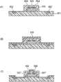
借助引线接合的接线方法如图6所示,是利用由金或铜等形成的直径数10μm左右的引线13来将形成在半导体芯片22上表面的接合垫22a与绝缘基材11侧的电极垫11a彼此连接的方法。更具体而言,所述接线方法是这样的方法:利用超声波并用热压接方式将穿过形成在可移动的毛细管的中心的贯穿孔并从毛细管之顶端突出的引线连接至一个垫之后,一边从贯穿孔抽出引线一边使毛细管移动到另一个垫,向该另一个垫按压引线以及毛细管并通过超声波并用热压接方式将引线连接至垫,同时切断引线。As shown in FIG. 6, the wiring method by wire bonding is to connect the
根据引线接合的方法,如图6所示,利用直径数10μm左右的引线13来将形成在半导体芯片22表面的接合垫22a与绝缘基材11表面的电极垫11a彼此接线。根据此种方法,存在如下所述的问题。According to the wire bonding method, as shown in FIG. 6 , the
通常,在半导体装置的制造工序中,在引线接合工序之后,通过树脂密封材料来密封半导体芯片的表面而实现封装,以保护半导体芯片。在此种密封工序中所用的密封材料中,通常添加有大量的无机填充材料,以赋予充分的绝缘性,或者提高尺寸稳定性。并且,大量含有此种无机填充材料的密封材料的流动性极差。因此,如果要在将搭载有半导体芯片的基材内插到模具内之后,使密封材料完全填充到模具内,则必须在非常高的压力下成型。此种情况下存在如下问题:用于接合的引线会承受较大的外力,引线会切断或损伤,由此损害半导体装置的可靠性。为了解决此类问题,也曾采用了加大引线直径的对策。但是,广泛用于引线的是价格昂贵的金。因此,加大引线直径会导致成本上升。除此以外,在引线接合的方法中,考虑到引线的摇摆(スイ一プ)量而无法缩窄引线的间隔,因此也存在布线密度低的问题。Usually, in the manufacturing process of a semiconductor device, after a wire bonding process, the surface of a semiconductor chip is sealed with a resin sealing material, and packaging is implemented, and a semiconductor chip is protected. A large amount of inorganic filler is usually added to the sealing material used in such a sealing step in order to impart sufficient insulation or to improve dimensional stability. Furthermore, a sealing material containing a large amount of such an inorganic filler has extremely poor fluidity. Therefore, if the sealing material is to be completely filled in the mold after inserting the base material on which the semiconductor chip is inserted into the mold, molding must be performed under very high pressure. In this case, there is a problem that a large external force is applied to the wire used for bonding, and the lead wire is cut or damaged, thereby impairing the reliability of the semiconductor device. In order to solve such problems, a countermeasure of increasing the diameter of the lead wire has also been adopted. However, it is expensive gold that is widely used for wires. Therefore, increasing the diameter of the lead leads to an increase in cost. In addition, in the wire bonding method, the spacing between the wires cannot be narrowed in consideration of the amount of sway of the wires, so there is also a problem of low wiring density.
作为取代引线接合的方法,例如已知的是下述非专利文献1公开的方法。具体说明其概略。(1)首先,利用硅氧化膜来包覆固定在可挠性基板上的半导体芯片。然后,在硅氧化膜表面形成用于平坦化的有机膜。接下来,使用金属掩模,去除半导体芯片表面的接合垫的表面以及可挠性基板上形成的电极垫的表面上的硅氧化膜以及有机膜。(2)然后,仅去除其他部分的有机膜。(3)接下来,使电镀种子附着于整个表面,然后以覆盖电镀种子的方式形成电镀用抗蚀剂。然后,在电镀用抗蚀剂表面进一步形成硅氧化膜。继而,在硅氧化膜表面再形成用于平坦化的有机膜。(4)然后,使用金属掩模,以沿着连接接合垫与电极垫的、要形成布线的部分的路径的方式,去除硅氧化膜以及有机膜。(5)继而,将硅氧化膜作为掩模,去除未形成硅氧化膜的部分的电镀用抗蚀剂,从而使电镀种子露出。(6)最后,实施电镀处理,从而仅在上述工序中残留电镀种子的部分形成电镀层,以形成布线。As a method replacing wire bonding, for example, a method disclosed in
现有技术文献prior art literature
非专利文献1:第19届微电机/MEMS展的同时召开安排“FINE MEMS计划中间成果发表会(2008年7月31日于东京国际展览馆(Tokyo Big Sight))”的“MEMS-半导体横向布线技术(东北大学大学院工学研究科小柳光正氏演讲)”的参考配发物Non-Patent Document 1: "MEMS-Semiconductor Horizontal" "MEMS-Semiconductor Horizontal" was held at the same time as the 19th Micromotor/MEMS Exhibition "FINE MEMS Program Intermediate Results Presentation Conference (July 31, 2008 at Tokyo Big Sight)" Wiring Technology (Lecture by Mitsumasa Koyanagi, Graduate School of Engineering, Tohoku University)" reference distribution
发明内容Contents of the invention
发明要解决的问题The problem to be solved by the invention
本发明想要解决以往为了将配置在绝缘基材表面的半导体芯片连接于形成在绝缘基材表面的电极垫而使用的引线接合中的所述问题,其目的在于,利用容易的工序形成能够抑制借助树脂密封材料进行的密封时的引线的切断或损伤的产生的布线。The present invention intends to solve the above problems in the conventional wire bonding used for connecting a semiconductor chip arranged on the surface of an insulating base material to an electrode pad formed on the surface of an insulating base material. Wiring caused by cutting or damage to lead wires during sealing with a resin sealing material.
而且,本发明的又一目的在于,在表面设有布线的立体结构物中,提高布线相对于该立体结构物的粘合强度,从而减少布线的脱落、偏离、断裂等问题。Furthermore, another object of the present invention is to increase the adhesive strength of the wiring relative to the three-dimensional structure in a three-dimensional structure provided with wiring on the surface, thereby reducing problems such as dropout, deviation, and breakage of the wiring.
解决问题的手段means of solving problems
本发明是一种半导体芯片的安装方法,用于将配置在绝缘基材表面的半导体芯片的表面上所设的接合垫电连接至与形成在所述绝缘基材表面的所述接合垫对应的电极垫,其特征在于,包括:覆膜形成工序,在连接所述接合垫与所述电极垫的路径的表面形成树脂覆膜;布线槽形成工序,沿着用于连接所述接合垫与所述电极垫的路径,通过激光加工而形成深度等于或大于所述树脂覆膜的厚度的布线槽;催化剂沉积工序,使电镀催化剂或其前体沉积在所述布线槽的表面;覆膜去除工序,使所述树脂覆膜溶解或膨润于指定液体以将其去除;以及电镀处理工序,在去除所述树脂覆膜之后,仅在残留所述电镀催化剂或由所述电镀催化剂前体形成的电镀催化剂的部位形成非电解镀膜。The present invention is a semiconductor chip mounting method for electrically connecting bonding pads provided on the surface of a semiconductor chip arranged on the surface of an insulating base material to corresponding bonding pads formed on the surface of the insulating base material. The electrode pad is characterized by comprising: a film forming step of forming a resin film on the surface of a path connecting the bonding pad and the electrode pad; a wiring groove forming step along the path for connecting the bonding pad and the electrode pad. The path of the electrode pad is processed by laser to form a wiring groove with a depth equal to or greater than the thickness of the resin film; the catalyst deposition process is to deposit the electroplating catalyst or its precursor on the surface of the wiring groove; the film removal process, dissolving or swelling the resin coating in a prescribed liquid to remove it; and a plating treatment process of leaving only the electroplating catalyst or the electroplating catalyst precursor formed of the electroplating catalyst after removing the resin coating The catalyst part forms an electroless plating film.
本发明又是一种立体结构物,其在表面设有布线,其特征在于:在立体结构物的表面,形成跨及立体结构物的彼此交叉的相邻面间或者在平面或曲面上延伸的布线用凹槽,将布线用导体的至少一部分埋入所述布线用凹槽中。The present invention is another three-dimensional structure, which is provided with wiring on the surface. In the wiring groove, at least a part of the wiring conductor is buried in the wiring groove.
本发明的目的、方案、特征以及优点,通过以下的详细说明与附图将更为明确。The objects, solutions, features and advantages of the present invention will be clarified by the following detailed description and accompanying drawings.
附图说明Description of drawings
图1(A)~图1(C)是用于说明本发明的第一实施方式所涉及的半导体芯片的安装方法的前半工序的说明图。1(A) to 1(C) are explanatory diagrams for explaining the first half process of the semiconductor chip mounting method according to the first embodiment of the present invention.
图2(A)~图2(C)是用于说明本发明的第一实施方式所涉及的半导体芯片的安装方法的后半工序的说明图。2(A) to 2(C) are explanatory diagrams for explaining the second half process of the semiconductor chip mounting method according to the first embodiment of the present invention.
图3是使用本发明的第一实施方式所涉及的半导体芯片的安装方法所获得的半导体装置的示意说明图。3 is a schematic explanatory diagram of a semiconductor device obtained by using the semiconductor chip mounting method according to the first embodiment of the present invention.
图4(A)~图4(C)是用于说明本发明的第二实施方式所涉及的半导体芯片的连接方法的前半工序的说明图。4(A) to 4(C) are explanatory diagrams for explaining the first-half process of the method for connecting semiconductor chips according to the second embodiment of the present invention.
图5(A)~图5(C)是用于说明本发明的第二实施方式所涉及的半导体芯片的连接方法的后半工序的说明图。5(A) to 5(C) are explanatory diagrams for explaining the second-half process of the semiconductor chip connection method according to the second embodiment of the present invention.
图6是示意性地表示通过引线接合的方法而接线的以往的半导体装置的安装结构的示意图。FIG. 6 is a schematic view schematically showing a mounting structure of a conventional semiconductor device connected by wire bonding.
图7是表示利用非专利文献1所公开的方法而获得的立体布线在基材表面上的状态的说明图。FIG. 7 is an explanatory view showing a state of three-dimensional wiring obtained by the method disclosed in Non-Patent
图8(A)~图8(E)是形成深度等于树脂覆膜的厚度的布线槽时的、与图1(B)~图1(C)或者图4(B)~图4(C)以及图2(A)~图2(C)或者图5(A)~图5(C)对应的工序图。Figures 8(A) to 8(E) are the same as those shown in Figures 1(B) to 1(C) or Figures 4(B) to 4(C) when forming wiring grooves with a depth equal to the thickness of the resin film. And Fig. 2(A)-Fig. 2(C) or Fig. 5(A)-Fig. 5(C) corresponding process diagrams.
图9(A)~图9(E)是形成深度大于树脂覆膜的厚度的布线槽时的、与图1(B)~图1(C)或者图4(B)~图4(C)以及图2(A)~图2(C)或者图5(A)~图5(C)对应的工序图。Figs. 9(A) to 9(E) are the same as Figs. 1(B) to 1(C) or Figs. And Fig. 2(A)-Fig. 2(C) or Fig. 5(A)-Fig. 5(C) corresponding process diagrams.
图10(a)~图10(c)是表示图9(E)中所得的布线的变形例的说明图。10( a ) to 10( c ) are explanatory diagrams showing modifications of the wiring obtained in FIG. 9(E) .
图11(A)~图11(C)是表示使用CMP处理的布线形成方法的工序图。11(A) to 11(C) are process diagrams showing a wiring formation method using CMP processing.
图12是表示本发明的第三实施方式所涉及的在表面设有布线的立体结构物的主要部分的放大立体图。12 is an enlarged perspective view showing a main part of a three-dimensional structure provided with wiring on a surface according to a third embodiment of the present invention.
图13是表示所述立体结构物中的垫部的结构的具体一例的放大剖视图。Fig. 13 is an enlarged cross-sectional view showing a specific example of the structure of a pad portion in the three-dimensional structure.
图14(a)是表示所述立体结构物中的垫部结构的不理想例的放大剖视图,图14(b)是表示理想例的放大剖视图。Fig. 14(a) is an enlarged cross-sectional view showing an unideal example of the pad structure in the three-dimensional structure, and Fig. 14(b) is an enlarged cross-sectional view showing an ideal example.
图15是表示本发明的第四实施方式所涉及的在表面设有布线的立体结构物的主要部分的放大立体图。15 is an enlarged perspective view showing a main part of a three-dimensional structure provided with wiring on a surface according to a fourth embodiment of the present invention.
图16是表示本发明的第五实施方式所涉及的在表面设有布线的立体结构物(安装在绝缘基材上的半导体芯片被绝缘性树脂包覆的半导体装置)的剖视图。16 is a cross-sectional view showing a three-dimensional structure (semiconductor device in which a semiconductor chip mounted on an insulating base material is covered with an insulating resin) provided with wiring on the surface according to a fifth embodiment of the present invention.
图17(A)~图17(C)是用于说明所述第五实施方式所涉及的立体结构物的制法的前半工序的剖视图。17(A) to 17(C) are sectional views for explaining the first half process of the manufacturing method of the three-dimensional structure according to the fifth embodiment.
图18(A)~图18(C)是用于说明所述第五实施方式所涉及的立体结构物的制法的后半工序的剖视图。18(A) to 18(C) are cross-sectional views for explaining the second half step of the method of manufacturing the three-dimensional structure according to the fifth embodiment.
图19(a)~图19(c)是表示本发明的第六实施方式所涉及的在表面设有布线的立体结构物(安装在绝缘基材上的半导体芯片被绝缘性树脂包覆的半导体装置)的彼此不同的例子的剖视图。19(a) to 19(c) show a three-dimensional structure with wiring on the surface (semiconductor chip mounted on an insulating base material covered with an insulating resin) according to a sixth embodiment of the present invention. Cross-sectional views of mutually different examples of devices).
图20是表示作为本发明的第七实施方式所涉及的在表面设有布线的立体结构物(安装在绝缘基材上的半导体芯片被绝缘性树脂包覆的半导体装置)的具体1例的存储卡的剖视图。20 is a storage diagram showing a specific example of a three-dimensional structure with wiring on its surface (a semiconductor device in which a semiconductor chip mounted on an insulating base material is covered with an insulating resin) according to the seventh embodiment of the present invention. Cutaway view of the card.
图21是表示作为本发明的第八实施方式所涉及的在表面设有布线的立体结构物(被动元件被绝缘性树脂包覆的电子器件)的具体1例的磁头的剖视图。21 is a cross-sectional view showing a magnetic head as a specific example of a three-dimensional structure (electronic device in which passive elements are covered with an insulating resin) provided with wiring on the surface according to the eighth embodiment of the present invention.
具体实施方式Detailed ways
根据本发明人等的研究,根据非专利文献1公开的方法,不使用引线接合,而形成连接基板表面的电极垫与芯片表面的接合垫的布线。但是,此种方法需要复杂的多个工序,因为被认为不适合于量产化。本发明是基于此种研究的结果而完成。以下,对用于实施本发明的形态进行详细说明。According to studies by the present inventors, according to the method disclosed in
(第一实施方式)(first embodiment)
参照附图,对本发明所涉及的半导体芯片的安装方法的理想实施方式进行说明。Preferred embodiments of the semiconductor chip mounting method according to the present invention will be described with reference to the drawings.
图1以及图2是用于说明本实施方式的半导体芯片的安装方法的各工序的示意图。另外,图1以及图2中,1为绝缘基材,1a为电极垫,2为半导体芯片,2a为接合垫,3为树脂覆膜,4为布线槽,5为电镀催化剂,6为非电解镀膜,7为布线。1 and 2 are schematic diagrams for explaining each step of the semiconductor chip mounting method according to the present embodiment. 1 and 2, 1 is an insulating substrate, 1a is an electrode pad, 2 is a semiconductor chip, 2a is a bonding pad, 3 is a resin coating, 4 is a wiring groove, 5 is an electroplating catalyst, 6 is an electrolytic Coating, 7 is wiring.
在本实施方式的制造方法中,如图1(A)所示,首先准备在指定的芯片搭载区域配置有半导体芯片2的绝缘基材1。In the manufacturing method of this embodiment, as shown in FIG. 1(A), first, an insulating
另外,半导体芯片2通过粘合剂等而固接于绝缘基材1表面的指定的芯片搭载区域,粘合面以不残留间隙的方式而由树脂所填埋。另外,由后文可明确的是,为了避免在半导体芯片2的硅晶片(尤其是其切割的侧面)上直接形成由非电解镀膜6构成的布线7,例如更理想的是,利用树脂等绝缘性有机材料或以二氧化硅(SiO2)等为首的陶瓷等绝缘性无机材料等,至少预先包覆形成所述布线7的半导体芯片2的部分。In addition, the
作为半导体芯片,并无特别限定,可使用IC(Integrated Circuit,集成电路)、LSI(Large Scale Integration,大规模集成电路)、VLSI(Very Large Scale Integration,超大规模集成电路)、LED芯片等发光半导体芯片等。As a semiconductor chip, there is no special limitation, and light-emitting semiconductors such as IC (Integrated Circuit, integrated circuit), LSI (Large Scale Integration, large-scale integration), VLSI (Very Large Scale Integration, very large-scale integration), and LED chips can be used. chips etc.
并且,如图1(B)所示,在半导体芯片2以及绝缘基材1的表面形成树脂覆膜3(覆膜形成工序)。Then, as shown in FIG. 1(B), a resin coating 3 is formed on the surfaces of the
作为绝缘基材1,并无特别限定,可使用一直以来用于半导体芯片的安装的各种有机基材或无机基材。作为有机基材的具体例,可列举由环氧树脂、丙烯树脂、聚碳酸酯树脂、聚酰亚胺树脂、聚苯硫醚树脂等构成的基材。作为基材形态,并无特别限定,可为片材、薄膜、预浸料坯、三维形状的成型体等。绝缘基材1的厚度无特别限定。在片材、薄膜、或者预浸料坯的情况下,例如较为理想的是10~200μm,更理想的是20~100μm左右。The insulating
树脂覆膜3的形成方法并无特别限定,只要是至少在绝缘基材1的表面以及半导体芯片2的表面,在连接各电极垫1a、1a与各接合垫2a、2a的路径的表面形成树脂覆膜3的方法即可。具体而言,例如可列举通过以下的方法等而形成的方法,即:如图1(B)所示,在绝缘基材1的配置半导体芯片2的面的整个面上,涂敷可形成树脂覆膜3的液状材料之后使其干燥。另外,作为其他方法,还可列举将预先形成在支撑基材上的树脂覆膜3转印到绝缘基材1表面的方法。涂敷树脂液时的方法并无特别限定。具体而言,可使用浸涂法或喷涂法等。The method of forming the resin film 3 is not particularly limited, as long as the resin is formed on at least the surface of the insulating
作为树脂覆膜3的厚度,较为理想的是10μm以下,更理想的是5μm以下且0.1μm以上,进而理想的是1μm以上。如果厚度过厚,则存在通过激光加工局部去除树脂覆膜3时尺寸精度会下降的倾向。而且,如果厚度过薄,则存在难以形成均匀膜厚的覆膜的倾向。The thickness of the resin coating 3 is preferably not more than 10 μm, more preferably not more than 5 μm and not less than 0.1 μm, and still more preferably not less than 1 μm. If the thickness is too thick, the dimensional accuracy tends to decrease when the resin coating 3 is partially removed by laser processing. Furthermore, if the thickness is too thin, it tends to be difficult to form a coating with a uniform thickness.
作为用于形成树脂覆膜3的材料,只要是在后述的去除工序中可溶解去除或膨润去除的树脂材料即可,可无特别限定地使用。具体而言,例如,可使用在光致抗蚀剂的领域中使用的抗蚀剂树脂、或对指定液体的膨润度高而可通过膨润而剥离的树脂。As a material for forming the resin film 3 , any resin material can be used without particular limitation as long as it is a resin material that can be removed by dissolution or swelling in a removal step described later. Specifically, for example, a resist resin used in the field of photoresists, or a resin that has a high swelling degree to a predetermined liquid and can be peeled off by swelling can be used.
作为抗蚀剂树脂的具体例,例如可列举光固化性环氧树脂、蚀刻抗蚀剂、聚酯类树脂、松香类树脂。Specific examples of resist resins include, for example, photocurable epoxy resins, etching resists, polyester resins, and rosin resins.
而且,作为膨润性树脂,较为理想的是对指定液体的膨润度为50%以上,更理想的是100%以上,进而理想的是500%以上的膨润性树脂。作为此种树脂的具体例,例如可列举通过调整交联度或凝胶化度等而调整成所需膨润度的苯乙烯-丁二烯类共聚物等二烯类弹性体、丙烯酸酯类共聚物等丙烯类弹性体、以及聚酯类弹性体等。Furthermore, the swelling resin preferably has a degree of swelling with respect to a predetermined liquid of 50% or more, more preferably 100% or more, and still more preferably 500% or more. Specific examples of such resins include diene-based elastomers such as styrene-butadiene-based copolymers, acrylate-based elastomers, and styrene-butadiene-based copolymers whose swelling degree is adjusted to a desired degree of swelling by adjusting the degree of crosslinking or gelation. Propylene-based elastomers such as copolymers, polyester-based elastomers, etc.
对于树脂覆膜3,再次详细追加说明。The resin coating 3 will be described again in detail.
作为树脂覆膜(抗蚀剂)3,并无特别限定,只要可在后述的去除工序中去除即可。树脂覆膜3较为理想的是可通过在指定液体中溶解或者膨润而从绝缘基材1的表面容易地溶解去除或者剥离去除的树脂覆膜。具体而言,例如可列举由可由有机溶剂或碱溶液容易地溶解的可溶型树脂构成的覆膜、或者由可在指定液体(膨润液)中膨润的膨润性树脂构成的覆膜等。另外,对于膨润性树脂覆膜,不仅包含并不实质溶解于指定液体,但可通过膨润而从绝缘基材1的表面容易地剥离的树脂覆膜,而且还包含可在指定液体中膨润,且至少一部分溶解,且通过该膨润或溶解可从绝缘基材1的表面容易地剥离的树脂覆膜,或可溶解于指定液体,且通过该溶解可从绝缘基材1的表面容易地剥离的树脂覆膜。通过使用此种树脂覆膜,能够从绝缘基材1的表面容易且良好地去除树脂覆膜3。如果在去除树脂覆膜3时破坏了树脂覆膜,则存在以下问题,即沉积在该树脂覆膜3上的电镀催化剂5会飞散,飞散的电镀催化剂会再沉积于绝缘基材1而在该部分形成多余的电镀层。本实施方式中,由于能够从绝缘基材1的表面容易且良好地去除树脂覆膜3,因此能够防患此类问题于未然。The resin coating (resist) 3 is not particularly limited as long as it can be removed in a removal step described later. The resin coating 3 is preferably a resin coating that can be easily dissolved or removed from the surface of the insulating
树脂覆膜3的形成方法并无特别限定。具体而言,例如可列举在绝缘基材1的表面涂敷可形成树脂覆膜3的液状材料之后使其干燥的方法,或者将通过在支撑基材上涂敷所述液状材料之后进行干燥而形成的树脂覆膜转印到绝缘基材1的表面的方法等。而且,作为其他方法,也可列举在绝缘基材1的表面贴合由预先形成的树脂覆膜3构成的树脂薄膜的方法等。另外,作为涂敷液状材料的方法,并无特别限定。具体而言,例如可列举一直以来为人所知的旋涂法或棒涂法等。The method for forming the resin coating 3 is not particularly limited. Specifically, for example, a method of applying a liquid material capable of forming the resin coating 3 on the surface of the insulating
作为用于形成树脂覆膜3的材料,可无特别限定地使用,只要是可通过在指定液体中溶解或者膨润而从绝缘基材1的表面容易地溶解去除或者剥离去除的树脂即可。较为理想的是,使用对指定液体的膨润度达到50%以上,更理想的是达到100%以上,进而理想的是达到500%以上的膨润度的树脂。另外,如果膨润度过低,则存在难以剥离树脂覆膜的倾向。The material for forming the resin film 3 is not particularly limited as long as it is a resin that can be easily dissolved or removed from the surface of the insulating
另外,树脂覆膜的膨润度(SW)是根据膨润前重量m(b)以及膨润后重量m(a),通过“膨润度SW={(m(a)-m(b))/m(b)}×100(%)”的数式而求出。In addition, the swelling degree (SW) of the resin coating is based on the weight before swelling m(b) and the weight after swelling m(a), by "swelling degree SW={(m(a)-m(b) )/m(b)}×100(%)” to obtain it.
此种树脂覆膜3可通过在绝缘基材1的表面涂敷弹性体的悬浮液或者乳状液之后进行干燥的方法,或者将通过在支撑基材上涂敷弹性体的悬浮液或者乳状液之后进行干燥而形成的覆膜转印到绝缘基材1的表面的方法等而容易地形成。This kind of resin film 3 can be dried after coating the suspension or emulsion of the elastomer on the surface of the insulating
作为弹性体的具体例,可列举苯乙烯-丁二烯类共聚物等二烯类弹性体、丙烯酸酯类共聚物等丙烯类弹性体以及聚酯类弹性体等。根据此种弹性体,可通过调整分散为悬浮液或者乳状液的弹性体树脂粒子的交联度或凝胶化度等而容易地形成所需膨润度的树脂覆膜。Specific examples of the elastomer include diene-based elastomers such as styrene-butadiene-based copolymers, propylene-based elastomers such as acrylate-based copolymers, polyester-based elastomers, and the like. According to such an elastomer, it is possible to easily form a resin film having a desired swelling degree by adjusting the degree of crosslinking, the degree of gelation, and the like of the elastomer resin particles dispersed in a suspension or emulsion.
另外,作为此种树脂覆膜3,尤其理想的是膨润度依存于膨润液的pH值而变化的覆膜。当使用此种覆膜时,通过使后述的催化剂沉积工序中的液性条件与后述的覆膜去除工序中的液性条件各异,从而既能在催化剂沉积工序中的pH值下维持树脂覆膜3对绝缘基材1的高密接力,又能在覆膜去除工序中的pH值下容易地从绝缘基材1剥离去除树脂覆膜3。In addition, as such a resin coating 3, a coating whose swelling degree changes depending on the pH value of the swelling liquid is particularly preferable. When using such a coating, by making the liquid conditions in the catalyst deposition process described later different from the liquid conditions in the coating removal process described later, it is possible to maintain the pH value in the catalyst deposition process. The high adhesion of the resin coating 3 to the insulating
更具体而言,例如,当后述的催化剂沉积工序例如具备在pH值为1~3的范围的酸性催化剂金属胶体溶液中进行处理的工序,后述的覆膜去除工序例如具备在pH值为12~14的范围的碱性溶液中使树脂覆膜膨润的工序时,所述树脂覆膜3较为理想的是对所述酸性催化剂金属胶体溶液的膨润度为60%以下,更理想的是40%以下,对所述碱性溶液的膨润度为50%以上,更理想的是100%以上,进而理想的是500%以上的树脂覆膜。More specifically, for example, when the catalyst deposition process described later includes, for example, a process of treating in an acidic catalyst metal colloid solution with a pH value in the range of 1 to 3, the film removal process described later includes, for example, a process where the pH value is In the step of swelling the resin coating in an alkaline solution in the range of 12 to 14, it is preferable that the swelling degree of the resin coating 3 with respect to the acidic catalyst metal colloid solution is 60% or less, more preferably The resin film is 40% or less, and the swelling degree to the alkaline solution is 50% or more, more preferably 100% or more, and more preferably 500% or more.
作为此种树脂覆膜3的例子,可列举由具有指定量的羧基的弹性体形成的片材、对印刷电路板的图案化用的干膜抗蚀剂(以下有时称作“DFR”)等中所用的光固化性的碱性显影型的抗蚀剂进行全面固化所得的片材、及热固性或碱显影型的片材等。Examples of such a resin coating 3 include a sheet made of an elastomer having a predetermined amount of carboxyl groups, a dry film resist (hereinafter sometimes referred to as "DFR") for patterning a printed circuit board, and the like. Sheets obtained by fully curing the photocurable alkali-developing resist used in the film, and thermosetting or alkali-developing sheets.
作为具有羧基的弹性体的具体例,可列举通过包含具有羧基的单体单位来作为共聚成分而在分子中具有羧基的苯乙烯-丁二烯类共聚物等二烯类弹性体、丙烯酸酯类共聚物等丙烯类弹性体、或者聚酯类弹性体等。根据此类弹性体,通过调整分散为悬浮液或者乳状液的弹性体的酸当量、交联度或者凝胶化度等,能够形成具有所需碱膨润度的树脂覆膜。而且,能够进一步增大对在覆膜去除工序中使用的指定液体的膨润度,也能够容易地形成相对于所述液体而溶解的树脂覆膜。弹性体中的羧基发挥使树脂覆膜相对于碱性水溶液而膨润,以从绝缘基材1的表面剥离树脂覆膜3的作用。而且,酸当量是指每1个羧基的聚合物分子量。Specific examples of the elastomer having a carboxyl group include diene-based elastomers such as styrene-butadiene copolymers having a carboxyl group in the molecule by containing a monomer unit having a carboxyl group as a copolymerization component, and acrylate-based elastomers. Propylene-based elastomers such as copolymers, polyester-based elastomers, and the like. According to such an elastomer, by adjusting the acid equivalent, degree of crosslinking, degree of gelation, etc. of the elastomer dispersed as a suspension or emulsion, a resin film having a desired degree of alkali swelling can be formed. Furthermore, it is possible to further increase the degree of swelling with respect to a predetermined liquid used in the film removal step, and it is also possible to easily form a resin film that dissolves in the liquid. The carboxyl group in the elastomer plays the role of causing the resin coating to swell with the alkaline aqueous solution to peel the resin coating 3 from the surface of the insulating
作为具有羧基的单体单位的具体例,可列举(甲基)丙烯酸、反丁烯二酸、肉桂酸、丁烯酸、衣康酸以及马来酸酐等。Specific examples of the monomer unit having a carboxyl group include (meth)acrylic acid, fumaric acid, cinnamic acid, crotonic acid, itaconic acid, and maleic anhydride.
作为此类具有羧基的弹性体中的羧基的含有比例,较为理想的是以酸当量计为100~2000,更为理想的是100~800。如果酸当量过小(羧基的数量相对过多),则与溶剂或其他组成物的相溶性会下降,从而存在对非电解电镀的前处理液的耐受性下降的倾向。而且,如果酸当量过大(羧基的数量相对过少),则存在相对于碱性水溶液的剥离性下降的倾向。As a content ratio of the carboxyl group in the elastomer which has such a carboxyl group, it is preferable that it is 100-2000 in acid equivalent, and it is more preferable that it is 100-800. If the acid equivalent is too small (the number of carboxyl groups is relatively large), the compatibility with solvents or other components decreases, and the resistance to the pretreatment liquid for electroless plating tends to decrease. And when the acid equivalent is too large (the number of carboxyl groups is relatively too small), there exists a tendency for the peelability with respect to alkaline aqueous solution to fall.
而且,作为弹性体的分子量,较为理想的是1万~100万,更为理想的是2万~50万,进而理想的是2万~6万。如果弹性体的分子量过大,则存在剥离性下降的倾向,如果过小,则粘度会下降,因此难以均匀地维持树脂覆膜的厚度,并且存在对非电解电镀的前处理液的耐受性也会下降的倾向。Furthermore, the molecular weight of the elastomer is more preferably 10,000 to 1 million, more preferably 20,000 to 500,000, and still more preferably 20,000 to 60,000. If the molecular weight of the elastomer is too large, the peelability tends to decrease, and if it is too small, the viscosity decreases, so it is difficult to maintain the thickness of the resin coating uniformly, and there is resistance to the pretreatment liquid of electroless plating also tends to decline.
而且,作为DFR,例如可使用将含有指定量的羧基的丙烯类树脂、环氧类树脂、苯乙烯类树脂、酚类树脂、氨基甲酸酯类树脂等作为树脂成分,并含有光聚合引发剂的光固化性树脂组成物的片材。作为此类DFR的具体例,如果要举例,例如可列举使日本专利公开公报特开2000-231190号、日本专利公开公报特开2001-201851号、日本专利公开公报特开平11-212262号中公开的光聚合性树脂组成物的干膜全面固化所得的片材、或作为碱性显影型的DFR而市售的例如旭化成工业公司制的UFG系列等。Furthermore, as the DFR, for example, acrylic resin, epoxy resin, styrene resin, phenol resin, urethane resin, etc. containing a predetermined amount of carboxyl groups can be used as the resin component and contain a photopolymerization initiator. A sheet of a photocurable resin composition. As specific examples of such DFR, for example, Japanese Patent Laid-Open Publication No. 2000-231190, Japanese Patent Laid-Open Publication No. 2001-201851, and Japanese Patent Laid-Open Publication No. Hei 11-212262 can be cited. A sheet obtained by fully curing the dry film of the photopolymerizable resin composition, or a commercially available alkaline-developing DFR such as UFG series manufactured by Asahi Kasei Industries, Ltd.
进而,作为其他树脂覆膜3的例子,可列举含有羧基的以松香为主成分的树脂(例如,吉川化工公司制的“NAZDAR229”)或以苯酚为主成分的树脂(例如,LEKTRACHEM公司制的“104F”)等。Furthermore, examples of other resin coatings 3 include carboxyl group-containing resins mainly composed of rosin (for example, "NAZDAR 229" manufactured by Yoshikawa Chemical Co., Ltd.) or resins mainly composed of phenol (for example, Resins manufactured by LEKTRACHEM Co., Ltd. "104F") etc.
树脂覆膜3可通过利用以往已知的旋涂法或棒涂法等涂敷方式在绝缘基材1的表面涂敷树脂的悬浮液或者乳状液之后进行干燥的方法、或者通过使用真空层压机等将形成在支撑基材上的DFR贴合到绝缘基材1表面之后进行全面固化而容易地形成。The resin film 3 can be coated with a resin suspension or emulsion on the surface of the insulating
而且,作为所述树脂覆膜3,例如较为理想的是还可使用以由具有酸等量(应为当量)为100~800左右的羧基的丙烯类树脂构成的树脂(含羧基丙烯类树脂)为主成分的树脂覆膜。Furthermore, as the resin coating 3, for example, a resin (carboxyl group-containing propylene resin) composed of acrylic resin having carboxyl groups of about 100 to 800 acid equivalents (should be equivalent) may also be preferably used. Resin coating as the main component.
此外,除了上述材料以外,作为所述树脂覆膜3,以下的材料也适合。即,作为构成所述树脂覆膜3的抗蚀剂材料所需的特性,例如可列举(1)在后述的催化剂沉积工序中,对使形成有树脂覆膜3的绝缘基材1浸渍的液体(带电镀核的药液)的耐受性高;(2)能够通过后述的覆膜去除工序,例如使形成有树脂覆膜3的绝缘基材1浸渍在碱中的工序而容易地去除树脂覆膜(抗蚀剂)3;(3)成膜性高;(4)容易实现干膜(DFR)化;以及(5)保存性高等。作为带电镀核的药液,将在后文进行叙述,例如在酸性Pd-Sn胶体催化剂系统的情况下,全部为酸性(例如pH值为1~3)水溶液。而且,在碱性Pd离子催化剂系统的情况下,催化剂赋予活化剂为弱碱性(pH值为8~12),除此以外为酸性。根据以上所述,作为对带电镀核的药液的耐受性,必须能够耐受pH值1~11、理想的是pH值1~12。另外,所谓能够耐受,是指将使抗蚀剂成膜所得到的样品浸渍到药液中时,抗蚀剂的膨润或溶解得到充分抑制,能够发挥作为抗蚀剂的作用。而且,浸渍温度一般为室温~60℃,浸渍时间为1~10分钟,抗蚀剂膜厚为1~10μm左右,但并不限定于此。作为覆膜去除工序中所用的碱剥离的药液,将在后文进行叙述,例如一般是NaOH水溶液或碳酸钠水溶液。其pH值为11~14,较为理想的是pH值为12至14,能够简单地去除抗蚀剂膜。一般而言,在NaOH水溶液浓度为1~10%左右,处理温度为室温~50℃,处理时间为1~10分钟的条件下进行浸渍或喷涂处理,但并不限定于此。由于要在绝缘材料上形成抗蚀剂,因此成膜性也是关键。必须形成无凹陷等的具有均匀性的膜。而且,为了简化制造工序和降低材料损耗等而进行干膜化,但为了确保操作性,薄膜必须具有弯曲性。而且,利用层压机(辊、真空)将干膜化了的抗蚀剂贴附到绝缘材料上。贴附的温度为室温~160℃,压力和时间为任意。这样,在贴附时要求粘接性。因此,干膜化了的抗蚀剂一般采用由载体薄膜、护罩薄膜包夹的三层结构,从而也兼具防止灰尘附着的功能,但并不限定于此。保存性较为理想的是能够在室温下保存,但也需要能够进行冷藏、冷冻下的保存。这样,需要避免在低温时干式薄膜的组成发生分离,或者弯曲性下降而发生破裂。In addition, in addition to the above-mentioned materials, the following materials are also suitable as the resin film 3 . That is, as the characteristics required for the resist material constituting the resin coating 3, for example, (1) in the catalyst deposition step described later, the insulating
基于以上所述的观点,作为所述树脂覆膜3,也可以是通过使(a)在分子中至少具有1个聚合性不饱和基的羧酸或者酸酐的至少1种以上的单体和(b)可与(a)单体聚合的至少1种以上的单体聚合而获得的聚合物树脂、或者包含该聚合物树脂的树脂组成物。作为其公知技术,如果要举例,例如可列举日本专利公开公报特开平7-281437号、日本专利公开公报特开2000-231190号、日本专利公开公报特开2001-201851号等。作为(a)单体的一例,可列举(甲基)丙烯酸、反丁烯二酸、肉桂酸、丁烯酸、衣康酸、马来酸酐、马来酸半酯、丙烯酸丁酯等,也可单独使用或将两种以上组合使用。作为(b)单体的例子,一般为非酸性且在分子中具有(1个)聚合性不饱和基的单体,但并不受此限定。以保持后述的催化剂沉积工序中的耐受性、固化膜的可挠性等各种特性的方式来选择。具体而言,有(甲基)丙烯酸甲酯、(甲基)丙烯酸乙酯、(甲基)丙烯酸异丙酯、(甲基)丙烯酸正丁酯、(甲基)丙烯酸仲丁酯、(甲基)丙烯酸叔丁酯、(甲基)丙烯酸-2-羟基乙酯、(甲基)丙烯酸-2-羟基丙酯类。而且,有乙酸乙烯酯等乙烯醇的酯类或(甲基)丙烯腈、苯乙烯或可聚合的苯乙烯衍生物等。而且,也可以通过仅分子中具有1个上述聚合性不饱和基的羧酸或酸酐的聚合而获得。此外,用于聚合物的单体能够选定具备多个不饱和基的单体,以能够实现三维交联。而且,可向分子骨架中导入环氧基、羟基、胺基、酰胺基、乙烯基等反应性官能基。Based on the viewpoints described above, the resin coating 3 may be formed by combining (a) at least one monomer of carboxylic acid or acid anhydride having at least one polymerizable unsaturated group in its molecule and ( b) A polymer resin obtained by polymerizing at least one monomer capable of being polymerized with (a) monomer, or a resin composition containing the polymer resin. Examples of such known techniques include Japanese Patent Laid-Open No. 7-281437, Japanese Patent Laid-Open No. 2000-231190, and Japanese Patent Laid-Open No. 2001-201851. Examples of (a) monomers include (meth)acrylic acid, fumaric acid, cinnamic acid, crotonic acid, itaconic acid, maleic anhydride, maleic acid half ester, butyl acrylate, and the like. These can be used alone or in combination of two or more. As an example of (b) monomer, it is a monomer which is generally non-acidic and has (1) polymerizable unsaturated group in a molecule|numerator, However, It is not limited to this. It is selected so as to maintain various properties such as durability in a catalyst deposition step described later and flexibility of a cured film. Specifically, there are methyl (meth)acrylate, ethyl (meth)acrylate, isopropyl (meth)acrylate, n-butyl (meth)acrylate, sec-butyl (meth)acrylate, (meth)acrylate Base) tert-butyl acrylate, 2-hydroxyethyl (meth)acrylate, 2-hydroxypropyl (meth)acrylate. Furthermore, there are esters of vinyl alcohol such as vinyl acetate, (meth)acrylonitrile, styrene or polymerizable styrene derivatives, and the like. Furthermore, it can also be obtained by superposition|polymerizing the carboxylic acid or acid anhydride which has only 1 said polymerizable unsaturated group in a molecule|numerator. In addition, the monomer used for the polymer can be selected to have a plurality of unsaturated groups so that three-dimensional crosslinking can be realized. Furthermore, reactive functional groups such as epoxy groups, hydroxyl groups, amine groups, amide groups, and vinyl groups can be introduced into the molecular skeleton.
当树脂中含有羧基时,树脂中所含的羧基的量以酸当量计为100~2000即可,较为理想的是100~800。如果酸当量过低,则与溶剂或其他组成物的相溶性将下降,且对电镀前处理液的耐受性下降。如果酸当量过高,则剥离性会下降。而且,(a)单体的组成比率较为理想的是5~70质量%。When the resin contains a carboxyl group, the amount of the carboxyl group contained in the resin may be 100-2000 in terms of acid equivalent, preferably 100-800. If the acid equivalent is too low, the compatibility with solvents or other components will decrease, and the tolerance to the pre-plating treatment liquid will decrease. When the acid equivalent is too high, peelability will fall. Furthermore, the composition ratio of (a) monomer is preferably 5 to 70% by mass.
树脂组成物也可将所述聚合物树脂作为主树脂(黏合剂树脂)而设为必要成分,并添加寡聚物、单体、填充剂或其他添加剂的至少1种。主树脂可为具备热塑性的线型的聚合物。为了控制流动性、结晶性等,有时也会接枝以进行分支。作为分子量,以重量平均分子量计为1,000~500,000左右,较为理想的是5,000~50,000。如果重量平均分子量小,则膜的弯曲性或带电镀核的药液耐受性(耐酸性)将下降。而且,如果分子量大,则碱剥离性或设为干膜时的贴附性将变差。此外,为了提高带电镀核的药液耐受性或抑制激光加工时的热变形、控制流动,也可导入交联点。In the resin composition, the above polymer resin may be used as an essential component as a main resin (binder resin), and at least one of an oligomer, a monomer, a filler, or other additives may be added. The main resin may be a thermoplastic linear polymer. In order to control fluidity, crystallinity, etc., grafting may also be performed to branch. The molecular weight is about 1,000 to 500,000, preferably 5,000 to 50,000 as a weight average molecular weight. If the weight average molecular weight is small, the flexibility of the film and the chemical solution resistance (acid resistance) of the charged plating core will decrease. Furthermore, when the molecular weight is large, the alkali release property and the sticking property when used as a dry film will deteriorate. In addition, cross-linking points can also be introduced for the purpose of improving the chemical resistance of the electroplating nuclei, suppressing thermal deformation during laser processing, and controlling flow.
作为单体或寡聚物,只要具有对带电镀核的药液的耐受性和能够利用碱来容易地去除,则可为任何单体或寡聚物。而且,为了提高干膜(DFR)的贴附性,作为粘接性赋予材料,可考虑使用可塑剂。此外,为了提高各种耐受性,可考虑添加交联剂。具体而言,有(甲基)丙烯酸甲酯、(甲基)丙烯酸乙酯、(甲基)丙烯酸异丙酯、(甲基)丙烯酸正丁酯、(甲基)丙烯酸仲丁酯、(甲基)丙烯酸叔丁酯、(甲基)丙烯酸-2-羟基乙酯、(甲基)丙烯酸-2-羟基丙酯类。而且,有乙酸乙烯酯等乙烯醇的酯类或(甲基)丙烯腈、苯乙烯或可聚合的苯乙烯衍生物等。而且,也可以通过仅分子中具有1个上述聚合性不饱和基的羧酸或酸酐的聚合而获得。此外,也可包含多官能性不饱和化合物。也可以是上述单体或使单体反应获得的寡聚物中的任一种。除了上述单体以外,也可包含两种以上的其他光聚合性单体。作为单体的例子,有1,6-己二醇二(甲基)丙烯酸酯、1,4-环己二醇二(甲基)丙烯酸酯,而且有聚丙二醇二(甲基)丙烯酸酯、聚乙二醇二(甲基)丙烯酸酯、聚乙二醇聚丙二醇二(甲基)丙烯酸酯等聚亚氧烷基乙二醇二(甲基)丙烯酸酯、2-二(p-对羟基苯基)丙烷二(甲基)丙烯酸酯、甘油三(甲基)丙烯酸酯、二季戊四醇五(甲基)丙烯酸酯、三羟甲基丙烷三缩水甘油醚三(甲基)丙烯酸酯、双酚A二缩水甘油醚三(甲基)丙烯酸酯、2,2-双(4-甲基丙烯酰氧基五乙氧基苯基)丙烷、含有氨基甲酸酯基的多官能(甲基)丙烯酸酯等。也可以是上述单体或使单体反应获得的寡聚物中的任一种。As the monomer or oligomer, any monomer or oligomer may be used as long as it has resistance to a chemical solution for electroplating nuclei and can be easily removed with an alkali. Furthermore, in order to improve the adhesiveness of the dry film (DFR), it is considered to use a plasticizer as an adhesive imparting material. In addition, in order to improve various resistances, it is conceivable to add a cross-linking agent. Specifically, there are methyl (meth)acrylate, ethyl (meth)acrylate, isopropyl (meth)acrylate, n-butyl (meth)acrylate, sec-butyl (meth)acrylate, (meth)acrylate Base) tert-butyl acrylate, 2-hydroxyethyl (meth)acrylate, 2-hydroxypropyl (meth)acrylate. Furthermore, there are esters of vinyl alcohol such as vinyl acetate, (meth)acrylonitrile, styrene or polymerizable styrene derivatives, and the like. Furthermore, it can also be obtained by superposition|polymerizing the carboxylic acid or acid anhydride which has only 1 said polymerizable unsaturated group in a molecule|numerator. In addition, polyfunctional unsaturated compounds may also be included. Any of the above-mentioned monomers or oligomers obtained by reacting monomers may be used. In addition to the above monomers, two or more other photopolymerizable monomers may also be contained. Examples of monomers include 1,6-hexanediol di(meth)acrylate, 1,4-cyclohexanediol di(meth)acrylate, polypropylene glycol di(meth)acrylate, Polyethylene glycol di(meth)acrylate, polyethylene glycol polypropylene glycol di(meth)acrylate, etc. Polyoxyalkylene glycol di(meth)acrylate, 2-bis(p-hydroxyl Phenyl)propane di(meth)acrylate, Glycerin tri(meth)acrylate, Dipentaerythritol penta(meth)acrylate, Trimethylolpropane triglycidyl ether tri(meth)acrylate, Bisphenol A Diglycidyl ether tri(meth)acrylate, 2,2-bis(4-methacryloxypentaethoxyphenyl)propane, polyfunctional (meth)acrylic acid containing carbamate groups Esters etc. Any of the above-mentioned monomers or oligomers obtained by reacting monomers may be used.
填充剂并无特别限定,可列举二氧化硅、氢氧化铝、氢氧化镁、碳酸钙、粘土、高岭土、氧化钛、硫酸钡、氧化铝、氧化锌、滑石、云母、玻璃、钛酸钾、钙硅石、硫酸镁、硼酸铝、有机填充剂等。而且,抗蚀剂的理想厚度可薄至0.1~10μm,因此较为理想的是填充剂大小也较小。可使用平均粒径较小且对粗粒进行切割所得的填充剂,但也可以在分散时进行粉碎,或通过过滤去除粗粒。The filler is not particularly limited, and examples thereof include silica, aluminum hydroxide, magnesium hydroxide, calcium carbonate, clay, kaolin, titanium oxide, barium sulfate, aluminum oxide, zinc oxide, talc, mica, glass, potassium titanate, Wollastonite, magnesium sulfate, aluminum borate, organic fillers, etc. Moreover, the ideal thickness of the resist can be as thin as 0.1 to 10 μm, so it is desirable that the size of the filler is also small. A filler obtained by cutting coarse particles with a small average particle size may be used, but it may also be pulverized during dispersion, or the coarse particles may be removed by filtration.
作为其他添加剂,可列举光聚合性树脂(光聚合引发剂)、聚合抑制剂、着色剂(染料、颜料、发色系颜料)、热聚合引发剂、环氧或氨基甲酸酯等交联剂等。Examples of other additives include photopolymerizable resins (photopolymerization initiators), polymerization inhibitors, colorants (dyes, pigments, chromogenic pigments), thermal polymerization initiators, crosslinking agents such as epoxy and urethane wait.
在接下来要说明的布线槽形成工序中,树脂覆膜3会受到激光加工等,因此必须对抗蚀剂材料赋予能利用激光来消融的消融性。激光加工机例如可选用二氧化碳激光器或准分子激光器、UV-YAG激光器等。这些激光加工机具备各种固有的波长,通过选用相对于该波长UV吸收率高的材料,能够提高生产率。其中,UV-YAG激光器适合于微细加工,激光波长为三次谐波355nm、四次谐波266nm,因此作为抗蚀剂材料(树脂覆膜3的材料),较为理想的是相对于这些波长UV吸收率相对较高。UV吸收率越高,越能干净利落地完成抗蚀剂(树脂覆膜3)的加工,从而实现生产率的提高。而且,并不限于此,也可能有时选用UV吸收率相对较低的抗蚀剂材料较好。UV吸收率越低,UV光越能透过抗蚀剂(树脂覆膜3),因此能够使UV能量集中于其下的绝缘基材1的加工,例如在绝缘基材1为难以加工的材料时能够获得尤其理想的结果。这样,较为理想的是,根据抗蚀剂(树脂覆膜3)的激光加工的容易度、绝缘基材1的激光加工的容易度以及它们的关系等来设计抗蚀剂材料。In the wiring groove forming step described next, since the resin film 3 is subjected to laser processing or the like, it is necessary to impart ablation properties that can be ablated by laser light to the resist material. As the laser processing machine, for example, carbon dioxide laser, excimer laser, UV-YAG laser, etc. can be selected. These laser processing machines have various unique wavelengths, and productivity can be improved by selecting a material with a high UV absorption rate for the wavelength. Among them, UV-YAG laser is suitable for microfabrication, and the laser wavelength is 355nm of the third harmonic and 266nm of the fourth harmonic. Therefore, as a resist material (material for the resin coating 3), it is ideal to absorb UV light at these wavelengths. rate is relatively high. The higher the UV absorption rate, the more cleanly the processing of the resist (resin film 3 ) can be completed, thereby improving productivity. Moreover, it is not limited thereto, and it may sometimes be better to select a resist material with a relatively low UV absorption rate. The lower the UV absorption rate, the more UV light can pass through the resist (resin coating 3), so it is possible to concentrate the UV energy on the underlying insulating
接下来,如图1(C)所示,形成深度等于或大于所形成的树脂覆膜3的厚度的布线槽4(布线槽形成工序)。布线槽4是沿着用于连接半导体芯片2的表面的各接合垫2a、2a和与各接合垫2a、2a连接的形成在绝缘基材1表面的各电极垫1a、1a的路径,通过激光加工而形成。Next, as shown in FIG. 1(C), a
这样,沿着用于连接各接合垫2a、2a和各电极垫1a、1a的路径形成布线槽4。通过以此方式形成布线槽4,在随后的工序中,仅对形成有布线槽4的部分的表面赋予非电解镀膜6而形成布线。In this way, the
接下来,如图2(A)所示,使电镀催化剂5沉积在形成有布线槽4的表面(催化剂沉积工序)。Next, as shown in FIG. 2(A), the
电镀催化剂5是为了在后述的电镀处理工序中仅在要形成非电解镀膜6的部分形成电镀膜而赋予的催化剂。作为电镀催化剂,并无特别限定,只要使用作为非电解电镀用的催化剂而已知的催化剂即可。而且,也可预先沉积电镀催化剂的前体,在去除树脂覆膜3后生成电镀催化剂。作为电镀催化剂的具体例,例如可列举金属钯(Pd)、铂(Pt)、银(Ag)等或生成这些金属的前体等。The
作为使电镀催化剂5沉积的方法,例如可列举利用在pH值为1~3的酸性条件下经过处理的酸性Pd-Sn胶体溶液进行处理之后,利用酸溶液来进行处理的方法。更具体而言,可列举如下方法。首先,浸渍到界面活性剂的溶液(清洁剂·调节剂)中,对附着在形成有布线槽4的部分的表面上的油分等进行热清洗。接下来,根据需要,利用过硫酸钠-硫酸类的软性蚀刻剂来进行软性蚀刻处理。然后,在pH值为1~2的硫酸水溶液或盐酸水溶液等酸性溶液中进一步进行酸洗。接下来,浸渍到以浓度为0.1%左右的氯化亚锡水溶液等为主成分的预浸液中吸附氯化亚锡之后,进一步浸渍到含有氯化亚锡和氯化钯的pH值为1~3的酸性Pd-Sn胶体等酸性催化剂金属胶体溶液中,从而使Pd以及Sn凝聚并吸附。继而,使吸附的氯化亚锡与氯化钯之间引起氧化还原反应(SnCl2+PdCl2→SnCl4+Pd↓)。从而使作为电镀催化剂的金属钯析出。As a method of depositing the
另外,作为酸性催化剂金属胶体溶液,可使用公知的酸性Pd-Sn胶体催化剂溶液等,也可使用利用了酸性催化剂金属胶体溶液的市售的电镀工艺。此种工艺例如由Rohm andHaas电子材料公司系统化并销售。In addition, as the acid catalyst metal colloid solution, a known acid Pd—Sn colloid catalyst solution or the like can be used, and a commercially available electroplating process using an acid catalyst metal colloid solution can also be used. Such a process is systemized and marketed, for example, by Rohm and Haas Electronic Materials.
通过此种催化剂沉积处理,如图2(A)所示,使电镀催化剂5沉积在布线槽4的表面以及树脂覆膜3的表面。By such a catalyst deposition process, as shown in FIG. 2(A), the
接下来,如图2(B)所示,使树脂覆膜3在指定液体中溶解或膨润,从而从绝缘基材1以及半导体芯片2的表面去除所述树脂覆膜3(覆膜去除工序)。根据该工序,能够使电镀催化剂5仅残留在绝缘基材1以及半导体芯片2的表面的形成有布线槽4的部分的表面。另一方面,沉积在形成有布线槽4的部分以外的树脂覆膜3的表面上的电镀催化剂5在去除树脂覆膜3时被去除。Next, as shown in FIG. 2(B), the resin coating 3 is dissolved or swelled in a predetermined liquid, thereby removing the resin coating 3 from the surfaces of the insulating
作为使树脂覆膜3膨润去除或溶解去除的方法,可列举将树脂覆膜3在指定的膨润液或溶解液中浸渍指定时间的方法。而且,为了提高剥离性或溶解性,尤其理想的是在浸渍过程中照射超声波。另外,在膨润剥离的情况下,也可视需要以轻微的力来进行抽剥。As a method of removing the resin coating 3 by swelling or dissolving, there may be mentioned a method of immersing the resin coating 3 in a predetermined swelling liquid or a dissolving liquid for a predetermined time. Furthermore, in order to improve peelability or solubility, it is especially desirable to irradiate ultrasonic waves during the dipping process. In addition, in the case of swelling peeling, peeling may be performed with a slight force as needed.
作为使树脂覆膜3溶解或者膨润的液体,并无特别限定,只要使用不会使绝缘基材1以及电镀催化剂5实质上分解或溶解,而使树脂覆膜3容易地溶解或者膨润剥离的液体即可。具体而言,当使用光固化性环氧树脂来作为抗蚀剂树脂时,使用有机溶剂或者碱性水溶液的抗蚀剂去除剂等。而且,作为膨润性树脂,当使用例如二烯类弹性体、丙烯类弹性体以及聚酯类弹性体之类的弹性体时,例如较为理想的是使用1~10%左右的浓度的氢氧化钠水溶液等碱性水溶液。The liquid that dissolves or swells the resin coating 3 is not particularly limited as long as the resin coating 3 is easily dissolved or swollen and peeled off without decomposing or dissolving the insulating
而且,作为树脂皮膜(应为覆膜)3,当为通过使(a)在分子中至少具有1个聚合性不饱和基的羧酸或者酸酐的至少1种以上的单体和(b)可与(a)单体聚合的至少1种以上的单体聚合而获得的聚合物树脂、或者包含该聚合物树脂的树脂组成物时,或者在由前述的含羧基丙烯类树脂所形成时,例如较为理想的是可使用1~10%左右的浓度的氢氧化钠水溶液等碱性水溶液。Furthermore, as the resin film (should be a coating) 3, when it is obtained by making (a) at least one monomer of carboxylic acid or acid anhydride having at least one polymerizable unsaturated group in the molecule and (b) In the case of a polymer resin obtained by polymerizing at least one or more monomers polymerized with the (a) monomer, or a resin composition containing the polymer resin, or when formed from the aforementioned carboxyl group-containing propylene resin, for example Preferably, an alkaline aqueous solution such as an aqueous sodium hydroxide solution having a concentration of about 1 to 10% can be used.
另外,当在催化剂沉积工序中使用在如上所述的酸性条件下进行处理的电镀工艺时,较为理想的是,树脂皮膜(应为覆膜)3由在酸性条件下膨润度为60%以下,较为理想的是40%以下,在碱性条件下膨润度为50%以上的例如二烯类弹性体、丙烯类弹性体以及聚酯类弹性体之类的弹性体所形成;或者由通过使(a)在分子中具有至少1个聚合性不饱和基的羧酸或者酸酐的至少1种以上的单体和(b)可与(a)单体聚合的至少1种以上的单体聚合而获得的聚合物树脂或者包含该聚合物树脂的树脂组成物所形成;或者由前述的含羧基丙烯类树脂所形成。此类树脂皮膜(应为覆膜)通过浸渍在pH值为11~14,较为理想的是pH值为12~14的碱性水溶液,例如1~10%左右的浓度的氢氧化钠水溶液等中,而容易地溶解或者膨润,并溶解去除或者剥离去除。另外,为了提高溶解性或者剥离性,也可在浸渍过程中照射超声波。而且,也可视需要通过以轻微的力来抽剥而去除。In addition, when using the electroplating process that is treated under acidic conditions as described above in the catalyst deposition process, it is desirable that the resin film (should be a coating) 3 has a swelling degree of 60% or less under acidic conditions. , more ideally 40% or less, under alkaline conditions, the swelling degree is more than 50% such as diene elastomers, propylene elastomers and polyester elastomers; or formed by polymerizing (a) at least one monomer of carboxylic acid or acid anhydride having at least one polymerizable unsaturated group in the molecule and (b) at least one monomer polymerizable with (a) monomer The obtained polymer resin is either formed of a resin composition containing the polymer resin or formed of the aforementioned carboxyl group-containing propylene resin. This type of resin film (should be a coating) is immersed in an alkaline aqueous solution with a pH value of 11 to 14, preferably an alkaline aqueous solution with a pH value of 12 to 14, such as an aqueous sodium hydroxide solution with a concentration of about 1 to 10%. , and easily dissolves or swells, and dissolves and removes or peels off. In addition, ultrasonic waves may be irradiated during the dipping process in order to improve solubility or releasability. Furthermore, it can also be removed by peeling with a slight force if necessary.
另外,通过使树脂覆膜预先含有荧光性物质,可在上述覆膜去除工序之后,使用通过对检查对象面照射紫外光或近紫外光而引起的来自荧光性物质的发光来检查覆膜去除不良(检查工序)。在本实施方式中,可形成布线宽度极窄的金属布线。在此种情况下,有相邻的金属布线间的树脂覆膜未被完全去除而残留的危险。如果在金属布线间残留有树脂覆膜,则会在该部分形成电镀膜,从而可能成为短路的原因。此种情况下,使树脂覆膜3预先含有荧光性物质,在覆膜去除工序之后,对覆膜去除面照射指定的发光源,通过荧光性物质来使仅残留有覆膜的部分发光,从而能够检查有无覆膜去除不良或覆膜去除不良的部位。In addition, by preliminarily containing a fluorescent substance in the resin coating, after the above-mentioned coating removal process, it is possible to inspect the defective coating removal by using the light emission from the fluorescent substance caused by irradiating the surface to be inspected with ultraviolet light or near ultraviolet light. (Inspection process). In this embodiment mode, metal wiring with an extremely narrow wiring width can be formed. In this case, the resin film between adjacent metal wirings may not be completely removed and may remain. If the resin film remains between the metal wirings, a plated film will be formed on this part, which may cause a short circuit. In this case, the resin coating 3 is made to contain a fluorescent substance in advance, and after the coating removal process, a predetermined light source is irradiated on the coating removal surface, and only the part where the coating remains is made to emit light by the fluorescent substance, thereby It is possible to check whether there is poor film removal or a site with poor film removal.
可含在树脂覆膜3中的荧光性物质并不特别限定,只要是利用指定光源来照射光而展现出发光特性的物质即可。作为其具体例,例如可列举Fluoresceine、Eosine、PyronineG等。The fluorescent substance that can be contained in the resin coating 3 is not particularly limited, as long as it is a substance that exhibits light-emitting characteristics when irradiated with light by a predetermined light source. As its specific example, Fluoresceine, Eosine, PyronineG etc. are mentioned, for example.
通过本检查工序检测到来自荧光性物质的发光的部分是残留树脂覆膜3的部分。因而,通过去除检测到发光的部分,能够抑制在该部分形成电镀膜。由此,能够抑制短路的发生于未然。The portion where light emission from the fluorescent substance is detected in this inspection step is the portion where the resin coating 3 remains. Therefore, by removing the portion where light emission is detected, it is possible to suppress the formation of a plating film on this portion. Thereby, occurrence of a short circuit can be suppressed before it happens.
接下来,如图2(C)所示,仅在残留电镀催化剂5的部位形成非电解镀膜6(电镀处理工序)。通过此种工序,能够使非电解镀膜6仅在形成有布线槽4的部分析出。通过此种非电解镀膜6,形成用于电连接各电极垫1a、1a和半导体芯片2表面的多个各接合垫2a、2a的布线7。Next, as shown in FIG. 2(C), an
作为非电解电镀处理的方法,可使用如下方法,将沉积有电镀催化剂5且配置有半导体芯片2的绝缘基材1浸渍到非电解电镀液的槽中,使非电解镀膜6仅在沉积有电镀催化剂5的部分析出。As a method of electroless plating treatment, the following method can be used, the insulating
作为用于非电解电镀的金属,可列举铜(Cu)、镍(Ni)、钴(Co)、铝(Al)等。这些金属中,以Cu为主成分的电镀的导电性优异,因而较为理想。而且,如果含有Ni,则耐蚀性或与焊锡的密接性优异,因而较为理想。Copper (Cu), nickel (Ni), cobalt (Co), aluminum (Al) etc. are mentioned as a metal used for electroless plating. Among these metals, plating mainly composed of Cu is preferable because of its excellent electrical conductivity. Moreover, when Ni is contained, it is excellent in corrosion resistance and adhesiveness with solder, so it is preferable.
通过此种电镀处理,非电解镀膜6仅在连接各接合垫2a、2a和各电极垫1a、1a的路径表面的残留电镀催化剂5的部分析出。由此,形成连接各接合垫2a、2a和各电极垫1a、1a的布线7。另外,未形成布线槽4的部分受树脂覆膜3保护而不会沉积电镀催化剂5,因此非电解镀膜6不会析出。因而,即使在形成细的布线的情况下,也不会在相邻的布线间残留多余的电镀膜,从而可抑制短路等。By such plating treatment, the electroless plated
另外,用于布线的电镀膜的形成也可仅使用如上所述的非电解电镀的工序而形成厚膜的电镀膜,但为了缩短工序的周期时间,也可并用公知的电解电镀(电解电镀工序)。具体而言,例如,在电解电镀槽中,使阳极侧与在上述工序中形成的非电解镀膜导通,使电流流经与阴极侧电极之间,从而使形成有非电解镀膜6的部分厚膜化。根据此种方法,由于缩短了厚膜化的时间,因此可缩短电镀膜的形成所需的时间。In addition, the formation of the plated film for wiring can also use only the process of electroless plating as described above to form a plated film with a thick film, but in order to shorten the cycle time of the process, it is also possible to use the known electrolytic plating (electrolytic plating process) in combination. ). Specifically, for example, in the electrolytic plating tank, the anode side is connected to the electroless plating film formed in the above process, and an electric current is made to flow between the electrodes on the cathode side, thereby making the part where the
以此方式形成的电镀膜的膜厚并无特别限定,具体而言,例如较为理想的是0.1~10μm,更为理想的是1~5μm左右。The film thickness of the plated film formed in this way is not particularly limited, but specifically, for example, it is preferably about 0.1 to 10 μm, more preferably about 1 to 5 μm.
经过此种工序,如图2(C)所示,在绝缘基材1的表面形成安装半导体芯片2的结构体。Through such a process, as shown in FIG. 2(C), a structure in which the
以此方式在绝缘基材1表面安装半导体芯片2而构成的结构体为了保护其表面,较为理想的是使用内插成型等方法进行树脂密封。此种密封并无特别限定,可使用一直以来所用的半导体装置的制造工艺中的密封方法。In order to protect the surface of the structure formed by mounting the
图3表示利用密封材料8来对通过上述工序将半导体芯片2的所有接合垫2a、2a、......连接于电极垫1a、1a、......而获得的结构体10进行密封所得的半导体装置20的说明图。如图3所示,在结构体10中,在绝缘基材1的表面配设有半导体芯片2。并且,设在半导体芯片2表面的多个接合垫2a、2a、......分别连接于利用由电镀膜构成的布线7而形成在绝缘基材1表面的电极垫1a、1a、......。布线7以顺着半导体芯片2的侧面以及绝缘基材1的表面的方式而形成。因此,即使在将结构体10内插到模具内并进行树脂密封而制造半导体装置20的情况下,也不会对布线施加较大的力。因而,在通过引线接合而接线的结构体中不会产生对引线施加负荷的现象。3 shows a structure 10 obtained by using a sealing material 8 to connect all the
(第二实施方式)(second embodiment)
参照附图,对本发明所涉及的多个半导体芯片的连接方法的理想实施方式进行说明。另外,各工序与第一实施方式中说明的工序同样,因此省略关于重复部分的详细说明。而且,标注与第一实施方式的符号相同的符号的部分是同样的部分,因此省略说明。Preferred embodiments of a method for connecting a plurality of semiconductor chips according to the present invention will be described with reference to the drawings. In addition, since each process is the same as the process demonstrated in 1st Embodiment, detailed description about an overlapping part is abbreviate|omitted. In addition, since the part attached|subjected with the same code|symbol as that of 1st Embodiment is the same part, description is abbreviate|omitted.
图4以及图5是用于说明本实施方式的多个半导体芯片的连接方法的各工序的示意图。另外,图4以及图5中,1为绝缘基材,2为第1半导体芯片,12为第2半导体芯片,2a、12a为接合垫,3为树脂覆膜,4为布线槽,5为电镀催化剂,6为非电解镀膜。4 and 5 are schematic diagrams for explaining each step of the method for connecting a plurality of semiconductor chips according to the present embodiment. 4 and 5, 1 is an insulating base material, 2 is a first semiconductor chip, 12 is a second semiconductor chip, 2a, 12a are bonding pads, 3 is a resin coating, 4 is a wiring groove, 5 is an electroplating Catalyst, 6 is electroless coating.
在本实施方式的制造方法中,如图4(A)所示,首先准备在指定的芯片搭载区域配置有第1半导体芯片2以及第2半导体芯片12的绝缘基材1。In the manufacturing method of this embodiment, as shown in FIG. 4(A), first, an insulating
另外,第1半导体芯片2以及第2半导体芯片12通过粘合剂等而固接于绝缘基材1表面的指定的芯片搭载区域,粘合面以不残留间隙的方式而由树脂所填埋。另外,此时,为了避免在半导体芯片2、12的硅晶片(尤其是其切割的侧面)上直接形成由非电解镀膜6构成的布线17,例如更理想的是,利用树脂等绝缘性有机材料或以二氧化硅(SiO2)等为首的陶瓷等绝缘性无机材料等,至少预先包覆形成所述布线17的半导体芯片2、12的部分。In addition, the
然后,如图1(B)所示,在第1半导体芯片2、及第2半导体芯片12以及绝缘基材1的表面形成树脂覆膜3(皮膜(应为覆膜)形成工序)。Then, as shown in FIG. 1(B), a resin coating 3 is formed on the surfaces of the
树脂覆膜3的形成方法并无特别限定,只要是至少对于绝缘基材1的表面以及第1半导体芯片2、以及第2半导体芯片12的表面,在连接接合垫2a、2a和接合垫12a、12a的路径的绝缘基材1以及半导体芯片2、12的表面形成树脂覆膜3的方法即可。The method of forming the resin film 3 is not particularly limited, as long as it is at least for the surface of the insulating
接下来,如图4(C)所示,形成深度等于或大于所形成的树脂覆膜3的厚度的布线槽4(布线槽形成工序)。布线槽4是沿着用于连接第1半导体芯片2表面的接合垫2a、2a和第2半导体芯片12表面的接合垫12a、12a的路径,通过激光加工而形成。Next, as shown in FIG. 4(C), a
这样,沿着用于连接接合垫2a、2a和接合垫12a、12a的路径而形成布线槽4。通过以此方式形成布线槽4,在随后的工序中,仅对形成有布线槽4的部分的表面赋予非电解镀膜6而形成布线。In this way, the
接下来,如图5(A)所示,使电镀催化剂5沉积在至少形成有布线槽4的表面(催化剂沉积工序)。通过此种催化剂沉积处理,使电镀催化剂5沉积在布线槽4的表面以及树脂覆膜3的表面。Next, as shown in FIG. 5(A), the
接下来,如图5(B)所示,通过使树脂覆膜3在指定液体中溶解或膨润,从绝缘基材1、第1半导体芯片2以及第2半导体芯片12的表面去除树脂覆膜3(覆膜去除工序)。根据该工序,能够使电镀催化剂5仅残留在绝缘基材1、第1半导体芯片2以及第2半导体芯片12表面的形成有布线槽4的部分的表面。另一方面,沉积在形成有布线槽4的部分以外的表面上的电镀催化剂5在去除树脂覆膜3时被去除。Next, as shown in FIG. 5(B), the resin coating is removed from the surfaces of the insulating
接下来,如图5(C)所示,仅在残留电镀催化剂5的部位形成非电解镀膜6(电镀处理工序)。通过此种工序,使非电解镀膜6仅在形成有布线槽4的部分析出。通过此种非电解镀膜6,形成用于电连接接合垫2a、2a和接合垫12a、12a的布线17。Next, as shown in FIG. 5(C), an
通过此种电镀处理,使非电解镀膜6仅在连接第1半导体芯片2的接合垫2a、2a和第2半导体芯片12的接合垫12a、12a的路径表面上的残留电镀催化剂5的部分析出。由此,形成连接接合垫2a、2a和接合垫12a、12a的布线17。经过此种工序,形成图5(C)所示的使绝缘基材1的表面上搭载的第1半导体芯片2与第2半导体芯片12电连接的结构体。By this electroplating treatment, the
根据此种连接方法,能够以跨过半导体芯片引起的阶差的方式而形成布线,因此能够以容易的方法使基板上的多个半导体芯片彼此电连接。因而,能够容易地实现集成有多个半导体芯片的多芯片模块等的制造。According to such a connection method, the wiring can be formed so as to straddle the level difference caused by the semiconductor chips, so that a plurality of semiconductor chips on the substrate can be electrically connected to each other in an easy manner. Therefore, manufacture of a multi-chip module or the like in which a plurality of semiconductor chips are integrated can be easily realized.
(第三实施方式)(third embodiment)
根据非专利文献1公开的方法,连接绝缘基材表面配置的半导体芯片与绝缘基材的布线以沿着半导体芯片的上表面、半导体芯片的侧壁以及绝缘基材表面的形态,遍及绝缘基材表面和半导体芯片表面而立体地形成。即,在绝缘基材表面配置有半导体芯片的立体结构物的表面,布线遍及相邻的2个面以上而立体地设置着。因此,以此方式形成的立体布线是与绝缘基材以及半导体芯片的表面接触并以顺着该表面的方式而形成,因此与通过引线接合而形成的布线相比,强度变高,从而在树脂密封时抑制因树脂压力造成损伤的情况。According to the method disclosed in
但是,根据本发明人等的研究,利用非专利文献1公开的方法获得的立体布线如图7所示,构成布线的电镀金属仅为与基材表面或者芯片表面接触而搭在该表面上的状态,因此存在布线对基材以及芯片的粘合强度较弱,布线易从基材表面或芯片表面脱落或者易在表面上偏离的问题。尤其,在立体结构物中,存在向外侧突出的山折形的角部,作为此种角部,例如在芯片的上表面与侧壁交叉的角部等处,当布线通过该角部时,布线会成为比该角部进一步向外侧突出的状态,因此,如果布线的粘合强度较弱,则布线更易因来自外部的力而引起脱落或偏离。而且,当电镀金属仅搭在基材等的表面上时,电镀金属的大部分会露出至外部,因此易受到因热引起的膨胀收缩的反复或振动等物理外力而导致布线断裂,也有可能会损害作为电子部件的可靠性。布线的线宽越细越窄,越易引起此种问题。However, according to the research of the present inventors, the three-dimensional wiring obtained by the method disclosed in
本发明是基于如上所述的研究结果而完成。因此,本发明的目的在于,在表面设有布线的半导体装置等的立体结构物中,提高布线相对于该立体结构物的粘合强度,从而减少布线的脱落、偏离、断裂等问题。以下,对本发明的第三实施方式进行详细说明。The present invention has been accomplished based on the research results as described above. Therefore, the object of the present invention is to increase the bonding strength of the wiring to the three-dimensional structure in a three-dimensional structure such as a semiconductor device provided with wiring on the surface, thereby reducing problems such as dropout, deviation, and breakage of the wiring. Hereinafter, a third embodiment of the present invention will be described in detail.
首先,在所述第一实施方式以及第二实施方式中,当形成与树脂覆膜的厚度相同深度的布线槽时,一般布线是以如下方式形成。即,如图8(A)所示,在覆膜形成工序中,在绝缘基材101(也可以是半导体芯片,但为了便于说明,以绝缘基材为代表,以下相同)的表面形成树脂覆膜102。接下来,如图8(B)所示,在布线槽形成工序中,沿着布线路径,通过激光加工形成与树脂覆膜102的厚度相同深度的布线槽103。此时,不在绝缘基材101的表面形成布线用凹槽。即,绝缘基材101的表面未被刮削。接下来,如图8(C)所示,在催化剂沉积工序中,使电镀催化剂104沉积于布线槽103的表面以及树脂覆膜102的表面。电镀催化剂104沉积在绝缘基材101的表面。接下来,如图8(D)所示,在覆膜去除工序中,通过使树脂覆膜102在指定液体中溶解或者膨润而将其去除。然后,如图8(E)所示,在电镀处理工序中,通过非电解电镀使电镀金属105仅在残留电镀催化剂104的部位析出而形成布线106。电镀金属105在绝缘基材101的表面析出。First, in the above-described first and second embodiments, when forming a wiring groove having the same depth as the thickness of the resin film, wiring is generally formed as follows. That is, as shown in FIG. 8(A), in the coating forming step, a resin coating is formed on the surface of an insulating substrate 101 (it may be a semiconductor chip, but for convenience of description, an insulating substrate is used as a representative, and the same applies hereinafter).
此时,如图8(E)所示,作为构成布线106的布线用导体的电镀金属105成为仅与绝缘基材101的表面或半导体芯片的表面接触并搭在该表面上的状态。该状态是与利用前述的非专利文献1中公开的方法获得的布线(参照图7)同样的状态。在此种状态下,布线106相对于绝缘基材101或半导体芯片的粘合强度较弱,布线106易从绝缘基材101的表面或半导体芯片的表面脱落。而且,布线106易在绝缘基材101的表面或半导体芯片的表面上发生偏离。尤其,在绝缘基材101上安装有半导体芯片的半导体装置之类的立体结构物中,存在向外侧突出的山折形的角部,作为此种角部,例如图2(C)或者图5(C)所示,在半导体芯片的上表面与纵的侧壁交叉的角部处,当布线106通过该角部时,布线106会成为比该角部进一步向外侧突出的状态,因此,如果布线106的粘合强度较弱,则布线106更易因来自外部的力而引起脱落或偏离。而且,当电镀金属105仅搭在绝缘基材101或半导体芯片的表面上时,电镀金属105的大部分会露出至外部,因此易受到因热引起的膨胀收缩的反复或振动等物理外力而导致布线106断裂,也有可能会损害作为电子部件的可靠性。At this time, as shown in FIG. 8(E), the
与此相对,在所述第一实施方式以及第二实施方式中,当形成深度大于树脂覆膜的厚度的布线槽时,一般布线是以如下方式形成。即,如图9(A)所示,在覆膜形成工序中,在绝缘基材101的表面形成树脂覆膜102。接下来,如图9(B)所示,在布线槽形成工序中,沿着布线路径,通过激光加工形成深度大于树脂覆膜102的厚度的布线槽103。此时,在绝缘基材的101的表面,布线槽103中的超过树脂覆膜102的厚度的部分成为布线用凹槽而形成。接下来,如图9(C)所示,在催化剂沉积工序中,使电镀催化剂104沉积于布线槽103的表面以及树脂覆膜102的表面。电镀催化剂104也沉积在布线用凹槽中。接下来,如图9(D)所示,在覆膜去除工序中,通过使树脂覆膜102在指定液体中溶解或者膨润而将其去除。布线用凹槽中的电镀催化剂104残留。然后,如图9(E)所示,在电镀处理工序中,通过非电解电镀使电镀金属105仅在残留电镀催化剂104的部位析出而形成布线106。电镀金属105在布线用凹槽中析出,以填充布线用凹槽。On the other hand, in the first embodiment and the second embodiment, when forming a wiring groove whose depth is larger than the thickness of the resin film, the wiring is generally formed as follows. That is, as shown in FIG. 9(A), in the coating forming step, the
此时,如图9(E)所示,作为构成布线106的布线用导体的电镀金属105成为埋入绝缘基材101的表面或半导体芯片的表面形成的布线用凹槽中的状态。因此,布线106相对于绝缘基材101或半导体芯片的粘合强度提高。其结果,即便布线106通过立体结构物的向外侧突出的山折形的角部,也能减少布线106的脱落或偏离的问题。而且,由于电镀金属105被埋入布线用凹槽中,因此也能减少受到物理外力而布线106断裂的问题。At this time, as shown in FIG. 9(E), plating
另外,图9(E)是作为布线用导体的电镀金属105全部埋入布线用凹槽中、且电镀金属105的表面与绝缘基材101的表面一致为同一面的布线106的例子,但并不限于此,例如也可以是如图10(a)所示,电镀金属105全部埋入布线用凹槽中,但电镀金属105的表面并不与绝缘基材101的表面一致为同一面而后退到布线用凹槽内部的布线106。而且,也可以是如图10(b)所示,电镀金属105的一部分埋入布线用凹槽中,而电镀金属105的其他部分突出到绝缘基材101的表面之外的布线106。而且,如图10(c)所示,即使电镀金属105的其他部分突出到绝缘基材101的表面之外的量相对较多,只要电镀金属105的一部分埋入布线用凹槽中,则也属于本发明的范围,从而发挥本发明的作用。In addition, FIG. 9(E) is an example of
而且,如图9(E)或者图10(a)所示,布线用导体105全部埋入布线用凹槽中的布线106也可通过使用CMP(化学机械研磨,Chemical Mechanical Polishing)处理的埋入布线的形成技术而获得。即,如图11(A)所示,在绝缘基材101的表面形成布线槽103以作为布线用凹槽,接下来,如图11(B)所示,以填埋布线槽103的方式而在布线槽103的内部以及绝缘基材101的表面上形成布线用导体105,接下来,如图11(C)所示,利用CMP处理去除布线槽103以外的布线用导体105,从而形成布线用导体105全部埋入布线用凹槽中的布线106。Moreover, as shown in FIG. 9(E) or FIG. 10(a), the
因此,根据以上所述,该第三实施方式如图12所示,涉及立体结构物200,其在表面设有布线106,在立体结构物200的表面,形成跨及立体结构物200的彼此交叉的相邻面200a、200b、200c间或者在平面或曲面(包括弯曲面、凹曲面、凸曲面、它们的组合曲面等)上延伸的布线用凹槽103,将布线用导体105的至少一部分埋入所述布线用凹槽103中。另外,也可并非遍及布线用凹槽103的全长而将布线用导体105的至少一部分埋入布线用凹槽103中,而仅在布线用凹槽103的全长中的一部分、仅多个部分、局部、断续地埋入。Therefore, according to the above, the third embodiment, as shown in FIG. The
作为立体结构物200的具体例,可列举如下。Specific examples of the three-
(1)如第一实施方式般,在绝缘基材上安装有半导体芯片的半导体装置(另外,如前所述,为了避免在半导体芯片的硅晶片(尤其是其切割的侧面)上直接形成由非电解镀膜构成的布线,例如更理想的是,利用树脂等绝缘性有机材料或以二氧化硅(SiO2)等为首的陶瓷等绝缘性无机材料等,至少预先包覆形成所述布线的半导体芯片的部分)(1) As in the first embodiment, a semiconductor device in which a semiconductor chip is mounted on an insulating substrate (in addition, as described above, in order to avoid directly forming For the wiring composed of electroless plating, for example, it is more desirable to cover at least the semiconductor forming the wiring in advance with an insulating organic material such as resin or an insulating inorganic material such as ceramics such as silicon dioxide (SiO2 ). part of the chip)
(2)呈三维形状的电路基板(2) Circuit boards in three-dimensional shape
(3)多层电路基板(3) Multilayer circuit board
(4)在绝缘基材上以多段层叠的状态安装有多个半导体芯片的堆叠式芯片封装件(另外,此时,为了避免在半导体芯片的硅晶片(尤其是其切割的侧面)上直接形成由非电解镀膜构成的布线,例如更理想的是,利用树脂等绝缘性有机材料或以二氧化硅(SiO2)等为首的陶瓷等绝缘性无机材料等,至少预先包覆形成所述布线的半导体芯片的部分)(4) A stacked chip package in which a plurality of semiconductor chips are mounted on an insulating base material in a multi-stage stacked state (in addition, at this time, in order to avoid forming For wiring made of electroless plating, for example, it is more desirable to coat at least the part of the wiring in advance with an insulating organic material such as resin or an insulating inorganic material such as ceramics such as silicon dioxide (SiO2 ). part of a semiconductor chip)
(5)采用安装在绝缘基材上的半导体芯片或者未安装在绝缘基材上的半导体芯片由绝缘性树脂(另外,也可以取代绝缘性树脂,而使用例如以二氧化硅(SiO2)等为首的陶瓷等绝缘性无机材料等)所包覆的结构的半导体装置(例如存储器封装件等)(5) A semiconductor chip mounted on an insulating substrate or a semiconductor chip not mounted on an insulating substrate is made of an insulating resin (in addition, instead of the insulating resin, for example, silicon dioxide (SiO2 ) can be used. A semiconductor device (such as a memory package, etc.) with a structure covered with insulating inorganic materials such as ceramics, etc.
(6)所述存储器封装件安装于支撑体上的存储卡(6) The memory card in which the memory package is installed on the support body
(7)采用安装在绝缘基材上的被动元件(例如电阻器、电容器、线圈、各种传感器等)或者未安装在绝缘基材上的被动元件由绝缘性树脂(另外,也可以取代绝缘性树脂,而使用例如以二氧化硅(SiO2)等为首的陶瓷等绝缘性无机材料等)所包覆的结构的电子器件(例如磁头等)(7) Passive components (such as resistors, capacitors, coils, various sensors, etc.) mounted on insulating substrates or passive components not mounted on insulating substrates are made of insulating resin (in addition, insulation can also be replaced resin, and use an electronic device (such as a magnetic head, etc.) with a structure covered with an insulating inorganic material such as ceramics such as silicon dioxide (SiO2 ), etc.
(8)所述磁头安装在线束上的磁头模块(8) The magnetic head is installed on the magnetic head module on the harness
并且,在这些立体结构物200的表面,形成将布线用导体105的至少一部分埋入布线用凹槽103中的立体布线106。根据此种结构的立体结构物200,在跨及立体结构物200的彼此交叉的相邻面(图12中,构成阶差的上段的上表面200a、构成阶差的纵向的侧面200b、构成阶差的下段的上表面200c)间而延伸的布线用凹槽103中,埋入有布线用导体105的至少一部分,因此,即使布线106的线宽细窄时,也能提高布线106相对于立体结构物200的粘合强度。其结果,即使布线106通过立体结构物200的向外侧突出的山折形的角部(图12中,上段的上表面200a与纵向的侧面200b交叉的角部),也能减少布线106的脱落或偏离的问题。而且,由于布线用导体105有一部分埋入布线用凹槽103中,因此也能减少受到物理外力而布线106断裂的问题。And, on the surface of these three-
另外,布线106是设在立体结构物200表面的立体布线,以与立体结构物200的表面接触并顺着该表面的方式而形成。因此,无须考虑引线接合中的引线摇摆(ワイヤ一スイ一プ)之类的现象,能够极大提高布线密度。而且,当布线用导体105全部埋入布线用凹槽103中时,布线106难以受到来自外部的影响,从而能够进一步有效地抑制布线106的脱落、偏离、断裂的问题。In addition, the
立体结构物200既可为树脂成型物也可为无机绝缘性成型物。而且,立体结构物200也可以是将针对每个部分而分别制作出来的各部分在后期接合而一体化的结构物。例如,也可以像半导体装置那样,在绝缘基材上安装有半导体芯片,结果整体上产生阶差的复合体之类的结构物。或者,立体结构物200也可以是最初便使各部分一体成型的结构物。基于生产效率的观点考虑,此种成型体较为理想的是通过射出成型而制作。立体结构物200例如为电路基板的情况或为树脂成型物的情况时的材料或形态等的详细说明如下。另一方面,当立体结构物200为无机绝缘性成型物时,例如较为理想的是可采用对生坯片材进行煅烧所得的陶瓷基板等各种陶瓷成型体等,所述生坯片材是对将有机粘合剂或水性溶剂等混合分散到玻璃陶瓷粉末等中的浆料进行载带成型而获得。The three-
当立体结构物200例如为电路基板或树脂成型物时,作为用于制造立体结构物200的材料,并无特别限定,可使用一直以来用于制造电路基板的各种有机基材或无机机材(应为“基材”)。作为有机基材的具体例,可列举由环氧树脂、丙烯树脂、聚碳酸酯树脂、聚酰亚胺树脂、聚苯硫醚树脂、聚苯醚树脂、氰酸酯树脂、苯并噁嗪树脂、双马来酰亚胺树脂等构成的基材。When the three-
作为所述环氧树脂,并无特别限定,只要是构成可用于制造电路基板的各种有机基板的环氧树脂即可。具体而言,例如可列举双酚A型环氧树脂、双酚F型环氧树脂、双酚S型环氧树脂、芳烷基环氧树脂、苯酚酚醛型环氧树脂、烷基苯酚酚醛型环氧树脂、双苯酚型环氧树脂、萘型环氧树脂、二环戊二烯型环氧树脂、酚类与具有酚性羟基的芳香族醛的缩合物的环氧化物、异氰脲酸三缩水甘油酯、脂环式环氧树脂等。进而,还可列举为了赋予阻燃性而溴化或者磷改性后的所述环氧树脂、含氮树脂、含硅酮树脂等。而且,作为所述环氧树脂以及树脂,既可单独使用所述各环氧树脂以及树脂,也可将两种以上组合使用。The epoxy resin is not particularly limited as long as it is an epoxy resin constituting various organic substrates that can be used in the production of circuit boards. Specifically, for example, bisphenol A type epoxy resin, bisphenol F type epoxy resin, bisphenol S type epoxy resin, aralkyl epoxy resin, phenol novolac type epoxy resin, alkylphenol novolac type epoxy resin, Epoxy resins, bisphenol-type epoxy resins, naphthalene-type epoxy resins, dicyclopentadiene-type epoxy resins, epoxides of condensates of phenols and aromatic aldehydes having phenolic hydroxyl groups, isocyanuric acid Triglycidyl ester, alicyclic epoxy resin, etc. Furthermore, the above-mentioned epoxy resins, nitrogen-containing resins, silicone-containing resins, and the like which have been brominated or modified with phosphorus for imparting flame retardancy may also be mentioned. Moreover, as said epoxy resin and resin, each said epoxy resin and resin may be used individually, or may be used in combination of 2 or more types.
当由所述各树脂构成立体结构物200时,一般而言,为了使其固化而含有固化剂。作为所述固化剂,并无特别限定,只要是可用作固化剂的材料即可。具体而言,例如可列举二氰二胺、酚类固化剂、酸酐类固化剂、胺基三嗪酚醛类固化剂、氰酸酯树脂等。When the three-
作为所述酚类固化剂,例如可列举酚醛清漆型、芳烷基型、萜烯型等。进而,为了赋予阻燃性,还可列举磷改性后的酚醛树脂或者磷改性后的氰酸酯树脂等。而且,作为所述固化剂,既可单独使用所述各固化剂,也可将两种以上组合使用。Examples of the phenolic curing agent include novolac-type, aralkyl-type, and terpene-type curing agents. Furthermore, in order to impart flame retardancy, phosphorus-modified phenol resin, phosphorus-modified cyanate resin, etc. are mentioned. In addition, as the curing agent, each of the above-mentioned curing agents may be used alone or in combination of two or more kinds.
在立体结构物200的表面,在布线槽形成工序中,通过激光加工而形成作为电路图案的电路用凹部3,因此较为理想的是使用100nm~600nm的波长区域中的激光的吸收率(UV吸收率)良好的树脂等。例如,具体而言,可列举聚酰亚胺树脂等。On the surface of the three-
也可使立体结构物200含有填充剂。作为填充剂,既可以是无机微粒子,也可以是有机微粒子,并无特别限定。通过含有填充剂,填充剂露出于激光加工部,能够提高填充剂的凹凸带来的电镀(导体5)与树脂(立体结构物200)的密接性。The three-
作为构成无机微粒子的材料,具体而言,例如可列举氧化铝(Al2O3)、氧化镁(MgO)、氮化硼(BN)、氮化铝(AlN)、二氧化硅(SiO2)、钛酸钡(BaTiO3)、氧化钛(TiO2)等高介电常数填充材料;硬铁氧体等磁性填充材料;氢氧化镁(Mg(OH)2)、氢氧化铝(Al(OH)2)、三氧化二锑(Sb2O3)、五氧化二锑(Sb2O5)、胍塩、硼酸锌、钼化合物、锡酸锌等无机类阻燃剂;滑石(Mg3(Si4O10)(OH)2)、硫酸钡(BaSO4)、碳酸钙(CaCO3)、云母等。作为无机微粒子,既可单独使用所述无机微粒子,也可将两种以上组合使用。这些无机微粒子的导热性、相对介电常数、阻燃性、粒度分布、色调的自由度等高,因此当选择性地发挥所需功能时,可进行适当调配以及粒度设计,从而容易地进行高充填化。而且,虽无特别限定,但较为理想的是使用绝缘层的厚度以下的平均粒径的填充剂,更理想的是0.01μm~10μm,进而理想的是使用0.05μm~5μm的平均粒径的填充剂。Specific examples of the material constituting the inorganic fine particles include aluminum oxide (Al2 O3 ), magnesium oxide (MgO), boron nitride (BN), aluminum nitride (AlN), and silicon dioxide (SiO2 ). , barium titanate (BaTiO3 ), titanium oxide (TiO2 ) and other high dielectric constant filling materials; hard ferrite and other magnetic filling materials; magnesium hydroxide (Mg(OH)2 ), aluminum hydroxide (Al(OH) )2 ), antimony trioxide (Sb2 O3 ), antimony pentoxide (Sb2 O5 ), guanidine, zinc borate, molybdenum compound, zinc stannate and other inorganic flame retardants; talc (Mg3 ( Si4 O10 )(OH)2 ), barium sulfate (BaSO4 ), calcium carbonate (CaCO3 ), mica, etc. As the inorganic fine particles, the above-mentioned inorganic fine particles may be used alone or in combination of two or more kinds. These inorganic fine particles have high thermal conductivity, relative permittivity, flame retardancy, particle size distribution, degree of freedom in color tone, etc., so when they selectively perform the required functions, they can be properly formulated and particle size designed, so that high filling. Furthermore, although it is not particularly limited, it is preferable to use a filler having an average particle diameter of not more than the thickness of the insulating layer, more preferably 0.01 μm to 10 μm, and even more preferably a filler having an average particle diameter of 0.05 μm to 5 μm. agent.
而且,所述无机微粒子为了提高在立体结构物200中的分散性,也可利用硅烷偶联剂进行表面处理。而且,立体结构物200为了提高所述无机微粒子在立体结构物200中的分散性,也可含有硅烷偶联剂。作为所述硅烷偶联剂,并无特别限定。具体而言,例如可列举环氧硅烷系、巯基硅烷系、胺基硅烷系、乙烯硅烷类、苯乙烯基硅烷系、甲基丙烯酰氧基硅烷系、丙烯酰氧基硅烷系、钛酸盐系等硅烷偶联剂等。作为所述硅烷偶联剂,既可单独使用上述硅烷偶联剂,也可将两种以上组合使用。In addition, the inorganic microparticles may be surface-treated with a silane coupling agent in order to improve the dispersibility in the three-
而且,立体结构物200为了提高所述无机微粒子在立体结构物200中的分散性,也可含有分散剂。作为所述分散剂,并无特别限定。具体而言,例如可列举烷基醚系、山梨糖醇酐酯系、烷基聚醚胺系、高分子系等分散剂等。作为所述分散剂,既可单独使用所述分散剂,也可将两种以上组合使用。Furthermore, the three-
而且,作为可用作填充剂的有机微粒子的具体例,例如可列举橡胶微粒子等。Furthermore, specific examples of organic fine particles that can be used as fillers include rubber fine particles and the like, for example.
作为立体结构物200的形态,并无特别限定。具体而言,可列举片材、薄膜、预浸料坯、三维形状的成型体等。立体结构物200的厚度也无特别限定,例如在片材、薄膜、预浸料坯等的情况下,例如为10~2000μm,较为理想的是10~500μm,更为理想的是10~200μm,进而理想的是20~200μm,进而更理想的是20~100μm左右的厚度。The form of the three-
而且,立体结构物200例如既可通过使用模具以及框模等放入成为立体结构物200的材料并进行加压、固化,从而形成为三维形状的成型体等,也可通过使对片材、薄膜或者预浸料坯进行冲压、穿孔所得者进行固化或利用加热加压而固化,从而形成为三维形状的成型体等。Moreover, the three-
如图12所示,也可在立体结构物200的表面设有垫部107。该垫部107是与立体结构物200的内部电路导通的电极垫或者用于在立体结构物200上安装部件的接合垫等。当布线106与电极垫107连接时,布线106连接于与电极垫107导通的立体结构物200的内部电路。另一方面,当布线106与接合垫107连接时,布线106连接于安装在接合垫107上的部件。As shown in FIG. 12 , a
此时,如图13所示,也可以将垫部107与布线106一体地埋入立体结构物200的表面而形成(埋入垫部107的一部分或者全部)。作为将垫部107与布线106一体地埋入立体结构物200的表面而形成的方法,例如只要在前述的图9(B)的布线槽形成工序中,连续于布线槽103而形成垫部用的孔,在前述的图9(C)的催化剂沉积工序中,使电镀催化剂104也沉积于垫部用的孔中,在前述的图9(D)的覆膜去除工序中,也使垫部用的孔中的电镀催化剂104残留,然后,在前述的图9(E)的电镀处理工序中,使非电解电镀的电镀金属105也在垫部用的孔中析出而形成垫部107。另外,在图13中,符号300表示在立体结构物200的垫部107上安装有半导体芯片等部件110的半导体装置。In this case, as shown in FIG. 13 , the
另一方面,如图14所示,也可独立于布线106而在布线106的形成后将垫部107后载于立体结构物200的表面。但是,此时,如图14(a)所示,当布线用导体105全部埋入布线用凹槽103中时,布线用导体105不会突出到立体结构物200的表面之外,因此仅仅使布线106的端部与垫部107的端部对准,布线用导体105无法与垫部107良好地接触,从而会引起连接不良。因此,如图14(b)所示,当布线用导体105全部埋入布线用凹槽103中时,关键是将垫部107以在布线106的端部上重合指定量的方式予以载置,以使布线用导体105与垫部107彼此可靠地接触。On the other hand, as shown in FIG. 14 , the
另外,图12的例示中,布线106跨及立体结构物200的彼此交叉的三个相邻面200a、200b、200c间而延伸,但并不限于此,既可跨及两个相邻面200a、200b:200b、200c间而延伸,也可跨及四个以上的相邻面间而延伸。而且,布线106既可通过山折形的角部,也可通过谷折形的角部,还可通过两者。而且,布线106并不限于直线状,既可呈曲线状延伸,也可如图12所例示般分支。而且,例如在图12中,也可跨及构成阶差的纵向的侧面间而沿横向延伸。In addition, in the illustration of FIG. 12, the
(第四实施方式)(fourth embodiment)
对于与第三实施方式相同或者相当的部件使用相同的符号,仅对第四实施方式的特征部分进行说明。该第四实施方式如图15所示,涉及立体结构物200,其以所述第三实施方式的立体结构物200的结构为前提,且包含多层电路基板120,并且内部电路120a......120a的端部(图中,以黑圆表示)面向该多层电路基板120侧面的纵壁200b,布线106通过与该内部电路120a......120a的端部连接而对多层电路基板120的内部电路120a......120a进行层间连接。另外,此时,也可并非遍及布线用凹槽的全长而将布线用导体的至少一部分埋入布线用凹槽中,而仅在布线用凹槽的全长中的一部分、仅多个部分、局部、断续地埋入。而且,布线用凹槽跨及立体结构物的彼此交叉的相邻面间或者在平面或曲面(包括弯曲面、凹曲面、凸曲面、它们的组合曲面等)上延伸。The same symbols are used for the same or equivalent components as those of the third embodiment, and only the characteristic parts of the fourth embodiment will be described. This fourth embodiment, as shown in FIG. 15, relates to a three-
根据此种结构的立体结构物200,布线106作为用于层间连接的外部布线而发挥功能。即,作为多层电路基板120中的层间连接的技术方法,以往已知的是形成作为层间连接用孔的通孔。然而,由于将通孔配置于多层电路基板120的内部电路上,因此存在内部电路的布线有效面积会因该通孔的配置而相应地减少的问题。在该第四实施方式的立体结构物200中,穿过多层电路基板120侧面的纵壁200b的埋入型的布线106进行多层电路基板120的层间连接,因此能够避免该问题。而且,能够在多层电路基板120的纵壁200b上容易地设置用于层间连接的外部布线106。According to the three-
另外,如图15所例示的,穿过多层电路基板120侧面的纵壁200b的布线106为了与各层的内部电路120a连接,既可迂回,也可倾斜地穿过纵壁200b,还可以不与指定层的内部电路连接的方式穿过。In addition, as shown in FIG. 15, the
(第五实施方式)(fifth embodiment)
接下来,对立体结构物为采用安装在绝缘基材上的半导体芯片由绝缘性树脂(如前所述,也可取代绝缘性树脂,而是例如以二氧化硅(SiO2)等为首的陶瓷等绝缘性无机材料等)所包覆的结构的立体结构物的情况的实施方式进行说明。另外,省略与先前说明的实施方式相同或者相当的部分的说明,以该第五实施方式的特征部分为中心进行说明。图16是表示该第五实施方式所涉及的立体结构物500的剖视图。该立体结构物500是安装在绝缘基材501上的半导体芯片503由绝缘性树脂505所包覆的半导体装置。并且,在该半导体装置500的表面设有立体布线511。即,形成跨及半导体装置500的彼此交叉的相邻面间而延伸的布线用凹槽507,将布线用导体510的至少一部分埋入该布线用凹槽507中,从而在半导体装置500的表面设置立体布线511。半导体芯片503既可由绝缘性树脂505包覆整体,也可仅局部包覆形成布线511的部分。另外,此时,也可并非遍及布线用凹槽的全长而将布线用导体的至少一部分埋入布线用凹槽中,而仅在布线用凹槽的全长中的一部分、仅多个部分、局部、断续地埋入。而且,布线用凹槽跨及立体结构物的彼此交叉的相邻面间或者在平面或曲面(包括弯曲面、凹曲面、凸曲面、它们的组合曲面等)上延伸。Next, for the three-dimensional structure, the semiconductor chip mounted on the insulating base material is made of insulating resin (as mentioned above, the insulating resin can also be replaced by ceramics such as silicon dioxide (SiO2 ) and the like. Embodiments in the case of a three-dimensional structure covered with an insulating inorganic material, etc. will be described. In addition, the description of the parts that are the same as or equivalent to those of the previously described embodiment will be omitted, and the description will focus on the characteristic parts of the fifth embodiment. FIG. 16 is a cross-sectional view showing a three-dimensional structure 500 according to the fifth embodiment. This three-dimensional structure 500 is a semiconductor device in which a
一端到达半导体芯片503的接合垫504的连通线512的另一端面向绝缘性树脂505的表面,布线511连接该连通线512的另一端与绝缘基材501的电极垫502。The other end of the via
此种半导体装置500例如可通过如下所述的制法而制造。Such a semiconductor device 500 can be manufactured by, for example, the following manufacturing method.
首先,如图17(A)所示,利用绝缘性树脂505来包覆安装在绝缘基材501上的半导体芯片503(树脂包覆工序)。此处,作为可使用的绝缘性树脂505,并无特别限定,可使用一直以来一般用于密封半导体芯片的表面以保护半导体芯片的树脂密封材料。而且,对于利用绝缘性树脂505来包覆半导体芯片503的技术,也无特别限定,可使用一直以来用于密封半导体芯片的表面以保护半导体芯片的树脂密封技术。First, as shown in FIG. 17(A), the
接下来,如图17(B)所示,在绝缘性树脂505的表面以及绝缘基材501的表面形成树脂覆膜506(覆膜形成工序)。此处,作为可使用的树脂覆膜506,并无特别限定,例如可使用与第一实施方式中说明的树脂覆膜3同样的树脂覆膜。Next, as shown in FIG. 17(B), a
接下来,如图17(C)所示,从绝缘性树脂505的外表面侧以及绝缘基材501的外表面侧进行激光加工,从而形成深度大于树脂覆膜506的厚度并且包含到达半导体芯片503的接合垫504的连通孔508的布线槽507(布线槽形成工序)。Next, as shown in FIG. 17(C), laser processing is performed from the outer surface side of the insulating
接下来,如图18(A)所示,与例如第一实施方式同样地,使电镀催化剂509或其前体沉积在布线槽507的表面(催化剂沉积工序)。Next, as shown in FIG. 18(A), as in the first embodiment, for example, the
接下来,如图18(B)所示,与第一实施方式同样地,通过溶解或膨润去除树脂覆膜506(覆膜去除工序)。Next, as shown in FIG. 18(B), similarly to the first embodiment, the
接下来,如图18(C)所示,在去除树脂覆膜506之后,与第一实施方式同样地,仅在残留电镀催化剂509或由其前体形成的电镀催化剂509的部位形成非电解镀膜510(电镀处理工序)。此时,连通孔508的内部形成的非电解镀膜510构成连通线512。另外,也可取代连通孔508的形成,而预先设置由从半导体芯片503的接合垫504向外侧延伸的导体而构成的连通线512。Next, as shown in FIG. 18(C), after the
如该第五实施方式般,当立体结构物500为采用安装在绝缘基材501上的半导体芯片503由绝缘性树脂505所包覆的结构的立体结构物时,不在由硅晶片构成的半导体芯片503的表面形成布线用凹槽507,而在绝缘性树脂505的表面形成布线用凹槽507,因此存在易形成该布线用凹槽507的优点。As in the fifth embodiment, when the three-dimensional structure 500 is a three-dimensional structure in which the
而且,布线511成为用于经由连通线512将半导体芯片503的接合垫504电连接于绝缘基材501的电极垫502的布线。Furthermore, the wiring 511 is a wiring for electrically connecting the
另外,所述制法是用于安装在绝缘基材501上的半导体芯片503的情况下,但并不限于此,对于未安装在绝缘基材上的半导体芯片、或者安装在绝缘基材上的被动元件或未安装在绝缘基材上的被动元件等也可同样适用。In addition, the manufacturing method described above is for the
而且,所述制法是用于形成包含到达半导体芯片503的接合垫504的连通孔508的布线槽507的情况下,但并不限于此,在形成与一端到达半导体芯片的接合垫的连通线的另一端连通的布线槽、与一端到达半导体芯片或被动元件的连接线的另一端连通的布线槽、或者包含到达半导体芯片或被动元件的连接孔的布线槽等的情况下也同样适用。Moreover, the above-described manufacturing method is for the case of forming the
(第六实施方式)(sixth embodiment)
接下来,对立体结构物为采用安装在绝缘基材上的半导体芯片由绝缘性树脂(如前所述,也可取代绝缘性树脂,而是例如以二氧化硅(SiO2)等为首的陶瓷等绝缘性无机材料等)所包覆的结构的立体结构物的情况的其他实施方式进行说明。另外,省略与先前说明的实施方式相同或者相当的部分的说明,以该第六实施方式的特征部分为中心进行说明。图19(a)~图19(c)是表示该第六实施方式所涉及的立体结构物600的彼此不同的例子的剖视图。该立体结构物600是在绝缘基材601上以多段层叠的状态安装有多个半导体芯片603,且该半导体芯片603由绝缘性树脂605所包覆的半导体装置。半导体芯片603既可由绝缘性树脂605包覆整体,也可仅局部包覆形成布线611的部分。另外,此时,也可并非遍及布线用凹槽的全长而将布线用导体的至少一部分埋入布线用凹槽中,而仅在布线用凹槽的全长中的一部分、仅多个部分、局部、断续地埋入。而且,布线用凹槽跨及立体结构物的彼此交叉的相邻面间或者在平面或曲面(包括弯曲面、凹曲面、凸曲面、它们的组合曲面等)上延伸。Next, for the three-dimensional structure, the semiconductor chip mounted on the insulating base material is made of insulating resin (as mentioned above, the insulating resin can also be replaced by ceramics such as silicon dioxide (SiO2 ) and the like. Another embodiment in the case of a three-dimensional structure covered with an insulating inorganic material, etc. will be described. In addition, the description of the parts that are the same as or equivalent to those of the previously described embodiment will be omitted, and the description will focus on the characteristic parts of the sixth embodiment. FIGS. 19( a ) to 19 ( c ) are cross-sectional views showing different examples of the three-
并且,一端到达半导体芯片603的连接线612的另一端面向绝缘性树脂605的表面,布线611将这些连接线612的另一端彼此连接,从而将多个半导体芯片603彼此连接。Further, the other end of the connecting
在该第六实施方式中,立体结构物600是在多芯片模块中实现进一步的紧凑化·高密度化的堆叠式芯片封装件。In this sixth embodiment, the three-
并且,在堆叠式芯片封装件600侧面的纵壁或上表面形成有用于芯片间连接的外部布线611。In addition,
根据此种结构的堆叠式芯片封装件600,布线611作为取代以往的硅通孔的技术方法或多段引线接合的技术方法的用于芯片间连接的外部布线发挥功能。即,作为多段层叠有多个半导体芯片603的堆叠式芯片封装件600中的芯片间连接的技术方法,以往已知的是硅通孔的技术方法或多段引线接合的技术方法。然而,对于硅通孔而言,由于是将通孔配置于半导体芯片603的电路上,因此存在芯片603上的电路的布线有效面积将因该通孔的配置而相应地减少的问题。而且,对于多段引线接合而言,如背景技术中已述的,存在可靠性欠缺,并且安装面积大而难以实现高密度化的问题。在该第六实施方式的堆叠式芯片封装件600中,在堆叠式芯片封装件600侧面的纵壁或上表面形成用于芯片间连接的埋入型的外部布线611,该外部布线611经由连接线612来将堆叠式芯片封装件600中内置的多个芯片彼此连接,因此能够避免这些问题。According to the stacked
另外,图19(a)表示了堆叠式芯片封装件600最上部的绝缘性树脂605的厚度较薄,堆叠式芯片封装件600上表面的外部布线611直接连接于最上层的芯片603的情况。In addition, FIG. 19( a ) shows the case where the uppermost insulating
而且,图19(b)表示了堆叠式芯片封装件600最上部的绝缘性树脂605的厚度较厚,因此在堆叠式芯片封装件600上表面的外部布线611上形成到达最上层的芯片603的纵孔式的连接孔,从而由在该连接孔(纵孔)的内部形成的非电解镀膜构成连接线612的情况。另外,也可取代连接孔(纵孔)的形成,而预先设置由从半导体芯片603向外侧(纵向)延伸的导体构成的连接线612。Moreover, FIG. 19( b ) shows that the thickness of the insulating
而且,图19(c)表示了堆叠式芯片封装件600最上部的绝缘性树脂605的厚度较厚,因此在堆叠式芯片封装件600侧面的纵壁的外部布线611上形成到达最上层的芯片603的横孔式的连接孔,由在该连接孔(横孔)的内部形成的非电解镀膜构成连接线612的情况。另外,此时,也可取代连接孔(横孔)的形成,而预先设置由从半导体芯片603向外侧(横向)延伸的导体构成的连接线612。Moreover, FIG. 19(c) shows that the thickness of the insulating
另外,在图19(a)~图19(c)中,符号607表示布线用凹槽,符号610表示布线用导体。In addition, in FIGS. 19( a ) to 19 ( c ),
(第七实施方式)(seventh embodiment)
接下来,对立体结构物为采用安装在绝缘基材上的半导体芯片由绝缘性树脂(如前所述,也可取代绝缘性树脂,而是例如以二氧化硅(SiO2)等为首的陶瓷等绝缘性无机材料等)所包覆的结构的立体结构物的情况的又一实施方式进行说明。另外,省略与先前说明的实施方式相同或者相当的部分的说明,以该第七实施方式的特征部分为中心进行说明。图20是表示该第七实施方式所涉及的立体结构物700的剖视图。该立体结构物700是存储器封装件720安装在支撑体750上的存储卡。存储器封装件720采用了在绝缘基材701上安装半导体芯片703,该半导体芯片703由绝缘性树脂705所包覆的结构。半导体芯片703既可由绝缘性树脂705包覆整体,也可仅局部包覆形成布线711的部分。另外,此时,也可并非遍及布线用凹槽的全长而将布线用导体的至少一部分埋入布线用凹槽中,而仅在布线用凹槽的全长中的一部分、仅多个部分、局部、断续地埋入。而且,布线用凹槽跨及立体结构物的彼此交叉的相邻面间或者在平面或曲面(包括弯曲面、凹曲面、凸曲面、它们的组合曲面等)上延伸。Next, for the three-dimensional structure, the semiconductor chip mounted on the insulating base material is made of insulating resin (as mentioned above, the insulating resin can also be replaced by ceramics such as silicon dioxide (SiO2 ) and the like. Still another embodiment in the case of a three-dimensional structure covered with an insulating inorganic material, etc. will be described. In addition, the description of the parts that are the same as or equivalent to those of the previously described embodiment will be omitted, and the description will focus on the characteristic parts of the seventh embodiment. FIG. 20 is a cross-sectional view showing a three-
在该存储卡700中,在存储器封装件720的表面以及支撑体750的表面,形成将布线用导体710的至少一部分埋入布线用凹槽707中的立体布线711。即,在存储卡700的表面,形成跨及存储卡700的彼此交叉的相邻面间而延伸的布线用凹槽707,将布线用导体710的至少一部分埋入所述布线用凹槽707中。另外,在图20中,符号715表示与外部设备的电连接用的垫部。In this
在此种结构的存储卡700中,不需要卡壳,可实现作为商品的存储卡的进一步的紧凑化。In the
(第八实施方式)(eighth embodiment)
接下来,对立体结构物为采用被动元件由绝缘性树脂(如前所述,也可取代绝缘性树脂,而是例如以二氧化硅(SiO2)等为首的陶瓷等绝缘性无机材料等)所包覆的结构的立体结构物的情况的实施方式进行说明。另外,省略与先前说明的实施方式相同或者相当的部分的说明,以该第八实施方式的特征部分为中心进行说明。图21是表示该第八实施方式所涉及的立体结构物800的剖视图。该立体结构物800是磁头820安装在线束850上的磁头模块。磁头820是采用作为被动元件的磁传感器830由绝缘性树脂805所包覆的结构的电子器件。磁传感器830既可由绝缘性树脂805包覆整体,也可仅局部包覆形成布线811的部分。另外,此时,也可并非遍及布线用凹槽的全长而将布线用导体的至少一部分埋入布线用凹槽中,而仅在布线用凹槽的全长中的一部分、仅多个部分、局部、断续地埋入。而且,布线用凹槽跨及立体结构物的彼此交叉的相邻面间或者在平面或曲面(包括弯曲面、凹曲面、凸曲面、它们的组合曲面等)上延伸。Next, for the three-dimensional structure, the passive element is made of insulating resin (as mentioned above, the insulating resin can also be replaced by insulating inorganic materials such as ceramics such as silicon dioxide (SiO2 ), etc.) Embodiments in the case of a three-dimensional structure of the covered structure will be described. In addition, the description of the parts that are the same as or equivalent to those of the previously described embodiment will be omitted, and the description will focus on the characteristic parts of the eighth embodiment. FIG. 21 is a cross-sectional view showing a three-
在该磁头模块800中,在磁头820的表面以及线束850的表面,形成将布线用导体810的至少一部分埋入布线用凹槽807中的立体布线811。即,在磁头模块800的表面,形成跨及磁头模块800的彼此交叉的相邻面间而延伸的布线用凹槽807,将布线用导体810的至少一部分埋入所述布线用凹槽807中。In this
在该磁头模块800中,一端到达磁传感器830的连接线812的另一端面向绝缘性树脂805的表面,布线811与该连接线812的另一端连接。因此,布线811成为经由连接线812来与作为被动元件的磁传感器830电连接的布线。In this
由于不在作为被动元件的磁传感器830的表面形成布线用凹槽807,而在绝缘性树脂805的表面形成布线用凹槽807,因此具有易形成该布线用凹槽807的优点。Since the
在该磁头模块800中,电子器件为磁头820,因此在磁头820的表面形成有将布线用导体810的至少一部分埋入布线用凹槽807中的立体布线811。In this
而且,当在整体上观察磁头820安装在线束850上的磁头模块800时,在磁头模块800的表面,形成有将布线用导体810的至少一部分埋入布线用凹槽807中的立体布线811。Moreover, when the
另外,在该第八实施方式中,是作为被动元件的磁传感器830在未安装在绝缘基材上的状态下由绝缘性树脂805所包覆的情况,但并不限于此,也可以是磁传感器830在安装于绝缘基材上的状态下由绝缘性树脂805所包覆的情况。In addition, in the eighth embodiment, the
以上,对本发明的实施方式进行了详细说明,但上述说明在所有方案中仅为例示,本发明并不限定于这些方案。应理解的是,可在不脱离本发明的范围的前提下想出未例示的无数变形例。As mentioned above, although embodiment of this invention was described in detail, the said description is only an illustration in all aspects, and this invention is not limited to these aspects. It should be understood that numerous modifications not illustrated can be conceived without departing from the scope of the present invention.
如上所述,本说明书公开了本发明的各种方案。这些方案中的主要方案总结如下。As described above, this specification discloses various aspects of the present invention. The main ones of these scenarios are summarized below.
本发明是一种半导体芯片的安装方法,用于将配置在绝缘基材表面的半导体芯片的表面上所设的接合垫电连接至与形成在所述绝缘基材表面的所述接合垫对应的电极垫,其特征在于:包括:覆膜形成工序,在连接所述接合垫与所述电极垫的路径的表面形成树脂覆膜;布线槽形成工序,沿着用于连接所述接合垫与所述电极垫的路径,通过激光加工而形成深度等于或大于所述树脂覆膜的厚度的布线槽;催化剂沉积工序,使电镀催化剂或其前体沉积在所述布线槽的表面;覆膜去除工序,使所述树脂覆膜溶解或膨润于指定液体以将其去除;以及电镀处理工序,在去除所述树脂覆膜之后,仅在残留所述电镀催化剂或由所述电镀催化剂前体形成的电镀催化剂的部位形成非电解镀膜。The present invention is a semiconductor chip mounting method for electrically connecting bonding pads provided on the surface of a semiconductor chip arranged on the surface of an insulating base material to corresponding bonding pads formed on the surface of the insulating base material. The electrode pad is characterized in that it includes: a film forming step of forming a resin film on the surface of the path connecting the bonding pad and the electrode pad; a wiring groove forming step along the path for connecting the bonding pad and the electrode pad. The path of the electrode pad is processed by laser to form a wiring groove with a depth equal to or greater than the thickness of the resin film; the catalyst deposition process is to deposit the electroplating catalyst or its precursor on the surface of the wiring groove; the film removal process, dissolving or swelling the resin coating in a prescribed liquid to remove it; and a plating treatment process of leaving only the electroplating catalyst or the electroplating catalyst precursor formed of the electroplating catalyst after removing the resin coating The catalyst part forms an electroless plating film.
根据该半导体芯片的安装方法,能够以沿着半导体芯片的壁和绝缘基材表面的形态,在绝缘基材表面和半导体芯片表面形成连接配置在绝缘基材表面上的半导体芯片和绝缘基材表面的电极的布线。以此方式形成的布线形成在绝缘基材或半导体芯片的表面,因此与通过引线接合而形成的布线相比,强度较高。而且,在树脂密封时,也不会因树脂压力而受到损伤。而且,通过使用激光加工,能够以容易的工序形成正确的布线。According to the mounting method of the semiconductor chip, the semiconductor chip and the surface of the insulating base material can be formed on the surface of the insulating base material and the surface of the semiconductor chip in a form along the wall of the semiconductor chip and the surface of the insulating base material. wiring of the electrodes. The wiring formed in this way is formed on the surface of an insulating base material or a semiconductor chip, and thus has higher strength than wiring formed by wire bonding. Moreover, it will not be damaged by resin pressure during resin sealing. Furthermore, by using laser processing, accurate wiring can be formed in an easy process.
在所述半导体芯片的安装方法中,较为理想的是还包括:电解电镀工序,用于通过使用所形成的所述非电解镀膜作为电极来进行电解电镀,从而使电路厚膜化。由于仅通过非电解电镀进行厚膜化,因此会相对较耗费时间,但根据电解电镀工序,能以短时间进行非电解电镀而形成薄膜的布线,随后,能够使用所形成的非电解镀膜来作为供电电极,因此能够实现短时间内的厚膜化。In the above method of mounting a semiconductor chip, it is preferable to further include an electrolytic plating step of increasing the thickness of the circuit by performing electrolytic plating using the formed electroless plated film as an electrode. Since it is relatively time-consuming to thicken the film only by electroless plating, according to the electrolytic plating process, electroless plating can be performed in a short time to form thin-film wiring, and then the formed electroless plating film can be used as Therefore, it is possible to increase the thickness of the film in a short time.
在所述半导体芯片的安装方法中,较为理想的是,所述树脂覆膜含有荧光性物质,且在所述覆膜去除工序之后、所述电镀处理工序之前还包括检查工序,用于使用来自所述荧光性物质的发光来检查覆膜去除不良。根据该检查工序,能够确认覆膜的去除不良,因此能够抑制在不必要的部分形成电镀膜的情况。In the semiconductor chip mounting method, preferably, the resin coating contains a fluorescent substance, and an inspection step is further included after the coating removal step and before the plating treatment step for using The luminescence of the fluorescent substance was used to check for poor film removal. According to this inspection step, it is possible to confirm that the removal of the coating film is defective, so that it is possible to suppress the formation of the plating film on unnecessary parts.
在所述半导体芯片的安装方法中,基于容易去除的观点考虑,较为理想的是,所述树脂覆膜是通过在指定液体中膨润而剥离的膨润性树脂覆膜。In the semiconductor chip mounting method, it is preferable that the resin film is a swellable resin film that is peeled off by swelling in a predetermined liquid from the viewpoint of ease of removal.
在所述半导体芯片的安装方法中,较为理想的是,所述树脂覆膜的厚度为10μm以下。其原因在于,如果厚度过厚,则存在通过对树脂覆膜进行激光加工而局部去除时尺寸精度下降的倾向,如果厚度过薄,则存在难以形成均匀膜厚的覆膜的倾向。In the semiconductor chip mounting method, preferably, the resin coating film has a thickness of 10 μm or less. This is because if the thickness is too thick, the dimensional accuracy tends to decrease when the resin coating is partially removed by laser processing, and if the thickness is too thin, it tends to be difficult to form a coating with a uniform thickness.
在所述半导体芯片的安装方法中,较为理想的是,所述树脂覆膜是通过在所述绝缘基材表面涂敷弹性体的悬浮液或者乳状液之后进行干燥而形成的覆膜。In the semiconductor chip mounting method, preferably, the resin coating is a coating formed by coating an elastomer suspension or emulsion on the surface of the insulating base material, followed by drying.
在所述半导体芯片的安装方法中,较为理想的是,所述树脂覆膜通过将形成在支撑基材上的膨润性树脂覆膜转印到所述绝缘基材表面而形成。In the semiconductor chip mounting method, preferably, the resin coating is formed by transferring a swellable resin coating formed on a support base to a surface of the insulating base.
本发明是一种半导体装置,其特征在于:在绝缘基材表面配设具有接合垫的半导体芯片,所述接合垫通过在所述半导体芯片的表面以及所述绝缘基材表面形成的电镀膜而连接于在所述绝缘基材表面形成的电极垫。The present invention is a semiconductor device characterized in that a semiconductor chip having bonding pads is disposed on the surface of an insulating base material, and the bonding pads are bonded by a plating film formed on the surface of the semiconductor chip and the surface of the insulating base material. connected to electrode pads formed on the surface of the insulating substrate.
本发明是一种半导体芯片的连接方法,用于将配置在绝缘基材表面的多个半导体芯片上所设的接合垫彼此电连接,其特征在于:包括:覆膜形成工序,在连接形成于第一半导体芯片上的接合垫与形成于第二半导体芯片上的接合垫的路径的表面形成树脂覆膜;布线槽形成工序,沿着所述路径,通过激光加工而形成深度等于或大于所述树脂覆膜的厚度的布线槽;催化剂沉积工序,使电镀催化剂或其前体沉积在所述布线槽的表面;覆膜去除工序,使所述树脂覆膜溶解或膨润于指定液体以将其去除;以及电镀处理工序,在去除所述树脂覆膜之后,仅在残留所述电镀催化剂或由所述电镀催化剂前体形成的电镀催化剂的部位形成非电解镀膜。根据该半导体芯片的连接方法,能够以跨过半导体芯片引起的阶差的方式而形成布线,因此能够以容易的方法使基板上的多个半导体芯片彼此电连接。因而,能够容易地实现多芯片模块等的制造。The present invention is a semiconductor chip connection method for electrically connecting bonding pads provided on a plurality of semiconductor chips arranged on the surface of an insulating base material. A resin film is formed on the surface of the path of the bonding pad on the first semiconductor chip and the bonding pad formed on the second semiconductor chip; the wiring groove forming process is formed along the path by laser processing to a depth equal to or greater than the The thickness of the wiring groove of the resin film; the catalyst deposition process, the electroplating catalyst or its precursor is deposited on the surface of the wiring groove; the film removal process, the resin film is dissolved or swelled in a specified liquid to remove removing; and an electroplating treatment step of forming an electroless plating film only on a portion where the electroplating catalyst or the electroplating catalyst formed from the electroplating catalyst precursor remains after removing the resin film. According to this method of connecting semiconductor chips, the wiring can be formed so as to straddle the level difference caused by the semiconductor chips, so that a plurality of semiconductor chips on the substrate can be electrically connected to each other in an easy manner. Therefore, manufacture of a multi-chip module or the like can be easily realized.
本发明是一种立体结构物,其在表面设有布线,其特征在于:在立体结构物的表面,形成跨及立体结构物的彼此交叉的相邻面间或者在平面或曲面上延伸的布线用凹槽,将布线用导体的至少一部分埋入所述布线用凹槽中。根据该立体结构物,将布线用导体的至少一部分埋入跨及立体结构物的彼此交叉的相邻面间而延伸的布线用凹槽中,因此,即使在布线的线宽细窄的情况下,也能提高布线相对于立体结构物的粘合强度。其结果,即使布线通过立体结构物的向外侧突出的山折形的角部,也能减少布线的脱落或偏离的问题。而且,由于电镀金属有一部分埋入布线用凹槽中,因此也能减少受到物理外力而布线断裂的问题。The present invention is a three-dimensional structure, which is provided with wiring on the surface, and is characterized in that: on the surface of the three-dimensional structure, there is formed a wiring that spans between adjacent surfaces of the three-dimensional structure that cross each other or extends on a plane or a curved surface With the groove, at least a part of the conductor for wiring is buried in the groove for wiring. According to this three-dimensional structure, at least a part of the conductor for wiring is embedded in the groove for wiring extending between the adjacent faces of the three-dimensional structure that intersect each other. Therefore, even when the line width of the wiring is narrow , can also improve the bonding strength of the wiring with respect to the three-dimensional structure. As a result, even if the wires pass through the mountain-fold-shaped corners protruding outward of the three-dimensional structure, the problems of the wires falling off or shifting can be reduced. Furthermore, since a part of the plated metal is buried in the groove for wiring, it is also possible to reduce the problem of breakage of the wiring due to external physical force.
另外,理所当然的是,布线是设在立体结构物表面的立体布线,以与立体结构物的表面接触并顺着该表面的方式而形成。因此,无须考虑引线接合中的引线摇摆之类的现象,能够极大提高布线密度。而且,布线用导体只要将一部分埋入布线用凹槽中即可,布线用导体的其他部分也可位于立体结构物的表面外。当然,如果布线用导体全部埋入布线用凹槽中,则布线将难以受到来自外侧的影响,从而能够更有效地抑制布线的脱落、偏离、断裂的问题。此时,布线用导体的表面既可与立体结构物的表面一致为同一面,而且,也可比立体结构物的表面后退到布线用凹槽的内部。In addition, as a matter of course, the wiring is a three-dimensional wiring provided on the surface of the three-dimensional structure, and is formed so as to be in contact with the surface of the three-dimensional structure and follow the surface. Therefore, there is no need to consider phenomena such as wire wobble in wire bonding, and the wiring density can be greatly improved. Furthermore, it is only necessary to embed a part of the conductor for wiring in the groove for wiring, and other parts of the conductor for wiring may be located outside the surface of the three-dimensional structure. Of course, if all the wiring conductors are buried in the wiring grooves, the wiring will not be affected by the outside, and the problems of falling off, deviation, and breakage of the wiring can be more effectively suppressed. At this time, the surface of the conductor for wiring may be flush with the surface of the three-dimensional structure, or may be set back from the surface of the three-dimensional structure to the inside of the groove for wiring.
在所述立体结构物中,当在立体结构物的表面设有垫部,且布线连接于该垫部时,布线将连接于与所述垫部导通的立体结构物的内部电路或者安装在所述垫部上的部件等。In the three-dimensional structure, when a pad is provided on the surface of the three-dimensional structure, and the wiring is connected to the pad, the wiring will be connected to the internal circuit of the three-dimensional structure conducting with the pad or installed on the Parts on the pad, etc.
在所述立体结构物中,当立体结构物包含多层电路基板,内部电路的端部面向该多层电路基板侧面的纵壁,布线通过与该内部电路的端部连接而对多层电路基板的内部电路进行层间连接时,布线作为取代以往的形成作为层间连接用孔的通孔的技术方法的、用于层间连接的外部布线而发挥功能。其结果,在以往的形成通孔的技术方法中,存在内部电路的布线有效面积会因将通孔配置于多层电路基板的内部电路上而相应地减少的问题,但本发明能够避免该问题。而且,能够在多层电路基板的纵壁上容易地设置用于层间连接的外部布线。In the three-dimensional structure, when the three-dimensional structure includes a multilayer circuit substrate, the end of the internal circuit faces the vertical wall on the side of the multilayer circuit substrate, and the wiring is connected to the multilayer circuit substrate by connecting the end of the internal circuit. When interlayer connections are made to the internal circuits of the internal circuits, the wiring functions as an external wiring for interlayer connection instead of the conventional technical method of forming via holes as holes for interlayer connection. As a result, in the conventional technical method of forming through holes, there is a problem that the wiring effective area of the internal circuit can be reduced correspondingly because the through holes are arranged on the internal circuits of the multilayer circuit board, but the present invention can avoid this problem. . Furthermore, external wiring for interlayer connection can be easily provided on the vertical wall of the multilayer circuit board.
在所述立体结构物中,当立体结构物是在绝缘基材上安装有半导体芯片的半导体装置时,在绝缘基材的表面或半导体芯片的表面形成将布线用导体的至少一部分埋入布线用凹槽中的立体布线。并且,此时的布线如前所述,成为用于将配置在绝缘基材表面的半导体芯片的表面上所设的接合垫电连接于在所述绝缘基材表面上形成的电极垫的布线。In the three-dimensional structure, when the three-dimensional structure is a semiconductor device in which a semiconductor chip is mounted on an insulating base material, at least a part of the conductor for wiring is formed on the surface of the insulating base material or the surface of the semiconductor chip. Stereo wiring in recess. In addition, the wiring at this time is a wiring for electrically connecting the bonding pad provided on the surface of the semiconductor chip disposed on the surface of the insulating base material to the electrode pad formed on the surface of the insulating base material as described above.
另外,作为立体结构物的其他具体例,可列举呈三维形状的电路基板;多层电路基板;在绝缘基材上以多段层叠的状态安装有多个半导体芯片的堆叠式芯片封装件;采用安装在绝缘基材上的半导体芯片或者未安装在绝缘基材上的半导体芯片由绝缘性树脂所包覆的结构的半导体装置(例如存储器封装件等);所述存储器封装件安装于支撑体上的存储卡;采用安装在绝缘基材上的被动元件(例如电阻器、电容器、线圈、各种传感器等)或者未安装在绝缘基材上的被动元件由绝缘性树脂所包覆的结构的电子器件(例如磁头等);以及所述磁头安装在线束上的磁头模块等。In addition, as other specific examples of the three-dimensional structure, a three-dimensional circuit substrate; a multilayer circuit substrate; a stacked chip package in which a plurality of semiconductor chips are mounted on an insulating base material in a multi-stage stacked state; A semiconductor device (such as a memory package, etc.) in which a semiconductor chip on an insulating substrate or a semiconductor chip not mounted on an insulating substrate is covered with an insulating resin; the memory package is mounted on a support Memory cards; electronic devices with a structure in which passive components (such as resistors, capacitors, coils, various sensors, etc.) mounted on an insulating substrate or passive components not mounted on an insulating substrate are covered with an insulating resin (such as a magnetic head, etc.); and a magnetic head module, etc., in which the magnetic head is installed on the harness.
在所述立体结构物上,经由所述垫部而安装有半导体芯片的半导体装置是在表面形成有将布线用导体的至少一部分埋入布线用凹槽中的立体布线的立体结构物上安装有半导体芯片的半导体装置。On the three-dimensional structure, the semiconductor device on which the semiconductor chip is mounted via the pad portion is mounted on a three-dimensional structure in which three-dimensional wiring in which at least a part of the conductor for wiring is buried in a groove for wiring is formed on the surface. A semiconductor device of a semiconductor chip.
在所述立体结构物中,当立体结构物是在绝缘基材上安装有半导体芯片且该半导体芯片由绝缘性树脂所包覆的半导体装置时,在绝缘基材的表面或包覆半导体芯片的绝缘性树脂的表面,形成将布线用导体的至少一部分埋入布线用凹槽中的立体布线。由于不在由硅晶片构成的半导体芯片的表面形成布线用凹槽,而在绝缘性树脂的表面形成布线用凹槽,因此具有易形成该布线用凹槽的优点。In the three-dimensional structure, when the three-dimensional structure is a semiconductor device in which a semiconductor chip is mounted on an insulating base material and the semiconductor chip is covered by an insulating resin, the surface of the insulating base material or the surface of the semiconductor chip coated On the surface of the insulating resin, three-dimensional wiring in which at least a part of the wiring conductor is buried in the wiring groove is formed. Since the wiring grooves are not formed on the surface of the semiconductor chip made of a silicon wafer, but are formed on the surface of the insulating resin, there is an advantage that the wiring grooves can be easily formed.
在所述立体结构物中,当立体结构物是在绝缘基材上以多段层叠的状态安装有多个半导体芯片,且该半导体芯片由绝缘性树脂所包覆的半导体装置时,在多芯片模块中实现进一步的紧凑化·高密度化的堆叠式芯片封装件的表面,形成将布线用导体的至少一部分埋入布线用凹槽中的立体布线。In the three-dimensional structure, when the three-dimensional structure is a semiconductor device in which a plurality of semiconductor chips are mounted on an insulating base material in a multi-stage stacked state, and the semiconductor chip is covered with an insulating resin, the multi-chip module On the surface of the stacked chip package which realizes further compactness and high density, three-dimensional wiring is formed in which at least a part of the conductor for wiring is embedded in the groove for wiring.
在所述立体结构物中,当一端到达半导体芯片的接合垫的连通线的另一端面向绝缘性树脂的表面,且布线连接该连通线的另一端和绝缘基材的电极垫时,布线成为用于经由连通线将半导体芯片的接合垫电连接于绝缘基材的电极垫的布线。In the three-dimensional structure, when the other end of the connecting line reaching the bonding pad of the semiconductor chip faces the surface of the insulating resin, and the wiring connects the other end of the connecting line and the electrode pad of the insulating base material, the wiring becomes a Wiring that electrically connects the bonding pads of the semiconductor chip to the electrode pads of the insulating base material via via wires.
在所述立体结构物中,当一端到达半导体芯片的连接线的另一端面向绝缘性树脂的表面,且布线将这些连接线的另一端彼此连接,从而将多个半导体芯片彼此连接时,布线作为取代以往的硅通孔的技术方法或多段引线接合的技术方法的、用于半导体芯片间连接的外部布线而发挥功能。即,作为多段层叠有多个半导体芯片的堆叠式芯片封装件中的半导体芯片间连接的技术方法,以往已知的是硅通孔的技术方法或多段引线接合的技术方法。然而,对于硅通孔而言,由于是将通孔配置于半导体芯片的电路上,因此存在芯片上的电路的布线有效面积将因该通孔的配置而相应地减少的问题。而且,对于多段引线接合而言,如背景技术中已述的,存在可靠性欠缺,并且安装面积大而难以实现高密度化的问题。针对此类问题,在该结构的立体结构物中,在堆叠式芯片封装件侧面的纵壁或上表面形成用于芯片间连接的埋入型的外部布线,该外部布线经由连接线来将立体结构物中内置的芯片彼此连接,因此能够避免这些问题。In the three-dimensional structure, when the other ends of the connecting wires whose one ends reach the semiconductor chip face the surface of the insulating resin, and the wiring connects the other ends of these connecting wires to each other, thereby connecting a plurality of semiconductor chips to each other, the wiring acts as It functions as an external wiring for connecting semiconductor chips instead of conventional through-silicon via technology or multi-segment wire bonding technology. That is, conventionally known methods for connecting semiconductor chips in a stacked chip package in which a plurality of semiconductor chips are stacked are through-silicon vias or multi-stage wire bonding. However, for through silicon vias, since the vias are arranged on the circuit of the semiconductor chip, there is a problem that the effective area for wiring of the circuit on the chip will be reduced accordingly due to the arrangement of the through holes. In addition, multi-stage wire bonding has the problems of lack of reliability and large mounting area, making it difficult to increase the density, as described in the Background Art. To solve such problems, in the three-dimensional structure of this structure, embedded external wiring for inter-chip connection is formed on the vertical wall or the upper surface of the side surface of the stacked chip package, and the external wiring connects the three-dimensional Chips built into the structure are connected to each other, so these problems can be avoided.
在所述立体结构物中,当半导体装置为存储器封装件时,在存储器封装件的表面,形成将布线用导体的至少一部分埋入布线用凹槽中的立体布线。In the three-dimensional structure, when the semiconductor device is a memory package, three-dimensional wiring in which at least a part of the wiring conductor is embedded in the wiring groove is formed on the surface of the memory package.
本发明是一种存储卡,其在支撑体上安装有所述存储器封装件,其特征在于:在存储卡的表面,形成跨及存储卡的彼此交叉的相邻面间或者在平面或曲面上延伸的布线用凹槽,将布线用导体的至少一部分埋入所述布线用凹槽中。根据该结构,在存储卡的表面,形成将布线用导体的至少一部分埋入布线用凹槽中的立体布线。The present invention is a memory card, on which the memory package is installed on a support body, and is characterized in that: on the surface of the memory card, a straddle is formed between adjacent faces of the memory card that cross each other or on a plane or a curved surface In the extended wiring groove, at least a part of the wiring conductor is embedded in the wiring groove. According to this configuration, the three-dimensional wiring in which at least a part of the wiring conductor is buried in the wiring groove is formed on the surface of the memory card.
在所述立体结构物中,当立体结构物是被动元件由绝缘性树脂所包覆的电子器件时,在电子器件的表面形成将布线用导体的至少一部分埋入布线用凹槽中的立体布线。由于不在被动元件的表面形成布线用凹槽而在绝缘性树脂的表面形成布线用凹槽,因此具有易形成该布线用凹槽的优点。In the three-dimensional structure, when the three-dimensional structure is an electronic device in which the passive element is covered by insulating resin, a three-dimensional wiring in which at least a part of the conductor for wiring is embedded in the groove for wiring is formed on the surface of the electronic device . Since the wiring groove is formed on the surface of the insulating resin without forming the wiring groove on the surface of the passive element, there is an advantage that the wiring groove can be easily formed.
在所述立体结构物中,当一端到达被动元件的连接线的另一端面向绝缘性树脂的表面,且布线与该连接线的另一端连接时,布线成为经由连接线而与被动元件电连接的布线。In the three-dimensional structure, when the other end of the connecting wire that one end reaches the passive element faces the surface of the insulating resin, and the wiring is connected to the other end of the connecting wire, the wiring becomes electrically connected to the passive element via the connecting wire. wiring.
在所述立体结构物中,当电子器件为磁头时,在磁头的表面,形成将布线用导体的至少一部分埋入布线用凹槽中的立体布线。In the three-dimensional structure, when the electronic device is a magnetic head, three-dimensional wiring in which at least a part of the wiring conductor is embedded in the wiring groove is formed on the surface of the magnetic head.
本发明是一种磁头模块,其在线束上安装有所述磁头,其特征在于:在磁头模块的表面,形成跨及磁头模块的彼此交叉的相邻面间或者在平面或曲面上延伸的布线用凹槽,将布线用导体的至少一部分埋入所述布线用凹槽中。根据该结构,在磁头模块的表面形成将布线用导体的至少一部分埋入布线用凹槽中的立体布线。The present invention is a kind of magnetic head module, and it is installed with described magnetic head on the wiring harness, it is characterized in that: on the surface of magnetic head module, form the wiring that straddles between the adjacent surfaces that intersect with each other of the magnetic head module or extends on the plane or curved surface With the groove, at least a part of the conductor for wiring is buried in the groove for wiring. According to this configuration, the three-dimensional wiring in which at least a part of the wiring conductor is buried in the wiring groove is formed on the surface of the magnetic head module.
本发明是一种立体结构物的制法,所述立体结构物在表面设有布线,其特征在于:包括:树脂包覆工序,利用绝缘性树脂来包覆安装或未安装于绝缘基材的半导体芯片或者被动元件;覆膜形成工序,在绝缘性树脂的表面以及绝缘基材的表面形成树脂覆膜;布线槽形成工序,从绝缘性树脂的外表面侧以及绝缘基材的外表面侧进行激光加工,从而形成深度大于树脂覆膜的厚度并且与一端到达半导体芯片的接合垫的连通线的另一端连通的布线槽、与一端到达半导体芯片或被动元件的连接线的另一端连通的布线槽、包含到达半导体芯片的接合垫的连通孔的布线槽、或者包含到达半导体芯片或被动元件的连接孔的布线槽;催化剂沉积工序,使电镀催化剂或其前体沉积在布线槽的表面;覆膜去除工序,使树脂覆膜溶解或膨润于指定液体以将其去除;以及电镀处理工序,在去除树脂覆膜之后,仅在残留电镀催化剂或由其前体形成的电镀催化剂的部位形成非电解镀膜。根据该立体结构物的制法,由于不在由硅晶片构成的半导体芯片的表面或者被动元件的表面形成布线用凹槽,而在绝缘性树脂的表面形成布线用凹槽,因此具有易形成该布线用凹槽的优点。The present invention is a method for manufacturing a three-dimensional structure, which is provided with wiring on the surface, and is characterized in that it includes: a resin coating process, using an insulating resin to coat and install the three-dimensional structure or not installed on the insulating base material Semiconductor chip or passive element; film forming process, forming resin film on the surface of insulating resin and insulating base material; wiring groove forming process, from the outer surface side of insulating resin and the outer surface side of insulating base material Laser processing to form a wiring groove that is deeper than the thickness of the resin coating and communicates with the other end of the connection line that one end reaches the bonding pad of the semiconductor chip, and a wiring groove that communicates with the other end of the connection line that one end reaches the semiconductor chip or passive element , a wiring groove that includes a via hole that reaches a bonding pad of a semiconductor chip, or a wiring groove that includes a connection hole that reaches a semiconductor chip or a passive component; a catalyst deposition process that deposits an electroplating catalyst or its precursor on the surface of the wiring groove; film coating Removal process, which dissolves or swells the resin film in a specified liquid to remove it; and plating treatment process, after removing the resin film, forms an electrolytic process only on the part where the plating catalyst or the plating catalyst formed from its precursor remains. coating. According to the manufacturing method of this three-dimensional structure, since the grooves for wiring are not formed on the surface of the semiconductor chip composed of a silicon wafer or the surface of the passive element, the grooves for wiring are formed on the surface of the insulating resin, so it is easy to form the wiring. Advantages of using grooves.
产业实用性Industrial applicability
根据本发明,能够以顺着半导体芯片的壁和绝缘基材表面的形态,在绝缘基材表面和半导体芯片表面形成连接配置在绝缘基材表面上的半导体芯片和绝缘基材表面的电极的布线、或配置在绝缘基材表面的多个半导体芯片。以此方式形成的布线的强度比通过引线接合而形成的布线高。因而,在树脂密封时,也不会因树脂压力而受到损伤。而且,根据本发明,在表面设有布线的半导体装置等立体结构物中,能够提高布线相对于该立体结构物的粘合强度,因此能够减少布线的脱落、偏离、断裂等问题。根据以上所述,本发明在半导体芯片的安装方法及表面设有布线的立体结构物的技术领域,具有广泛的工业实用性。According to the present invention, it is possible to form wirings for connecting the semiconductor chip arranged on the surface of the insulating base material and the electrodes on the surface of the insulating base material on the surface of the insulating base material and the surface of the insulating base material in a form along the wall of the semiconductor chip and the surface of the insulating base material. , or a plurality of semiconductor chips arranged on the surface of an insulating substrate. The wiring formed in this way has higher strength than that formed by wire bonding. Therefore, during resin sealing, it will not be damaged by resin pressure. Furthermore, according to the present invention, in a three-dimensional structure such as a semiconductor device with wiring on its surface, the bonding strength of the wiring to the three-dimensional structure can be improved, so problems such as dropout, deviation, and breakage of the wiring can be reduced. Based on the above, the present invention has wide industrial applicability in the technical field of semiconductor chip mounting methods and three-dimensional structures with wiring on the surface.
Claims (26)
Translated fromChineseApplications Claiming Priority (5)
| Application Number | Priority Date | Filing Date | Title |
|---|---|---|---|
| JP2009-015052 | 2009-01-27 | ||
| JP2009015052 | 2009-01-27 | ||
| JP2009253131 | 2009-11-04 | ||
| JP2009-253131 | 2009-11-04 | ||
| PCT/JP2010/050971WO2010087336A1 (en) | 2009-01-27 | 2010-01-26 | Method of mounting semiconductor chips, semiconductor device obtained using the method, method of connecting semiconductor chips, and three-dimensional structure, on the surface of which wiring is provided and fabrication method thereof |
Related Child Applications (1)
| Application Number | Title | Priority Date | Filing Date |
|---|---|---|---|
| CN2013103383383ADivisionCN103441117A (en) | 2009-01-27 | 2010-01-26 | Semiconductor device, three-dimensional structure with wiring on the surface, memory card and magnetic head module |
Publications (1)
| Publication Number | Publication Date |
|---|---|
| CN102282661Atrue CN102282661A (en) | 2011-12-14 |
Family
ID=42395597
Family Applications (2)
| Application Number | Title | Priority Date | Filing Date |
|---|---|---|---|
| CN2013103383383AWithdrawnCN103441117A (en) | 2009-01-27 | 2010-01-26 | Semiconductor device, three-dimensional structure with wiring on the surface, memory card and magnetic head module |
| CN2010800045943APendingCN102282661A (en) | 2009-01-27 | 2010-01-26 | Method for mounting semiconductor chip, semiconductor device obtained by the method, method for connecting semiconductor chip, three-dimensional structure with wiring on its surface, and method for manufacturing the same |
Family Applications Before (1)
| Application Number | Title | Priority Date | Filing Date |
|---|---|---|---|
| CN2013103383383AWithdrawnCN103441117A (en) | 2009-01-27 | 2010-01-26 | Semiconductor device, three-dimensional structure with wiring on the surface, memory card and magnetic head module |
Country Status (7)
| Country | Link |
|---|---|
| US (4) | US8482137B2 (en) |
| EP (1) | EP2378547A4 (en) |
| JP (1) | JPWO2010087336A1 (en) |
| KR (3) | KR20130091794A (en) |
| CN (2) | CN103441117A (en) |
| TW (1) | TWI452641B (en) |
| WO (1) | WO2010087336A1 (en) |
Cited By (14)
| Publication number | Priority date | Publication date | Assignee | Title |
|---|---|---|---|---|
| CN103441107A (en)* | 2013-07-24 | 2013-12-11 | 三星半导体(中国)研究开发有限公司 | Semiconductor packaging piece and manufacturing method thereof |
| CN103681647A (en)* | 2012-09-24 | 2014-03-26 | 环旭电子股份有限公司 | Packaging structure and manufacturing method thereof |
| CN104412722A (en)* | 2012-12-27 | 2015-03-11 | 京瓷株式会社 | Wiring board, electronic device, and light-emitting device |
| CN106206540A (en)* | 2015-05-25 | 2016-12-07 | 富士电机株式会社 | Semiconductor device and manufacture method thereof |
| CN106373936A (en)* | 2015-07-23 | 2017-02-01 | 旭景科技股份有限公司 | Chip with input/output bonding pad on periphery and manufacturing method thereof |
| CN106463476A (en)* | 2014-04-22 | 2017-02-22 | 京瓷株式会社 | Wiring board, electronic device, and electronic module |
| CN106910689A (en)* | 2015-12-23 | 2017-06-30 | 中芯国际集成电路制造(上海)有限公司 | A kind of semiconductor devices and preparation method thereof, electronic installation |
| CN109526142A (en)* | 2018-11-30 | 2019-03-26 | 中国科学院深圳先进技术研究院 | A kind of connection method of chip and circuit board |
| CN112018063A (en)* | 2019-05-29 | 2020-12-01 | 株式会社电装 | Semiconductor package, semiconductor device, and method of manufacturing the semiconductor package |
| WO2021097614A1 (en)* | 2019-11-18 | 2021-05-27 | 苏州新光维医疗科技有限公司 | Integrated miniature welding plate structure and manufacturing process therefor |
| CN113948427A (en)* | 2021-10-15 | 2022-01-18 | 王琮 | Integrated packaging device and packaging method for semiconductor packaging |
| CN115513344A (en)* | 2022-08-31 | 2022-12-23 | 晶呈科技股份有限公司 | Packaging method of vertical light-emitting diode crystal grain |
| CN116115906A (en)* | 2023-02-15 | 2023-05-16 | 微智医疗器械有限公司 | Communication method of electric stimulator and electric stimulator |
| CN116115906B (en)* | 2023-02-15 | 2025-10-17 | 微智医疗器械有限公司 | electrical stimulator |
Families Citing this family (37)
| Publication number | Priority date | Publication date | Assignee | Title |
|---|---|---|---|---|
| JP4342174B2 (en)* | 2002-12-27 | 2009-10-14 | 新光電気工業株式会社 | Electronic device and manufacturing method thereof |
| US9082438B2 (en) | 2008-12-02 | 2015-07-14 | Panasonic Corporation | Three-dimensional structure for wiring formation |
| US9070393B2 (en) | 2009-01-27 | 2015-06-30 | Panasonic Corporation | Three-dimensional structure in which wiring is provided on its surface |
| EP2378547A4 (en)* | 2009-01-27 | 2013-12-04 | Panasonic Corp | METHOD FOR MOUNTING SEMICONDUCTOR CHIPS, SEMICONDUCTOR DEVICE OBTAINED THEREBY, METHOD FOR CONNECTING SEMICONDUCTOR CHIPS, AND THREE DIMENSIONAL STRUCTURE, AT THE SURFACE WHICH IS PROVIDED FOR WIRING AND METHOD FOR MANUFACTURING THE SAME |
| US9355975B2 (en)* | 2010-05-11 | 2016-05-31 | Xintec Inc. | Chip package and method for forming the same |
| TW201214656A (en)* | 2010-09-27 | 2012-04-01 | Universal Scient Ind Shanghai | Chip stacked structure and method of fabricating the same |
| WO2012060091A1 (en)* | 2010-11-05 | 2012-05-10 | パナソニック株式会社 | Method for forming wiring on surface of three-dimensional structure, intermediate structure for obtaining three-dimensional structure provided with wiring on surface thereof, and three-dimensional structure provided with wiring on surface thereof |
| WO2012077280A1 (en)* | 2010-12-09 | 2012-06-14 | パナソニック株式会社 | Design support device and design support method for three-dimensional integrated circuit |
| KR20130133304A (en)* | 2011-04-08 | 2013-12-06 | 다이요 잉키 세이조 가부시키가이샤 | Photosensitive composition, hardened coating films therefrom, and printed wiring boards using same |
| US9241388B2 (en)* | 2011-06-29 | 2016-01-19 | Panasonic Intellectual Property Management Co., Ltd. | Method and apparatus for manufacturing a light-emitting device including correction of an application amount of a fluorescent resin based on a fluorescent particle concentration |
| US8970046B2 (en)* | 2011-07-18 | 2015-03-03 | Samsung Electronics Co., Ltd. | Semiconductor packages and methods of forming the same |
| JP2013145839A (en)* | 2012-01-16 | 2013-07-25 | Nitto Denko Corp | Hollow sealing resin sheet, manufacturing method of hollow sealing resin sheet, manufacturing method of hollow type electronic component apparatus, and hollow type electronic component apparatus |
| US20130234330A1 (en)* | 2012-03-08 | 2013-09-12 | Infineon Technologies Ag | Semiconductor Packages and Methods of Formation Thereof |
| US8736080B2 (en) | 2012-04-30 | 2014-05-27 | Apple Inc. | Sensor array package |
| US8981578B2 (en) | 2012-04-30 | 2015-03-17 | Apple Inc. | Sensor array package |
| JP2014040820A (en)* | 2012-08-23 | 2014-03-06 | Mazda Motor Corp | Heat insulating structure of member facing engine combustion chamber, and method of manufacturing the same |
| JP5823043B2 (en)* | 2013-01-31 | 2015-11-25 | 京セラ株式会社 | Electronic device mounting substrate, electronic device, and imaging module |
| WO2015087705A1 (en)* | 2013-12-10 | 2015-06-18 | ソニー株式会社 | Semiconductor device, solid-state imaging element, imaging device, electronic device, and production method therefor |
| TWI575779B (en)* | 2014-03-31 | 2017-03-21 | 精材科技股份有限公司 | Chip package and method for forming the same |
| DE102015009454B4 (en)* | 2014-07-29 | 2025-05-08 | Tdk-Micronas Gmbh | Electrical component |
| JP6439960B2 (en)* | 2014-08-07 | 2018-12-19 | パナソニックIpマネジメント株式会社 | Insulating resin sheet, and circuit board and semiconductor package using the same |
| JP6425062B2 (en)* | 2014-08-07 | 2018-11-21 | パナソニックIpマネジメント株式会社 | Insulating resin sheet, and circuit board and semiconductor package using the same |
| US10685943B2 (en) | 2015-05-14 | 2020-06-16 | Mediatek Inc. | Semiconductor chip package with resilient conductive paste post and fabrication method thereof |
| US9842831B2 (en) | 2015-05-14 | 2017-12-12 | Mediatek Inc. | Semiconductor package and fabrication method thereof |
| US9633960B2 (en)* | 2015-06-30 | 2017-04-25 | Sunasic Technologies Inc. | Chip with I/O pads on peripheries and method making the same |
| WO2017052652A1 (en)* | 2015-09-25 | 2017-03-30 | Intel Corporation | Combination of semiconductor die with another die by hybrid bonding |
| CA3015077A1 (en) | 2016-02-24 | 2017-08-31 | Magic Leap, Inc. | Low profile interconnect for light emitter |
| US10971468B2 (en)* | 2016-11-21 | 2021-04-06 | 3M Innovative Properties Company | Automatic registration between circuit dies and interconnects |
| JP6776840B2 (en)* | 2016-11-21 | 2020-10-28 | オムロン株式会社 | Electronic devices and their manufacturing methods |
| US10665581B1 (en) | 2019-01-23 | 2020-05-26 | Sandisk Technologies Llc | Three-dimensional semiconductor chip containing memory die bonded to both sides of a support die and methods of making the same |
| US10879260B2 (en) | 2019-02-28 | 2020-12-29 | Sandisk Technologies Llc | Bonded assembly of a support die and plural memory dies containing laterally shifted vertical interconnections and methods for making the same |
| US12033905B2 (en)* | 2019-03-06 | 2024-07-09 | Mitsubishi Electric Corporation | Semiconductor device and method for manufacturing the same |
| CN110109299B (en)* | 2019-04-09 | 2020-11-10 | 深圳市华星光电技术有限公司 | Circuit structure of display panel and manufacturing method thereof |
| TW202118280A (en)* | 2019-09-10 | 2021-05-01 | 日商索尼半導體解決方案公司 | Imaging device, electronic apparatus, and manufacturing method |
| CN111065198A (en)* | 2019-11-18 | 2020-04-24 | 昆山丘钛微电子科技有限公司 | Fingerprint identification module, electronic equipment and fingerprint identification module manufacturing method |
| CN112248491B (en)* | 2020-10-12 | 2022-04-22 | 东北电力大学 | Composite processing device of micro-fluidic chip |
| CN116913822B (en)* | 2023-09-05 | 2024-11-05 | Nano科技(北京)有限公司 | Optical component wire bonding tool |
Citations (7)
| Publication number | Priority date | Publication date | Assignee | Title |
|---|---|---|---|---|
| JPH0786340A (en)* | 1993-06-29 | 1995-03-31 | Nippon Chemicon Corp | Connection of semiconductor element |
| US20030006493A1 (en)* | 2001-07-04 | 2003-01-09 | Matsushita Electric Industrial Co., Ltd. | Semiconductor device and manufacturing method thereof |
| US20030024731A1 (en)* | 2000-03-15 | 2003-02-06 | Per-Erik Nordal | Vertical electrical interconnections in a stack |
| US20030227080A1 (en)* | 2002-06-11 | 2003-12-11 | Mitsubishi Denki Kabushiki Kaisha | Multi-chip module |
| KR100577443B1 (en)* | 2005-05-12 | 2006-05-08 | 삼성전기주식회사 | Printed Circuit Board Flip Chip Manufacturing Method |
| JP2007088288A (en)* | 2005-09-22 | 2007-04-05 | Sumitomo Electric Ind Ltd | Circuit board, manufacturing method thereof, and multilayer circuit board |
| JP2008118075A (en)* | 2006-11-08 | 2008-05-22 | Seiko Epson Corp | Electronic component mounting method, electronic substrate, and electronic device |
Family Cites Families (41)
| Publication number | Priority date | Publication date | Assignee | Title |
|---|---|---|---|---|
| US2986804A (en)* | 1957-02-06 | 1961-06-06 | Rogers Corp | Method of making a printed circuit |
| JPS6178132A (en)* | 1984-09-25 | 1986-04-21 | Toshiba Corp | integrated circuit device |
| US4689103A (en)* | 1985-11-18 | 1987-08-25 | E. I. Du Pont De Nemours And Company | Method of manufacturing injection molded printed circuit boards in a common planar array |
| DE3770896D1 (en)* | 1986-09-15 | 1991-07-25 | Gen Electric | METHOD FOR PHOTOSELECTIVE METALIZATION. |
| JPH01212262A (en) | 1988-02-17 | 1989-08-25 | Fujitsu Ltd | How to form powder |
| JP2772157B2 (en)* | 1991-05-28 | 1998-07-02 | 三菱重工業株式会社 | Semiconductor device wiring method |
| JPH065665A (en)* | 1992-04-20 | 1994-01-14 | Mitsubishi Heavy Ind Ltd | Method for forming electrode on side face of ic chip and multi-ic chip |
| ATE200593T1 (en)* | 1992-09-14 | 2001-04-15 | Shellcase Ltd | METHOD FOR PRODUCING INTEGRATED CIRCUIT ARRANGEMENTS |
| EP0620703B1 (en)* | 1993-04-12 | 1997-12-29 | Ibiden Co, Ltd. | Resin compositions and printed circuit boards using the same |
| JPH07281437A (en) | 1994-04-14 | 1995-10-27 | Asahi Chem Ind Co Ltd | Photosetting resin laminated body |
| CA2245775C (en)* | 1996-02-12 | 2004-04-06 | David Finn | Method and device for bonding a wire conductor |
| US5956605A (en)* | 1996-09-20 | 1999-09-21 | Micron Technology, Inc. | Use of nitrides for flip-chip encapsulation |
| JP3508819B2 (en) | 1998-01-23 | 2004-03-22 | 旭化成エレクトロニクス株式会社 | Photopolymerizable composition |
| US6335225B1 (en) | 1998-02-20 | 2002-01-01 | Micron Technology, Inc. | High density direct connect LOC assembly |
| EP1137333B1 (en)* | 1998-09-17 | 2010-04-21 | Ibiden Co., Ltd. | Multilayer build-up wiring board |
| JP3549015B2 (en) | 1999-02-12 | 2004-08-04 | 旭化成エレクトロニクス株式会社 | Photopolymerizable composition |
| JP2001201851A (en) | 2000-01-18 | 2001-07-27 | Asahi Kasei Corp | Photopolymerizable resin composition |
| TWI242398B (en)* | 2000-06-14 | 2005-10-21 | Matsushita Electric Industrial Co Ltd | Printed circuit board and method of manufacturing the same |
| JP4138211B2 (en)* | 2000-07-06 | 2008-08-27 | 株式会社村田製作所 | Electronic component and manufacturing method thereof, collective electronic component, mounting structure of electronic component, and electronic apparatus |
| JP2002076167A (en)* | 2000-08-29 | 2002-03-15 | Sony Corp | Semiconductor chip, stacked semiconductor package and their manufacturing method |
| US7009297B1 (en) | 2000-10-13 | 2006-03-07 | Bridge Semiconductor Corporation | Semiconductor chip assembly with embedded metal particle |
| JP3866033B2 (en)* | 2000-12-14 | 2007-01-10 | シャープ株式会社 | Manufacturing method of semiconductor device |
| JP2002299341A (en)* | 2001-03-29 | 2002-10-11 | Seiko Epson Corp | Wiring pattern forming method, semiconductor device and manufacturing method thereof, circuit board, and electronic equipment |
| SG102639A1 (en)* | 2001-10-08 | 2004-03-26 | Micron Technology Inc | Apparatus and method for packing circuits |
| TW523857B (en)* | 2001-12-06 | 2003-03-11 | Siliconware Precision Industries Co Ltd | Chip carrier configurable with passive components |
| JP4211256B2 (en) | 2001-12-28 | 2009-01-21 | セイコーエプソン株式会社 | Semiconductor integrated circuit, semiconductor integrated circuit manufacturing method, electro-optical device, and electronic apparatus |
| JP2004221372A (en)* | 2003-01-16 | 2004-08-05 | Seiko Epson Corp | Semiconductor device, semiconductor module, electronic device, method of manufacturing semiconductor device, and method of manufacturing semiconductor module |
| TWI233172B (en)* | 2003-04-02 | 2005-05-21 | Siliconware Precision Industries Co Ltd | Non-leaded semiconductor package and method of fabricating the same |
| JP2005032894A (en)* | 2003-07-10 | 2005-02-03 | Hitachi Cable Ltd | Tape carrier for semiconductor devices |
| KR100513422B1 (en)* | 2003-11-13 | 2005-09-09 | 삼성전자주식회사 | Mounting structure in integrated circuit module |
| US7258549B2 (en) | 2004-02-20 | 2007-08-21 | Matsushita Electric Industrial Co., Ltd. | Connection member and mount assembly and production method of the same |
| TW200539246A (en)* | 2004-05-26 | 2005-12-01 | Matsushita Electric Industrial Co Ltd | Semiconductor device and method for manufacturing the same |
| JP2006013465A (en) | 2004-05-26 | 2006-01-12 | Matsushita Electric Ind Co Ltd | Semiconductor device and manufacturing method thereof |
| US7468291B2 (en)* | 2006-05-10 | 2008-12-23 | Asml Netherlands B.V. | Method and apparatus for locating and/or forming bumps |
| US7452217B2 (en) | 2006-06-22 | 2008-11-18 | Sankyo Kasei Co., Ltd. | Connecting member for surface mounting circuit |
| US7750441B2 (en)* | 2006-06-29 | 2010-07-06 | Intel Corporation | Conductive interconnects along the edge of a microelectronic device |
| KR100772113B1 (en)* | 2006-09-28 | 2007-11-01 | 주식회사 하이닉스반도체 | Stereoscopic printed circuit board |
| JP2008251948A (en)* | 2007-03-30 | 2008-10-16 | Victor Co Of Japan Ltd | Method of manufacturing circuit component |
| DE102007058951B4 (en) | 2007-12-07 | 2020-03-26 | Snaptrack, Inc. | MEMS package |
| EP2378547A4 (en)* | 2009-01-27 | 2013-12-04 | Panasonic Corp | METHOD FOR MOUNTING SEMICONDUCTOR CHIPS, SEMICONDUCTOR DEVICE OBTAINED THEREBY, METHOD FOR CONNECTING SEMICONDUCTOR CHIPS, AND THREE DIMENSIONAL STRUCTURE, AT THE SURFACE WHICH IS PROVIDED FOR WIRING AND METHOD FOR MANUFACTURING THE SAME |
| US8421226B2 (en)* | 2010-02-25 | 2013-04-16 | Infineon Technologies Ag | Device including an encapsulated semiconductor chip and manufacturing method thereof |
- 2010
- 2010-01-26EPEP10735804.6Apatent/EP2378547A4/ennot_activeWithdrawn
- 2010-01-26CNCN2013103383383Apatent/CN103441117A/ennot_activeWithdrawn
- 2010-01-26KRKR1020137020259Apatent/KR20130091794A/ennot_activeWithdrawn
- 2010-01-26KRKR1020137012027Apatent/KR101359117B1/ennot_activeExpired - Fee Related
- 2010-01-26KRKR1020117016257Apatent/KR101284376B1/ennot_activeExpired - Fee Related
- 2010-01-26CNCN2010800045943Apatent/CN102282661A/enactivePending
- 2010-01-26JPJP2010548518Apatent/JPWO2010087336A1/ennot_activeWithdrawn
- 2010-01-26USUS13/144,112patent/US8482137B2/enactiveActive
- 2010-01-26WOPCT/JP2010/050971patent/WO2010087336A1/enactiveApplication Filing
- 2010-01-27TWTW099102215Apatent/TWI452641B/ennot_activeIP Right Cessation
- 2013
- 2013-03-15USUS13/836,706patent/US8759148B2/ennot_activeExpired - Fee Related
- 2013-12-04USUS14/096,504patent/US8901728B2/enactiveActive
- 2013-12-04USUS14/096,514patent/US9795033B2/enactiveActive
Patent Citations (7)
| Publication number | Priority date | Publication date | Assignee | Title |
|---|---|---|---|---|
| JPH0786340A (en)* | 1993-06-29 | 1995-03-31 | Nippon Chemicon Corp | Connection of semiconductor element |
| US20030024731A1 (en)* | 2000-03-15 | 2003-02-06 | Per-Erik Nordal | Vertical electrical interconnections in a stack |
| US20030006493A1 (en)* | 2001-07-04 | 2003-01-09 | Matsushita Electric Industrial Co., Ltd. | Semiconductor device and manufacturing method thereof |
| US20030227080A1 (en)* | 2002-06-11 | 2003-12-11 | Mitsubishi Denki Kabushiki Kaisha | Multi-chip module |
| KR100577443B1 (en)* | 2005-05-12 | 2006-05-08 | 삼성전기주식회사 | Printed Circuit Board Flip Chip Manufacturing Method |
| JP2007088288A (en)* | 2005-09-22 | 2007-04-05 | Sumitomo Electric Ind Ltd | Circuit board, manufacturing method thereof, and multilayer circuit board |
| JP2008118075A (en)* | 2006-11-08 | 2008-05-22 | Seiko Epson Corp | Electronic component mounting method, electronic substrate, and electronic device |
Cited By (23)
| Publication number | Priority date | Publication date | Assignee | Title |
|---|---|---|---|---|
| CN103681647B (en)* | 2012-09-24 | 2017-07-21 | 环旭电子股份有限公司 | Encapsulating structure and its manufacture method |
| CN103681647A (en)* | 2012-09-24 | 2014-03-26 | 环旭电子股份有限公司 | Packaging structure and manufacturing method thereof |
| CN104412722A (en)* | 2012-12-27 | 2015-03-11 | 京瓷株式会社 | Wiring board, electronic device, and light-emitting device |
| CN103441107B (en)* | 2013-07-24 | 2016-08-10 | 三星半导体(中国)研究开发有限公司 | Semiconductor package assembly and a manufacturing method thereof |
| CN103441107A (en)* | 2013-07-24 | 2013-12-11 | 三星半导体(中国)研究开发有限公司 | Semiconductor packaging piece and manufacturing method thereof |
| CN106463476A (en)* | 2014-04-22 | 2017-02-22 | 京瓷株式会社 | Wiring board, electronic device, and electronic module |
| CN106463476B (en)* | 2014-04-22 | 2019-07-16 | 京瓷株式会社 | Wiring board, electronic device, and electronic module |
| CN106206540B (en)* | 2015-05-25 | 2019-10-25 | 富士电机株式会社 | Semiconductor device and method of manufacturing the same |
| US10236244B2 (en) | 2015-05-25 | 2019-03-19 | Fuji Electric Co., Ltd. | Semiconductor device and production method therefor |
| CN106206540A (en)* | 2015-05-25 | 2016-12-07 | 富士电机株式会社 | Semiconductor device and manufacture method thereof |
| CN106373936A (en)* | 2015-07-23 | 2017-02-01 | 旭景科技股份有限公司 | Chip with input/output bonding pad on periphery and manufacturing method thereof |
| CN106910689A (en)* | 2015-12-23 | 2017-06-30 | 中芯国际集成电路制造(上海)有限公司 | A kind of semiconductor devices and preparation method thereof, electronic installation |
| CN106910689B (en)* | 2015-12-23 | 2019-07-26 | 中芯国际集成电路制造(上海)有限公司 | A kind of semiconductor devices and preparation method thereof, electronic device |
| CN109526142A (en)* | 2018-11-30 | 2019-03-26 | 中国科学院深圳先进技术研究院 | A kind of connection method of chip and circuit board |
| CN109526142B (en)* | 2018-11-30 | 2021-07-13 | 中国科学院深圳先进技术研究院 | A kind of connection method of chip and circuit board |
| CN112018063A (en)* | 2019-05-29 | 2020-12-01 | 株式会社电装 | Semiconductor package, semiconductor device, and method of manufacturing the semiconductor package |
| WO2021097614A1 (en)* | 2019-11-18 | 2021-05-27 | 苏州新光维医疗科技有限公司 | Integrated miniature welding plate structure and manufacturing process therefor |
| GB2604516A (en)* | 2019-11-18 | 2022-09-07 | Scivita Med Tech Co Ltd | Integrated miniature welding plate structure and manufacturing process therefor |
| CN113948427A (en)* | 2021-10-15 | 2022-01-18 | 王琮 | Integrated packaging device and packaging method for semiconductor packaging |
| CN113948427B (en)* | 2021-10-15 | 2022-04-15 | 王琮 | Integrated packaging device and packaging method for semiconductor packaging |
| CN115513344A (en)* | 2022-08-31 | 2022-12-23 | 晶呈科技股份有限公司 | Packaging method of vertical light-emitting diode crystal grain |
| CN116115906A (en)* | 2023-02-15 | 2023-05-16 | 微智医疗器械有限公司 | Communication method of electric stimulator and electric stimulator |
| CN116115906B (en)* | 2023-02-15 | 2025-10-17 | 微智医疗器械有限公司 | electrical stimulator |
Also Published As
| Publication number | Publication date |
|---|---|
| KR101284376B1 (en) | 2013-07-09 |
| TWI452641B (en) | 2014-09-11 |
| US20140097004A1 (en) | 2014-04-10 |
| US8482137B2 (en) | 2013-07-09 |
| KR20110094144A (en) | 2011-08-19 |
| JPWO2010087336A1 (en) | 2012-08-02 |
| US9795033B2 (en) | 2017-10-17 |
| US8759148B2 (en) | 2014-06-24 |
| US20110281138A1 (en) | 2011-11-17 |
| US8901728B2 (en) | 2014-12-02 |
| EP2378547A4 (en) | 2013-12-04 |
| US20130200522A1 (en) | 2013-08-08 |
| WO2010087336A1 (en) | 2010-08-05 |
| EP2378547A1 (en) | 2011-10-19 |
| US20140090876A1 (en) | 2014-04-03 |
| CN103441117A (en) | 2013-12-11 |
| KR101359117B1 (en) | 2014-02-05 |
| KR20130052668A (en) | 2013-05-22 |
| KR20130091794A (en) | 2013-08-19 |
| TW201104766A (en) | 2011-02-01 |
Similar Documents
| Publication | Publication Date | Title |
|---|---|---|
| CN102282661A (en) | Method for mounting semiconductor chip, semiconductor device obtained by the method, method for connecting semiconductor chip, three-dimensional structure with wiring on its surface, and method for manufacturing the same | |
| CN102893711B (en) | Wiring method and be provided with the structure of distribution, semiconductor device, wiring substrate, storage card, electric device, module and Mulitilayer circuit board on surface | |
| US9082438B2 (en) | Three-dimensional structure for wiring formation | |
| US9070393B2 (en) | Three-dimensional structure in which wiring is provided on its surface | |
| TWI463930B (en) | Circuit board and semiconductor device having components mounted on the circuit board | |
| EP2469990B1 (en) | Method of producing ciruit board by additive method. | |
| JP2010135768A (en) | Method of manufacturing circuit board and circuit board obtained by the manufacturing method | |
| JP5432672B2 (en) | Circuit board | |
| WO2012060091A1 (en) | Method for forming wiring on surface of three-dimensional structure, intermediate structure for obtaining three-dimensional structure provided with wiring on surface thereof, and three-dimensional structure provided with wiring on surface thereof | |
| KR20110082626A (en) | The manufacturing method of a circuit board, and the circuit board obtained by the said manufacturing method | |
| JP5350184B2 (en) | Multilayer circuit board manufacturing method and multilayer circuit board manufactured by the manufacturing method | |
| JP5374321B2 (en) | Circuit board | |
| JP5411829B2 (en) | Multilayer circuit board manufacturing method and multilayer circuit board manufactured by the manufacturing method | |
| JP2019029451A (en) | Method of manufacturing semiconductor device manufacturing member | |
| WO2010064602A1 (en) | Method for manufacturing circuit board, and circuit board obtained using the manufacturing method |
Legal Events
| Date | Code | Title | Description |
|---|---|---|---|
| C06 | Publication | ||
| PB01 | Publication | ||
| C10 | Entry into substantive examination | ||
| SE01 | Entry into force of request for substantive examination | ||
| C53 | Correction of patent of invention or patent application | ||
| CB02 | Change of applicant information | Address after:Japan's Osaka kamato city characters really 1006 times Applicant after:Matsushita Electric Industrial Co., Ltd. Address before:Japan Osaka City door 1048 door really really big Applicant before:Matsushita Electric Works, Ltd. | |
| COR | Change of bibliographic data | Free format text:CORRECT: APPLICANT; FROM: MATSUSHITA ELECTRIC WORKS LTD. TO: MATSUSHITA ELECTRIC INDUSTRIAL CO, LTD. | |
| C02 | Deemed withdrawal of patent application after publication (patent law 2001) | ||
| WD01 | Invention patent application deemed withdrawn after publication | Application publication date:20111214 |