CN102265606A - Solid-state imaging device, digital camera, and AD conversion method - Google Patents
Solid-state imaging device, digital camera, and AD conversion methodDownload PDFInfo
- Publication number
- CN102265606A CN102265606ACN2009801523193ACN200980152319ACN102265606ACN 102265606 ACN102265606 ACN 102265606ACN 2009801523193 ACN2009801523193 ACN 2009801523193ACN 200980152319 ACN200980152319 ACN 200980152319ACN 102265606 ACN102265606 ACN 102265606A
- Authority
- CN
- China
- Prior art keywords
- frequency
- signal
- clock
- count
- clock signal
- Prior art date
- Legal status (The legal status is an assumption and is not a legal conclusion. Google has not performed a legal analysis and makes no representation as to the accuracy of the status listed.)
- Pending
Links
Images


Classifications
- H—ELECTRICITY
- H03—ELECTRONIC CIRCUITRY
- H03M—CODING; DECODING; CODE CONVERSION IN GENERAL
- H03M1/00—Analogue/digital conversion; Digital/analogue conversion
- H03M1/12—Analogue/digital converters
- H03M1/14—Conversion in steps with each step involving the same or a different conversion means and delivering more than one bit
- H03M1/144—Conversion in steps with each step involving the same or a different conversion means and delivering more than one bit the steps being performed sequentially in a single stage, i.e. recirculation type
- H—ELECTRICITY
- H03—ELECTRONIC CIRCUITRY
- H03M—CODING; DECODING; CODE CONVERSION IN GENERAL
- H03M1/00—Analogue/digital conversion; Digital/analogue conversion
- H03M1/12—Analogue/digital converters
- H03M1/1205—Multiplexed conversion systems
- H03M1/123—Simultaneous, i.e. using one converter per channel but with common control or reference circuits for multiple converters
- H—ELECTRICITY
- H03—ELECTRONIC CIRCUITRY
- H03M—CODING; DECODING; CODE CONVERSION IN GENERAL
- H03M1/00—Analogue/digital conversion; Digital/analogue conversion
- H03M1/12—Analogue/digital converters
- H03M1/50—Analogue/digital converters with intermediate conversion to time interval
- H03M1/56—Input signal compared with linear ramp
Landscapes
- Engineering & Computer Science (AREA)
- Theoretical Computer Science (AREA)
- Transforming Light Signals Into Electric Signals (AREA)
- Analogue/Digital Conversion (AREA)
Abstract
Description
Translated fromChinese技术领域technical field
本发明涉及MOS图像传感器等固体摄像装置,尤其涉及将由光电转换区域部得到的像素信号依次蓄积在设置于每个像素列的列区域部,并且通过依次选择该列区域部来依次输出各像素信号这样的所谓的列(column)方式的固体摄像装置、数字相机以及AD(模数)转换方法。The present invention relates to a solid-state imaging device such as a MOS image sensor, and particularly relates to sequentially accumulating pixel signals obtained from a photoelectric conversion region in a column region provided for each pixel column, and sequentially outputting each pixel signal by sequentially selecting the column region. Such so-called column-based solid-state imaging devices, digital cameras, and AD (analog-to-digital) conversion methods.
背景技术Background technique
以往,有关扩大MOS图像传感器的动态范围(Dynamic Range)的方法,提出了这样一种摄像装置,即:在第一曝光期间,将由光电二极管进行光电转换而得到的电荷蓄积在检测节点,其后,释放了在检测节点蓄积的电荷的一部分之后,在比第一曝光期间短的第二曝光期间,进一步将由光电二极管得到的电荷蓄积在检测节点(例如,专利文献1)。Conventionally, as a method of expanding the dynamic range (Dynamic Range) of a MOS image sensor, an imaging device has been proposed in which charges obtained by photoelectric conversion by a photodiode are accumulated in a detection node during the first exposure period, and thereafter After part of the charge accumulated at the detection node is released, the charge obtained from the photodiode is further accumulated at the detection node during a second exposure period shorter than the first exposure period (for example, Patent Document 1).
并且,提出了这样一种方法,即:以不同的分辨率对像素信号进行多次AD转换,并合成多个AD转换后的信号,来扩大动态范围(例如,专利文献2)。Also, a method has been proposed in which a pixel signal is AD-converted a plurality of times at different resolutions, and a plurality of AD-converted signals are synthesized to expand the dynamic range (for example, Patent Document 2).
先行技术文献Prior art literature
专利文献patent documents
专利文献1:(日本)特开2000-23044号公报Patent Document 1: (Japanese) Unexamined Patent Publication No. 2000-23044
专利文献2:(日本)特开2008-124842号公报Patent Document 2: (Japanese) Unexamined Patent Publication No. 2008-124842
发明概要Summary of the invention
发明要解决的问题The problem to be solved by the invention
然而,专利文献1所记载的摄像装置中,因为是利用检测部来扩大动态范围,因此有可能出现检漏引起的暗色不均(暗時ムラ)、KTC噪声(复位噪声),而引起画质的劣化。并且,专利文献2所记载的固体摄像装置中,需要对合成对象信号进行记忆的行存储器、进行合成处理的电路,而使电路规模变大。However, in the imaging device described in
发明内容Contents of the invention
本发明的目的在于,提供以简易的构成来扩大动态范围的固体摄像装置。It is an object of the present invention to provide a solid-state imaging device that expands the dynamic range with a simple configuration.
用于解决问题的手段means of solving problems
为了达成上述目的,本发明的固体摄像装置,具备:摄像部,具有被配置为矩阵状的多个像素;列信号线,被设置在所述摄像部的每个列;模数转换部,通过对斜坡信号到达来自所述列信号线的像素信号的电压为止的时间进行计数,从而将所述像素信号的电压转换为数字值;以及时钟信号产生部,针对所述模数转换部,产生用于所述计数的时钟信号,所述时钟信号产生部,在模数转换期间,将所述时钟信号的频率从第一频率切换到与第一频率不同的第二频率。In order to achieve the above object, the solid-state imaging device of the present invention includes: an imaging unit having a plurality of pixels arranged in a matrix; a column signal line provided in each column of the imaging unit; an analog-to-digital conversion unit configured by counting the time until the ramp signal reaches the voltage of the pixel signal from the column signal line, thereby converting the voltage of the pixel signal into a digital value; For the counted clock signal, the clock signal generating section switches the frequency of the clock signal from a first frequency to a second frequency different from the first frequency during analog-to-digital conversion.
据此,在时钟信号产生部切换了时钟信号的频率之后,AD转换部基于比第一频率低的第二频率来进行AD转换,因此能够变更切换前后的AD转换的分辨率。其结果,能够扩大动态范围。According to this, after the clock signal generation unit switches the frequency of the clock signal, the AD conversion unit performs AD conversion based on the second frequency lower than the first frequency, so the resolution of the AD conversion before and after switching can be changed. As a result, the dynamic range can be expanded.
并且,也可以是,所述第二频率比所述第一频率低。Also, the second frequency may be lower than the first frequency.
据此,能够提高像素信号的电压低时的AD转换的分辨率,而降低像素信号的电压高时的AD转换的分辨率,能够提高低照度侧的S/N(signalto noise ratio:信噪比)。Accordingly, the resolution of AD conversion when the voltage of the pixel signal is low can be improved, and the resolution of AD conversion when the voltage of the pixel signal is high can be reduced, and the S/N (signalto noise ratio: signal-to-noise ratio) on the low-illuminance side can be improved. ).
并且,也可以是,所述时钟信号产生部具备:分频器,通过对基准时钟信号进行分频来产生所述时钟信号;以及切换部,在从所述斜坡信号开始起经过了第一期间的时刻,将所述分频器的分频比,从与所述第一频率对应的第一分频比切换到与所述第二频率对应的第二分频比。In addition, the clock signal generation unit may include: a frequency divider for generating the clock signal by frequency-dividing a reference clock signal; at the moment, switch the frequency division ratio of the frequency divider from the first frequency division ratio corresponding to the first frequency to the second frequency division ratio corresponding to the second frequency.
据此,时钟信号产生部,即使不具备用于产生第一频率以及第二频率的时钟信号的多个振荡器,也能够通过以不同的分频比来对基准时钟信号进行分频,从而将时钟信号的频率从第一频率切换到第二频率。According to this, even if the clock signal generation unit does not have a plurality of oscillators for generating clock signals of the first frequency and the second frequency, the reference clock signal can be frequency-divided by different frequency division ratios, thereby dividing the frequency of the reference clock signal. The frequency of the clock signal is switched from the first frequency to the second frequency.
并且,也可以是,所述时钟信号产生部还具备计数器,该计数器,从所述斜坡信号开始起,对所述时钟信号的时钟数进行计数,所述切换部,在所述计数器的计数数超过预先规定的值的时刻,从所述第一分频比切换到所述第二分频比。In addition, the clock signal generation unit may further include a counter that counts the number of clocks of the clock signal from the start of the ramp signal, and the switching unit counts the number of clocks counted by the counter. Switching from the first frequency division ratio to the second frequency division ratio at a time when a predetermined value is exceeded.
据此,能够任意地设定切换时钟信号的频率的定时,并且,能够通过该定时变更动态范围的扩大程度。具体而言,将切换时钟信号的频率的定时设定为AD转换期间中的越早的定时,则越能扩大动态范围。According to this, the timing of switching the frequency of the clock signal can be set arbitrarily, and the degree of expansion of the dynamic range can be changed according to the timing. Specifically, the earlier the timing of switching the frequency of the clock signal is set in the AD conversion period, the more the dynamic range can be expanded.
并且,也可以是,所述模数转换期间,包括第一期间和第二期间,所述时钟信号产生部,在第一期间产生所述第一频率的时钟信号,在第二期间产生所述第二频率的时钟信号,所述第一期间在所述第二期间以下。Moreover, it may also be that the period of the analog-to-digital conversion includes a first period and a second period, and the clock signal generation unit generates the clock signal of the first frequency during the first period, and generates the clock signal of the first frequency during the second period. A clock signal of a second frequency, the first period being less than the second period.
据此,能够重点地提高像素信号的电压低时,即低照度时的分辨率。因此,能够更加提高低照度侧的S/N。并且,通过降低像素信号的电压高时的分辨率,能够使AD转换的输入范围照样宽广。Accordingly, it is possible to focus on improving the resolution when the voltage of the pixel signal is low, that is, when the illuminance is low. Therefore, the S/N on the low-illuminance side can be further improved. Furthermore, by lowering the resolution when the voltage of the pixel signal is high, the input range of the AD conversion can be widened as it is.
并且,也可以是,所述模数转换部具备:计数部,对所述时钟信号的时钟数进行计数;以及锁存部,在所述斜坡信号与所述像素信号的电压一致之时,保持所述计数部的计数值。In addition, the analog-to-digital conversion unit may include: a counting unit that counts the number of clocks of the clock signal; and a latch unit that holds The count value of the count unit.
并且,本发明的数字相机具备上述固体摄像装置。Furthermore, a digital camera of the present invention includes the above-mentioned solid-state imaging device.
并且,本发明不仅能够作为固体摄像装置以及数字相机来实现,而且也能够作为AD转换方法来实现。Furthermore, the present invention can be realized not only as a solid-state imaging device and a digital camera, but also as an AD conversion method.
发明效果Invention effect
根据本发明,能够提供以简易的构成来扩大动态范围的固体摄像装置。According to the present invention, it is possible to provide a solid-state imaging device that can expand the dynamic range with a simple configuration.
附图说明Description of drawings
图1是示出本发明的实施例的固体摄像装置的构成的框图。FIG. 1 is a block diagram showing the configuration of a solid-state imaging device according to an embodiment of the present invention.
图2是示出时钟产生部12以及时钟控制部13的工作的时序图。FIG. 2 is a timing chart showing the operations of the clock generation unit 12 and the clock control unit 13 .
图3是示出被输入到AD转换部的计数时钟CLKAD是固定的频率的情况下的、像素信号的电压电平的检测的时序图。FIG. 3 is a timing chart showing detection of a voltage level of a pixel signal when the count clock CLKAD input to the AD converter has a fixed frequency.
图4是示出计数时钟CLKAD的频率被切换的情况下的、像素信号的电压电平的检测的时序图。FIG. 4 is a timing chart showing detection of a voltage level of a pixel signal when the frequency of the count clock CLKAD is switched.
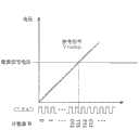
图5A是示出通过切换计数时钟CLKAD的频率来扩大动态范围的图表。FIG. 5A is a graph illustrating expansion of the dynamic range by switching the frequency of the count clock CLKAD.
图5B是示出针对入射光量的AD转换后的值的图表。FIG. 5B is a graph showing AD-converted values for incident light quantities.
图6A是示出计数时钟CLKAD的频率被多次切换的情况下的动态范围的扩大的图表。FIG. 6A is a graph showing expansion of the dynamic range in a case where the frequency of the count clock CLKAD is switched multiple times.
图6B是示出针对入射光量的AD转换后的值的图表。FIG. 6B is a graph showing AD-converted values for incident light quantities.
图7是示出内置有本发明的固体摄像装置的数字相机的大略构成的图。7 is a diagram showing a schematic configuration of a digital camera incorporating the solid-state imaging device of the present invention.
图8A是示出该相机的例子的外观图。FIG. 8A is an external view showing an example of the camera.
图8B是示出内置有本发明的固体摄像装置的摄像机的例子的外观图。8B is an external view showing an example of a video camera incorporating the solid-state imaging device of the present invention.
具体实施方式Detailed ways
以下参照附图对本发明的实施例进行说明。另外,以下说明的实施例仅是一个例子而已,能够进行各种各样的变更。Embodiments of the present invention will be described below with reference to the drawings. In addition, the embodiment described below is just an example, and various changes are possible.
本发明的固体摄像装置,具备:摄像部,具有被配置为矩阵状的多个像素;列信号线,被设置在所述摄像部的每个列;模数转换部,通过对斜坡信号到达来自所述列信号线的像素信号的电压为止的时间进行计数,从而将所述像素信号的电压转换为数字值;以及时钟信号产生部,针对所述模数转换部,产生用于所述计数的时钟信号,所述时钟信号产生部,在模数转换期间,将所述时钟信号的频率从第一频率切换到比第一频率低的第二频率。据此,能够提高像素信号的电压低时的AD转换的分辨率,而降低像素信号的电压高时的AD转换的分辨率,能够扩大动态范围。The solid-state imaging device of the present invention includes: an imaging unit having a plurality of pixels arranged in a matrix; a column signal line provided on each column of the imaging unit; counting the time until the voltage of the pixel signal of the column signal line, thereby converting the voltage of the pixel signal into a digital value; For a clock signal, the clock signal generator switches the frequency of the clock signal from a first frequency to a second frequency lower than the first frequency during analog-to-digital conversion. Accordingly, it is possible to increase the resolution of AD conversion when the voltage of the pixel signal is low, and to decrease the resolution of AD conversion when the voltage of the pixel signal is high, thereby expanding the dynamic range.
图1是示出本发明的实施例所涉及的固体摄像装置的构成的框图。在该图所示的固体摄像装置A是列式MOS图像传感器。具体而言,固体摄像装置A具备传感器核心部B、数字信号处理部8、垂直扫描电路9、定时信号产生器10、参考信号产生部11以及时钟信号产生部C。FIG. 1 is a block diagram showing the configuration of a solid-state imaging device according to an embodiment of the present invention. The solid-state imaging device A shown in the figure is an in-line MOS image sensor. Specifically, the solid-state imaging device A includes a sensor core unit B, a digital signal processing unit 8 , a vertical scanning circuit 9 , a timing signal generator 10 , a reference signal generating unit 11 , and a clock signal generating unit C.
传感器核心部B输出与入射的光的强度对应的数字值。具体而言,传感器核心部B具备像素部1、列放大器2以及列式模数转换器(以下记述为“AD转换部”)3。The sensor core B outputs a digital value corresponding to the intensity of incident light. Specifically, the sensor core unit B includes a
像素部1,具备被配置为矩阵状的单位像素7,基于由垂直扫描电路9输出的信号,按照每个行,将与单位像素7的受光量对应的信号即像素信号,输出到被设置在单位像素7的每个列的列信号线。该像素部1作为摄像部来发挥功能。The
列放大器2对与各个列信号线对应的像素信号进行放大。The column amplifier 2 amplifies pixel signals corresponding to the respective column signal lines.
AD转换部3,通过对由列放大器2放大后的各个像素信号进行数字转换,从而输出与各个像素信号对应的数字值。具体而言,AD转换部3具备:电压比较部4,比较像素信号的电压和参考信号的电压;计数部5,并行于由电压比较部4进行的比较处理来进行计数处理;锁存部6,通过保持由电压比较部4结束了比较处理的时刻的计数值,从而取得像素信号的电压的数字值。电压比较部4,比较像素信号的电压和参考信号产生部11输出的参考信号Vramp的电压,并输出示出参考信号Vramp的电压到达了像素信号的电压的定时的信号。并且,计数部5,基于时钟产生部12输出的计数时钟CLKAD,对从参考信号Vramp产生到参考信号Vramp到达像素信号的电压为止的期间进行计数。锁存部6,保持由电压比较部4输出了示出参考信号Vramp的电压到达像素信号的电压的定时的信号时的、计数部5的计数值。也就是说,锁存部6,保持与像素信号的电压对应的数字值,并将所保持的数字值即数字信号,输出到数字信号处理部8。The AD converter 3 digitally converts each pixel signal amplified by the column amplifier 2 to output a digital value corresponding to each pixel signal. Specifically, the AD conversion unit 3 includes: a voltage comparison unit 4 that compares the voltage of the pixel signal and the voltage of the reference signal; a counting unit 5 that performs counting processing in parallel with the comparison processing performed by the voltage comparison unit 4; and a latch unit 6 The digital value of the voltage of the pixel signal is acquired by holding the count value at the time when the comparison process is completed by the voltage comparison unit 4 . The voltage comparing unit 4 compares the voltage of the pixel signal with the voltage of the reference signal Vramp output from the reference signal generating unit 11, and outputs a signal indicating the timing when the voltage of the reference signal Vramp reaches the voltage of the pixel signal. Then, the counting unit 5 counts a period from when the reference signal Vramp is generated to when the reference signal Vramp reaches the voltage of the pixel signal based on the count clock CLKAD output from the clock generating unit 12 . The latch unit 6 holds the count value of the counter unit 5 when the signal indicating the timing at which the voltage of the reference signal Vramp reaches the voltage of the pixel signal is output from the voltage comparison unit 4 . That is, the latch unit 6 holds a digital value corresponding to the voltage of the pixel signal, and outputs the digital signal, which is the held digital value, to the digital signal processing unit 8 .
数字信号处理部8,对由数字信号处理部8输出的数字信号进行数字增益运算、各种校正处理等,并将处理后的数字信号输出到固体摄像装置A的外部。The digital signal processing unit 8 performs digital gain calculation, various correction processes, etc. on the digital signal output from the digital signal processing unit 8 , and outputs the processed digital signal to the outside of the solid-state imaging device A.
垂直扫描电路9被配置为与像素部1相邻,并将用于控制由各个单位像素7产生的电荷的蓄积时间、用于以行为单位将各个单位像素7的像素信号读出到列信号线的行选择信号,基于定时信号产生器10输出的脉冲信号,按照单位像素7的每个行,将用于控制由各个单位像素7产生的电荷的蓄积时间、用于以行为单位将各个单位像素7的像素信号读出到列信号线的行选择信号,依次输出。垂直扫描电路9,例如是移位寄存器。The vertical scanning circuit 9 is arranged adjacent to the
定时信号产生器10,是控制各个处理部的工作定时的电路,与由外部提供的的主时钟MCLK同步地工作。具体而言,定时信号产生器10,针对垂直扫描电路9控制输出行选择信号的定时,针对参考信号产生部11控制产生参考信号的定时,针对时钟产生部12控制产生计数时钟CLKAD的定时。The timing signal generator 10 is a circuit for controlling the operation timing of each processing unit, and operates in synchronization with an externally supplied master clock MCLK. Specifically, the timing signal generator 10 controls the timing of outputting a row selection signal for the vertical scanning circuit 9 , controls the timing of generating a reference signal for the reference signal generator 11 , and controls the timing of generating the count clock CLKAD for the clock generator 12 .
参考信号产生部11,是与从定时信号产生器10输入的斜坡用时钟CLKDAC联动地工作,并产生AD转换用的参考信号Vramp的电路。具体而言,参考信号Vramp是斜坡波形。The reference signal generation unit 11 is a circuit that operates in conjunction with the ramp clock CLKDAC input from the timing signal generator 10 to generate a reference signal Vramp for AD conversion. Specifically, the reference signal Vramp is a ramp waveform.
时钟信号产生部C,针对AD转换部3产生计数用的时钟信号即计数时钟CLKAD。具体而言,时钟信号产生部C具备时钟产生部12以及时钟控制部13。The clock signal generation unit C generates a count clock CLKAD which is a clock signal for counting to the AD conversion unit 3 . Specifically, the clock signal generation unit C includes a clock generation unit 12 and a clock control unit 13 .
时钟产生部12,基于从时钟控制部13输入的值,与由定时信号产生器10产生的时钟CLKIN同步地产生计数时钟CLKAD。并且,时钟产生部12,将复位信号输出到时钟控制部13。有关时钟产生部12的详细的说明,之后与时钟控制部13的说明一并进行叙述。The clock generation unit 12 generates the count clock CLKAD in synchronization with the clock CLKIN generated by the timing signal generator 10 based on the value input from the clock control unit 13 . Furthermore, the clock generation unit 12 outputs a reset signal to the clock control unit 13 . A detailed description of the clock generation unit 12 will be described later together with a description of the clock control unit 13 .
时钟控制部13,对由时钟产生部12产生的计数时钟CLKAD进行计数,并将该计数值输出到时钟产生部12。并且,由外部,第一频率设定值fAD0、第二频率设定值fAD1以及频率切换值ADCnt0输入到时钟控制部13。具体而言,时钟控制部13具备计数器A14以及计数器B15。计数器A14是与时钟CLKIN的上升以及下降同步地、进行递增1的加计数的计数器。计数器B15是与由时钟产生部12产生的计数时钟CLKAD的上升同步地、直到AD转换部3的AD转换的全范围(full range)进行递增1的加计数的计数器。时钟控制部13将计数器A14以及计数器B15的计数值输出到时钟产生部12。The clock control unit 13 counts the count clock CLKAD generated by the clock generation unit 12 and outputs the count value to the clock generation unit 12 . Furthermore, the first frequency setting value fAD0 , the second frequency setting value fAD1 , and the frequency switching value ADCnt0 are input to the clock control unit 13 from the outside. Specifically, the clock control unit 13 includes a counter A14 and a counter B15. The counter A14 is a counter that counts up by 1 in synchronization with the rising and falling of the clock CLKIN. The counter B15 is a counter that counts up by 1 up to the full range of AD conversion performed by the AD conversion unit 3 in synchronization with the rise of the count clock CLKAD generated by the clock generation unit 12 . The clock control unit 13 outputs the count values of the counter A14 and the counter B15 to the clock generation unit 12 .
其次,对时钟产生部12基于由时钟控制部13输出的计数值而产生计数时钟CLKAD的工作进行说明。Next, the operation of the clock generation unit 12 to generate the count clock CLKAD based on the count value output from the clock control unit 13 will be described.
图2是示出时钟产生部12以及时钟控制部13的工作的时序图。在此,设定AD转换部3的输出位数是12比特(LSB)、第一频率设定值fAD0是1、第二频率设定值fAD1是3、以及频率切换值ADCnt0是1023。该图示出被输入到时钟控制部13的时钟CLKIN、计数器A14的计数值、由时钟产生部12输出的计数时钟CLKAD以及计数器B15的计数值。FIG. 2 is a timing chart showing the operations of the clock generation unit 12 and the clock control unit 13 . Here, the number of output bits of the AD converter 3 is 12 bits (LSB), the first frequency setting value fAD0 is 1, the second frequency setting value fAD1 is 3, and the frequency switching value ADCnt0 is 1023. This figure shows the clock CLKIN input to the clock control unit 13, the count value of the counter A14, the count clock CLKAD output from the clock generation unit 12, and the count value of the counter B15.
首先,计数器14与由定时信号产生器10输出的时钟CLKIN的上升以及下降同步地进行递增1的加计数。时钟产生部12判定计数器A14的计数值是否到达了第一频率设定值fAD0。在计数器A14的计数值未到达第一频率设定值fAD0的情况下,时钟产生部12不使计数时钟CLKAD反相并输出该计数时钟CLKAD。而在计数器A14的计数值到达了第一频率设定值fAD0的情况下,时钟产生部12,在下一个时钟CLKIN的上升或下降,使计数时钟CLKAD的输出反相,并使计数器A14的计数值复位。First, the counter 14 counts up by 1 in synchronization with the rising and falling of the clock CLKIN output from the timing signal generator 10 . The clock generator 12 determines whether or not the count value of the counter A14 has reached the first frequency setting value fAD0. When the count value of the counter A14 has not reached the first frequency setting value fAD0 , the clock generator 12 outputs the count clock CLKAD without inverting the count clock CLKAD. When the count value of the counter A14 reaches the first frequency setting value fAD0, the clock generator 12 inverts the output of the count clock CLKAD when the next clock CLKIN rises or falls, and makes the count value of the counter A14 reset.
也就是说,计数器A14重复进行下述工作,即:直到计数值变为1为止,与被输入到时钟产生部12的CLKIN的上升以及下降同步地一个一个地计数,如果计数值变为1,则复位为0。并且,时钟产生部12,每当计数器A14的计数值到达第一频率设定值fAD0即1时,就使计数时钟CLKAD的输出反相。That is, the counter A14 repeats the operation of counting one by one in synchronization with the rise and fall of CLKIN input to the clock generating part 12 until the count value becomes 1, and when the count value becomes 1, then reset to 0. Furthermore, the clock generation unit 12 inverts the output of the count clock CLKAD every time the count value of the counter A14 reaches 1 which is the first frequency setting value fAD0 .
据此,计数时钟CLKAD成为其周期为时钟CLKIN的周期的2倍的信号。也就是说,时钟产生部12具有这样一种作为分频器的功能,即:以被保持在计数器A14的第一频率设定值fAD0的2倍的分频比来对时钟CLKIN进行分频。Accordingly, the count clock CLKAD becomes a signal whose cycle is twice the cycle of the clock CLKIN. That is, the clock generation section 12 has a function as a frequency divider that divides the frequency of the clock CLKIN at a frequency division ratio of twice the first frequency setting value fAD0 held at the counter A14.
并且,计数器B15与计数时钟CLKAD的上升同步地进行递增1的加计数。时钟产生部12判定计数器B15的计数值是否到达了频率切换值ADCnt0。在计数器B15的计数值未到达频率切换值ADCnt0的情况下,时钟产生部12,按照计数器A14的计数值是否到达了第一频率设定值fAD0,来产生计数时钟CLKAD。Then, the counter B15 counts up by 1 in synchronization with the rise of the count clock CLKAD. The clock generation unit 12 determines whether or not the count value of the counter B15 has reached the frequency switching value ADCnt0. When the count value of the counter B15 has not reached the frequency switching value ADCnt0, the clock generator 12 generates the count clock CLKAD according to whether the count value of the counter A14 has reached the first frequency setting value fAD0.
而在计数器B15的计数值到达了频率切换值ADCnt0即1023的情况下,时钟产生部12,在下一个计数时钟CLKAD的上升时之后,按照计数器A14的计数值是否到达了第二频率设定值fAD1即3,来产生计数时钟CLKAD。以后,同样地,时钟产生部12,在计数器A14的计数值到达了第二频率设定值fAD1即3的情况下,在下一个时钟CLKIN的上升以及下降,使计数时钟CLKAD的输出反相,并且,使计数器A14的计数值复位。And when the count value of the counter B15 reaches the frequency switching value ADCnt0, that is, 1023, the clock generating part 12, after the rising time of the next count clock CLKAD, is determined according to whether the count value of the counter A14 has reached the second frequency setting value fAD1 or not. That is, 3, to generate the count clock CLKAD. Hereafter, similarly, when the count value of the counter A14 reaches the second frequency setting value fAD1, that is, 3, the clock generation unit 12 inverts the output of the count clock CLKAD at the rise and fall of the next clock CLKIN, and , to reset the count value of counter A14.
据此,计数器B15的计数值到达了频率切换值ADCnt0之后的计数时钟CLKAD,成为其周期是时钟CLKIN的周期的6倍的信号。也就是说,成为以第二频率设定值fAD1的2倍的分频比来被分频的信号。Accordingly, the count clock CLKAD after the count value of the counter B15 reaches the frequency switching value ADCnt0 becomes a signal whose cycle is six times the cycle of the clock CLKIN. That is, it becomes a signal frequency-divided by a frequency-division ratio of twice the second frequency setting value fAD1.
这样,时钟产生部12,在计数器B15的计数值超过了频率切换值ADCnt0的时刻,切换计数时钟CLKAD的频率。也就是说,时钟产生部12还具有将作为第一分频比的fAD0×2切换为作为第二分频比的fAD1×2这样一种作为切换部的功能。因此,时钟产生部12,即使不具备用于产生不同的频率的计数时钟CLKAD的多个振荡器,也能将计数时钟CLKAD的频率从第一频率切换为第二频率。In this way, the clock generation unit 12 switches the frequency of the count clock CLKAD at the timing when the count value of the counter B15 exceeds the frequency switching value ADCnt0. That is, the clock generation unit 12 also has a function as a switching unit that switches fAD0×2 as the first frequency division ratio to fAD1×2 as the second frequency division ratio. Therefore, the clock generation unit 12 can switch the frequency of the count clock CLKAD from the first frequency to the second frequency without including a plurality of oscillators for generating the count clock CLKAD of different frequencies.
另外,时钟产生部12,在计数器B15的计数值的12比特都变为1的情况下,在下一个计数时钟CLKAD的上升,使计数器15B的计数值复位。In addition, the clock generating unit 12 resets the count value of the counter 15B at the next rise of the count clock CLKAD when all 12 bits of the count value of the counter B15 become 1.
并且,如该例子所示,计数器A14以及计数器B15,可以与作为基准的时钟的上升或下降同步地进行计数,也可以与作为基准的时钟的上升和下降这双方同步地进行计数。Furthermore, as shown in this example, the counter A14 and the counter B15 may perform counting in synchronization with the rising or falling of the reference clock, or may perform counting in synchronization with both the rising and falling of the reference clock.
其次,说明与被输入到AD转换部3的列信号线对应的像素信号的电压的检测。Next, detection of the voltage of the pixel signal corresponding to the column signal line input to the AD converter 3 will be described.
图3是示出被输入到AD转换部3的计数时钟CLKAD是固定的频率的情况下的、像素信号的电压电平的检测的时序图。该图示出被输入到电压比较部4的像素信号、被输入到电压比较部的参考信号Vramp、以及被输入到计数部5的计数时钟CLKAD的定时。FIG. 3 is a timing chart showing detection of the voltage level of a pixel signal when the count clock CLKAD input to the AD converter 3 has a fixed frequency. This figure shows the timing of the pixel signal input to the voltage comparison section 4 , the reference signal Vramp input to the voltage comparison section, and the count clock CLKAD input to the count section 5 .
电压比较部4,依次比较以斜坡状变化的参考信号Vramp的电压与像素信号的电压。并且,计数部5基于计数时钟CLKAD来进行计数工作。锁存部6,保持在参考信号Vramp的电压与像素信号的电压一致时由计数部5计数的计数值,并将所保持的计数值作为数字数据输出到数字信号处理部8。The voltage comparison unit 4 sequentially compares the voltage of the reference signal Vramp that changes in a ramp shape with the voltage of the pixel signal. And, the counting unit 5 performs a counting operation based on the count clock CLKAD. The latch unit 6 holds the count value counted by the count unit 5 when the voltage of the reference signal Vramp matches the voltage of the pixel signal, and outputs the held count value to the digital signal processing unit 8 as digital data.
这样,AD转换部3,比较参考信号Vramp的电压与像素信号的电压,并将在参考信号Vramp的电压到达了像素信号的电压时的计数部5的计数值,作为与像素信号的电压对应的数字数据来提取,从而进行AD转换。In this way, the AD conversion unit 3 compares the voltage of the reference signal Vramp with the voltage of the pixel signal, and uses the count value of the counting unit 5 when the voltage of the reference signal Vramp reaches the voltage of the pixel signal as a value corresponding to the voltage of the pixel signal. Digital data is extracted for AD conversion.
其次,说明被输入到AD转换部3的计数时钟CLKAD的频率在AD转换的期间被切换的情况下的、像素信号的电压的检测。Next, detection of the voltage of the pixel signal when the frequency of the count clock CLKAD input to the AD conversion unit 3 is switched during AD conversion will be described.
图4是示出被输入到AD转换部3的计数时钟CLKAD的频率被切换的情况下的、图像信号的电压电平的检测的时序图。与图3比较,该图中在频率切换时的前后,计数时钟CLKAD的频率不同。例如,在频率切换值ADCnt0是1023的情况下,在计数器B15的计数值到达了1023后的下一个计数时钟CLKAD的上升开始,计数时钟CLKAD的频率变低。FIG. 4 is a timing chart showing the detection of the voltage level of the image signal when the frequency of the count clock CLKAD input to the AD converter 3 is switched. Compared with FIG. 3 , in this figure, the frequency of the count clock CLKAD is different before and after the frequency switching. For example, when the frequency switching value ADCnt0 is 1023, the count clock CLKAD starts to rise next after the count value of the counter B15 reaches 1023, and the frequency of the count clock CLKAD becomes low.
参考信号Vramp是其电压相对于时刻以一定的比例增加的波形,因此时间变化越小,对应的电压变化也越小。并且,计数器A14的最大计数值是第一频率设定值fAD0的期间,与计数器A14的最大计数值是第二频率设定值fAD1的期间相比,计数时钟CLKAD的周期短。因此,对计数器B15的计数值超过频率切换值ADCnt0为止的期间的电压的分辨率,与超过之后的电压的分辨率进行比较,则可知超过频率切换值ADCnt0为止的分辨率高于超过之后的分辨率。The reference signal Vramp is a waveform whose voltage increases at a certain ratio relative to time, so the smaller the time variation is, the smaller the corresponding voltage variation is. Furthermore, the period during which the maximum count value of the counter A14 is the first frequency setting value fAD0 is shorter than the period during which the maximum count value of the counter A14 is the second frequency setting value fAD1. Therefore, comparing the resolution of the voltage during the period until the count value of the counter B15 exceeds the frequency switching value ADCnt0 with the resolution of the voltage after exceeding, it can be seen that the resolution until the count value of the counter B15 exceeds the frequency switching value ADCnt0 is higher than the resolution after exceeding. Rate.
这样,本发明的固体摄像装置A,通过变更被输入到计数部5的计数时钟CLKAD的频率,能够使像素信号的分辨率不同来进行AD转换。计数时钟CLKAD的频率越高,能够越细致地对变换对象的电压范围内的信号进行AD转换,能够提高分辨率来进行AD转换。Thus, in the solid-state imaging device A of the present invention, by changing the frequency of the count clock CLKAD input to the count unit 5 , it is possible to perform AD conversion with different resolutions of pixel signals. The higher the frequency of the count clock CLKAD, the finer the AD conversion can be performed on the signal in the voltage range to be converted, and the AD conversion can be performed with higher resolution.
其次,说明本发明的固体摄像装置A的动态范围的扩大。具体而言,说明通过变更被输入到AD转换部3的计数时钟CLKAD的频率来扩大动态范围。Next, expansion of the dynamic range of the solid-state imaging device A of the present invention will be described. Specifically, expansion of the dynamic range by changing the frequency of the count clock CLKAD input to the AD conversion unit 3 will be described.
图5A是示出在计数时钟CLKAD的频率单一的情况下和在中途变更的情况下的、可进行AD转换的电压范围的图表。在该图中,单一频率的情况下的计数时钟CLKAD的频率,与切换频率的情况下的切换前的频率,即由第一频率设定值fAD0来决定的频率相同。FIG. 5A is a graph showing a voltage range in which AD conversion can be performed when the frequency of the count clock CLKAD is single and when it is changed midway. In the figure, the frequency of the count clock CLKAD in the case of the single frequency is the same as the frequency before switching in the case of the switching frequency, that is, the frequency determined by the first frequency setting value fAD0.
图5A的横轴示出计数时钟CLKAD是单一频率的情况下以及中途切换的情况下的、计数时钟CLKAD的定时和对应的计数器B15的计数值。ADCfull是计数器B15饱和时的计数值。例如,在计数器B15是12比特的计数器的情况下,ADCfull是4095。The horizontal axis of FIG. 5A shows the timing of the count clock CLKAD and the corresponding count value of the counter B15 when the count clock CLKAD has a single frequency and when it is switched midway. ADCfull is the count value when counter B15 is saturated. For example, when the counter B15 is a 12-bit counter, ADCfull is 4095.
并且,纵轴示出与计数值对应的参考信号Vramp的电压。在此,在计数时钟CLKAD是单一频率的情况下,Vr1是计数器B15的计数值变为ADCfull时的电压。并且,在计数时钟CLKAD在中途被切换的情况下,Vr2是计数器B15的计数值变为ADCfull时的电压。Also, the vertical axis shows the voltage of the reference signal Vramp corresponding to the count value. Here, when the count clock CLKAD has a single frequency, Vr1 is a voltage at which the count value of the counter B15 becomes ADCfull. Furthermore, when the count clock CLKAD is switched midway, Vr2 is a voltage at which the count value of the counter B15 becomes ADCfull.
如该图所示,与计数时钟CLKAD是单一的频率的情况下的饱和电平电压Vr1相比,在中途将频率切换为低频率的情况下的饱和电平电压Vr高。这是因为,通过在中途将频率切换为低频率,切换以后的计数所需要的期间延长,与该延长时间对应的参考信号Vramp相应地能够进行AD转换的电压增加。As shown in the figure, the saturation level voltage Vr when the frequency is switched to a low frequency on the way is higher than the saturation level voltage Vr1 when the count clock CLKAD has a single frequency. This is because, by switching the frequency to a low frequency on the way, the period required for counting after switching is extended, and the reference signal Vramp corresponding to this extended time increases the voltage at which AD conversion can be performed.
图5B是示出切换计数时钟CLKAD的频率的情况下的、针对入射光量的AD转换后的值的图表。该图的横轴示出入射到单位像素7的光量即入射光量,纵轴示出计数器B15的计数值。FIG. 5B is a graph showing AD-converted values for incident light quantities when the frequency of the count clock CLKAD is switched. In this figure, the horizontal axis shows the amount of light incident on the unit pixel 7 , that is, the incident light amount, and the vertical axis shows the count value of the counter B15 .
计数时钟CLKAD是单一的频率的情况下,AD转换部3的分辨率总是固定的。与此相对,在切换计数时钟CLKAD的频率的情况下,在计数时钟CLKAD的频率的切换前后,AD转换部3的分辨率不同。When the count clock CLKAD has a single frequency, the resolution of the AD converter 3 is always constant. On the other hand, when the frequency of the count clock CLKAD is switched, the resolution of the AD converter 3 is different before and after switching the frequency of the count clock CLKAD.
这是因为,例如在第二频率设定值fAD1是意味着2倍于第一频率设定值fAD0的值(例如,fAD0是1、fAD1是3)的情况下,基于fAD1而产生的计数时钟CLKAD的周期是基于fAD0而产生的计数时钟CLKAD的周期的2倍。因此,计数器B 15的计数值超过频率切换值ADCnt0,时钟产生部12切换了计数时钟CLKAD的频率后的AD转换的分辨率,与切换前的分辨率相比,是切换前的分辨率的1/2。也就是说,切换后,针对入射光量的输出信号的增益是1/2。This is because, for example, when the second frequency setting value fAD1 is a value twice the first frequency setting value fAD0 (for example, fAD0 is 1 and fAD1 is 3), the count clock generated based on fAD1 The cycle of CLKAD is twice the cycle of the count clock CLKAD generated based on fAD0. Therefore, the count value of the counter B 15 exceeds the frequency switching value ADCnt0, and the resolution of the AD conversion after the frequency of the count clock CLKAD is switched by the clock generation unit 12 is 1 of the resolution before switching compared with the resolution before switching. /2. That is, after switching, the gain of the output signal with respect to the amount of incident light is 1/2.
据此,在中途切换计数时钟CLKAD的频率来进行AD转换的情况下的动态范围,与以固定的计数时钟CLKAD进行了AD转换的情况相比,动态范围能够从DR0扩大到DR1。该动态范围的差分(DR1-DR0)是这样的值,即:将与以固定的计数时钟CLKAD进行了AD转换的情况下的AD转换的全范围(full range)对应的入射光量,和与切换了频率的时刻的AD转换的输出信号对应的入射光量之间的差分,除以切换前的分辨率与切换后的分辨率的比例,而得到的值。Accordingly, the dynamic range when AD conversion is performed by switching the frequency of count clock CLKAD halfway can be expanded from DR0 to DR1 compared to the case where AD conversion is performed with a fixed count clock CLKAD. The difference (DR1-DR0) of this dynamic range is such a value that the incident light amount corresponding to the full range (full range) of AD conversion in the case where AD conversion is performed with a fixed count clock CLKAD, and the switching The value obtained by dividing the difference between the incident light quantities corresponding to the AD converted output signal at the time when the frequency is changed by the ratio of the resolution before switching to the resolution after switching.
例如,计数器B15是12比特(0~4095)的计数器、ADCnt0是1023、fAD0是1、fAD1是3的情况下,与不切换频率而以与fAD0是1的情况下的计数时钟CLKAD的频率相同的频率进行AD转换的情况相比,动态范围是7/4倍。For example, when the counter B15 is a 12-bit (0 to 4095) counter, ADCnt0 is 1023, fAD0 is 1, and fAD1 is 3, the frequency of the count clock CLKAD is the same as when fAD0 is 1 without switching the frequency. The dynamic range is 7/4 times that of the case where the AD conversion is performed at the frequency.
这样,通过将频率切换值ADCnt0的值设定为计数器B15的范围内的任意的值,从而能够任意地变更时钟产生部12切换计数时钟CLKAD的频率的定时。并且,能够基于该频率切换值ADCnt0的值而变更动态范围的扩大程度。具体而言,频率切换值ADCnt0的值越小,越能扩大动态范围。In this way, by setting the value of the frequency switching value ADCnt0 to an arbitrary value within the range of the counter B15, the timing at which the clock generation unit 12 switches the frequency of the count clock CLKAD can be arbitrarily changed. Furthermore, the degree of expansion of the dynamic range can be changed based on the value of the frequency switching value ADCnt0. Specifically, the smaller the frequency switching value ADCnt0 is, the more the dynamic range can be expanded.
如以上所述,本发明的固体摄像装置A,能够在计数时钟CLKAD的频率的切换前后变更AD转换的分辨率。因此,能够提高像素信号的电压低时的分辨率,而降低像素信号的电压高时的分辨率,以扩大动态范围,处理更强的入射光。As described above, the solid-state imaging device A of the present invention can change the AD conversion resolution before and after switching the frequency of the count clock CLKAD. Therefore, it is possible to increase the resolution when the voltage of the pixel signal is low, and reduce the resolution when the voltage of the pixel signal is high, so as to expand the dynamic range and process stronger incident light.
另外,时钟产生部12,可以多次切换计数时钟CLKAD的频率。其次,说明被输入到AD转换部3的计数时钟CLKAD的频率被多次切换的情况下的动态范围的扩大。In addition, the clock generation unit 12 may switch the frequency of the count clock CLKAD multiple times. Next, expansion of the dynamic range when the frequency of the count clock CLKAD input to the AD conversion unit 3 is switched multiple times will be described.
图6A是示出多次切换计数时钟CLKAD的频率的情况下的、可进行AD转换的电压范围的图表。FIG. 6A is a graph showing a voltage range in which AD conversion is possible when the frequency of the count clock CLKAD is switched multiple times.
例如,如图6A所示的第一频率设定值fAD2、第二频率设定值fAD3以及第三频率设定值fAD4,和第一频率切换值ADCnt1以及第二频率切换值ADCnt2这样来设定多个频率设定值和频率切换值。For example, the first frequency setting value fAD2, the second frequency setting value fAD3, and the third frequency setting value fAD4 shown in FIG. 6A, and the first frequency switching value ADCnt1 and the second frequency switching value ADCnt2 are set in this way Multiple frequency setpoints and frequency switching values.
图6B是示出多次切换计数时钟CLKAD的频率的情况下的、针对入射光量的AD转换后的值的图表。FIG. 6B is a graph showing AD-converted values for incident light quantities in the case where the frequency of the count clock CLKAD is switched multiple times.
此时,如该图所示,分辨率多次变化。At this time, as shown in the figure, the resolution is changed multiple times.
在多次切换计数时钟CLKAD的频率的情况下,与计数时钟CLKAD的上升同步进行计数的计数器B15的计数值到达第一频率切换值ADCnt1为止,与时钟CLKIN的上升以及下降同步进行计数的计数器A14,重复进行到达fAD2为止的计数,时钟产生部12产生与fAD2对应的周期的计数时钟CLKAD。同样地依次进行以下的工作,即:计数器B15到达第二频率切换值ADCnt2为止,计数器A14重复到第二频率设定值fAD3为止的计数,时钟产生部12产生与fAD3对应的周期的计数时钟CLKAD。When the frequency of the count clock CLKAD is switched multiple times, the counter A14 that counts in synchronization with the rise and fall of the clock CLKIN until the count value of the counter B15 that counts in synchronization with the rise of the count clock CLKAD reaches the first frequency switching value ADCnt1 , counting up to fAD2 is repeated, and the clock generator 12 generates a count clock CLKAD of a period corresponding to fAD2. Similarly, the following operations are performed sequentially, that is, until the counter B15 reaches the second frequency switching value ADCnt2, the counter A14 repeats the counting up to the second frequency setting value fAD3, and the clock generation part 12 generates the count clock CLKAD of the period corresponding to fAD3 .
在此,设定为fAD4>fAD3>fAD2,则如图6B所示,与低照度侧相比能使高照度侧的AD转换分辨率更粗糙。据此,与以固定的计数时钟CLKAD进行AD转换的情况相比,中途多次切换计数时钟CLKAD的频率的情况下的动态范围能够从DR2扩大到DR3。Here, if fAD4>fAD3>fAD2 is set, as shown in FIG. 6B , the AD conversion resolution can be made coarser on the high-illuminance side than on the low-illuminance side. According to this, compared with the case of performing AD conversion with a fixed count clock CLKAD, the dynamic range can be expanded from DR2 to DR3 when the frequency of the count clock CLKAD is switched multiple times on the way.
并且,能够进一步设定多个频率设定值以及频率切换值,通过依次增大设定值来使高照度侧的AD转换分辨率比低照度侧的AD转换分辨率更粗糙,从而更加扩大动态范围。In addition, multiple frequency setting values and frequency switching values can be further set, and by increasing the setting values sequentially, the AD conversion resolution on the high-illuminance side is coarser than that on the low-illuminance side, thereby further expanding the dynamic range. scope.
一般地,数字相机等摄像装置的信号处理中,进行伽马校正、拐点(knee)校正这样的处理,并针对所取得的图像信号,进行对信号电平为低中照度的信号进行放大处理而对信号电平为高照度的信号进行压缩处理这样的处理。在进行这样的处理的情况下,通过提高信号电平是低中照度的信号的分辨率,从而能够改善在后级的信号处理中被放大的区域的信号成分的S/N,能够提高画质。Generally, in the signal processing of an imaging device such as a digital camera, processing such as gamma correction and knee correction is performed, and a signal with a signal level of a low-medium illuminance is amplified for the obtained image signal. A process of performing compression processing on a signal whose signal level is high illuminance. When such processing is performed, the S/N of the signal components in the area to be amplified in the subsequent signal processing can be improved by improving the resolution of the signal whose signal level is low-medium illuminance, and the image quality can be improved. .
并且,时钟控制部13,在中途切换计数时钟CLKAD的频率的情况下,按照切换前后的频率来变更参考信号Vramp的期间。具体而言,时钟产生部12,将示出在输出的计数时钟CLKAD的频率的信息,输出到时钟控制部13。时钟控制部13,基于由时钟产生部12输出的示出计数时钟CLKAD的频率的信息,使参考信号Vramp能够被输出直到计数器B15的计数值饱和的定时为止。Furthermore, when the frequency of the count clock CLKAD is switched midway, the clock control unit 13 changes the period of the reference signal Vramp according to the frequency before and after the switching. Specifically, the clock generation unit 12 outputs information indicating the frequency of the output count clock CLKAD to the clock control unit 13 . The clock control unit 13 enables the reference signal Vramp to be output until the count value of the counter B15 is saturated based on the information indicating the frequency of the count clock CLKAD output by the clock generation unit 12 .
另外,虽然在上述实施例的图5A以及图5B中,对计数时钟CLKAD的频率固定的情况下的频率和与第一频率设定值fAD0对应的计数时钟CLKAD的频率相同的情况下的动态范围的扩大进行了说明,但是也可以是,与第一频率设定值fAD0对应的计数时钟CLKAD的频率比计数时钟CLKAD的频率固定的情况下的频率高。此时,与计数时钟CLKAD的频率固定的情况下的分辨率相比,能够更加提高低照度侧的分辨率。In addition, although in FIG. 5A and FIG. 5B of the above-mentioned embodiment, the dynamic range when the frequency of the count clock CLKAD is fixed and the frequency of the count clock CLKAD corresponding to the first frequency setting value fAD0 is the same However, the frequency of the count clock CLKAD corresponding to the first frequency setting value fAD0 may be higher than the frequency when the frequency of the count clock CLKAD is fixed. In this case, the resolution on the low-illuminance side can be further improved compared to the resolution when the frequency of the count clock CLKAD is fixed.
据此,与计数时钟CLKAD的频率固定的情况下的动态范围相比,能够将动态范围向低照度侧扩大。This makes it possible to expand the dynamic range toward the low-illuminance side compared to the dynamic range when the frequency of the count clock CLKAD is constant.
并且,本发明的固体摄像装置A中,AD转换的期间包括第一期间和第二期间,时钟产生部12在第一期间产生第一频率的计数时钟CLKAD,在第二期间产生比第一频率低的第二频率的计数时钟CLKAD,并且也可以是,第一期间在第二期间以下。In addition, in the solid-state imaging device A of the present invention, the period of AD conversion includes a first period and a second period, and the clock generator 12 generates a count clock CLKAD of a first frequency during the first period, and generates a count clock CLKAD of a frequency higher than the first frequency during the second period. The count clock CLKAD of the second frequency is low, and the first period may be less than the second period.
据此,通过重点地提高像素信号的电压低时的分辨率,从而能够放大低照度侧的信号成分,能够提高低照度侧的S/N。并且,通过降低像素信号的电压高时的分辨率,从而能够使AD转换的输入范围照样宽广。Accordingly, by focusing on improving the resolution when the voltage of the pixel signal is low, it is possible to amplify the signal component on the low-illuminance side and improve the S/N on the low-illuminance side. Furthermore, by lowering the resolution when the voltage of the pixel signal is high, the input range of the AD conversion can be widened as it is.
并且,虽然在本发明的固体摄像装置A中AD转换部3具备计数部5,但是也可以是,AD转换部3不具备计数部5。此时,锁存部6保持由电压比较部4输出下述信号时的计数器B15的计数值,该信号是示出参考信号Vramp的电压到达了像素信号的电压的定时的信号。据此,能够简化AD转换部3的构成,能够使固体摄像装置的大小变小。Furthermore, although the AD conversion unit 3 includes the counting unit 5 in the solid-state imaging device A of the present invention, the AD conversion unit 3 may not include the counting unit 5 . At this time, the latch unit 6 holds the count value of the counter B15 when the voltage comparison unit 4 outputs a signal indicating the timing at which the voltage of the reference signal Vramp reaches the voltage of the pixel signal. Accordingly, the configuration of the AD converter 3 can be simplified, and the size of the solid-state imaging device can be reduced.
并且,在上述实施例中,虽然时钟产生部12,在像素信号的低照度侧提高计数时钟CLKAD的频率,在像素信号的高照度侧降低计数时钟CLKAD的频率,但是计数时钟CLKAD的频率也可以不限定于此。例如,也可以是,像素信号的高照度侧高而像素信号的低照度侧低。并且,也可以是,例如,在像素信号的任意的照度范围内,提高计数时钟CLKAD的频率。In addition, in the above-mentioned embodiment, although the clock generation unit 12 increases the frequency of the count clock CLKAD on the low-illuminance side of the pixel signal, and decreases the frequency of the count clock CLKAD on the high-illuminance side of the pixel signal, the frequency of the count clock CLKAD may be Not limited to this. For example, the high illuminance side of the pixel signal may be high and the low illuminance side of the pixel signal may be low. Furthermore, for example, the frequency of the count clock CLKAD may be increased in an arbitrary illuminance range of the pixel signal.
据此,在像素信号的任意的照度范围内,能够更加放大信号成分,能够提高S/N。并且,在任意的照度范围之外,通过降低计数时钟CLKAD的频率来降低分辨率,从而能够使动态范围照样宽广。Accordingly, in an arbitrary illuminance range of the pixel signal, the signal component can be further amplified, and the S/N can be improved. In addition, outside any illuminance range, by reducing the frequency of the count clock CLKAD to reduce the resolution, the dynamic range can be widened as it is.
并且,本发明不仅能够作为固体摄像装置来实现,而且也能够作为控制固体摄像装置的AD转换方法来实现。Furthermore, the present invention can be realized not only as a solid-state imaging device but also as an AD conversion method for controlling the solid-state imaging device.
(数字相机的构成)(Construction of digital camera)
并且,不言而喻,内置有本发明的固体摄像装置A的各种电子设备也包含在本发明中。图7是示出利用了上述的固体摄像装置A的数字相机的大略构成的图。In addition, it goes without saying that various electronic devices incorporating the solid-state imaging device A of the present invention are also included in the present invention. FIG. 7 is a diagram showing a schematic configuration of a digital camera using the solid-state imaging device A described above.
如图7所示,数字相机D具备:使被摄物的光学像成像于摄像元件上的透镜16;对通过透镜后的光学像进行光学处理的光圈、反射镜以及快门等的光学系统17;MOS型的固体摄像装置A;进行固体摄像装置A的驱动控制、由固体摄像装置A取得的图像信号的处理的DSP18;在监视器等显示装置映出所取得的图像的显示部19;以及在规定的记录介质记录图像的记录部20等。As shown in FIG. 7 , the digital camera D is provided with: a
来自被摄物的光学像通过透镜16以及光学系统17内的光圈来被调整为恰当的明亮度,并入射到固体摄像装置A。此时,透镜16将焦点位置调整为使来自被摄物的光学像成像于固体摄像装置A所包括的像素部1上。通过串行接口等通信单元来进行由DSP18向固体摄像装置A的驱动控制,并且,对固体摄像装置A内的时钟控制部13的频率设定值的设定、对频率切换值的设定也利用该通信单元来进行。DSP18中,针对从固体摄像装置A取得的图像信号,进行伽马校正、拐点校正、白平衡(White Balance)、减噪等各种校正处理、YC处理、图像压缩处理等,并将图像信号输出到显示部19、记录部20。The optical image from the subject is adjusted to an appropriate brightness by the
根据这样的数字相机D,能够通过本发明的固体摄像装置A来扩大动态范围,能够改善低照度侧的S/N,能够提高画质。并且,因为能够抑制固体摄像装置A的芯片面积的增大,因而能够实现小型的数字相机,例如,作为图8A所示的数字静相相机、图8B所示的摄像机来实现。另外,图8A以及图8B中能够适当地组合固体摄像装置A、DSP18以及记录部20,来进行单芯片化。According to such a digital camera D, the dynamic range can be expanded by the solid-state imaging device A of the present invention, the S/N on the low-illuminance side can be improved, and the image quality can be improved. In addition, since the increase in the chip area of the solid-state imaging device A can be suppressed, a compact digital camera can be realized, for example, as a digital still camera shown in FIG. 8A or a video camera shown in FIG. 8B . In addition, in FIGS. 8A and 8B , the solid-state imaging device A, the
以上,基于本发明的实施例进行了说明,但是本发明并不限定于这些实施例。只要不超出本发明的宗旨,对这些实施例施加了本领域的同行业人员所能想到的各种变形后的实施例,也包含在本发明的范围内。As mentioned above, although the Example of this invention was demonstrated based on it, this invention is not limited to these Examples. As long as it does not deviate from the gist of the present invention, embodiments in which various modifications conceivable by those skilled in the art are added to these embodiments are also included in the scope of the present invention.
工业实用性Industrial Applicability
本发明所涉及的固体摄像装置,能够以简易的构成来实现即使在大光量的光入射的情况下也能够不易产生饱和的高动态范围的固体摄像装置,例如,能够被利用于最适于在屋内与屋外间的光量变化大的拍摄条件下的数字相机,除此之外还能够被利用于附带相机的移动电话、监视相机等各种各样的利用了固体摄像装置的相机系统。The solid-state imaging device according to the present invention can realize a solid-state imaging device with a high dynamic range in which saturation is less likely to occur even when a large amount of light is incident with a simple configuration. Digital cameras under shooting conditions where the amount of light varies greatly between indoors and outdoors can be used in various camera systems using solid-state imaging devices, such as mobile phones with cameras and surveillance cameras.
符号说明Symbol Description
A 固体撮像装置A Solid-state imaging device
B 传感器核心部B Sensor Core
C 时钟信号产生部C Clock signal generator
D 数字相机D digital camera
1 像素部1 pixel unit
2 列放大器2 column amplifiers
3 AD转换部3 AD conversion department
4 电压比较部4 Voltage comparison part
5 计数部5 counting department
6 锁存部6 latch unit
7 单位像素7 unit pixel
8 数字信号处理部8 Digital Signal Processing Department
9 垂直扫描电路9 vertical scanning circuit
10 定时信号产生器10 timing signal generator
11 参考信号产生部11 Reference signal generator
12 时钟产生部12 Clock generation part
13 时钟控制部13 Clock Control Department
14 计数器A14 Counter A
15 计数器B15 Counter B
16 透镜16 lenses
17 光学系统17 Optical system
18 DSP18 DSPs
19 显示部19 Display
20 记录部20 Department of Records
Claims (8)
Applications Claiming Priority (3)
| Application Number | Priority Date | Filing Date | Title |
|---|---|---|---|
| JP2008331626AJP2010154372A (en) | 2008-12-25 | 2008-12-25 | Solid-state imaging device, digital camera, and ad conversion method |
| JP2008-331626 | 2008-12-25 | ||
| PCT/JP2009/007058WO2010073584A1 (en) | 2008-12-25 | 2009-12-21 | Solid-state image pickup device, digital camera, and a/d conversion method |
Publications (1)
| Publication Number | Publication Date |
|---|---|
| CN102265606Atrue CN102265606A (en) | 2011-11-30 |
Family
ID=42287233
Family Applications (1)
| Application Number | Title | Priority Date | Filing Date |
|---|---|---|---|
| CN2009801523193APendingCN102265606A (en) | 2008-12-25 | 2009-12-21 | Solid-state imaging device, digital camera, and AD conversion method |
Country Status (4)
| Country | Link |
|---|---|
| US (1) | US20110248145A1 (en) |
| JP (1) | JP2010154372A (en) |
| CN (1) | CN102265606A (en) |
| WO (1) | WO2010073584A1 (en) |
Cited By (5)
| Publication number | Priority date | Publication date | Assignee | Title |
|---|---|---|---|---|
| CN103369261A (en)* | 2013-06-25 | 2013-10-23 | 天津大学 | Method and device for improving linear dynamic range of PWM (Pulse Width Modulation) pixel |
| CN104580951A (en)* | 2013-10-18 | 2015-04-29 | 瑞萨电子株式会社 | Solid-state image sensing device |
| CN106165401A (en)* | 2014-04-16 | 2016-11-23 | 索尼公司 | Imaging element, gain control method, program and electronic device |
| CN111936882A (en)* | 2018-03-28 | 2020-11-13 | 松下知识产权经营株式会社 | Solid-state imaging device, solid-state imaging system, and driving method of solid-state imaging device |
| CN115209076A (en)* | 2021-04-14 | 2022-10-18 | 三星电子株式会社 | Image forming apparatus and method of operating the same |
Families Citing this family (13)
| Publication number | Priority date | Publication date | Assignee | Title |
|---|---|---|---|---|
| JP2012191359A (en)* | 2011-03-09 | 2012-10-04 | Sony Corp | A/d conversion device, a/d conversion method and program |
| JPWO2012143982A1 (en)* | 2011-04-21 | 2014-07-28 | パナソニック株式会社 | Ramp generation circuit, and image sensor and imaging apparatus including the same |
| JP5901212B2 (en)* | 2011-10-07 | 2016-04-06 | キヤノン株式会社 | Photoelectric conversion system |
| KR102210539B1 (en) | 2013-12-26 | 2021-02-01 | 삼성전자주식회사 | correlated double sampling circuit, analog-to digital converter and image sensor including the same |
| KR102326607B1 (en)* | 2014-07-14 | 2021-11-16 | 소니그룹주식회사 | Comparator, ad converter, solid-state image pickup device, electronic apparatus, and method for controlling comparator |
| KR102261595B1 (en)* | 2014-09-19 | 2021-06-04 | 삼성전자주식회사 | An image sensor, and an image processing system including the same |
| TWI684363B (en)* | 2015-02-13 | 2020-02-01 | 日商新力股份有限公司 | Image sensor, readout control method, and electronic device |
| JP6295985B2 (en)* | 2015-03-13 | 2018-03-20 | 株式会社豊田中央研究所 | Time measuring circuit and temperature sensor circuit having the same |
| KR20170003744A (en)* | 2015-06-30 | 2017-01-10 | 에스케이하이닉스 주식회사 | Image sensing device |
| JP2017046259A (en)* | 2015-08-28 | 2017-03-02 | ルネサスエレクトロニクス株式会社 | Semiconductor device |
| KR102520467B1 (en)* | 2016-09-23 | 2023-04-12 | 에스케이하이닉스 주식회사 | Count circuit, method of driving the count circuit, and image sensing device with the count circuit |
| EP3606043B1 (en)* | 2018-03-30 | 2023-08-16 | Shenzhen Goodix Technology Co., Ltd. | Analog-to-digital converter circuit, image sensor, and analog-to-digital conversion method |
| WO2024195290A1 (en)* | 2023-03-22 | 2024-09-26 | ソニーセミコンダクタソリューションズ株式会社 | Solid-state imaging element, imaging device, and method for controlling solid-state imaging element |
Family Cites Families (25)
| Publication number | Priority date | Publication date | Assignee | Title |
|---|---|---|---|---|
| US4860374A (en)* | 1984-04-19 | 1989-08-22 | Nikon Corporation | Apparatus for detecting position of reference pattern |
| JP4560205B2 (en)* | 2000-12-18 | 2010-10-13 | キヤノン株式会社 | A / D converter and solid-state imaging device using the same |
| US8169517B2 (en)* | 2001-03-26 | 2012-05-01 | Panavision Imaging Llc | Image sensor ADC and CDS per column with oversampling |
| JP4107269B2 (en)* | 2004-02-23 | 2008-06-25 | ソニー株式会社 | Solid-state imaging device |
| JP2006020172A (en)* | 2004-07-02 | 2006-01-19 | Fujitsu Ltd | Ramp waveform generation circuit, analog / digital conversion circuit, imaging device, and imaging device control method |
| JP4289244B2 (en)* | 2004-07-16 | 2009-07-01 | ソニー株式会社 | Image processing method, semiconductor device for detecting physical quantity distribution, and electronic apparatus |
| JP4654857B2 (en)* | 2005-09-26 | 2011-03-23 | ソニー株式会社 | DA converter, AD converter, semiconductor device |
| US8179296B2 (en)* | 2005-09-30 | 2012-05-15 | The Massachusetts Institute Of Technology | Digital readout method and apparatus |
| KR100830582B1 (en)* | 2006-11-13 | 2008-05-22 | 삼성전자주식회사 | Digital double sampling method and CMOS image sensor performing it and digital camera including it |
| US7839439B2 (en)* | 2007-01-12 | 2010-11-23 | Sony Corporation | Solid-state imaging device and imaging device |
| US8237808B2 (en)* | 2007-01-17 | 2012-08-07 | Sony Corporation | Solid state imaging device and imaging apparatus adjusting the spatial positions of pixels after addition by controlling the ratio of weight values during addition |
| KR100871828B1 (en)* | 2007-01-29 | 2008-12-03 | 삼성전자주식회사 | CMOS image sensor comprising a single slope ADC using hysteresis characteristics and a conversion method thereof, and the single slope ADC |
| JP5076568B2 (en)* | 2007-03-12 | 2012-11-21 | ソニー株式会社 | DATA PROCESSING METHOD, DATA PROCESSING DEVICE, SOLID-STATE IMAGING DEVICE, IMAGING DEVICE, ELECTRONIC DEVICE |
| US7656338B2 (en)* | 2007-05-23 | 2010-02-02 | Seiko Epson Corporation | Analog-digital converter and image sensor |
| JP4389981B2 (en)* | 2007-08-06 | 2009-12-24 | ソニー株式会社 | Solid-state imaging device, analog-digital conversion method of solid-state imaging device, and imaging device |
| JP4403435B2 (en)* | 2007-11-16 | 2010-01-27 | ソニー株式会社 | Solid-state imaging device, drive control method, and imaging device |
| JP2009159331A (en)* | 2007-12-26 | 2009-07-16 | Panasonic Corp | Solid-state imaging device, driving method thereof and camera |
| KR20090069803A (en)* | 2007-12-26 | 2009-07-01 | 삼성전자주식회사 | Lamp signal generator and image sensor including the same |
| JP4442695B2 (en)* | 2008-02-29 | 2010-03-31 | ソニー株式会社 | Solid-state imaging device and camera device |
| KR101565967B1 (en)* | 2008-04-21 | 2015-11-06 | 삼성전자주식회사 | Sigma-delta analog-to-digital conversion method and apparatus |
| JP4618349B2 (en)* | 2008-08-11 | 2011-01-26 | ソニー株式会社 | Solid-state imaging device, imaging method, and imaging apparatus |
| JP5165520B2 (en)* | 2008-10-01 | 2013-03-21 | ソニー株式会社 | Solid-state imaging device, imaging device, and AD conversion method for solid-state imaging device |
| JP5365223B2 (en)* | 2009-01-29 | 2013-12-11 | 富士通セミコンダクター株式会社 | Imaging apparatus, signal processing method for imaging apparatus, and image sensor chip |
| US8586903B2 (en)* | 2009-11-23 | 2013-11-19 | Samsung Electronics Co., Ltd. | Counter circuits, analog to digital converters, image sensors and digital imaging systems including the same |
| KR101118576B1 (en)* | 2010-11-10 | 2012-02-27 | 주식회사 하이닉스반도체 | Analog to digital converter |
- 2008
- 2008-12-25JPJP2008331626Apatent/JP2010154372A/enactivePending
- 2009
- 2009-12-21WOPCT/JP2009/007058patent/WO2010073584A1/enactiveApplication Filing
- 2009-12-21CNCN2009801523193Apatent/CN102265606A/enactivePending
- 2011
- 2011-06-16USUS13/161,768patent/US20110248145A1/ennot_activeAbandoned
Cited By (6)
| Publication number | Priority date | Publication date | Assignee | Title |
|---|---|---|---|---|
| CN103369261A (en)* | 2013-06-25 | 2013-10-23 | 天津大学 | Method and device for improving linear dynamic range of PWM (Pulse Width Modulation) pixel |
| CN104580951A (en)* | 2013-10-18 | 2015-04-29 | 瑞萨电子株式会社 | Solid-state image sensing device |
| CN106165401A (en)* | 2014-04-16 | 2016-11-23 | 索尼公司 | Imaging element, gain control method, program and electronic device |
| CN106165401B (en)* | 2014-04-16 | 2020-05-19 | 索尼公司 | Imaging element, gain control method, and electronic device |
| CN111936882A (en)* | 2018-03-28 | 2020-11-13 | 松下知识产权经营株式会社 | Solid-state imaging device, solid-state imaging system, and driving method of solid-state imaging device |
| CN115209076A (en)* | 2021-04-14 | 2022-10-18 | 三星电子株式会社 | Image forming apparatus and method of operating the same |
Also Published As
| Publication number | Publication date |
|---|---|
| WO2010073584A1 (en) | 2010-07-01 |
| JP2010154372A (en) | 2010-07-08 |
| US20110248145A1 (en) | 2011-10-13 |
Similar Documents
| Publication | Publication Date | Title |
|---|---|---|
| CN102265606A (en) | Solid-state imaging device, digital camera, and AD conversion method | |
| JP5868065B2 (en) | Imaging device | |
| US9628733B2 (en) | Image pickup device, image pickup apparatus | |
| JP5868049B2 (en) | Imaging device | |
| US8736717B2 (en) | Image pickup apparatus and control method therefor | |
| US9544518B2 (en) | Image pickup apparatus and image pickup system with ad converter outputting image data at first resolution in a case where pixel signals are not higher than threshold level and at second resolution in a case where pixel signals are higher than threshold level | |
| JP6635027B2 (en) | Image sensor, gain control method, program, and electronic device | |
| KR101497821B1 (en) | Solid-state imaging device | |
| US9253427B2 (en) | Solid-state image pickup apparatus capable of realizing image pickup with wide dynamic range and at high frame rate, control method therefor, and storage medium | |
| CN108605105B (en) | Solid-state imaging device and imaging device | |
| JP2009177749A (en) | Solid-state imaging device | |
| US10027919B2 (en) | Signal processing apparatus, image capturing apparatus, control apparatus, signal processing method, and control method | |
| CN105580351A (en) | Solid-state imaging element and electronic device | |
| JP2018033101A (en) | Imaging apparatus, control method and program thereof, storage medium | |
| JP2020182057A (en) | Imaging equipment, imaging methods, computer programs and storage media | |
| JP2020178163A (en) | Imaging device and control method of imaging device | |
| JP5425156B2 (en) | AD converter, photoelectric conversion device, and imaging system | |
| KR101578997B1 (en) | Solid-state imaging device | |
| JP2020170985A (en) | Imaging apparatus and control method thereof | |
| US20250024169A1 (en) | Shooting control apparatus, image capturing apparatus, shooting control method, and storage medium | |
| US11284017B2 (en) | Image pickup device and storage medium | |
| JP2020057969A (en) | Imaging device and method for controlling imaging device | |
| JP2019033442A (en) | Imaging element and method for controlling the same | |
| JP2010232747A (en) | Solid-state imaging device | |
| JP2016029753A (en) | Imaging device |
Legal Events
| Date | Code | Title | Description |
|---|---|---|---|
| C06 | Publication | ||
| PB01 | Publication | ||
| C02 | Deemed withdrawal of patent application after publication (patent law 2001) | ||
| WD01 | Invention patent application deemed withdrawn after publication | Open date:20111130 |