CN102263396B - Protective components and electronic devices - Google Patents
Protective components and electronic devicesDownload PDFInfo
- Publication number
- CN102263396B CN102263396BCN201010189167.9ACN201010189167ACN102263396BCN 102263396 BCN102263396 BCN 102263396BCN 201010189167 ACN201010189167 ACN 201010189167ACN 102263396 BCN102263396 BCN 102263396B
- Authority
- CN
- China
- Prior art keywords
- electrode
- sub
- substrate
- disposed
- heater
- Prior art date
- Legal status (The legal status is an assumption and is not a legal conclusion. Google has not performed a legal analysis and makes no representation as to the accuracy of the status listed.)
- Active
Links
- 230000001681protective effectEffects0.000titledescription15
- 229910052751metalInorganic materials0.000claimsabstractdescription88
- 239000002184metalSubstances0.000claimsabstractdescription88
- 239000000758substrateSubstances0.000claimsabstractdescription88
- 239000000463materialSubstances0.000claimsdescription31
- 230000004907fluxEffects0.000claimsdescription18
- 238000009413insulationMethods0.000claimsdescription17
- 239000011521glassSubstances0.000claimsdescription7
- 229910010293ceramic materialInorganic materials0.000claimsdescription6
- 238000010438heat treatmentMethods0.000claimsdescription2
- 230000004888barrier functionEffects0.000claims14
- 238000009434installationMethods0.000claims1
- 238000002844meltingMethods0.000description13
- 230000008018meltingEffects0.000description13
- 238000001514detection methodMethods0.000description10
- 229910000679solderInorganic materials0.000description7
- RYGMFSIKBFXOCR-UHFFFAOYSA-NCopperChemical compound[Cu]RYGMFSIKBFXOCR-UHFFFAOYSA-N0.000description6
- 239000010949copperSubstances0.000description6
- 229910052802copperInorganic materials0.000description6
- 238000001179sorption measurementMethods0.000description6
- PXHVJJICTQNCMI-UHFFFAOYSA-NNickelChemical compound[Ni]PXHVJJICTQNCMI-UHFFFAOYSA-N0.000description4
- VYPSYNLAJGMNEJ-UHFFFAOYSA-NSilicium dioxideChemical compoundO=[Si]=OVYPSYNLAJGMNEJ-UHFFFAOYSA-N0.000description4
- 230000000694effectsEffects0.000description4
- 239000003822epoxy resinSubstances0.000description4
- 238000000034methodMethods0.000description4
- 229920000647polyepoxidePolymers0.000description4
- 239000002861polymer materialSubstances0.000description4
- 239000004814polyurethaneSubstances0.000description4
- 229920005989resinPolymers0.000description4
- 239000011347resinSubstances0.000description4
- PIGFYZPCRLYGLF-UHFFFAOYSA-NAluminum nitrideChemical compound[Al]#NPIGFYZPCRLYGLF-UHFFFAOYSA-N0.000description3
- PZNSFCLAULLKQX-UHFFFAOYSA-NBoron nitrideChemical compoundN#BPZNSFCLAULLKQX-UHFFFAOYSA-N0.000description3
- 239000004642PolyimideSubstances0.000description3
- 238000003848UV Light-CuringMethods0.000description3
- 229910045601alloyInorganic materials0.000description3
- 239000000956alloySubstances0.000description3
- 238000007599dischargingMethods0.000description3
- 230000005669field effectEffects0.000description3
- 239000000395magnesium oxideSubstances0.000description3
- CPLXHLVBOLITMK-UHFFFAOYSA-Nmagnesium oxideInorganic materials[Mg]=OCPLXHLVBOLITMK-UHFFFAOYSA-N0.000description3
- AXZKOIWUVFPNLO-UHFFFAOYSA-Nmagnesium;oxygen(2-)Chemical compound[O-2].[Mg+2]AXZKOIWUVFPNLO-UHFFFAOYSA-N0.000description3
- TWNQGVIAIRXVLR-UHFFFAOYSA-Noxo(oxoalumanyloxy)alumaneChemical compoundO=[Al]O[Al]=OTWNQGVIAIRXVLR-UHFFFAOYSA-N0.000description3
- 229920001721polyimidePolymers0.000description3
- 229920002635polyurethanePolymers0.000description3
- RSWGJHLUYNHPMX-UHFFFAOYSA-NAbietic-SaeureNatural productsC12CCC(C(C)C)=CC2=CCC2C1(C)CCCC2(C)C(O)=ORSWGJHLUYNHPMX-UHFFFAOYSA-N0.000description2
- 229910001316Ag alloyInorganic materials0.000description2
- 229910018072Al 2 O 3Inorganic materials0.000description2
- ODINCKMPIJJUCX-UHFFFAOYSA-NCalcium oxideChemical compound[Ca]=OODINCKMPIJJUCX-UHFFFAOYSA-N0.000description2
- 239000004677NylonSubstances0.000description2
- 229910000978Pb alloyInorganic materials0.000description2
- KHPCPRHQVVSZAH-HUOMCSJISA-NRosinNatural productsO(C/C=C/c1ccccc1)[C@H]1[C@H](O)[C@@H](O)[C@@H](O)[C@@H](CO)O1KHPCPRHQVVSZAH-HUOMCSJISA-N0.000description2
- BQCADISMDOOEFD-UHFFFAOYSA-NSilverChemical compound[Ag]BQCADISMDOOEFD-UHFFFAOYSA-N0.000description2
- ATJFFYVFTNAWJD-UHFFFAOYSA-NTinChemical compound[Sn]ATJFFYVFTNAWJD-UHFFFAOYSA-N0.000description2
- 229910052799carbonInorganic materials0.000description2
- 238000010586diagramMethods0.000description2
- JKWMSGQKBLHBQQ-UHFFFAOYSA-Ndiboron trioxideChemical compoundO=BOB=OJKWMSGQKBLHBQQ-UHFFFAOYSA-N0.000description2
- 230000005484gravityEffects0.000description2
- 229910052759nickelInorganic materials0.000description2
- 229920001778nylonPolymers0.000description2
- 229920001643poly(ether ketone)Polymers0.000description2
- WOCIAKWEIIZHES-UHFFFAOYSA-Nruthenium(iv) oxideChemical compoundO=[Ru]=OWOCIAKWEIIZHES-UHFFFAOYSA-N0.000description2
- 239000000377silicon dioxideSubstances0.000description2
- 235000012239silicon dioxideNutrition0.000description2
- 229910052709silverInorganic materials0.000description2
- 239000004332silverSubstances0.000description2
- PFUVRDFDKPNGAV-UHFFFAOYSA-Nsodium peroxideChemical compound[Na+].[Na+].[O-][O-]PFUVRDFDKPNGAV-UHFFFAOYSA-N0.000description2
- 229910052718tinInorganic materials0.000description2
- 239000011135tinSubstances0.000description2
- 229910001174tin-lead alloyInorganic materials0.000description2
- KHPCPRHQVVSZAH-UHFFFAOYSA-Ntrans-cinnamyl beta-D-glucopyranosideNatural productsOC1C(O)C(O)C(CO)OC1OCC=CC1=CC=CC=C1KHPCPRHQVVSZAH-UHFFFAOYSA-N0.000description2
- KXGFMDJXCMQABM-UHFFFAOYSA-N2-methoxy-6-methylphenolChemical compound[CH]OC1=CC=CC([CH])=C1OKXGFMDJXCMQABM-UHFFFAOYSA-N0.000description1
- 229910000881Cu alloyInorganic materials0.000description1
- 229910000990Ni alloyInorganic materials0.000description1
- 229910001260Pt alloyInorganic materials0.000description1
- 229910001245Sb alloyInorganic materials0.000description1
- 229910052581Si3N4Inorganic materials0.000description1
- 229910004298SiO 2Inorganic materials0.000description1
- 229910001128Sn alloyInorganic materials0.000description1
- RTAQQCXQSZGOHL-UHFFFAOYSA-NTitaniumChemical compound[Ti]RTAQQCXQSZGOHL-UHFFFAOYSA-N0.000description1
- MCMNRKCIXSYSNV-UHFFFAOYSA-NZrO2Inorganic materialsO=[Zr]=OMCMNRKCIXSYSNV-UHFFFAOYSA-N0.000description1
- IHWJXGQYRBHUIF-UHFFFAOYSA-N[Ag].[Pt]Chemical compound[Ag].[Pt]IHWJXGQYRBHUIF-UHFFFAOYSA-N0.000description1
- QCEUXSAXTBNJGO-UHFFFAOYSA-N[Ag].[Sn]Chemical compound[Ag].[Sn]QCEUXSAXTBNJGO-UHFFFAOYSA-N0.000description1
- PQIJHIWFHSVPMH-UHFFFAOYSA-N[Cu].[Ag].[Sn]Chemical compound[Cu].[Ag].[Sn]PQIJHIWFHSVPMH-UHFFFAOYSA-N0.000description1
- LBFKBYSVICSFQW-UHFFFAOYSA-N[In][Sn][Pb][Bi]Chemical compound[In][Sn][Pb][Bi]LBFKBYSVICSFQW-UHFFFAOYSA-N0.000description1
- OLXNZDBHNLWCNK-UHFFFAOYSA-N[Pb].[Sn].[Ag]Chemical compound[Pb].[Sn].[Ag]OLXNZDBHNLWCNK-UHFFFAOYSA-N0.000description1
- VRUVRQYVUDCDMT-UHFFFAOYSA-N[Sn].[Ni].[Cu]Chemical compound[Sn].[Ni].[Cu]VRUVRQYVUDCDMT-UHFFFAOYSA-N0.000description1
- 239000013543active substanceSubstances0.000description1
- 239000000853adhesiveSubstances0.000description1
- 230000001070adhesive effectEffects0.000description1
- PNEYBMLMFCGWSK-UHFFFAOYSA-Naluminium oxideInorganic materials[O-2].[O-2].[O-2].[Al+3].[Al+3]PNEYBMLMFCGWSK-UHFFFAOYSA-N0.000description1
- 239000002140antimony alloySubstances0.000description1
- GVFOJDIFWSDNOY-UHFFFAOYSA-Nantimony tinChemical compound[Sn].[Sb]GVFOJDIFWSDNOY-UHFFFAOYSA-N0.000description1
- 229910052810boron oxideInorganic materials0.000description1
- BRPQOXSCLDDYGP-UHFFFAOYSA-Ncalcium oxideChemical compound[O-2].[Ca+2]BRPQOXSCLDDYGP-UHFFFAOYSA-N0.000description1
- 239000000292calcium oxideSubstances0.000description1
- 239000006229carbon blackSubstances0.000description1
- 239000000919ceramicSubstances0.000description1
- YOCUPQPZWBBYIX-UHFFFAOYSA-Ncopper nickelChemical compound[Ni].[Cu]YOCUPQPZWBBYIX-UHFFFAOYSA-N0.000description1
- YCKOAAUKSGOOJH-UHFFFAOYSA-Ncopper silverChemical compound[Cu].[Ag].[Ag]YCKOAAUKSGOOJH-UHFFFAOYSA-N0.000description1
- QUQFTIVBFKLPCL-UHFFFAOYSA-Lcopper;2-amino-3-[(2-amino-2-carboxylatoethyl)disulfanyl]propanoateChemical compound[Cu+2].[O-]C(=O)C(N)CSSCC(N)C([O-])=OQUQFTIVBFKLPCL-UHFFFAOYSA-L0.000description1
- 238000004146energy storageMethods0.000description1
- 238000005516engineering processMethods0.000description1
- 239000003292glueSubstances0.000description1
- PCHJSUWPFVWCPO-UHFFFAOYSA-NgoldChemical compound[Au]PCHJSUWPFVWCPO-UHFFFAOYSA-N0.000description1
- 229910052737goldInorganic materials0.000description1
- 239000010931goldSubstances0.000description1
- 229910010272inorganic materialInorganic materials0.000description1
- 239000011147inorganic materialSubstances0.000description1
- 238000001459lithographyMethods0.000description1
- 229910044991metal oxideInorganic materials0.000description1
- 150000004706metal oxidesChemical class0.000description1
- 238000012986modificationMethods0.000description1
- 230000004048modificationEffects0.000description1
- 229910000623nickel–chromium alloyInorganic materials0.000description1
- 230000003647oxidationEffects0.000description1
- 238000007254oxidation reactionMethods0.000description1
- RVTZCBVAJQQJTK-UHFFFAOYSA-Noxygen(2-);zirconium(4+)Chemical compound[O-2].[O-2].[Zr+4]RVTZCBVAJQQJTK-UHFFFAOYSA-N0.000description1
- 229920001568phenolic resinPolymers0.000description1
- 238000007639printingMethods0.000description1
- HQVNEWCFYHHQES-UHFFFAOYSA-Nsilicon nitrideChemical compoundN12[Si]34N5[Si]62N3[Si]51N64HQVNEWCFYHHQES-UHFFFAOYSA-N0.000description1
- 239000011734sodiumSubstances0.000description1
- 238000005476solderingMethods0.000description1
- 238000004544sputter depositionMethods0.000description1
- 229920003051synthetic elastomerPolymers0.000description1
- 239000005061synthetic rubberSubstances0.000description1
- 229920005992thermoplastic resinPolymers0.000description1
- 229910000969tin-silver-copperInorganic materials0.000description1
- 239000010936titaniumSubstances0.000description1
- 229910052719titaniumInorganic materials0.000description1
Images


Landscapes
- Fuses (AREA)
Abstract
Description
Translated fromChinese技术领域technical field
本发明涉及一种应用于电子装置中的保护元件,尤其涉及一种可防止过电流及过电压的表面接着型保护元件。The invention relates to a protective element applied in an electronic device, in particular to a surface bonding protective element capable of preventing overcurrent and overvoltage.
背景技术Background technique
近年来,资讯科技突飞猛进,举凡手机、电脑及个人行动助理等资讯产品随处可见,藉由它们的帮助,提供了人们在生活上食、衣、住、行、育、乐各方面的需求,也使人们对资讯产品的依赖性与日俱增。然而,近来时常有关于手机等可携式电子产品的电池在充放电的过程中爆炸的新闻。因此,业界开始加强电池在充放电的过程中的保护措施,以防止电池在充放电的过程中因过电压或过电流而爆炸。In recent years, information technology has advanced by leaps and bounds. Information products such as mobile phones, computers, and personal mobile assistants can be seen everywhere. People's dependence on information products is increasing day by day. However, recently there are often news about the batteries of portable electronic products such as mobile phones exploding during charging and discharging. Therefore, the industry has begun to strengthen protection measures for batteries during charging and discharging to prevent the batteries from exploding due to overvoltage or overcurrent during charging and discharging.
一般而言,防护元件的防护方式是使防护元件中的温度保险丝与电池的电路串联,且使防护元件中的温度保险丝与加热器电性连接至场效应管(FET)与集成电路(IC)等控制单元。如此一来,当集成电路量测到在过电压时会驱动场效应管,使电流通过保护元件中的加热器加热以熔断温度保险丝,进而使电池的电路呈断路的状态而达到过电压保护。此外,当过电流时,大量的电流流经温度保险丝会使温度保险丝加热而熔断,进而使电池的电路呈断路的状态而达到过电流保护。Generally speaking, the protection method of the protective element is to connect the thermal fuse in the protective element in series with the circuit of the battery, and electrically connect the thermal fuse and the heater in the protective element to the field effect transistor (FET) and the integrated circuit (IC) and other control units. In this way, when the integrated circuit detects an overvoltage, it will drive the field effect transistor, so that the current will pass through the heater in the protection element to heat up to blow the thermal fuse, and then the circuit of the battery will be in an open circuit state to achieve overvoltage protection. In addition, when there is an overcurrent, a large amount of current flows through the thermal fuse, which will cause the thermal fuse to be heated and blown, and then the circuit of the battery will be in a disconnected state to achieve overcurrent protection.
发明内容Contents of the invention
本发明提供一种保护元件,可有效提供过电流与过电压保护。The invention provides a protection element, which can effectively provide overcurrent and overvoltage protection.
本发明提供一种电子装置,其具有上述的保护元件,可有效防止过电流与过电压。The present invention provides an electronic device, which has the above-mentioned protection element, which can effectively prevent over-current and over-voltage.
本发明提供一种保护元件,其包括一基板、一上电极、一下电极、一端电极、一金属块、一加热器以及一低热传导绝缘层。基板具有彼此相对的一第一表面与一第二表面。上电极配置于基板的第一表面上,且包括一第一子电极及彼此相对的一第三子电极与一第四子电极。第一子电极具有一本体部以及与本体部相连接的一第一延伸部。下电极配置于基板的第二表面上。端电极连接上电极与下电极。金属块配置于基板的第一表面上,且连接第三子电极与第四子电极。加热器配置于基板上,且电性连接第一子电极,其中加热器在基板的第一表面上的正投影与第一子电极的第一延伸部在基板的第一表面上的正投影至少部份重叠。第一绝缘层配置于基板的第一表面上。基板的热传导系数大于第一绝缘层的热传导系数,且在通过一第一间距的截面上第一绝缘层具有不相连的一第一低热传导部以及一第二低热传导部,在该截面上第一低热传导部与第二低热传导部之间存在第一间距,其中第一低热传导部位于加热器与第三子电极之间,而第二低热传导部位于加热器与第四子电极之间。The invention provides a protection element, which includes a substrate, an upper electrode, a lower electrode, a terminal electrode, a metal block, a heater and an insulating layer with low heat conduction. The substrate has a first surface and a second surface opposite to each other. The upper electrode is disposed on the first surface of the substrate, and includes a first sub-electrode and a third sub-electrode and a fourth sub-electrode opposite to each other. The first sub-electrode has a body portion and a first extension portion connected to the body portion. The lower electrode is configured on the second surface of the substrate. The terminal electrodes are connected to the upper electrodes and the lower electrodes. The metal block is disposed on the first surface of the substrate and connected to the third sub-electrode and the fourth sub-electrode. The heater is disposed on the substrate and electrically connected to the first sub-electrode, wherein the orthographic projection of the heater on the first surface of the substrate and the orthographic projection of the first extension of the first sub-electrode on the first surface of the substrate are at least at least partially overlapped. The first insulating layer is configured on the first surface of the substrate. The thermal conductivity of the substrate is greater than the thermal conductivity of the first insulating layer, and the first insulating layer has a first low thermal conductivity portion and a second low thermal conductivity portion that are not connected to each other on a cross section passing through a first distance, and the second low thermal conductivity portion on the cross section There is a first distance between the first low thermal conduction part and the second low thermal conduction part, wherein the first low thermal conduction part is located between the heater and the third sub-electrode, and the second low thermal conduction part is located between the heater and the fourth sub-electrode .
本发明提供一种保护元件,其包括一基板、一上电极、一下电极、一端电极、一金属块以及一加热器。基板具有相连的一第一绝缘区块与一第二绝缘区块以及彼此相对的一第一表面与一第二表面,其中第一绝缘区块的热传导系数大于第二绝缘区块的热传导系数。上电极配置于基板的第一表面上,且包括一第一子电极及彼此相对的一第三子电极与一第四子电极。第一子电极位于第一绝缘区块,而第三子电极与第四子电极位于第二绝缘区块。下电极配置于基板的第二表面上。端电极连接上电极与下电极。金属块配置于基板的第一表面上,且连接第三子电极与第四子电极。加热器配置于基板的第一绝缘区块上,且电性连接第一子电极,其中加热器在基板的第一表面上的正投影与第一子电极在基板的第一表面上的正投影至少部份重叠。The invention provides a protection element, which includes a substrate, an upper electrode, a lower electrode, an end electrode, a metal block and a heater. The substrate has a first insulating block and a second insulating block connected together and a first surface and a second surface opposite to each other, wherein the thermal conductivity of the first insulating block is greater than that of the second insulating block. The upper electrode is disposed on the first surface of the substrate, and includes a first sub-electrode and a third sub-electrode and a fourth sub-electrode opposite to each other. The first sub-electrode is located in the first insulating area, and the third sub-electrode and the fourth sub-electrode are located in the second insulating area. The lower electrode is configured on the second surface of the substrate. The terminal electrodes are connected to the upper electrodes and the lower electrodes. The metal block is disposed on the first surface of the substrate and connected to the third sub-electrode and the fourth sub-electrode. The heater is arranged on the first insulating block of the substrate and is electrically connected to the first sub-electrode, wherein the orthographic projection of the heater on the first surface of the substrate and the orthographic projection of the first sub-electrode on the first surface of the substrate overlap at least partially.
本发明还提出一种电子装置,其包括如上述所述的保护元件、一电池以及一侦测控制器。电池耦接至保护元件。侦测控制器耦接至保护元件与电池。当侦测控制器侦测到一过电压状态时,侦测控制器会提供一电压至保护元件,而驱动保护元件的加热器,以熔断金属块。The present invention also proposes an electronic device, which includes the above-mentioned protection element, a battery, and a detection controller. The battery is coupled to the protection element. The detection controller is coupled to the protection element and the battery. When the detection controller detects an overvoltage state, the detection controller will provide a voltage to the protection element, and drive the heater of the protection element to fuse the metal block.
基于上述,本发明的保护元件具有低热传导绝缘层,且当加热器加热并通过基板而传递至上电极时,由于第三子电极与第四子电极皆受低热传导绝缘层的阻挡,因此使得加热器所产生的热集中地传递至第一子电极。如此一来,位于第一子电极上方的金属块会先熔断,可减少金属块的熔融量,以达到切断电路而达成有效防止过电压或过电流。另一方面,此设计亦可有效控制熔融态的金属块的吸附面积,以获得稳定地熔断时间与模式,同时也可降低加热器与第一子电极于制作上对位偏差所产生的问题。Based on the above, the protective element of the present invention has a low thermal conductivity insulating layer, and when the heater heats and passes through the substrate to the upper electrode, since both the third sub-electrode and the fourth sub-electrode are blocked by the low thermal conductivity insulating layer, heating The heat generated by the device is intensively transferred to the first sub-electrode. In this way, the metal block above the first sub-electrode will be melted first, which can reduce the melting amount of the metal block, so as to cut off the circuit and effectively prevent overvoltage or overcurrent. On the other hand, this design can also effectively control the adsorption area of the molten metal block to obtain a stable fusing time and mode, and can also reduce the problems caused by alignment deviation between the heater and the first sub-electrode.
为让本发明的上述特征和优点能更明显易懂,下文特举实施例,并配合所附图式作详细说明如下。In order to make the above-mentioned features and advantages of the present invention more comprehensible, the following specific embodiments are described in detail together with the accompanying drawings.
附图说明Description of drawings
图1A为本发明的一实施例的一种保护元件的俯视示意图。FIG. 1A is a schematic top view of a protection element according to an embodiment of the present invention.
图1B为图1A的保护元件的仰视示意图。FIG. 1B is a schematic bottom view of the protection element in FIG. 1A .
图1C为图1A的保护元件沿线A-A’的剖面示意图。Fig. 1C is a schematic cross-sectional view of the protection element in Fig. 1A along the line A-A'.
图2A为本发明的另一实施例的一种保护元件的俯视示意图。FIG. 2A is a schematic top view of a protection element according to another embodiment of the present invention.
图2B为图2A的保护元件的仰视示意图。FIG. 2B is a schematic bottom view of the protection element in FIG. 2A .
图2C为图2A的保护元件沿线B-B’的剖面示意图。Fig. 2C is a schematic cross-sectional view of the protection element of Fig. 2A along the line B-B'.
图3A为本发明的又一实施例的一种保护元件的俯视示意图。FIG. 3A is a schematic top view of a protection element according to another embodiment of the present invention.
图3B为图3A的保护元件的仰视示意图。FIG. 3B is a schematic bottom view of the protection element of FIG. 3A .
图3C为图3A的保护元件沿线C-C’的剖面示意图。FIG. 3C is a schematic cross-sectional view of the protection element in FIG. 3A along the line C-C'.
图4A为本发明的再一实施例的一种保护元件的俯视示意图。FIG. 4A is a schematic top view of a protection element according to yet another embodiment of the present invention.
图4B为图4A的保护元件的仰视示意图。FIG. 4B is a schematic bottom view of the protection element of FIG. 4A .
图4C为图4A的保护元件沿线D-D’的剖面示意图。FIG. 4C is a schematic cross-sectional view of the protection element in FIG. 4A along the line D-D'.
图5为本发明的另一实施例的一种保护元件的剖面示意图。Fig. 5 is a schematic cross-sectional view of a protection element according to another embodiment of the present invention.
图6为本发明的又一实施例的一种保护元件的剖面示意图。Fig. 6 is a schematic cross-sectional view of a protection element according to another embodiment of the present invention.
图7为本发明的再一实施例的一种保护元件的剖面示意图。Fig. 7 is a schematic cross-sectional view of a protection element according to yet another embodiment of the present invention.
图8为本发明的更一实施例的一种保护元件的剖面示意图。FIG. 8 is a schematic cross-sectional view of a protection element according to another embodiment of the present invention.
图9为本发明的一实施例的一种电子装置的方块示意图。FIG. 9 is a schematic block diagram of an electronic device according to an embodiment of the present invention.
附图标记:Reference signs:
100a~100h:保护元件; 110、210、210a:基板;100a~100h: protection element; 110, 210, 210a: substrate;
112、212:第一表面; 114、214:第二表面;112, 212: the first surface; 114, 214: the second surface;
116、216:侧表面; 120、120’、220:上电极;116, 216: side surface; 120, 120’, 220: upper electrode;
122、122’、222:第一子电极; 122a、222a:本体部;122, 122', 222: the first sub-electrode; 122a, 222a: the main body;
122b、122b’、222b:第一延伸部; 124、224:第二子电极;122b, 122b', 222b: the first extension; 124, 224: the second sub-electrode;
126、226:第三子电极; 128、228:第四子电极;126, 226: the third sub-electrode; 128, 228: the fourth sub-electrode;
130、230:下电极; 132、232:第五子电极;130, 230: lower electrode; 132, 232: fifth sub-electrode;
132a、222c:第二延伸部; 134、234:第六子电极;132a, 222c: the second extension; 134, 234: the sixth sub-electrode;
134a、224a:第三延伸部; 136、236:第七子电极;134a, 224a: the third extension; 136, 236: the seventh sub-electrode;
138、238:第八子电极; 140、240:端电极;138, 238: the eighth sub-electrode; 140, 240: terminal electrodes;
150:金属块; 160:加热器;150: metal block; 160: heater;
170、170a、170b:第一绝缘层; 172、172a:第一低热传导部;170, 170a, 170b: the first insulating layer; 172, 172a: the first low thermal conductivity part;
174、174a:第二低热传导部; 176a、176b:第三低热传导部;174, 174a: the second low heat conduction part; 176a, 176b: the third low heat conduction part;
178a、178b:第四低热传导部; 180a、180b:第二绝缘层;178a, 178b: the fourth low thermal conductivity part; 180a, 180b: the second insulating layer;
192:助熔剂; 194:焊料层;192: Flux; 194: Solder layer;
196:绝缘层; 198:壳体;196: insulating layer; 198: shell;
213、213a:第一绝缘区块; 215、215a:第二绝缘区块;213, 213a: the first insulating block; 215, 215a: the second insulating block;
250:金属线; 260:助熔剂;250: metal wire; 260: flux;
300:电子装置; 310:电池;300: electronic device; 310: battery;
330:侦测控制器; 420:电源供应器;330: detection controller; 420: power supply;
C、C’:凹槽结构; V:凹槽;C, C': groove structure; V: groove;
D1、D1’:第一间距; D2、D2’:第二间距。D1, D1’: the first distance; D2, D2’: the second distance.
具体实施方式Detailed ways
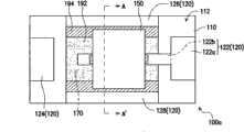
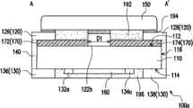
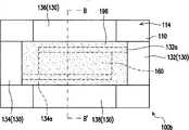
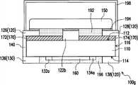
图1A为本发明的一实施例的一种保护元件的俯视示意图。图1B为图1A的保护元件的仰视示意图。图1C为图1A的保护元件沿线A-A’的剖面示意图。请同时参考图1A、图1B以及图1C,在本实施例中,保护元件100a包括一基板110、一上电极120、一下电极130、一端电极140、一金属块150、一加热器160以及一第一绝缘层170。FIG. 1A is a schematic top view of a protection element according to an embodiment of the present invention. FIG. 1B is a schematic bottom view of the protection element in FIG. 1A . Fig. 1C is a schematic cross-sectional view of the protection element in Fig. 1A along the line A-A'. Please refer to FIG. 1A, FIG. 1B and FIG. 1C at the same time. In this embodiment, the
详细而言,基板110具有彼此相对的一第一表面112与一第二表面114以及连接第一表面112与第二表面114的一侧表面116。在本实施例中,基板110的材质包括陶瓷(例如氧化铝)、二氧化锆(ZrO2)、氮化硅(Si3N4)、氮化铝(AlN)、氮化硼(BN)或是其他无机材料。In detail, the
上电极120配置于基板110的第一表面112上,且具有彼此相对的一第一子电极122与一第二子电极124以及彼此相对的一第三子电极126与一第四子电极128。需注意的是,于其他实施例中,上电极120也可不包含第二子电极124,且不影响过电流及过电压保护效果。较佳地,第一子电极122具有一本体部122a以及一与本体部122a相连接的第一延伸部122b,其中第一延伸部122b位于第三子电极126与第四子电极128之间。The
下电极130配置于基板110的第二表面114上。端电极140连接上电极120与下电极130,且覆盖基板110的部分侧表面116。在本实施例中,上电极120、下电极130与端电极140的材质例如为银、镍和金的多层堆迭结构,此外也可以银铂合金、镍合金、铜、锡等导电性质良好的材料来替代。The
金属块150配置于基板110的第一表面112上,且连接第三子电极126、第一延伸部122b与第四子电极128。此外,本实施例的金属块150的材质包括锡铅合金、锡银铅合金、锡铟铋铅合金、锡锑合金、锡银铜合金等低熔点合金。The
在本实施例中,加热器160配置于基板110的第二表面114上,且连接下电极130,其中第一延伸部122b延伸至加热器160的上方。特别是,加热器160在基板110的第一表面112上的正投影与第一子电极122的第一延伸部122b在基板110的第一表面112上的正投影至少部份重叠。此外,本实施例的下电极130具有彼此相对的一第五子电极132与一第六子电极134以及彼此相对的一第七子电极136与一第八子电极138。第五子电极132、第六子电极134、第七子电极136、第八子电极138依序对应第一子电极122、第二子电极124、第三子电极126以及第四子电极128配置。在本实施例中,第五子电极132具有一第二延伸部132a,第六子电极134具有一第三延伸部134a。第二延伸部132a与第三延伸部134a位于第七子电极136与第八子电极138之间并彼此不重叠,而加热器160连接于第二延伸部132a与第三延伸部134a之间。In this embodiment, the
然而,在其他实施例中,加热器160也可直接连接于第五子电极132和第六子电极134之间,而不需有第二延伸部132a与第三延伸部134a。更甚,再一实施例中,加热器160也可配置于基板110的第一表面112上,且连接于上电极120的第一子电极122和第二子电极124之间。此外,在本实施例中,加热器160的材质包括二氧化钌(RuO2)、碳黑粘着剂、铜、钛、镍铬合金与镍铜合金等,可分别利用厚膜印刷、溅镀、压合贴合或薄膜微影制程等形成。再者,为保护加热器160不受外界环境的污染或氧化,可在加热器160上覆盖一绝缘层196,其材质包括玻璃胶或环氧树脂(epoxy resin)等。However, in other embodiments, the
本实施例的保护元件100a的第一绝缘层170配置于基板110的第一表面112上,且具有不相连一第一低热传导部172以及一第二低热传导部174。特别是,第一低热传导部172位于加热器160与第三子电极126之间,而第二低热传导部174位于加热器160与第四子电极128之间。具体来说,本实施例的第一低热传导部172位于基板110与第三子电极126之间,而第二低热传导部174位于基板110与第四子电极128之间。第一低热传导部172与第二低热传导部174之间存在一第一间距D1,而第一子电极122的第一延伸部122b配置于第一间距D1中。此外,第一绝缘层170的材质例如是一玻璃材料或一高分子材料,具有比基板110低的热传导系数,较佳地,第一绝缘层170的热传导系数小于2W/(m·K)。举例来说,玻璃材料可包含例如二氧化硅(SiO2)、过氧化钠(Na2O3)、氧化硼(B2O3)、氧化镁(MgO)或氧化钙(CaO)等,其热传导系数可在1W/(m·K)至1.5W/(m·K)之间。而高分子材料则具有较低的热传导系数,例如是聚氨酯(polyurethane,PU)、聚酰亚胺(polyimide)、环氧树脂或紫外光型硬化树脂(UV curing resin),其中环氧树脂的热传导系数则在0.19W/(m·K)至0.6W/(m·K)之间。The first insulating
特别是,基板110的热传导系数大于第一绝缘层170的热传导系数。详细来说,在本实施例中,基板110相对于第一绝缘层170而言,可视为一高热传导绝缘层,而加热器160所产生的热可直接穿过基板110的中间区域而快速地传递至第一延伸部122b上。当然,基板110亦可与第一绝缘层170采用相同的材质,也就是说,基板110亦可视为一低热传导绝缘层,但由于基板110的厚度加上第一绝缘层170的厚度大于基板110本身的厚度,因此加热器160所产生的热大部份亦会穿过基板110的中间区域而快速地传递至第一延伸部122b上。换言之,基板110的材质可依使用需求而自行选择,其仍不影响本实施例的功效。In particular, the thermal conductivity of the
此外,为了提高金属块150熔断的效果,本实施例的保护元件100a更包括一助熔剂192配置于基板110的第一表面112上,并位于第一延伸部122b与第三子电极126之间,以及位于第一延伸部122b与第四子电极128之间。特别是,在本实施例之中,助熔剂192至少覆盖部分第一绝缘层170。具体来说,金属块150覆盖部分第三子电极126、助熔剂192、第一延伸部122b与第四子电极128。当加热器160加热而使助熔剂192与金属块150皆处于熔融状态时,因助熔剂192可避免金属块150受热熔融开始流动的表面在放置或一般电流通过时产生氧化薄膜,因此可以提高确保金属块150熔断的效果。此外,助熔剂192例如是由松脂、软化剂、活性剂以及合成橡胶所组成。In addition, in order to improve the melting effect of the
另外,在本实施例中,保护元件100a更包括一焊料层194于第三子电极126、第四子电极128与第一延伸部122b之上,通过固定金属块150于第三子电极126、第四子电极128与第一延伸部122b之上,并不以此为限,金属块150也可以习知的其他焊接技术固定而没有焊料层194。在本实施例中,焊料层194的材质可利用习知的焊接材料,例如锡银合金、锡铅合金等。In addition, in this embodiment, the
由于本实施例的保护元件100a具有第一绝缘层170,因此当加热器160加热并通过基板110将其所产生的热传递至上电极120时,一部分加热器160所产生的热会因为被基板110上的第一绝缘层170所阻挡而降低第三子电极126与第四子电极128所获得的热量,而另一部分加热器160所产生的热会直接经由第一子电极122而传递至金属块150,以使位于第一子电极122上方的金属块150熔断。也就是说,第三子电极126与第四子电极128因受低热传导绝缘层的阻挡,所以第三子电极126与第四子电极128上方的金属块150相较于第一子电极122上方的金属块150不易熔断,意即可减少金属块150的熔融量。因此,可将加热器160所产生的热视为集中地传递至第一子电极122,如此一来,除了可有效控制熔融态的金属块150的吸附面积,以获得稳定地熔断时间与模式外,亦可降低加热器160与第一子电极122于制作上对位偏差所产生的问题,意即可确保位于第一子电极122上方的金属块150可先熔断,而达到切断电路而达成有效防止过电压或过电流。Since the
另一方面,由于金属块150的熔化量减少,因此可缩短本实施例的保护元件100a在过电压保护作动所需时间,亦可降低熔融的金属块150导通第一延伸部122b与第三子电极126或第一延伸部122b与第四子电极128而产生短路的现象,而使本实施例的保护元件100a具有较佳的可靠度。On the other hand, since the amount of melting of the
此外,由于本实施例将第一延伸部122b设置于第一低热传导部172与第二低热传导部174之间存在的第一间距D1中,因此助熔剂192可有效地被引导到第一延伸部122b周围,而使第一延伸部122b具有较佳的润湿性,可确保金属块150熔断时间的稳定性。另外,由于保护元件100a具有第一绝缘层170,因此当保护元件100a为了搭配小尺寸的电子产品而缩小其元件体积时,上电极120的第一子电极122的第一延伸部122b亦能提供相应的电极面积,以可确保金属块150能迅速熔断。如此一来,除了可增加保护元件100a的应用范围外,亦可提高保护元件100a的可靠度。In addition, since the present embodiment disposes the
以下将利用多个不同的实施例来分别说明保护元件100b~100g的设计。在此必须说明的是,下述实施例沿用前述实施例的元件标号与部分内容,其中采用相同的标号来表示相同或近似的元件,并且省略了相同技术内容的说明。关于省略部分的说明可参考前述实施例,下述实施例中不再重复赘述。The design of the
图2A为本发明的另一实施例的一种保护元件的俯视示意图。图2B为图2A的保护元件的仰视示意图。图2C为图2A的保护元件沿线B-B’的剖面示意图。图2A至图2C的保护元件100b与图1A至图1C的保护元件100a相似,二者主要差异之处在于:图2A至图2C的保护元件100b的上电极120’的设计不同于保护元件100a的上电极120的设计。FIG. 2A is a schematic top view of a protection element according to another embodiment of the present invention. FIG. 2B is a schematic bottom view of the protection element in FIG. 2A . Fig. 2C is a schematic cross-sectional view of the protection element of Fig. 2A along the line B-B'. The
详细来说,第一子电极的122’的第一延伸部122b’的一部分位于第一间距D1’中,而第一延伸部122b’的另一部分位于第一绝缘层170的第一低热传导部172与第二低热传导部174上。具体来说,在本实施例中,由于第一间距D1’的距离大于第一间距D1,因此于制作上电极120’时,因受重力的影响而使得第一延伸部122b’产生一凹槽结构C,也就是说,第一延伸部122b’具有一位于第一间距D1中的凹槽结构C,使得第一子电极122’在相同的空间下产生立体结构,如此一来,可增加熔融态的金属块150的吸附面积。此外,助熔剂192亦可填入此凹槽结构C中,以使第一延伸部122b’更具有较佳的吸附熔融态的金属块150的能力。In detail, a part of the
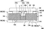
图3A为本发明的又一实施例的一种保护元件的俯视示意图。图3B为图3A的保护元件的仰视示意图。图3C为图3A的保护元件沿线C-C’的剖面示意图。图3A至图3C的保护元件100c与图1A至图1C的保护元件100a相似,二者主要差异之处在于:图3A至图3C的保护元件100c的的加热器160、第二延伸部222c、第三延伸部224a皆配置于基板110的第一表面112上,且保护元件100c更包括一第二绝缘层180a,其中第二绝缘层180a的热传导系数大于第一绝缘层170a的热传导系数。FIG. 3A is a schematic top view of a protection element according to another embodiment of the present invention. FIG. 3B is a schematic bottom view of the protection element of FIG. 3A . FIG. 3C is a schematic cross-sectional view of the protection element in FIG. 3A along the line C-C'. The
详细而言,第一子电极222具有一本体部222a以及一与本体部222a相连接的第一延伸部222b。在本实施例中,上电极220的第一子电极222更具有一第二延伸部222c,而第二子电极224具有一第三延伸部224a。第二延伸部222c与第三延伸部224a配置于第三子电极226与第四子电极228之间,而加热器160位于基板110的第一表面112上且连接第二延伸部222c与第三延伸部224a。在此必须说明的是,第一延伸部222b、第二延伸部222c、第三延伸部224a于基板110的第一表面112上的正投影彼此不重叠。In detail, the
特别是,本实施例的保护元件100c的第二绝缘层180a配置于加热器160与第一子电极222的第一延伸部222b之间,其中第一低热传导部172a连接第二低热传导部174a,而加热器160位于第二绝缘层180a与第一绝热层170a之间。详细来说,本实施例的第一绝缘层170a更包括一第三低热传导部176a以及一第四低热传导部178a,其中第三低热传导部176a连接第一低热传导部172a且延伸至第三延伸部224a上,而第四低热传导部178a连接第二低热传导部174a且延伸至第二延伸部222c上。在本实施例中,第三低热传导部176a与第四低热传导部178a之间存在一第二间距D2,而第二绝缘层180a配置于第二间距D2中,且部分第二绝缘层180a位于第三低热传导部176a与第四低热传导部178a上。此外,为使加热器160所产生的热可大部分传递到第一延伸部222b,第二绝缘层180a的材料选择以其热传导系数大于第一绝热层170a的热传导系数的8倍以上较佳。举例来说,在本实施例中,第二绝缘层180a的材质可例如是一陶瓷材料,而陶瓷材料例如是热传导系数在28W/(m·K)至40W/(m·K)之间的氧化铝(Al2O3)、50W/(m·K)至60W/(m·K)之间的氮化硼(BN)或160W/(m·K)至230W/(m·K)之间的氮化铝(AlN)。较佳地,第二绝缘层180a的热传导系数范围介于8W/(m·K)至80W/(m·K)之间。In particular, the second insulating
由于本实施例的保护元件100c的第二绝缘层180a位于第一延伸部222b与加热器160之间,因此当加热器160加热时,加热器160所产生的热大部分皆会直接传递至第一延伸部222b而使得位于第一延伸部222b上的金属块150快速熔断,以减少金属块150的熔化量,并达到切断电路而达成有效防止过电压或过电流。另一方面,由于金属块150的熔化量减少,因此可缩短本实施例的保护元件100c在过电压保护作动所需时间,亦可降低熔融的金属块150导通第一延伸部222b与第三子电极226或第一延伸部222b与第四子电极228而产生短路的现象,而使本实施例的保护元件100c具有较佳的可靠度。Since the second insulating
另外,由于保护元件100c同时具有第一绝缘层170a以及第二绝缘层180a,因此,当保护元件100c为了搭配小尺寸的电子产品而缩小其元件体积时,上电极220的第一子电极222的第一延伸部222b亦能提供相应的电极面积,以可确保金属块150能迅速熔断。如此一来,除了可增加保护元件100c的应用范围外,亦可提高保护元件100c的可靠度。In addition, since the
值得注意的是,在本实施例中,保护元件100c的下电极230具有依序对应第一子电极222、第二子电极224、第三子电极226以及第四子电极228配置的一第五子电极232、一第六子电极234、一第七子电极236与一第八子电极238。在另一实施例中,下电极230亦可依设计需求而没有第五子电极232,以在基板110的第二表面114上形成空脚位设计,提高保护元件组装于电路板(未显示)的摆放方向正确度。端电极240连接上电极220与下电极230,且覆盖基板110的部分侧表面116。It should be noted that, in this embodiment, the
图4A为本发明的再一实施例的一种保护元件的俯视示意图。图4B为图4A的保护元件的仰视示意图。图4C为图4A的保护元件沿线D-D’的剖面示意图。图4A至图4C的保护元件100d与图3A至图3C的保护元件100c相似,二者主要差异之处在于:图4A至图4C的保护元件100d的第一绝缘层170b以及第二绝缘层180b的配置位置不同于图3A至图3C的保护元件100c的第一绝缘层170a以及第二绝缘层180a的配置位置。FIG. 4A is a schematic top view of a protection element according to yet another embodiment of the present invention. FIG. 4B is a schematic bottom view of the protection element of FIG. 4A . FIG. 4C is a schematic cross-sectional view of the protection element in FIG. 4A along the line D-D'. The
详细来说,第三低热传导部176b与第四低热传导部178b配置于第二绝缘层180b上,且第三低热传导部176b与第四低热传导部178b之间存在一第二间距D2’,而第一子电极222的第一延伸部222b配置于该第二间距中D2’。由于本实施例的保护元件100d同时具有第一绝缘层170b与第二绝缘层180b,因此当加热器160加热时,一部分加热器160所产生的热会为第三低热传导部176b与第四低热传导部178b所阻挡,而减少热量传递至第三低热传导部176b与第四低热传导部178b上方的金属块150,而另一部分加热器160所产生的热会直接透过第二绝缘层180b、第一延伸部222b而传递至金属块150,以使位于第一延伸部222b上方的金属块150熔断。如此一来,可减少金属块150的熔融量,以缩短本实施例的保护元件100d在过电压保护作动所需时间,同时达到切断电路而达成有效防止过电压或过电流。In detail, the third low
图5为本发明的另一实施例的一种保护元件的剖面示意图。图5的保护元件100e与图1C的保护元件100a相似,二者主要差异之处在于:图5的保护元件100e通过改变基板210的设计来代替图1的第一绝缘层170所达到的效能。Fig. 5 is a schematic cross-sectional view of a protection element according to another embodiment of the present invention. The
详细来说,本实施例的基板210具有相连的一第一绝缘区块213与一第二绝缘区块215,其中第二绝缘区块215环绕第一绝缘区块213,且第一绝缘区块213与第二绝缘区块215实质上共平面,且第一子电极122的第一延伸部122b位于第一绝缘区块213,而第三子电极126与第四子电极128位于第二绝缘区块215。基板210具有彼此相对的一第一表面212与一第二表面214以及连接第一表面212与第二表面214的一侧表面216。端电极140连接上电极120与下电极130,且覆盖基板210的部分侧表面216。助熔剂192配置于基板210的第一表面212上,并位于第一子电极122的第一延伸部122b与第三子电极126之间以及位于第一子电极122的第一延伸部122b与第四子电极128之间,其中助熔剂192覆盖部分第二绝缘区块215。特别是,本实施例的第一绝缘区块213的热传导系数大于第二绝缘区块215的热传导系数。In detail, the
具体来说,在本实施例中,第一导绝缘区块213的材质例如是一陶瓷材料,而陶瓷材料例如是氧化铝(Al2O3)、氮化硼(BN)或氮化铝(AlN)。第一绝缘区块213的热传导系数范围介于8W/(m·K)至80W/(m·K)之间,较佳地,第一绝缘区块213的热传导系数范围介于8W/(m·K)至40W/(m·K)之间。另一方面,第二绝缘区块215的材质例如是一玻璃材料或一高分子材料,其中玻璃材料例如是二氧化硅、过氧化钠、氧化硼、氧化镁或氧化钙,而高分子材料例如是聚氨酯、聚酰亚胺、环氧树脂或紫外光型硬化树脂(UVcuring resin)。较佳地,第二绝缘区块215的热传导系数小于2W/(m·K)。Specifically, in this embodiment, the material of the first conductive insulating
由于加热器160位于第一绝缘区块213上,因此当加热器160加热时,加热器160所产生的热大部分皆会直接传递至第一延伸部122b而使得位于第一延伸部122b上的金属块150快速熔断,可减少金属块150的熔化量,并达到切断电路而达成有效防止过电压或过电流。于另一方面,由于金属块150的熔化量减少,因此可缩短本实施例的保护元件100e在过电压保护作动所需时间,亦可降低熔融的金属块150导通第一延伸部122b与第三子电极126或第一延伸部122b与第四子电极128而产生短路的现象,而使本实施例的保护元件100e具有较佳的可靠度。Since the
图6为本发明的又一实施例的一种保护元件的剖面示意图。图6的保护元件100f与图5的保护元件100e相似,二者主要差异之处在于:图6的保护元件100f的基板210a的第一绝缘区块213a与第二绝缘区块215a实质上不共平面。Fig. 6 is a schematic cross-sectional view of a protection element according to another embodiment of the present invention. The
详细来说,第一绝缘区块213a与第二绝缘区块215a之间具有一凹槽V,第一延伸部122b的一部分配置于凹槽V中且位于第一绝缘区块213a上,而第一延伸部122b的另一部分位于第二绝缘区块215a上。具体来说,在本实施例中,由于第一绝缘区块213a与第二绝缘区块215a之间具有凹槽V,因此于制作上电极120时,因受重力的影响而使得第一延伸部122b产生一凹槽结构C’,如此一来,第一子电极122在相同的空间下产生立体结构,可增加熔融态的金属块150的吸附面积。此外,助熔剂192亦可填入此凹槽结构C’中,以使第一延伸部122b更具有较佳的吸附熔融态的金属块150的能力。再者,熔融态的金属块150会因凹槽结构C’而产生毛细现象,有助于熔断金属块150,而达到切断电路而达成有效防止过电压或过电流。In detail, there is a groove V between the first insulating
图7为本发明的再一实施例的一种保护元件的剖面示意图。请参考图7,在本实施例中,图7的保护元件100g与图1A~图1C的保护元件100a相似,二者主要差异之处在于:图7的保护元件100g包括一壳体198。详细而言,壳体198配置于基板110的第一表面112上,且覆盖金属块150,用以保护金属块150,且可避免熔融态的金属块150、助熔剂192以及焊料层194流漏出来而发生电路干扰等问题。此外,壳体198的材质包括氧化铝、聚二醚酮(PEEK)、尼龙(nylon)、热塑性树脂、紫外光型硬化树脂或酚甲醛树脂等材料。Fig. 7 is a schematic cross-sectional view of a protection element according to yet another embodiment of the present invention. Please refer to FIG. 7 , in this embodiment, the
图8为本发明的更一实施例的一种保护元件的剖面示意图。请参考图8,在本实施例中,图8的保护元件100h与图7的保护元件100g相似,二者主要差异之处在于:图8的保护元件100h更包括一金属线250,其中金属线250在基板110的第一表面112上的正投影与第一延伸部122b在基板110的第一表面112上的正投影至少部份重叠。FIG. 8 is a schematic cross-sectional view of a protection element according to another embodiment of the present invention. Please refer to FIG. 8, in this embodiment, the
具体来说,金属线250是配置于金属块150的上方并部份接触金属块150,其中金属块150固定于第一子电极122上,且金属线250的形状例如是弧形(未示出)。金属线250与金属块150之间配置助熔剂260,来作为引导熔融的金属块150流动的媒介,而助熔剂260的材料除可使用与助熔剂192相同的松脂等材料外,亦可为一焊料层或其组合。在此必须说明的是,金属线250的外表面需与熔融的金属块150具有较佳的润湿性(Wetting)与吸附性(例如焊锡性(Solderability)),因此金属线250的材质可为金属或合金,例如是银、锡、铜、铜银合金、或铜镍锡合金等,或是由具有良好焊锡性的外金属层和具有较佳热传导的内金属层所组成,例如铜镀银、铜镀镍、铜镀锡、镍镀锡、铜镀金等材料。Specifically, the
由于本实施例的保护元件100h具有金属线250,因此当加热器160加热而使金属块150呈现熔融状态时,熔融的金属块150会因表面张力与毛细现象的缘故而吸附于所接触的金属线250上,且可进一步往第一延伸部122b流动,来达到切断电路而达成有效防止过电压或过电流。也就是说,熔融的金属块150经由金属线250的吸附,不易导通第一延伸部122b与第三子电极126或第一延伸部122b与第四子电极128,故可避免保护元件100h产生短路的现象,使其具有较佳的可靠度。Since the
值得一提的是,上述的实施例仅为举例说明,在其他未示出的实施中,本领域的技术人员当可参照前述实施例的说明,依据实际需求而选用前述构件或加以组合,以达到所需的技术效果。It is worth mentioning that the above-mentioned embodiments are only for illustration. In other unshown implementations, those skilled in the art can refer to the description of the above-mentioned embodiments and select or combine the above-mentioned components according to actual needs, so as to achieve the desired technical effect.
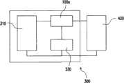
图9为本发明的一实施例的一种电子装置的方块示意图。请参考图9,由上述实施例所述的的保护元件100a(或保护元件100b~100g)可以与一电池310以及一侦测控制器330耦接而组合成一电子装置300。详细来说,电子装置300例如是一可携式电子产品的储能装置,当电子装置300外接一电源供应器420时可对电子装置300中的电池310进行充放电作业。在本实施例中,电池310耦接至保护元件100a。侦测控制器330耦接至保护元件100a,其中侦测控制器330例如是一集成电路(IC)晶片及一金属氧化物场效应管(MOSFET)。电源供应器420耦接至保护元件100a,用以提供一电源至电池310。FIG. 9 is a schematic block diagram of an electronic device according to an embodiment of the present invention. Please refer to FIG. 9 , the
当侦测控制器330侦测到电池电压过高时,侦测控制器330会将此过高电压(未示出)施加于保护元件100a的加热器160(请参考图1C),以熔断金属块150(请参考图1C)。再者,当电源供应器420提供一过电流(未示出)通过保护元件100a时,保护元件100a中的金属块150会因过电流通过而自动加热熔断。由于,在本实施例中,电子装置300是采用上述的保护元件100a(或保护元件100b~100g),因此除了可确实切断电路而达成有效防止过电压或过电流外,亦可避免保护元件100a产生短路的现象,使电子装置300具有较佳的可靠度。When the
虽然本发明已以实施例揭露如上,然其并非用以限定本发明,任何所属技术领域中具有通常知识者,在不脱离本发明的精神和范围内,当可作些许更动与润饰,故本发明的保护范围当以申请专利范围所界定者为准。Although the present invention has been disclosed above with the embodiments, it is not intended to limit the present invention. Anyone with ordinary knowledge in the technical field can make some changes and modifications without departing from the spirit and scope of the present invention. The scope of protection of the present invention shall be defined by the scope of the patent application.
Claims (25)
Priority Applications (1)
| Application Number | Priority Date | Filing Date | Title |
|---|---|---|---|
| CN201010189167.9ACN102263396B (en) | 2010-05-24 | 2010-05-24 | Protective components and electronic devices |
Applications Claiming Priority (1)
| Application Number | Priority Date | Filing Date | Title |
|---|---|---|---|
| CN201010189167.9ACN102263396B (en) | 2010-05-24 | 2010-05-24 | Protective components and electronic devices |
Publications (2)
| Publication Number | Publication Date |
|---|---|
| CN102263396A CN102263396A (en) | 2011-11-30 |
| CN102263396Btrue CN102263396B (en) | 2014-05-07 |
Family
ID=45009916
Family Applications (1)
| Application Number | Title | Priority Date | Filing Date |
|---|---|---|---|
| CN201010189167.9AActiveCN102263396B (en) | 2010-05-24 | 2010-05-24 | Protective components and electronic devices |
Country Status (1)
| Country | Link |
|---|---|
| CN (1) | CN102263396B (en) |
Families Citing this family (2)
| Publication number | Priority date | Publication date | Assignee | Title |
|---|---|---|---|---|
| JP7340979B2 (en)* | 2019-07-22 | 2023-09-08 | デクセリアルズ株式会社 | Protection elements and protection circuits |
| JP7393898B2 (en)* | 2019-09-04 | 2023-12-07 | デクセリアルズ株式会社 | protection element |
Citations (1)
| Publication number | Priority date | Publication date | Assignee | Title |
|---|---|---|---|---|
| CN101399100A (en)* | 2007-09-25 | 2009-04-01 | 乾坤科技股份有限公司 | Thermistor chip and method for manufacturing same |
Family Cites Families (2)
| Publication number | Priority date | Publication date | Assignee | Title |
|---|---|---|---|---|
| JP2001057139A (en)* | 1999-08-18 | 2001-02-27 | Uchihashi Estec Co Ltd | Protector for electronic/electrical apparatus and manufacture thereof |
| JP2004214033A (en)* | 2002-12-27 | 2004-07-29 | Sony Chem Corp | Protection element |
- 2010
- 2010-05-24CNCN201010189167.9Apatent/CN102263396B/enactiveActive
Patent Citations (1)
| Publication number | Priority date | Publication date | Assignee | Title |
|---|---|---|---|---|
| CN101399100A (en)* | 2007-09-25 | 2009-04-01 | 乾坤科技股份有限公司 | Thermistor chip and method for manufacturing same |
Non-Patent Citations (1)
| Title |
|---|
| JP特开2001-57139A 2001.02.27 |
Also Published As
| Publication number | Publication date |
|---|---|
| CN102263396A (en) | 2011-11-30 |
Similar Documents
| Publication | Publication Date | Title |
|---|---|---|
| US6566995B2 (en) | Protective element | |
| US6462318B2 (en) | Protective element | |
| US8675333B2 (en) | Protective device | |
| CN102362328B (en) | protection element | |
| US8767368B2 (en) | Protective element and method for producing the same | |
| JP6437253B2 (en) | Protective element and mounting body | |
| US20110057761A1 (en) | Protective device | |
| US9025295B2 (en) | Protective device and protective module | |
| CN110911389B (en) | Semiconductor module | |
| US20220199346A1 (en) | Protective element | |
| KR20170009840A (en) | Protective element and battery pack | |
| CN102263396B (en) | Protective components and electronic devices | |
| CN109727833B (en) | Protection element and circuit protection device thereof | |
| CN102237674B (en) | Protective components and electronic devices | |
| TWI452592B (en) | Protective device and electronic device | |
| US10892130B2 (en) | Protection device and circuit protection apparatus containing the same | |
| JP2009070803A (en) | Temperature fuse with resistor and battery protection circuit board | |
| JP4738953B2 (en) | Resistive fuse | |
| CN102035185B (en) | Protective element and its manufacturing method | |
| TWI385696B (en) | Protective component | |
| TW201505064A (en) | Protection element and electronic apparatus | |
| KR101354096B1 (en) | Protective device | |
| JP2005285439A (en) | Self-recovery protection element | |
| JP2005302546A (en) | Self-recovery protection element |
Legal Events
| Date | Code | Title | Description |
|---|---|---|---|
| C06 | Publication | ||
| PB01 | Publication | ||
| C10 | Entry into substantive examination | ||
| SE01 | Entry into force of request for substantive examination | ||
| C14 | Grant of patent or utility model | ||
| GR01 | Patent grant |