CN102262904A - Multi-bit 3D Mask Programmable Memory - Google Patents
Multi-bit 3D Mask Programmable MemoryDownload PDFInfo
- Publication number
- CN102262904A CN102262904ACN2010101949504ACN201010194950ACN102262904ACN 102262904 ACN102262904 ACN 102262904ACN 2010101949504 ACN2010101949504 ACN 2010101949504ACN 201010194950 ACN201010194950 ACN 201010194950ACN 102262904 ACN102262904 ACN 102262904A
- Authority
- CN
- China
- Prior art keywords
- storage element
- film
- mprom
- resistive
- resistive film
- Prior art date
- Legal status (The legal status is an assumption and is not a legal conclusion. Google has not performed a legal analysis and makes no representation as to the accuracy of the status listed.)
- Granted
Links
Images


Landscapes
- Semiconductor Memories (AREA)
Abstract
Description
Translated fromChinese技术领域technical field
本发明涉及集成电路领域,更确切地说,涉及掩膜编程存储器。This invention relates to the field of integrated circuits, and more specifically, to mask programmed memories.
背景技术Background technique
掩膜编程存储器(mask-programmable read-only memory,简称为mask-ROM)是指在生产过程中,尤其是光刻工艺中录入数据的存储器。三维掩膜编程存储器(three-dimensional mask-programmable memory,简称为3D-MPROM)是一种含有多个相互叠置掩膜编程存储层的mask-ROM。与其它mask-ROM相比,3D-MPROM具有极大的容量和极低的成本。Mask-programmable read-only memory (referred to as mask-ROM for short) refers to the memory for entering data in the production process, especially in the photolithography process. Three-dimensional mask-programmable memory (referred to as 3D-MPROM) is a mask-ROM containing multiple overlapping mask programming storage layers. Compared with other mask-ROMs, 3D-MPROM has enormous capacity and extremely low cost.
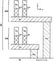
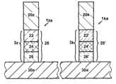
中国专利“三维只读存储器及其制造方法”(专利号:ZL98119572.5)提出了多种3D-MPROM。图1描述了一种典型3D-MPROM。它含有一个半导体衬底0s和一个3D-MPROM堆0。半导体衬底0s里的晶体管构成3D-MPROM的周边电路。3D-MPROM堆0堆叠在衬底0s上。在这个例子中,3D-MPROM堆0含有两个存储层100、200,存储层200叠置在存储层100上。每个存储层(如100)上含有多条地址线(如20a、20b、30a...)和多个3D-MPROM存储元(简称为3D-MPROM元)(如1aa、1ab...)。接触通道孔(如30av、30av’)将存储层(如100、200)和衬底0s耦合。The Chinese patent "Three-dimensional ROM and its manufacturing method" (Patent No.: ZL98119572.5) proposes various 3D-MPROMs. Figure 1 describes a typical 3D-MPROM. It contains a semiconductor substrate 0s and a 3D-
以往技术中,大多数3D-MPROM采用二进制,即3D-MPROM元具有两种状态‘1’和‘0’:处于状态‘1’的存储元(‘1’存储元)能导通电流,而处于状态‘0’的存储元(‘0’存储元)则不能。每个二进制3D-MPROM元可以存储1位信息。In the past technology, most 3D-MPROMs use binary, that is, 3D-MPROM elements have two states '1' and '0': the storage element in state '1' ('1' storage element) can conduct current, while A memory cell in state '0' ('0' memory cell) cannot. Each binary 3D-MPROM cell can store 1 bit of information.
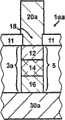
如图2A所示,‘1’存储元1aa含有一条高地址线20a、一层ROM膜3a和一条低地址线30a。ROM膜3a含有准导通膜5。该准导通膜5具有非线性电阻特性,它在一个方向上的导电性好于另一方向。准导通膜5一般采用二极管。这里,它是一个p-i-n二极管,并含有p膜12、i膜14和n膜16。准导通膜5也可以是其它二极管,如pn二极管、肖特基二极管等。由于在绝缘介质11中含有通道孔18,当在高地址线20a上加读电压时,在低地址线30a上能测到读电流。这对应于状态‘1’。As shown in FIG. 2A, a '1' memory cell 1aa includes an
如图2B所示,‘0’存储元1ba含有一条高地址线20b、一层ROM膜3b和一条低地址线30a。ROM膜3b含有绝缘介质膜11。由于在绝缘介质11中不含有通道孔,当在高地址线20b上加读电压时,在低地址线30a上不能测到读电流。这对应于状态‘0’。As shown in FIG. 2B, the '0' memory cell 1ba includes an
除二进制外,3D-MPROM也可以采用N(N为正整数且N>2)进制,即3D-MPROM元具有N种状态,处于不同状态的存储元具有不同的伏-安特性。每个N进制3D-MPROM元可以存储b位信息。这里,b=log2(N);b可以是整数,也可以是非整数。中国专利申请“N进制掩膜编程存储器”(专利申请号:200610100860.8)描述了多种N进制3D-MPROM,包括结形状型N进制3D-MPROM和结特性型N进制3D-MPROM。In addition to binary, 3D-MPROM can also use N (N is a positive integer and N>2) system, that is, 3D-MPROM elements have N states, and memory elements in different states have different V-A characteristics. Each N-ary 3D-MPROM element can store b-bit information. Here, b=log2 (N); b can be an integer or a non-integer. Chinese patent application "N-ary mask programming memory" (patent application number: 200610100860.8) describes a variety of N-ary 3D-MPROMs, including junction-shaped N-ary 3D-MPROMs and junction-characteristic N-ary 3D-MPROMs .
在结形状型N进制3D-MPROM中,不同状态的存储元具有不同的结构,如不同的结形状。如图2C所示,一个结形状型存储元1ca含有一条高地址线20c、一层ROM膜3c和一条低地址线30a。ROM膜3c含有一层绝缘介质11、一个部分通道孔18’和一层准导通膜5。与图2A相比,部分通道孔18’只能将高地址线20c和准导通膜5部分耦合。相应地,存储元1ca与存储元1aa具有不同的伏-安特性。In the junction-shaped N-ary 3D-MPROM, memory cells in different states have different structures, such as different junction shapes. As shown in FIG. 2C, a junction type memory cell 1ca includes an
在结特性型N进制3D-MPROM中,不同状态的存储元具有不同的结特性,如不同的掺杂浓度。如图2D所示,一个结特性型存储元1da含有一条高地址线20d、一层ROM膜3d和一条低地址线30a。ROM膜3d与存储元1aa中的ROM膜3a(图2A)具有类似的结构,它们均含有p-i-n二极管。但是,ROM膜3d的二极管5’与ROM膜3a的二极管5具有不同的掺杂浓度。这可以通过光刻和离子注入来实现。相应地,存储元1da与存储元1aa具有不同的伏-安特性。In the junction-type N-ary 3D-MPROM, memory elements in different states have different junction characteristics, such as different doping concentrations. As shown in FIG. 2D, a junction characteristic type memory cell 1da includes an
本分明进一步改进了上述专利申请的实施方法,以便在更大的范围(如~4.5V或更大)内调节存储元的伏-安曲线,从而实现多位元(如4位元)。在本说明书中,b位元(b-bit-per-cell)是指每个存储元能存储b位信息,如4位元存储器中每个存储元能存储4位信息。相应地,本分明提出一种多位元三维掩膜编程存储器(large bit-per-cell 3D-MPROM,简称为3D-MPROMB)。The present invention further improves the implementation method of the above-mentioned patent application so as to adjust the voltage-ampere curve of the storage element in a larger range (such as ~4.5V or greater), thereby realizing multi-bit (such as 4-bit). In this specification, b-bit-per-cell means that each storage cell can store b-bit information, for example, each storage cell in a 4-bit memory can store 4-bit information. Correspondingly, the present invention clearly proposes a multi-bit three-dimensional mask programming memory (large bit-per-cell 3D-MPROM, referred to as 3D-MPROMB for short).
发明内容Contents of the invention
本发明的主要目的是提供一种具有超大容量的三维掩膜编程存储器。The main purpose of the present invention is to provide a three-dimensional mask programming memory with super large capacity.
本发明的另一目的是提供一种具有超低成本的三维掩膜编程存储器。Another object of the present invention is to provide a three-dimensional mask programmed memory with ultra-low cost.
本发明的另一目的是提供一种每个存储元可以存储多位(如4位或更多)信息的三维掩膜编程存储器。Another object of the present invention is to provide a three-dimensional mask programming memory in which each memory cell can store multiple bits (eg, 4 bits or more) of information.
根据这些以及别的目的,本发明提供一种多位元三维掩膜编程存储器(3D-MPROMB),其每个存储元能存储多位(如4位)信息。3D-MPROMB通过在存储元中增加电阻膜和/或电阻元素来增大存储元伏-安曲线可调节的范围。相应地,3D-MPROMB可以分为含有电阻膜的3D-MPROMB(3D-MPROMBwith resistive layer,简称为3D-MPROMRL)和含有电阻元素的3D-MPROMB(3D-MPROMB with resistive element,简称为3D-MPROMRE)。According to these and other objects, the present invention provides a multi-bit three-dimensional mask programming memory (3D-MPROMB ), each memory cell of which can store multi-bit (eg, 4-bit) information. 3D-MPROMB increases the adjustable range of the voltage-ampere curve of the memory cell by adding a resistive film and/or a resistive element in the memory cell. Correspondingly, 3D-MPROMB can be divided into 3D-MPROMB with resistive layer (3D-MPROMB with resistive layer, referred to as 3D-MPROMRL for short) and 3D-MPROMB with resistive elements (3D-MPROMB with resistive layer element, referred to as 3D-MPROMRE ).
本发明的3D-MPROMB包括:一个含有晶体管的半导体衬底;多个叠置在衬底并与衬底耦合的掩膜编程存储层,每个存储层含有包括第一存储元和第二存储元的多个掩膜编程存储元,每个存储元含有准导通膜,该准导通膜在一个方向上的导电性好于另一方向,所述多个存储元具有N(N>2)种状态,不同状态下的存储元具有不同的伏-安特性;所述第一存储元的阈值电压在所有状态中最小;所述第二存储元的阈值电压大于所述第一存储元,所述第二存储元比所述第一存储元至少多含有一层电阻膜。The 3D-MPROMB of the present invention includes: a semiconductor substrate containing transistors; a plurality of mask programming storage layers stacked on the substrate and coupled with the substrate, each storage layer includes a first storage unit and a second storage A plurality of mask programming storage elements of the unit, each storage unit contains a quasi-conducting film, and the conductivity of the quasi-conducting film in one direction is better than that in the other direction, and the plurality of storage units have N (N>2 ) states, the memory cells in different states have different volt-ampere characteristics; the threshold voltage of the first memory cell is the smallest among all states; the threshold voltage of the second memory cell is greater than that of the first memory cell, The second memory cell contains at least one more layer of resistive film than the first memory cell.
本发明的3D-MPROMB还包括:一个含有晶体管的半导体衬底;多个叠置在衬底并与衬底耦合的掩膜编程存储层,每个存储层含有包括第一存储元和第二存储元的多个掩膜编程存储元,每个存储元含有准导通膜,该准导通膜在一个方向上的导电性好于另一方向,所述多个存储元具有N(N>2)种状态,不同状态下的存储元具有不同的伏-安特性;所述第一存储元的阈值电压在所有状态中最小;所述第二存储元的阈值电压大于所述第一存储元,所述第二存储元的准导通膜比所述第一存储元的准导通膜含有更高的电阻元素浓度。The 3D-MPROMB of the present invention also includes: a semiconductor substrate containing transistors; a plurality of mask programming storage layers stacked on the substrate and coupled with the substrate, each storage layer contains a first storage element and a second storage element. A plurality of mask-programmed memory cells for memory cells, each memory cell containing a quasi-conductive film having better conductivity in one direction than the other, the plurality of memory cells having N (N> 2) Two states, the memory cells in different states have different volt-ampere characteristics; the threshold voltage of the first memory cell is the smallest among all states; the threshold voltage of the second memory cell is greater than that of the first memory cell , the quasi-conducting film of the second memory cell contains a higher resistance element concentration than the quasi-conducting film of the first memory cell.
附图说明Description of drawings
图1是表示一种3D-MPROM的断面图;Fig. 1 is a sectional view showing a kind of 3D-MPROM;
图2A-图2D是表示以往技术中‘1’3D-MPROM元、‘0’3D-MPROM元、结形状型N进制3D-MPROM元、结特性型N进制3D-MPROM元的断面图;Figures 2A-2D are cross-sectional views showing '1' 3D-MPROM elements, '0' 3D-MPROM elements, junction shape N-ary 3D-MPROM elements, and junction characteristic type N-ary 3D-MPROM elements in the prior art ;
图3表示一种4位元3D-MPROMB(b=4,N=16)中16种状态的伏-安特性;Fig. 3 represents the volt-ampere characteristic of 16 kinds of states in a kind of 4-bit 3D-MPROMB (b=4, N=16);
图4A-图4D是表示几种含有电阻膜3D-MPROMB(3D-MPROMRL)元的断面图;Fig. 4A-Fig. 4D are the sectional views showing several kinds of 3D-MPROMB (3D-MPROMRL ) elements containing resistive film;
图5比较基元、电阻膜和3D-MPROMRL元的伏-安曲线;Figure 5 compares the volt-ampere curves of the element, the resistive film and the 3D-MPROMRL element;
图6A-图6D是表示四种电阻膜的断面图;6A-FIG. 6D are cross-sectional views representing four kinds of resistive films;
图7是表示一种3D-MPROMRL采用的电阻膜掩膜版的俯视图,以及在工艺流程中电阻膜图形和高低地址线图形的相对位置;Figure 7 is a top view of a resistive film mask used in 3D-MPROMRL , and the relative positions of the resistive film pattern and the high and low address line patterns in the process flow;
图8A-图8C表示一种3D-MPROMRL元的工艺流程。该图中的结构是沿图7中AA’线的断面图;8A-8C show a process flow of a 3D-MPROMRL element. The structure in this figure is a sectional view along the AA' line in Fig. 7;
图9A-图9C是表示三种含有部分电阻膜3D-MPROMB元的断面图;Fig. 9A-Fig. 9C are the sectional views showing three kinds of 3D-MPROMB elements containing part of the resistive film;
图10是表示一种含有电阻元素3D-MPROMB(3D-MPROMRE)元的断面图;Fig. 10 is a sectional view showing a 3D-MPROMB (3D-MPROMRE ) element containing a resistance element;
图11比较硅二极管、SiOx(x<2)二极管和SiO2膜的伏-安曲线;Fig. 11 compares the volt-ampere curve of silicon diode, SiOx (x<2) diode and SiO2 film;
图12A和图12B表示3D-MPROMRE元的一种工艺流程;12A and 12B represent a process flow of 3D-MPROMRE element;
图13A-图13C是表示三种2位元3D-MPROMB(b=2,N=4)的断面图;13A-FIG. 13C are sectional views showing three kinds of 2-bit 3D-MPROMB (b=2, N=4);
图14A是表示一种2位元3D-MPROMB的电路图;图14B是表示一种读操作时字线和位线电压的时序图;Fig. 14A is a circuit diagram showing a 2-bit 3D-MPROMB ; Fig. 14B is a timing diagram showing a word line and a bit line voltage during a read operation;
图15A是表示一种4位元3D-MPROMB(b=4,N=16)状态设置的表格;图15B是表示一种4位元3D-MPROMB的断面图。FIG. 15A is a table showing a state setting of a 4-bit 3D-MPROMB (b=4, N=16); FIG. 15B is a cross-sectional view showing a 4-bit 3D-MPROMB.
除图15A以外,本说明书附图未按比例绘制。With the exception of Figure 15A, the drawings of this specification are not drawn to scale.
具体实施方式Detailed ways
本发明提供一种多位元三维掩膜编程存储器(3D-MPROMB),其每个存储元能存储多位(如4位)信息。图3是一种4位元3D-MPROMB(b=4,N=16)中16种状态的伏-安曲线410-425。它们与状态‘0’-‘f’一一对应。注意该图的电流轴采用指数刻度。当流过存储元中的电流超过阈值电流(IT)时,存储元导通,这时存储元上的电压为阈值电压(VT)。例如,状态‘0’的阈值电压为VT0;...;状态‘f’的阈值电压为VTf。本说明书采用以下规范:具有较小VT的存储元被赋予较小的状态值,如具有最小VT的存储元处于状态‘0’;具有第二小VT的存储元处于状态‘1’;...。当然,采用其它规范也是可行的。The present invention provides a multi-bit three-dimensional mask programming memory (3D-MPROMB ), each storage unit of which can store multi-bit (eg 4-bit) information. FIG. 3 is a volt-ampere curve 410-425 of 16 states in a 4-bit 3D-MPROMB (b=4, N=16). They correspond to states '0'-'f' one by one. Note that the current axis of the graph is on an exponential scale. When the current flowing through the storage element exceeds the threshold current (IT ), the storage element is turned on, and the voltage on the storage element is the threshold voltage (VT ). For example, the threshold voltage of state '0' is VT0 ; ...; the threshold voltage of state 'f' is VTf . This specification adopts the following specification: the storage element with the smaller VT is assigned a smaller state value, such as the storage element with the smallest VT is in state '0'; the storage element with the second smallest VT is in state '1';…. Of course, it is also feasible to adopt other specifications.
为了容忍工艺变化和读出误差,相邻状态VT的间隔ΔVT一般需要~0.3V或更大,因此VT窗口-即最大VT(VTf)和最小VT(VT0)之差-一般需要~4.5V或更大。为了实现这么大的VT窗口,本发明提出在存储元中增加电阻膜和/或电阻元素。相应地,3D-MPROMB可以分为含有电阻膜的3D-MPROMB(3D-MPROMRL)和含有电阻元素的3D-MPROMB(3D-MPROMRE)。To tolerate process variations and readout errors, the separation ΔVT between adjacent states VT generally needs to be ~0.3V or greater, so the VT window—that is, the difference between the maximum VT (VTf ) and the minimum VT (VT0 ) - Typically ~4.5V or greater is required. In order to realize such a large VT window, the present invention proposes adding a resistive film and/or a resistive element in the storage element. Correspondingly, 3D-MPROMB can be divided into 3D-MPROMB (3D-MPROMRL ) containing a resistive film and 3D-MPROMB (3D-MPROMRE ) containing a resistive element.
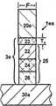
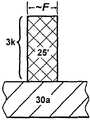
3D-MPROMRL的例子见图4A-图9C。其中,图4A-图4D描述了多种3D-MPROMRL元。如图4A所示,该存储元是一个基元1za。基元1za在所有状态中具有最小的VT-VT0。它含有多层膜,包括高地址线20z、ROM膜3z和低地址线30a。这些膜一起被称为基膜。其中,地址线20z、30a含有导体材料,如高掺杂的多晶硅(poly Si)、钨(W)、钛钨合金(TiW)、氮化钛(TiN)、铜(Cu)等。ROM膜3z只含有准导通膜25。准导通膜25具有非线性电阻特性,它在一个方向上的导电性好于另一方向。准导通膜25一般采用二极管。这里,它是一个p-i-n二极管,并含有p膜22、i膜24和n膜26。有关准导通膜的细节可参考中国专利ZL98119572.5。Examples of 3D-MPROMRL are shown in Figures 4A-9C. Among them, FIG. 4A-FIG. 4D describe various 3D-MPROMRL elements. As shown in FIG. 4A, the storage element is a primitive 1za. Primitive 1za has the smallest VT −VT0 among all states. It contains a multi-layer film including
图4B描述了第一种3D-MPROMRL元1ea。它含有高地址线20e、ROM膜3e和低地址线30a。地址线20e、30a含有导体材料。ROM膜3e除了准导通膜25(包括p膜22、i膜24和n膜26)以外,还含有一层电阻膜23。在该实施例中,电阻膜23位于准导通膜25之上。在IT时,电阻膜23的电阻最好接近或大于准导通膜25的电阻。由于基元1za除地址线20z、30a外只含有准导通膜25,因此电阻膜23的电阻最好接近或大于基元1za的电阻。Figure 4B depicts the first 3D-MPROMRL element 1ea. It contains
图4C描述了第二种3D-MPROMRL元1fa。它含有高地址线20f、ROM膜3f和低地址线30a。地址线20f、30a含有导体材料。ROM膜3f除了准导通膜25(包括p膜22、i膜24和n膜26)以外,还含有一层电阻膜23。在该实施例中,电阻膜23位于准导通膜25之中,即位于最高层的p膜22和中间的i膜24之间。类似地,在IT时,电阻膜23的电阻最好接近或大于基元1za的电阻。FIG. 4C depicts the second 3D-MPROMRL element 1fa. It contains upper address line 20f, ROM film 3f and
图4D描述了第三种3D-MPROMRL元1ga。它含有高地址线20g、ROM膜3g和低地址线30a。地址线20g、30a含有导体材料。ROM膜3g除了准导通膜25(包括p膜22、i膜24和n膜26)以外,还含有一层电阻膜23。在该实施例中,电阻膜23位于准导通膜25之下。类似地,在IT时,电阻膜23的电阻最好接近或大于基元1za的电阻。Figure 4D depicts the third 3D-MPROMRL element 1ga. It contains an
为了形成三维结构(即多个存储层能相互叠置),在同一存储层上的3D-MPROMRL元(1ea/1fa/1ga。这里,“/”表示“或”)和基元1za需要为上面的存储层提供一个良好的基础。也就是说,它们的高地址线(20e/20f/20g、20z)最好可以被平面化(如采用化学机械抛光法,即CMP方法)。这需要电阻膜23的厚度TR满足以下要求:1)在图4C和图4D的实施例中,如果ROM膜(3f/3g、3z)还需要被平面化,TR应该小于基元1za中准导通膜25最高层膜22的厚度TU;2)在图4B-图4D的实施例中,如果ROM膜(3e/3f/3g、3z)不需要被平面化,则TR应该小于基元1za中高地址线20z的厚度TA。In order to form a three-dimensional structure (that is, multiple storage layers can be stacked on top of each other), the 3D-MPROMRL element (1ea/1fa/1ga. Here, "/" means "or") and the primitive 1za on the same storage layer need to be The storage layer above provides a good foundation. That is to say, their high address lines (20e/20f/20g, 20z) can preferably be planarized (such as by chemical mechanical polishing, that is, CMP method). This requires the thicknessTR of the
图5比较了基元1za、电阻膜23和3D-MPROMRL元1ea的伏-安曲线。它们分别以430、431和432表示。由于在3D-MPROMRL元1ea中,电阻膜23和准导通膜25串联在一起,因此3D-MPROMRL元1ea的伏-安曲线432是由准导通膜25(也就是基元1za)的伏-安曲线430偏移而成,偏移量由电阻膜23的伏-安曲线431决定:在IT时,3D-MPROMRL元1ea的VT是基元1za的VT0与电阻膜23上的电压Vr之和,即VT=VT0+Vr。FIG. 5 compares the voltage-ampere curves of the element 1za, the
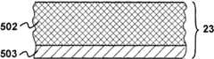
图6A-图6D是四种电阻膜的断面图。其中,图6A中的电阻膜23只含有一层核心电阻膜502。该核心电阻膜502具有图5所示的指数型伏-安特性。它含有一层半导体膜,和/或一个薄的介质膜。半导体材料可以是硅(Si)、碳(C)、锗(Ge)、碳硅化合物(SiC)、锗硅化合物(SiGe)等;它最好具有非单晶结构,如无定形结构、微晶结构或多晶结构。半导体膜的一个例子是45nm的非定形硅,它可以将存储元VT偏移~4.5V或更多。介质膜可以是氧化硅(SiO2)、氮化硅(Si3N4)或其它保护性陶瓷材料(参见中国专利ZL98119257.2)。虽然介质膜传统上被认为是绝缘膜,但当其厚度很薄时,它具有指数型伏-安特性。因此,介质膜适合用于电阻膜。介质膜的例子包括5nm的氧化硅、或9nm的氮化硅,这些介质膜都可以将VT偏移~4.5V或更多。6A-6D are cross-sectional views of four kinds of resistive films. Wherein, the
图6B-图6D描述了其它三种电阻膜23。在图6B中,核心电阻膜502上方含有一层隔离膜501;在图6C中,核心电阻膜502下方含有一层隔离膜503;在图6D中,核心电阻膜502上下方各含有一层隔离膜501、503。隔离膜为电阻膜23提供一个更好的界面,它还可以作为刻蚀停止膜。一般说来,隔离膜含有导体材料,如高掺杂的多晶硅(poly Si)、钨(W)、钛钨合金(TiW)、氮化钛(TiN)、铜(Cu)等。6B-6D describe other three kinds of
图7是表示一种用于3D-MPROMRL的电阻膜掩膜版的俯视图,以及在工艺流程中电阻膜图形7x、7y和高地址线图形20a、20b、20e及低地址线图形30a、30b的相对位置。相对于高地址线图形的特征尺寸1F,电阻膜图形的特征尺寸可以更大,为nF(n>1,最好~2)。而且,相邻的电阻膜图形(如7ab、7bb)还可以合并在一起以形成一个电阻膜图形7y。因此,电阻膜掩膜版是一个nF掩膜版(n>1,最好~2)。例如,20nm节点的3D-MPROMRL可以采用40nm节点的电阻膜掩膜版。Fig. 7 is a top view showing a resistive film mask plate for 3D-MPROMRL , and
图8A-图8C表示一种3D-MPROMRL元1ea的工艺流程。它包括如下步骤:A)形成低地址线30a,然后淀积准导通膜25,并将其刻蚀成为多个柱体25(图8A);B)淀积并平面化层内介质27。之后,淀积电阻膜23并利用图7中的电阻膜掩膜版进行图形转换,然后刻蚀电阻膜23。注意到电阻膜23的尺寸为nF(n>1,最好~2)(图8B);C)淀积高地址线膜20e(图8C)并将其刻蚀。该刻蚀步骤以层内介质27作为刻蚀停止膜,以清除部分电阻膜23。因此,在最后的存储元结构中,电阻膜23与高地址线20e自对准(图4B)。对于熟悉本专业的人士来说,图4C和图4D中的3D-MPROMRL元1fa、1ga也可以采用类似步骤完成。8A-8C show a process flow of a 3D-MPROMRL element 1ea. It includes the following steps: A) forming the
根据以上对工艺流程的描述,电阻膜23的最后形状由电阻膜图形7x和高地址线图形20e的重叠部分决定。这个自对准的工艺流程对电阻膜图形的边缘精度要求较低。也就是说,20nm节点的3D-MPROMRL不仅可以采用40nm节点的电阻膜掩膜版(图7),而且该掩膜版还可以是一个非高精度的掩膜版。因此,3D-MPROMRL的掩膜版成本能被极大地降低。最后,由于上述工艺流程对高地址线和电阻膜之间的对准精度要求较低,所以3D-MPROMRL的光刻工艺成本也相对较低。According to the above description of the process flow, the final shape of the
3D-MPROMRL可以与结形状型N进制3D-MPROM(参见中国专利申请200610100860.8)结合,即通过改变电阻膜的形状来实现更多种的状态。相应地,本发明还提出一种含有部分电阻膜的3D-MPROM(3D-MPROMB with partialresistive layer,简称为3D-MPROMPRL)。图9A-图9C描述了三种3D-MPROMPRL元。3D-MPROMRL can be combined with junction-shaped N-ary 3D-MPROM (see Chinese patent application 200610100860.8), that is, more states can be realized by changing the shape of the resistive film. Correspondingly, the present invention also proposes a 3D-MPROM with a partial resistive layer (3D-MPROMB with partial resistive layer, 3D-MPROMPRL for short). Figures 9A-9C describe three 3D-MPROMPRL elements.
如图9A所示,3D-MPROMPRL元1ha含有高地址线20h、ROM膜3h和低地址线30a。其中,ROM膜3h含有阻挡介质膜29、部分电阻膜23’和准导通膜25。阻挡介质膜29和部分电阻膜23’位于准导通膜25上方。高地址线20h通过部分电阻膜23’仅与准导通膜25部分耦合。由于部分电阻膜23’与图4B中的电阻膜23具有不同形状-部分电阻膜23’比电阻膜23小,因此存储元1ha的电阻比图4B中存储元1ea的电阻大。具体说来,部分电阻膜23’和准导通膜25之间的接触面积21小于准导通膜25的截面积,而图4B中电阻膜23和准导通膜25之间的接触面积和准导通膜25的截面积接近。通过改变接触面21的宽度f,可以导致不同的电阻,从而形成更多种的状态。由于f由电阻膜图形决定,因此一个电阻膜掩膜版就可以将多位信息录入至每个存储元。类似地,在IT时,部分电阻膜23’的电阻最好接近或大于基元1za的电阻。很明显,中国专利申请200610100860.8中的各种发明精神均可以应用至3D-MPROMPRL。As shown in FIG. 9A, the 3D-MPROMPRL cell 1ha contains an
图9B和图9C描述了另外两种3D-MPROMPRL元1ia、1ja。它们类似于图9A中3D-MPROMPRL元1ha。唯一的差别是其部分电阻膜23’的位置:在图9B中部分电阻膜23’位于准导通膜25中;在图9C中部分电阻膜23’位于准导通膜25下。类似地,通过改变f的数值,可以导致不同的电阻,从而形成更多种的状态。这样,一个电阻膜掩膜版就可以将多位信息录入至每个存储元。Figure 9B and Figure 9C describe two other 3D-MPROMPRL elements 1ia, 1ja. They are similar to 3D-MPROMPRL element 1ha in Fig. 9A. The only difference is the position of part of the resistive film 23': part of the resistive film 23' is located in the
在一个含有电阻元素的3D-MPROMB(3D-MPROMRE)中,3D-MPROMRE元的准导通膜比基元的准导通膜含有更高的电阻元素浓度。图10-图12B描述了多种3D-MPROMRE。如图10所示,3D-MPROMRE元1ka含有高地址线20k、ROM膜3k和低地址线30a。其中,ROM膜3k含有准导通膜25’。与其左边的基元1za比较,3D-MPROMRE元1ka的准导通膜25’与基元1za的准导通膜25具有类似结构,即均为p-i-n二极管。但是,准导通膜25’比准导通膜25含有更高的电阻元素浓度。在与基元1za中准导通膜25(如p-i-n二极管)的半导体材料(如硅)结合后,电阻元素(如氧、氮、碳等)能增大该半导体材料的电阻率,而且电阻元素的浓度增加导致电阻率增加。这与半导体材料中常用的掺杂元素(如硼、磷、砷)不同:这些掺杂元素降低半导体的电阻率,而且掺杂元素的浓度增加导致电阻率降低。In a 3D-MPROMB (3D-MPROMRE ) containing resistive elements, the quasi-conducting film of the 3D-MPROMRE element contains a higher concentration of resistive elements than the quasi-conducting film of the elementary element. Figures 10-12B describe various 3D-MPROMREs . As shown in FIG. 10, the 3D-MPROMRE element 1ka includes an
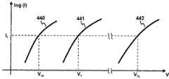
图11比较了硅二极管(即基元)、SiOx(x<2)二极管(即3D-MPROMRE元)和SiO2膜的伏-安曲线。它们分别以440、441和442表示。很明显,SiOx(x<2)二极管的伏-安曲线441应位于硅二极管伏-安曲线440和SiO2膜伏-安曲线442之间。这是因为SiO2是SiOx(x<2)的一种极端情况:当SiOx(x<2)中氧的含量高到一定程度时,SiOx就变成了SiO2。因此,SiOx(x<2)二极管的VT应介于硅二极管的VT0和SiO2膜的VTx之间,即VT0<VT<VTx。由于VTx数值极大,3D-MPROMRE元的VT可以在极大范围内调节。与氧类似,氮也可以在极大范围内调节3D-MPROMRE元的VT。另外,碳也可以用来调节VT。这是因为碳能与硅形成SiCz(z<1)。SiCz作为一种半导体材料,其能带隙(bandgap)比硅宽。一般说来,二极管中半导体材料的能带隙越宽,该二极管的VT越高。Figure 11 compares the volt-ampere curves of silicon diodes (ie primitives),SiOx (x<2) diodes (ie 3D-MPROMRE elements) and SiO2 films. These are indicated at 440, 441 and 442, respectively. Obviously, the
图12A和图12B表示3D-MPROMRE元1ka的一种工艺流程。首先形成低地址线30a和准导通膜25。然后通过一个电阻元素掩膜版在光刻胶28中形成开口28o。电阻元素掩膜版与电阻膜掩膜版类似,都是nF掩膜版(n>1,最好~2)。这里,开口28o的宽度为nF(n>1,最好~2),比高地址线20k的宽度(~F)大。接着通过离子注入法在准导通膜25中注入电阻元素(如氧、氮、碳等)(图12A)。该离子注入步骤能增加开口28o下电阻元素的浓度。之后,清除光刻胶28并将准导通膜25刻蚀成柱体25’(图12B)。余下的步骤与基元1za类似(参见图8B和图8C)。与3D-MPROMRL类似,20nm节点的3D-MPROMRE不仅可以采用40nm节点的电阻元素掩膜版,而且该掩膜版还可以是一个非高精度的掩膜版。综上所述,3D-MPROMB的信息录入成本远比大多数人想象的要低。12A and 12B show a process flow of 3D-MPROMRE element 1ka. First, the
3D-MPROMRL(图4B-图4D、图9A-图9C)、3D-MPROMRE(图10)可以和结形状型N进制3D-MPROM、结特性型N进制3D-MPROM(参见中国专利申请200610100860.8)结合起来,进一步提高每个存储元存储的信息量。图13A-图14B描述多种2位元3D-MPROMB(b=2,N=4);图15A和图15B描述一种4位元3D-MPROMB(b=4,N=16)。3D-MPROMRL (Figure 4B-Figure 4D, Figure 9A-Figure 9C), 3D-MPROMRE (Figure 10) can be combined with junction shape type N-ary 3D-MPROM, junction characteristic type N-ary 3D-MPROM (see China Patent application 200610100860.8) combined to further increase the amount of information stored in each storage element. 13A-14B describe various 2-bit 3D-MPROMB (b=2, N=4); FIG. 15A and FIG. 15B describe a 4-bit 3D-MPROMB (b=4, N=16).
图13A-图13C描述三种2位元3D-MPROMB。如图13A所示,该实施例结合了图4B中的3D-MPROMRL和图10中的3D-MPROMRE。这四个存储元1za、1ma、1na、1oa代表四种状态。基元1za不含任何电阻膜或电阻元素。存储元1ma的准导通膜25’至少含有一种电阻元素。存储元1na在准导通膜25上含有一层电阻膜23。存储元1oa含有电阻元素和电阻膜。另外,存储元1ma可以与基元1za具有不同的掺杂浓度。很明显,该实施例只需要2个掩膜版(即电阻膜掩膜版和电阻元素掩膜版)就能将2位信息录入至每个存储元。13A-13C describe three kinds of 2-bit 3D-MPROMB . As shown in FIG. 13A , this embodiment combines the 3D-MPROMRL in FIG. 4B and the 3D-MPROMRE in FIG. 10 . These four storage elements 1za, 1ma, 1na, and 1oa represent four states. Element 1za does not contain any resistive film or resistive elements. The quasi-conducting film 25' of the memory cell 1ma contains at least one resistance element. The memory cell 1na includes a
图13B表示第二种2位元3D-MPROMB。它采用了图4B中3D-MPROMRL的两种实施例。这四个存储元1za、1pa、1qa、1ra代表四种状态。例如,存储元1pa的电阻膜23a含有15nm非定形硅,存储元1qa的电阻膜23b含有30nm非定形硅,存储元1ra含有电阻膜23a和23b,即45nm非定形硅。又如,存储元1pa的电阻膜23a含有3nm氮化硅,存储元1qa的电阻膜23b含有6nm氮化硅,存储元1ra则含有9nm氮化形硅。类似地,该实施例只需要2个电阻膜掩膜版就能将2位信息录入至每个存储元。FIG. 13B shows the second type of 2-bit 3D-MPROMB . It adopts two embodiments of 3D-MPROMRL in Fig. 4B. These four storage elements 1za, 1pa, 1qa, and 1ra represent four states. For example, the
图13C表示第三种2位元3D-MPROMB。它结合了图4B和图4D中3D-MPROMRL的两种实施例。这四个存储元1za、1sa、1ta、1ua代表四种状态。存储元1sa的电阻膜23c位于准导通膜25上方,存储元1ta的电阻膜23d位于准导通膜25下方,存储元1ua含有两层电阻膜23c和23d,它们分别位于准导通膜25上方和下方。该实施例也只需要2个电阻膜掩膜版就能将2位信息录入至每个存储元。FIG. 13C shows the third type of 2-bit 3D-MPROMB . It combines two embodiments of 3D-MPROMRL in Fig. 4B and Fig. 4D. The four storage elements 1za, 1sa, 1ta, and 1ua represent four states. The
在对3D-MPROMB进行读操作时,需要提供一系列逐步增大的读电压信号。一旦读电压大到能在一存储元中产生读电流,则产生一输出信号,这时的读电压对应于该存储元所处的状态。图14A和图14B描述了一种2位元3D-MPROMB的读电路和读操作。When performing a read operation on the 3D-MPROMB , it is necessary to provide a series of gradually increasing read voltage signals. Once the read voltage is large enough to generate a read current in a memory element, an output signal is generated, and the read voltage at this time corresponds to the state of the memory element. 14A and 14B describe a read circuit and read operation of a 2-bit 3D-MPROMB.
如图14A所示,该2位元3D-MPROMB包括两部分:存储堆0和周边电路0K。存储堆0包括数据组30DT(包括数据元1ca-1cz、数据位线30a-30z)和哑元组32DY(包括哑元1c0-1c3、哑位线32a-32d)。数据元存储数据,而哑元为读操作提供参考信号。数据元和哑元都具有4种状态‘0’-‘3’。例如,数据元1ca和哑元1c1都处于状态‘1’。该图中括号里的数字表示存储元所处的状态。在该实施例中,处于相同状态的哑元和数据元具有相同结构并采用相同材料。这样哑元不会导致额外的生产成本,因此能降低3D-MPROMB的成本。As shown in FIG. 14A, the 2-bit 3D-MPROMB includes two parts:
周边电路0K形成在衬底0s里,并通过接触通道孔与存储堆0耦合。它含有字线电压产生电路50、行译码器52、列译码器54、参考信号产生电路56、读出放大器58、数据缓冲器60和N进制-二进制转换器62等。字线电压产生电路50在不同读阶段产生不同的读电压。行译码器52根据行地址52A将该读电压送到相应的字线(如20c)。列译码器54根据列地址54A将相应的位线与读出放大器58的第一输入51耦合。参考信号产生电路56为读出放大器58产生参考电压53。它含有多个开关对(如56a’),每个开关对含有一对共享栅信号(如56a)的晶体管。The peripheral circuit OK is formed in the substrate 0s, and is coupled with the
图14B表示一种读操作时字线和位线电压的时序图。每个读操作需要含有N-1个读阶段。该实施例含有3个读阶段:T0-T2。在每个读阶段,在选中的字线(如20c)上加相应的读电压。根据存储元(1ca-1cz、1c0-1c3)所处的状态,不同存储元流过不同的读电流,这样与其耦合的位线上(30a-30z、32a-32d)的电压也以不同速率上升。当每个读阶段快结束时,数据组30DT中所有数据位线(30a-30z)上的电压被一一读出。如果位线(如30a)电压大于触发电压Vx,则输出55变高。同时,读出放大器58将相应位线(30a)在剩余读操作中设置为高电压VH,这样能避免剩余读操作中的读电压损坏相应存储元(1ca)中的二极管。以下介绍各个读阶段的细节:Figure 14B shows a timing diagram of word line and bit line voltages during a read operation. Each read operation needs to contain N-1 read phases. This embodiment contains 3 read phases: T0-T2. In each read phase, a corresponding read voltage is applied to the selected word line (eg, 20c). According to the states of the memory cells (1ca-1cz, 1c0-1c3), different memory cells flow different read currents, so the voltages on the bit lines (30a-30z, 32a-32d) coupled with them also rise at different rates . Towards the end of each read phase, the voltages on all the data bit lines (30a-30z) in the data set 30DT are read out one by one. If the bit line (
A)在第一读阶段T0中,在字线20c上加第一读电压VR0。这时,位线(30a-30z、32a-32d)电压根据存储元状态以不同速率上升。对于状态‘0’(如存储元1ca、1c0)来说,读电压VR0产生一大读电流,因此位线(30a、32a)电压上升很快;对于状态‘1’(如存储元1cz、1c1)来说,读电压VR0产生小读电流,因此位线(30z、32b)电压上升很慢;...。同时,参考信号产生电路56中仅栅信号56a被置高,开关对56a’闭合,这样哑位线32a、32b耦合在一起。因此,参考电压53是状态‘0’和状态‘1’位线电压的平均。当T0快结束时,读出放大器58将数据组30DT中所有数据位线(30a-30z)上的电压与参考电压53一一比较,输出55被送到数据缓冲器60。A) In the first read phase T0, a first read voltage VR0 is applied to the
B)在第二读阶段T1中,在字线20c上加第二读电压VR1。对于状态‘0’(如存储元1ca、1c0)来说,位线(30a、32a)在T0时已被设置为VH;对于状态‘1’(如存储元1cz、1c1)来说,读电压VR1产生一大读电流,因此位线(30z、32b)电压上升很快;对于状态‘2’(如存储元1cb、1c2)来说,读电压VR1产生小读电流,因此位线(30b、32c)电压上升很慢;...。同时,参考信号产生电路56中仅栅信号56b被置高,开关对56b’闭合,这样哑位线32b、32c耦合在一起。因此,参考电压53是状态‘1’和状态‘2’位线电压的平均。当T1快结束时,数据组30DT中所有数据位线(30a-30z)上的电压被一一读出,输出55被送到数据缓冲器60。B) In the second read phase T1, a second read voltage VR1 is applied to the
C)在第三读阶段T2中,在字线20c上加第三读电压VR2。对于状态‘0’和‘1’(如存储元1ca、1c0;1cz、1c1)来说,位线(30a、32a;30z、32b)在T0和T1时已被设置为VH;对于状态‘2’(如存储元1cb、1c2)来说,读电压VR2产生一大读电流,因此位线(30b、32c)电压上升很快;...。同时,参考信号产生电路56中仅栅信号56c被置高,开关对56c’闭合,这样哑位线32c、32d耦合在一起。因此,参考电压53是状态‘2’和状态‘3’位线电压的平均。当T2快结束时,数据组30DT中所有数据位线(30a-30z)上的电压被一一读出,输出55被送到数据缓冲器60。C) In the third read phase T2, a third read voltage VR2 is applied to the
D)在读操作结束时,存储在数据缓冲器60中的数据被N进制-2进制转换器62转换成二进制数据。这样,存储在存储元1ca-1cz中的4进制数据被读出。D) At the end of the read operation, the data stored in the
图15A和图15B描述一种4位元3D-MPROMB。图15A中的表格列出了其16种状态的设置;图15B是其断面图。对于熟悉本专业的人士来说,图14A和图14B中的读电路和读操作都可以应用到4位元3D-MPROMB中。15A and 15B describe a 4-bit 3D-MPROMB . The table in Figure 15A lists the settings of its 16 states; Figure 15B is its cross-sectional view. For those familiar with this field, the read circuit and read operation in Fig. 14A and Fig. 14B can be applied to 4-bit 3D-MPROMB.
如图15A所示,为了实现4位元,存储元可以在4维上变化:高电阻膜23x、中电阻膜23y、低电阻膜23z和电阻元素。表中的“是”表示采用电阻膜或电阻元素;“否”表示不采用。由于每维有两种选择(“是”和“否”),该实施例共有16种状态。这4维可以通过4个掩膜版来实现,即高电阻膜掩膜版、中电阻膜掩膜版、低电阻膜掩膜版和电阻元素掩膜版。As shown in FIG. 15A, in order to realize 4 bits, memory cells can be varied in 4 dimensions:
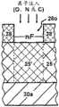
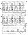
如图15B所示,该4位元3D-MPROMB含有一个半导体衬底0s和一个3D-MPROMB堆0。该半导体衬底0s含有多个晶体管0T(包括栅极0P)。这些晶体管0T及其互连层0I一起构成3D-MPROMB堆0的周边电路0X。3D-MPROMB堆0叠置在衬底0s上。在该实施例中,它含有4个存储层100-400:存储层100含有字线(80a-80h...)、位线(90d...)和存储元(1ad-1hd...);存储层200叠置与存储层100之上,并含有字线(80a-80h...)、位线(90d*...)和存储元(1ad*...);存储层300叠置与存储层200之上,并含有字线(80a’-80h’...)、位线(90d’...)和存储元(1a’d’-1h’d’...);存储层400叠置与存储层300之上,并含有字线(80a’-80h’...)、位线(90d”...)和存储元(1a’d”...)。接触通道孔(如90dv)将存储层(如100)与衬底0s耦合。As shown in FIG. 15B, the 4-bit 3D-MPROMB includes a semiconductor substrate 0s and a 3D-MPROMB stack 0. The semiconductor substrate Os includes a plurality of transistors OT (including gates OP). These transistors 0T and their interconnection layer 0I together constitute the peripheral circuit 0X of the 3D-MPROMB- stack 0. The 3D-MPROMB stack 0 is stacked on the substrate 0s. In this embodiment it contains 4 memory layers 100-400:
在存储层100、300中的存储元1ad-1hd、1a’d’-1h’d’分别代表状态‘0’-‘f’(参考图15A)。例如,存储元1ad代表状态‘0’,它是一个基元,即不含有任何电阻膜或电阻元素;存储元1bd代表状态‘1’,其二极管25’含有电阻元素;存储元1cd代表状态‘2’,它含有低电阻膜23z;存储元1ed代表状态‘4’,它含有中电阻膜23y;存储元1a’d’代表状态‘8’,它含有高电阻膜23x;存储元1h’d’代表状态‘f’,它含有高电阻膜23x、中电阻膜23y、低电阻膜23z和电阻元素;...。为简便计,存储层200、400中的存储元细节以及存储层200-400的接触通道孔没有画出。The storage cells 1ad-1hd, 1a'd'-1h'd' in the storage layers 100, 300 respectively represent states '0'-'f' (refer to FIG. 15A ). For example, storage unit 1ad represents state '0', which is a primitive, that is, does not contain any resistance film or resistance element; storage unit 1bd represents state '1', and its diode 25' contains resistance element; storage unit 1cd represents state' 2', it contains low-resistance film 23z; memory unit 1ed represents state '4', and it contains medium-resistance film 23y; memory unit 1a'd' represents state '8', and it contains high-
图15B中的实施例结合了多种改进的3D-MPROM,如混合层3D-MPROM(参见中国专利申请200610162698.2)和窄线宽3D-MPROM(参见中国专利申请200810183936.7)。混合层3D-MPROM中部分存储层(如100、200)共享地址线(80a-80h...);其它存储层(如200、300)则不共享地址线,而由层间介质膜121隔开。窄线宽3D-MPROM中存储层地址线的特征尺寸小于衬底晶体管栅极的特征尺寸。进一步结合三维存储模块(参见中国专利申请200710194280.4),一个采用20nm技术的x8x8x4 3D-MPROM模块可以存储~1TB信息。这里,x8x8x4是指该模块含有8个3D-MPROMB芯片,每个3D-MPROMB芯片含有8个存储层,每个存储元存储4位信息。The embodiment in FIG. 15B combines various improved 3D-MPROMs, such as mixed layer 3D-MPROM (see Chinese patent application 200610162698.2) and narrow linewidth 3D-MPROM (see Chinese patent application 200810183936.7). Some storage layers (such as 100, 200) in the hybrid layer 3D-MPROM share address lines (80a-80h...); other storage layers (such as 200, 300) do not share address lines, but are separated by interlayer dielectric films open. The characteristic size of the storage layer address line in the narrow line width 3D-MPROM is smaller than the characteristic size of the gate of the substrate transistor. Further combined with a three-dimensional memory module (see Chinese patent application 200710194280.4), a x8x8x4 3D-MPROM module using 20nm technology can store ~1TB of information. Here, x8x8x4 means that the module contains 8 3D-MPROMB chips, each 3D-MPROMB chip contains 8 storage layers, and each
在图13A-图13C中,只需要2个掩膜版就能将2位信息录入至每个存储元,即实现2位元;在图15A和图15B中,只需要4个掩膜版就能将4位信息录入至每个存储元,即实现4位元。实际上,在3D-MPROMB中,每个掩膜版能在存储元中多录入1位信息。譬如,5个掩膜版可以实现5位元,6个掩膜版可以实现6位元...。如果采用图9A-图9C中3D-MPROMPRL,掩膜版的数目还可以进一步减少。这比在以往技术的二进制3D-MPROM中,每多录入1位信息就需要多叠置一个存储层来说,节省了很多生产成本。In Figure 13A-Figure 13C, only 2 masks are needed to record 2 bits of information into each storage element, that is, 2 bits are realized; in Figure 15A and Figure 15B, only 4 masks are needed 4 bits of information can be entered into each storage element, that is, 4 bits are realized. In fact, in 3D-MPROMB , each mask can record 1 more bit of information in the storage element. For example, 5 masks can realize 5 bits, and 6 masks can realize 6 bits. … If the 3D-MPROMPRL shown in FIG. 9A-FIG. 9C is used, the number of masks can be further reduced. This saves a lot of production cost compared to the binary 3D-MPROM of the prior technology, which requires an additional storage layer to be stacked for every additional bit of information entered.
虽然以上说明书具体描述了本发明的一些实例,熟悉本专业的技术人员应该了解,在不远离本发明的精神和范围的前提下,可以对本发明的形式和细节进行改动,这并不妨碍它们应用本发明的精神。因此,除了根据附加的权利要求书的精神,本发明不应受到任何限制。Although the above description has specifically described some examples of the present invention, those skilled in the art should understand that the form and details of the present invention can be changed without departing from the spirit and scope of the present invention, which does not hinder their application. spirit of the invention. The invention, therefore, should not be restricted except in accordance with the spirit of the appended claims.
Claims (10)
Priority Applications (2)
| Application Number | Priority Date | Filing Date | Title |
|---|---|---|---|
| CN201010194950.4ACN102262904B (en) | 2010-05-24 | 2010-05-24 | Multi-bit 3D Mask Programmable Memory |
| CN201410050524.1ACN103794611B (en) | 2010-05-24 | 2010-05-24 | Many bits three-dimensional masking film program memorizer |
Applications Claiming Priority (1)
| Application Number | Priority Date | Filing Date | Title |
|---|---|---|---|
| CN201010194950.4ACN102262904B (en) | 2010-05-24 | 2010-05-24 | Multi-bit 3D Mask Programmable Memory |
Related Child Applications (1)
| Application Number | Title | Priority Date | Filing Date |
|---|---|---|---|
| CN201410050524.1ADivisionCN103794611B (en) | 2010-05-24 | 2010-05-24 | Many bits three-dimensional masking film program memorizer |
Publications (2)
| Publication Number | Publication Date |
|---|---|
| CN102262904Atrue CN102262904A (en) | 2011-11-30 |
| CN102262904B CN102262904B (en) | 2014-12-24 |
Family
ID=45009510
Family Applications (1)
| Application Number | Title | Priority Date | Filing Date |
|---|---|---|---|
| CN201010194950.4AExpired - Fee RelatedCN102262904B (en) | 2010-05-24 | 2010-05-24 | Multi-bit 3D Mask Programmable Memory |
Country Status (1)
| Country | Link |
|---|---|
| CN (1) | CN102262904B (en) |
Cited By (4)
| Publication number | Priority date | Publication date | Assignee | Title |
|---|---|---|---|---|
| CN103367365A (en)* | 2012-03-30 | 2013-10-23 | 成都海存艾匹科技有限公司 | Small grain three-dimensional memory |
| CN104576678A (en)* | 2013-10-15 | 2015-04-29 | 爱思开海力士有限公司 | Variable resistance memory apparatus, manufacturing method thereof |
| CN107978336A (en)* | 2016-10-24 | 2018-05-01 | 杭州海存信息技术有限公司 | Multi-bit three-dimensional offset printing memory |
| CN108806756A (en)* | 2016-04-14 | 2018-11-13 | 成都三维艾匹科技有限公司 | The three-dimensional one-time programming memory of multidigit member containing a plurality of umbral position line |
Citations (5)
| Publication number | Priority date | Publication date | Assignee | Title |
|---|---|---|---|---|
| CN1099695C (en)* | 1998-09-24 | 2003-01-22 | 张国飙 | Three-dimensional read-only memory and its manufacturing method |
| CN1412850A (en)* | 2001-10-07 | 2003-04-23 | 张国飙 | 3D integrated memory |
| CN1485925A (en)* | 1998-09-24 | 2004-03-31 | �ź㴫 | Read-only memory cell of three-dimensional memory |
| CN1897161A (en)* | 2005-07-15 | 2007-01-17 | 张国飙 | N-ary mask-programmable memory |
| CN101110269A (en)* | 2002-11-17 | 2008-01-23 | 张国飙 | Improved three-dimensional read-only memory |
- 2010
- 2010-05-24CNCN201010194950.4Apatent/CN102262904B/ennot_activeExpired - Fee Related
Patent Citations (5)
| Publication number | Priority date | Publication date | Assignee | Title |
|---|---|---|---|---|
| CN1099695C (en)* | 1998-09-24 | 2003-01-22 | 张国飙 | Three-dimensional read-only memory and its manufacturing method |
| CN1485925A (en)* | 1998-09-24 | 2004-03-31 | �ź㴫 | Read-only memory cell of three-dimensional memory |
| CN1412850A (en)* | 2001-10-07 | 2003-04-23 | 张国飙 | 3D integrated memory |
| CN101110269A (en)* | 2002-11-17 | 2008-01-23 | 张国飙 | Improved three-dimensional read-only memory |
| CN1897161A (en)* | 2005-07-15 | 2007-01-17 | 张国飙 | N-ary mask-programmable memory |
Cited By (6)
| Publication number | Priority date | Publication date | Assignee | Title |
|---|---|---|---|---|
| CN103367365A (en)* | 2012-03-30 | 2013-10-23 | 成都海存艾匹科技有限公司 | Small grain three-dimensional memory |
| CN103367365B (en)* | 2012-03-30 | 2015-09-02 | 成都海存艾匹科技有限公司 | Little grain three-dimensional memory |
| CN104576678A (en)* | 2013-10-15 | 2015-04-29 | 爱思开海力士有限公司 | Variable resistance memory apparatus, manufacturing method thereof |
| CN108806756A (en)* | 2016-04-14 | 2018-11-13 | 成都三维艾匹科技有限公司 | The three-dimensional one-time programming memory of multidigit member containing a plurality of umbral position line |
| CN107978336A (en)* | 2016-10-24 | 2018-05-01 | 杭州海存信息技术有限公司 | Multi-bit three-dimensional offset printing memory |
| CN107978336B (en)* | 2016-10-24 | 2020-04-10 | 杭州海存信息技术有限公司 | Multi-bit three-dimensional offset printing memory |
Also Published As
| Publication number | Publication date |
|---|---|
| CN102262904B (en) | 2014-12-24 |
Similar Documents
| Publication | Publication Date | Title |
|---|---|---|
| US8884376B2 (en) | Large bit-per-cell three-dimensional mask-programmable read-only memory | |
| JP5454945B2 (en) | Storage device | |
| US7706177B2 (en) | Method of programming cross-point diode memory array | |
| TWI445137B (en) | Single-time programmable memory, electronic system, electrical fuse memory, programmable resistive memory and method thereof | |
| US10002872B2 (en) | Three-dimensional vertical one-time-programmable memory | |
| US8624236B2 (en) | Phase change memory cell having vertical channel access transistor | |
| US8072791B2 (en) | Method of making nonvolatile memory device containing carbon or nitrogen doped diode | |
| US7800934B2 (en) | Programming methods to increase window for reverse write 3D cell | |
| CN103165607B (en) | Semiconductor storage unit and manufacture method thereof | |
| US10128313B2 (en) | Non-volatile memory device and structure thereof | |
| CN102446547A (en) | Programmable memory device with self-aligned intersection point and manufacturing method thereof | |
| US20080316808A1 (en) | Nonvolatile memory device containing carbon or nitrogen doped diode | |
| US7800939B2 (en) | Method of making 3D R/W cell with reduced reverse leakage | |
| US10559574B2 (en) | Three-dimensional vertical one-time-programmable memory comprising Schottky diodes | |
| TW202029191A (en) | Memory device and method for reading a memory device | |
| TW202243138A (en) | Semiconductor device | |
| CN102262904A (en) | Multi-bit 3D Mask Programmable Memory | |
| TW202522493A (en) | Memory device and forming method thereof | |
| US7759666B2 (en) | 3D R/W cell with reduced reverse leakage | |
| US20180137927A1 (en) | Three-Dimensional Vertical One-Time-Programmable Memory Comprising No Separate Diode Layer | |
| US11522011B2 (en) | Selector element with ballast for low voltage bipolar memory devices | |
| CN1770494B (en) | Chalcogenide memory | |
| TW202514628A (en) | Memory device and method for fabricating semiconductor device | |
| US10490562B2 (en) | Three-dimensional vertical one-time-programmable memory comprising multiple antifuse sub-layers | |
| TWI876562B (en) | Mram cell, nonvolatile memory structure and method of writing to mram cell |
Legal Events
| Date | Code | Title | Description |
|---|---|---|---|
| C06 | Publication | ||
| PB01 | Publication | ||
| C10 | Entry into substantive examination | ||
| SE01 | Entry into force of request for substantive examination | ||
| C14 | Grant of patent or utility model | ||
| GR01 | Patent grant | ||
| CP02 | Change in the address of a patent holder | ||
| CP02 | Change in the address of a patent holder | Address after:610041 B-36, 6 Yongfeng Road, Chengdu, Sichuan Patentee after:Zhang Guobiao Address before:610051 5A-001 box 59, Jianshe Road, Sichuan, Chengdu, China Patentee before:Zhang Guobiao Address after:610041 B-36, 6 Yongfeng Road, Chengdu, Sichuan Patentee after:Zhang Guobiao Address before:610051 5A-001 box 59, Jianshe Road, Sichuan, Chengdu, China Patentee before:Zhang Guobiao | |
| CF01 | Termination of patent right due to non-payment of annual fee | ||
| CF01 | Termination of patent right due to non-payment of annual fee | Granted publication date:20141224 Termination date:20190524 |