CN102254831A - High-precision ceramic substrate process - Google Patents
High-precision ceramic substrate processDownload PDFInfo
- Publication number
- CN102254831A CN102254831ACN2010101811848ACN201010181184ACN102254831ACN 102254831 ACN102254831 ACN 102254831ACN 2010101811848 ACN2010101811848 ACN 2010101811848ACN 201010181184 ACN201010181184 ACN 201010181184ACN 102254831 ACN102254831 ACN 102254831A
- Authority
- CN
- China
- Prior art keywords
- metal layer
- ceramic substrate
- conductive metal
- oxygen
- substrate process
- Prior art date
- Legal status (The legal status is an assumption and is not a legal conclusion. Google has not performed a legal analysis and makes no representation as to the accuracy of the status listed.)
- Pending
Links
- 239000000919ceramicSubstances0.000titleclaimsabstractdescription87
- 239000000758substrateSubstances0.000titleclaimsabstractdescription77
- 238000000034methodMethods0.000titleclaimsabstractdescription60
- 229910052751metalInorganic materials0.000claimsabstractdescription118
- 239000002184metalSubstances0.000claimsabstractdescription118
- 238000005530etchingMethods0.000claimsabstractdescription23
- 238000003466weldingMethods0.000claimsabstractdescription17
- 239000000843powderSubstances0.000claimsabstractdescription14
- 238000010344co-firingMethods0.000claimsabstractdescription10
- 239000011521glassSubstances0.000claimsabstractdescription9
- 238000007747platingMethods0.000claimsabstractdescription9
- PXHVJJICTQNCMI-UHFFFAOYSA-NNickelChemical compound[Ni]PXHVJJICTQNCMI-UHFFFAOYSA-N0.000claimsdescription16
- 230000003064anti-oxidating effectEffects0.000claimsdescription14
- TWNQGVIAIRXVLR-UHFFFAOYSA-Noxo(oxoalumanyloxy)alumaneChemical compoundO=[Al]O[Al]=OTWNQGVIAIRXVLR-UHFFFAOYSA-N0.000claimsdescription12
- 239000003795chemical substances by applicationSubstances0.000claimsdescription10
- 239000011651chromiumSubstances0.000claimsdescription6
- 229910052759nickelInorganic materials0.000claimsdescription6
- 238000005476solderingMethods0.000claimsdescription6
- PNEYBMLMFCGWSK-UHFFFAOYSA-Naluminium oxideInorganic materials[O-2].[O-2].[O-2].[Al+3].[Al+3]PNEYBMLMFCGWSK-UHFFFAOYSA-N0.000claimsdescription5
- PCHJSUWPFVWCPO-UHFFFAOYSA-NgoldChemical group[Au]PCHJSUWPFVWCPO-UHFFFAOYSA-N0.000claimsdescription5
- 229910052737goldInorganic materials0.000claimsdescription5
- 239000010931goldSubstances0.000claimsdescription5
- 230000003647oxidationEffects0.000claimsdescription5
- 238000007254oxidation reactionMethods0.000claimsdescription5
- 238000004537pulpingMethods0.000claimsdescription5
- 229910052709silverInorganic materials0.000claimsdescription5
- 239000004332silverSubstances0.000claimsdescription5
- VYZAMTAEIAYCRO-UHFFFAOYSA-NChromiumChemical compound[Cr]VYZAMTAEIAYCRO-UHFFFAOYSA-N0.000claimsdescription4
- BQCADISMDOOEFD-UHFFFAOYSA-NSilverChemical compound[Ag]BQCADISMDOOEFD-UHFFFAOYSA-N0.000claimsdescription4
- 229910000531Co alloyInorganic materials0.000claimsdescription3
- 229910000990Ni alloyInorganic materials0.000claimsdescription3
- QVYYOKWPCQYKEY-UHFFFAOYSA-N[Fe].[Co]Chemical compound[Fe].[Co]QVYYOKWPCQYKEY-UHFFFAOYSA-N0.000claimsdescription3
- KGWWEXORQXHJJQ-UHFFFAOYSA-N[Fe].[Co].[Ni]Chemical compound[Fe].[Co].[Ni]KGWWEXORQXHJJQ-UHFFFAOYSA-N0.000claimsdescription3
- 229910052804chromiumInorganic materials0.000claimsdescription3
- PMHQVHHXPFUNSP-UHFFFAOYSA-Mcopper(1+);methylsulfanylmethane;bromideChemical compoundBr[Cu].CSCPMHQVHHXPFUNSP-UHFFFAOYSA-M0.000claimsdescription3
- 229910000881Cu alloyInorganic materials0.000claimsdescription2
- CERQOIWHTDAKMF-UHFFFAOYSA-MMethacrylateChemical compoundCC(=C)C([O-])=OCERQOIWHTDAKMF-UHFFFAOYSA-M0.000claimsdescription2
- POUYTGMZOYRZNA-UHFFFAOYSA-N[Si].[Ni].[Cr].[Cu]Chemical compound[Si].[Ni].[Cr].[Cu]POUYTGMZOYRZNA-UHFFFAOYSA-N0.000claimsdescription2
- 229920000800acrylic rubberPolymers0.000claimsdescription2
- 238000005553drillingMethods0.000claims1
- 239000000853adhesiveSubstances0.000abstract1
- 230000001070adhesive effectEffects0.000abstract1
- 230000007547defectEffects0.000abstract1
- 239000002002slurrySubstances0.000abstract1
- 239000010410layerSubstances0.000description97
- 238000005516engineering processMethods0.000description13
- 238000009713electroplatingMethods0.000description9
- 238000004519manufacturing processMethods0.000description7
- 239000000463materialSubstances0.000description7
- 229910018072Al 2 O 3Inorganic materials0.000description6
- 238000000576coating methodMethods0.000description6
- 239000010949copperSubstances0.000description6
- 230000002950deficientEffects0.000description6
- 239000002699waste materialSubstances0.000description6
- PIGFYZPCRLYGLF-UHFFFAOYSA-NAluminum nitrideChemical compound[Al]#NPIGFYZPCRLYGLF-UHFFFAOYSA-N0.000description5
- RYGMFSIKBFXOCR-UHFFFAOYSA-NCopperChemical compound[Cu]RYGMFSIKBFXOCR-UHFFFAOYSA-N0.000description4
- QVGXLLKOCUKJST-UHFFFAOYSA-Natomic oxygenChemical compound[O]QVGXLLKOCUKJST-UHFFFAOYSA-N0.000description4
- 229910052802copperInorganic materials0.000description4
- 230000003287optical effectEffects0.000description4
- 229910052760oxygenInorganic materials0.000description4
- 239000001301oxygenSubstances0.000description4
- 239000002994raw materialSubstances0.000description4
- 238000005245sinteringMethods0.000description4
- QPLDLSVMHZLSFG-UHFFFAOYSA-NCopper oxideChemical compound[Cu]=OQPLDLSVMHZLSFG-UHFFFAOYSA-N0.000description3
- 239000005751Copper oxideSubstances0.000description3
- 229910010293ceramic materialInorganic materials0.000description3
- 239000011248coating agentSubstances0.000description3
- 229910000431copper oxideInorganic materials0.000description3
- 239000000126substanceSubstances0.000description3
- 125000005250alkyl acrylate groupChemical group0.000description2
- 229920001577copolymerPolymers0.000description2
- 238000011161developmentMethods0.000description2
- 230000000694effectsEffects0.000description2
- 150000002734metacrylic acid derivativesChemical class0.000description2
- 150000002739metalsChemical class0.000description2
- 238000012986modificationMethods0.000description2
- 230000004048modificationEffects0.000description2
- 238000007639printingMethods0.000description2
- 238000011160researchMethods0.000description2
- 238000004544sputter depositionMethods0.000description2
- 229910000967As alloyInorganic materials0.000description1
- 229910000599Cr alloyInorganic materials0.000description1
- 241000282414Homo sapiensSpecies0.000description1
- 229910021578Iron(III) chlorideInorganic materials0.000description1
- RTAQQCXQSZGOHL-UHFFFAOYSA-NTitaniumChemical compound[Ti]RTAQQCXQSZGOHL-UHFFFAOYSA-N0.000description1
- GZWXHPJXQLOTPB-UHFFFAOYSA-N[Si].[Ni].[Cr]Chemical compound[Si].[Ni].[Cr]GZWXHPJXQLOTPB-UHFFFAOYSA-N0.000description1
- 239000013543active substanceSubstances0.000description1
- 229910052782aluminiumInorganic materials0.000description1
- XAGFODPZIPBFFR-UHFFFAOYSA-NaluminiumChemical compound[Al]XAGFODPZIPBFFR-UHFFFAOYSA-N0.000description1
- 230000005540biological transmissionEffects0.000description1
- 239000003990capacitorSubstances0.000description1
- ORTQZVOHEJQUHG-UHFFFAOYSA-Lcopper(II) chlorideChemical compoundCl[Cu]ClORTQZVOHEJQUHG-UHFFFAOYSA-L0.000description1
- 230000007812deficiencyEffects0.000description1
- 230000005611electricityEffects0.000description1
- 230000008020evaporationEffects0.000description1
- 238000001704evaporationMethods0.000description1
- 239000007888film coatingSubstances0.000description1
- 238000009501film coatingMethods0.000description1
- 230000017525heat dissipationEffects0.000description1
- 230000020169heat generationEffects0.000description1
- 238000009413insulationMethods0.000description1
- RBTARNINKXHZNM-UHFFFAOYSA-Kiron trichlorideChemical compoundCl[Fe](Cl)ClRBTARNINKXHZNM-UHFFFAOYSA-K0.000description1
- 210000001161mammalian embryoAnatomy0.000description1
- 238000012536packaging technologyMethods0.000description1
- 238000012545processingMethods0.000description1
- 238000004080punchingMethods0.000description1
- 239000002344surface layerSubstances0.000description1
- 239000002562thickening agentSubstances0.000description1
- 239000010936titaniumSubstances0.000description1
- 229910052719titaniumInorganic materials0.000description1
- 238000001771vacuum depositionMethods0.000description1
- 238000009736wettingMethods0.000description1
Images


Landscapes
- Laminated Bodies (AREA)
- Electroplating Methods And Accessories (AREA)
Abstract
Description
Translated fromChinese技术领域technical field
本发明为有关一种高精密度陶瓷基板工艺,而高精密度陶瓷基板工艺必须以电镀及高准度曝光/蚀刻方式制作,有别于一般以印刷方式制作的陶瓷基板,尤其指陶瓷基板表面镀上金属层、导电金属层后,以氧化铝、玻璃粉及可真空烧结黏稠剂依预定百分比作调浆、制带所制成的无氧薄带,黏合于导电金属层上,再送入无氧炉进行共烧成形为挡墙,便可避免导电金属层氧化,后续的焊接、电镀工艺便可顺利作业。The present invention relates to a high-precision ceramic substrate process, and the high-precision ceramic substrate process must be produced by electroplating and high-precision exposure/etching, which is different from ceramic substrates generally produced by printing, especially the surface of ceramic substrates After the metal layer and the conductive metal layer are plated, the oxygen-free thin tape made of aluminum oxide, glass powder and vacuum sinterable viscous agent according to the predetermined percentage is made into paste, and the tape is bonded on the conductive metal layer, and then sent into the air-free The oxygen furnace is co-fired to form a retaining wall, which can avoid the oxidation of the conductive metal layer, and the subsequent welding and electroplating processes can work smoothly.
背景技术Background technique
按,随着科技发展的突飞猛进及人类对更高生活质量的追求,所以对于许多产品的应用特性趋向极为严格的要求,造成新开发材料的使用成为必要的手段,而现今的集成电路封装工艺,受追求传输效率更佳以及体积小型化的影响(如行动电话、迷你笔记型计算机的电子组件),因此业界对这方面投入了相当可观的研究经费,而经过多年的研究后,发明一种以使用陶瓷材质所制成的陶瓷基板,而陶瓷基板具有优良的绝缘性、化学安定性、电磁特性、高硬度、耐磨耗及耐高温,所以陶瓷基板所可达成的功效远比传统基板更好,因此陶瓷基板于目前在被使用的频率上也就越来越高。According to, with the rapid development of science and technology and the pursuit of higher quality of life by human beings, the application characteristics of many products tend to be extremely strict, which makes the use of newly developed materials a necessary means, and today's integrated circuit packaging technology, Affected by the pursuit of better transmission efficiency and miniaturization (such as electronic components of mobile phones and mini-notebook computers), the industry has invested considerable research funds in this area. After years of research, the invention of a Ceramic substrates made of ceramic materials, and ceramic substrates have excellent insulation, chemical stability, electromagnetic properties, high hardness, wear resistance and high temperature resistance, so the effect that ceramic substrates can achieve is far better than traditional substrates , so ceramic substrates are currently being used more and more frequently.
然而,由于陶瓷基板具有热传导良好的优势,而现今被大力推广的发光二极管(LED)在使用上却具有产生高热的问题,最常解决高热的方式是利用散热鳍片将热传导发散,因此利用陶瓷基板作为发光二极管的电路基板便可达到提高热传导效率的优势,因此厂商便纷纷针对此部份技术进行研发,然而,由于发光二极管在结构上需具有光杯来限制芯片所发出光源的照射方向,才可避免光源散射让照度降低,若可在陶瓷基板的工艺中便将光杯成型,便可减少工艺、模具费用,厂商便利用陶瓷材料来作为光杯原料,来达到此目的。However, due to the advantage of good heat conduction of ceramic substrates, the light-emitting diode (LED), which is widely promoted today, has the problem of high heat generation. The most common way to solve high heat is to use heat dissipation fins to dissipate heat conduction. As the circuit substrate of light-emitting diodes, the substrate can achieve the advantage of improving heat conduction efficiency, so manufacturers have been researching and developing this part of the technology. However, since the structure of light-emitting diodes needs to have an optical cup to limit the irradiation direction of the light source emitted by the chip, Only by avoiding the scattering of the light source and reducing the illuminance, if the optical cup can be formed in the process of the ceramic substrate, the process and mold costs can be reduced. Manufacturers can use ceramic materials as the raw material of the optical cup to achieve this goal.
但一般陶瓷基板的原料大致分为三种,分别为氮化铝(AlN)、氧化铝(Al2O3)及低温共烧陶瓷(LowTemperature Cofired Ceramics;LTCC),其中氮化铝(AlN)材质在进行烧结为利用真空炉,而氧化铝(Al2O3)及低温共烧陶瓷(Low Temperature Cofired Ceramics;LTCC)则是利用一般烧结炉,但因陶瓷基板在进行光杯烧结时,其上方电路已经成型,一般烧结炉中的氧气便会让电路氧化,导致后续工艺中进行焊接或电镀时,便会产生已镀上的金属层剥落或焊接不沾的问题,让产品成为瑕疵品或废品,一般的厂商在制作光杯上便会受到原料限制,但不同的工艺、加工可能需利用不同的原料,如此一来便会让生产制造上受到限制,上述公知陶瓷材料在工艺中,因具有诸多问题与缺失,此即为本发明人与从事此行业者所亟欲改善的目标所在。However, the raw materials of general ceramic substrates are roughly divided into three types, namely aluminum nitride (AlN), aluminum oxide (Al2 O3 ) and low temperature co-fired ceramics (LowTemperature Cofired Ceramics; LTCC), among which aluminum nitride (AlN) Vacuum furnaces are used for sintering, while alumina (Al2 O3 ) and Low Temperature Cofired Ceramics (LTCC) use general sintering furnaces. The circuit has been formed, and the oxygen in the sintering furnace will generally oxidize the circuit, which will lead to the problem of peeling off of the plated metal layer or non-stick welding when welding or electroplating in the subsequent process, making the product a defective or waste product , general manufacturers will be limited by raw materials in the production of optical cups, but different processes and processing may need to use different raw materials, which will limit the production and manufacturing. In the process of the above-mentioned known ceramic materials, due to their Many problems and deficiencies, this is the goal that the inventor and those engaged in this industry want to improve urgently.
发明内容Contents of the invention
本发明的目的在于提供一种高精密度陶瓷基板工艺,以此避免产生废品、瑕疵品,进而提升产品良率及降低生产成本。The purpose of the present invention is to provide a high-precision ceramic substrate technology, so as to avoid waste and defective products, thereby improving product yield and reducing production costs.
为实现上述目的,本发明提供的高精密度陶瓷基板工艺,指可避免氧化让后续工艺顺利的工艺方法,其步骤流程包括:In order to achieve the above purpose, the high-precision ceramic substrate technology provided by the present invention refers to a process method that can avoid oxidation and make subsequent processes smooth, and its steps include:
(A)陶瓷基板表面镀上金属层;(A) the surface of the ceramic substrate is coated with a metal layer;
(B)金属层表面贴附干膜;(B) a dry film is attached to the surface of the metal layer;
(C)对干膜进行曝光显影;(C) exposing and developing the dry film;
(D)再于显露的金属层表面镀上导电金属层;(D) plating a conductive metal layer on the surface of the exposed metal layer;
(E)去除干膜;(E) remove dry film;
(F)将去除干膜的金属层进行蚀刻,留下线路部份的金属层。(F) Etching the metal layer from which the dry film has been removed, leaving the metal layer of the wiring part.
(G)在预定位置的导电金属层表面黏合有利用陶瓷粉、玻璃粉及黏稠剂依预定百分比作调浆、制带所制成的无氧薄带;(G) The surface of the conductive metal layer at the predetermined position is bonded with an oxygen-free thin tape made of ceramic powder, glass powder and viscous agent according to a predetermined percentage for pulping and tape making;
(H)陶瓷基板送入无氧炉进行共烧并使无氧薄带成形为挡墙,且导电金属层不会产生氧化。(H) The ceramic substrate is sent into an oxygen-free furnace for co-firing and the oxygen-free thin strip is formed into a retaining wall, and the conductive metal layer will not be oxidized.
所述的高精密度陶瓷基板工艺,其中,该陶瓷基板为利用软生胚打孔后,让软生胚烧结形成具一个或一个以上贯穿孔的陶瓷基板,其软生胚为利用氮化铝(AlN)或氧化铝(Al2O3)材质制成。The high-precision ceramic substrate technology, wherein, the ceramic substrate is punched by using a soft green body, and the soft green body is sintered to form a ceramic substrate with one or more through holes, and the soft green body is made of aluminum nitride (AlN) or alumina (Al2 O3 ) material.
所述的高精密度陶瓷基板工艺方法,其中,该陶瓷基板为利用软生胚烧结后,再以激光方式打孔形成一个或一个以上的贯穿孔,其软生胚为利用氮化铝或氧化铝材质制成。The high-precision ceramic substrate process method, wherein, the ceramic substrate is sintered with a soft green body, and then drilled with a laser to form one or more through holes, and the soft green body is made of aluminum nitride or oxide Made of aluminum.
所述的高精密度陶瓷基板工艺,其中,该干膜进行曝光显影后,去除掉线路部份的干膜。The high-precision ceramic substrate technology, wherein, after the dry film is exposed and developed, the dry film of the circuit part is removed.
所述的高精密度陶瓷基板工艺,其中,该导电金属层镀设于显露的线路部份金属层表面上。In the above high-precision ceramic substrate technology, the conductive metal layer is plated on the surface of the exposed circuit part of the metal layer.
所述的高精密度陶瓷基板工艺,其中,该金属层表面镀设有导电金属层后,可于导电金属层表面镀上防蚀刻金属层,再进行去除干膜、蚀刻作业。In the high-precision ceramic substrate process, after the conductive metal layer is plated on the surface of the metal layer, an anti-etching metal layer can be plated on the surface of the conductive metal layer, and then the dry film removal and etching operations are performed.
所述的高精密度陶瓷基板工艺,其中,该无氧薄带于无氧炉进行共烧成形为挡墙后,导电金属层再于表面镀上防氧化焊接层。The high-precision ceramic substrate technology, wherein, after the oxygen-free thin strip is co-fired in an oxygen-free furnace to form a retaining wall, the conductive metal layer is coated with an anti-oxidation welding layer on the surface.
所述的高精密度陶瓷基板工艺,其中,该防氧化焊接层可为金、银或镍金属。In the high-precision ceramic substrate process, the anti-oxidation soldering layer can be gold, silver or nickel metal.
所述的高精密度陶瓷基板工艺,其中,该陶瓷粉为低温共烧陶瓷(Low Temperature Cofired Ceramics;LTCC)或氧化铝(Al2O3)。In the high-precision ceramic substrate process, the ceramic powder is low temperature co-fired ceramics (Low Temperature Cofired Ceramics; LTCC) or alumina (Al2 O3 ).
所述的高精密度陶瓷基板工艺,其中,该黏稠剂为聚丙酮(Polyacetones)、低烷基丙烯酸酯共聚物(Copolymer of Lower Alkyl Acrylates)或甲基丙烯酸酯(Methacrylates)。The high-precision ceramic substrate technology, wherein the viscous agent is Polyacetones, Copolymer of Lower Alkyl Acrylates or Methacrylates.
所述的高精密度陶瓷基板工艺,其中,该金属层为镍、铬或镍铬硅与铜的合金(Ni/Cr/Si+Cu)、铁钴合金(Fe/Co)、铁钴镍合金(Fe/Co/Ni)。The high-precision ceramic substrate technology, wherein the metal layer is an alloy of nickel, chromium or nickel-chromium-silicon and copper (Ni/Cr/Si+Cu), iron-cobalt alloy (Fe/Co), iron-cobalt-nickel alloy (Fe/Co/Ni).
所述的高精密度陶瓷基板工艺,其中,该陶瓷基板于一侧表面镀上金属层。The high-precision ceramic substrate process, wherein the ceramic substrate is coated with a metal layer on one surface.
所述的高精密度陶瓷基板工艺,其中,该陶瓷基板于二侧表面皆镀上金属层。In the high-precision ceramic substrate process, the ceramic substrate is plated with a metal layer on both sides of the surface.
本发明可避免导电金属层氧化让焊接、电镀工艺顺利作业,以此避免产生废品、瑕疵品,进而提升产品良率及降低生产成本。The present invention can avoid the oxidation of the conductive metal layer and allow the welding and electroplating processes to operate smoothly, thereby avoiding the generation of waste products and defective products, thereby improving product yield and reducing production costs.
附图说明Description of drawings
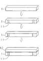
图1为本发明较佳实施例的步骤流程图。Fig. 1 is a flow chart of steps of a preferred embodiment of the present invention.
图2为本发明较佳实施例工艺的剖面示意图(一)。Fig. 2 is a schematic cross-sectional view (1) of the process of a preferred embodiment of the present invention.
图3为本发明较佳实施例工艺的剖面示意图(二)。Fig. 3 is a schematic cross-sectional view (2) of the process of a preferred embodiment of the present invention.
图4为本发明较佳实施例工艺的剖面示意图(三)。Fig. 4 is a schematic cross-sectional view (3) of the process of a preferred embodiment of the present invention.
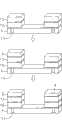
图5为本发明另一实施例的剖面图。Fig. 5 is a cross-sectional view of another embodiment of the present invention.
图6为本发明另一实施例的步骤流程图。FIG. 6 is a flow chart of steps in another embodiment of the present invention.
附图中主要元件符号说明:Explanation of main component symbols in the attached drawings:
1陶瓷基板,11贯穿孔,13导电金属层,12金属层,14防蚀刻金属层,2干膜,3无氧薄带,31挡墙,4防氧化焊接层。1 ceramic substrate, 11 through hole, 13 conductive metal layer, 12 metal layer, 14 anti-etching metal layer, 2 dry film, 3 oxygen-free thin strip, 31 retaining wall, 4 anti-oxidation welding layer.
具体实施方式Detailed ways
本发明的陶瓷基板表面镀上金属层及导电金属层,并进行曝光显影、蚀刻形成预设线路部份之后,可于导电金属层表面黏合有利用氧化铝、玻璃粉及可真空烧结黏稠剂所制成的无氧薄带,再进行无氧炉共烧成形为挡墙,即可避免导电金属层氧化让焊接、电镀工艺顺利作业,以此避免产生废品、瑕疵品,进而提升产品良率及降低生产成本。The surface of the ceramic substrate of the present invention is plated with a metal layer and a conductive metal layer, and after exposure, development, and etching to form a predetermined circuit part, the surface of the conductive metal layer can be bonded with aluminum oxide, glass powder and a viscous agent that can be vacuum sintered. The oxygen-free thin strip is then co-fired in an oxygen-free furnace to form a retaining wall, which can prevent the oxidation of the conductive metal layer and allow the welding and electroplating processes to operate smoothly, thereby avoiding waste and defective products, thereby improving product yield and reduce manufacturing cost.
为能够理解本发明上述目的及功效,以下结合附图并列举较佳实施例作详细说明。In order to understand the above purpose and effects of the present invention, preferred embodiments will be described in detail below in conjunction with the accompanying drawings.
请参阅图1、2、3、4所示,为本发明较佳实施例的步骤流程图、较佳实施例工艺的剖面示意图(一)、剖面示意图(二)、剖面示意图(三),由图中可以清楚看出,高精密度陶瓷基板工艺必须以电镀及高准度曝光/蚀刻方式制作,有别于一般以印刷方式制作的陶瓷基板,是利用氮化铝(AlN)或氧化铝(Al2O3)材质制成软生胚,且于软生胚上打孔,再进行烧结使软生胚成型为具一个或一个以上贯穿孔11的陶瓷基板1,再于陶瓷基板1表面以镀膜方式(coating)镀上金属层12,其金属层12可为镍、铬或镍铬硅与铜的合金(Ni/Cr/Si+Cu)、铁钴合金(Fe/Co)、铁钴镍合金(Fe/Co/Ni)等材质所制成,且金属层12的厚度可为0.15μm~0.5μm。Please refer to Fig. 1, 2, 3, and 4, which are a schematic sectional view (one), a schematic sectional view (two), and a schematic sectional view (three) of a step flow chart of a preferred embodiment of the present invention, a preferred embodiment process, by It can be clearly seen from the figure that the high-precision ceramic substrate process must be produced by electroplating and high-precision exposure/etching, which is different from the general ceramic substrate produced by printing, which uses aluminum nitride (AlN) or aluminum oxide ( Al2 O3 ) material is made into a soft green body, and holes are drilled on the soft green body, and then sintered so that the soft green body is formed into a
该金属层12表面贴附干膜2,干膜2进行光学微影技术的曝光显影处理后让预设线路处的干膜2去除,再于预设线路处未受干膜2遮挡的金属层12上方利用镀膜方式镀上导电金属层13,其导电金属层13为以铜材质所制成,且导电金属层13的厚度可为50μm~75μm,导电金属层13上则以镀膜方式镀上防蚀刻金属层14,其防蚀刻金属层14可为银、金等材质所制成,且防蚀刻金属层14的厚度可为0.01μm~0.1μm,再于去除干膜2后,对去除干膜2的金属层12进行蚀刻处理,让蚀刻液(如氯化铁、氯化铜等)去除金属层12,便可留下所需的线路,此时,若有残留防蚀刻金属层14,再以去除药剂把防蚀刻金属层14由导电金属层13上剥离。The surface of the
再于预定的导电金属层13上利用水压机黏合有无氧薄带3,其无氧薄带3为利用低温共烧陶瓷(Low Temperature Cofired Ceramics;LTCC)或氧化铝(Al2O3)与玻璃粉及黏稠剂依预定百分比作调浆、制带所制成,黏稠剂可为聚丙酮(Polyacetones)、低烷基丙烯酸酯共聚物(Copolymer of Lower Alkyl Acrylates)或甲基丙烯酸酯(Methacrylates)等符合可在真空状态下进行烧结的材质,所制成的生胚送入无氧炉进行共烧时,便可使无氧薄带3成形为挡墙31,并于导电金属层13表面镀上防氧化焊接层4,其防氧化焊接层4可为金、银或镍等金属,便完成本发明的工艺。Then, on the predetermined
请再参阅图1、2、3、4所示,为本发明较佳实施例的步骤流程图、较佳实施例工艺的剖面示意图(一)、剖面示意图(二)、剖面示意图(三),由图中可以清楚看出,本发明陶瓷基板1工艺的步骤流程为包括:Please refer again to Fig. 1, 2, 3, and 4, which are a flow chart of the steps of a preferred embodiment of the present invention, a schematic sectional view (one), a schematic sectional view (two), and a schematic sectional view (three) of the process of a preferred embodiment of the present invention, It can be clearly seen from the figure that the steps of the
(100)软生胚打孔。(100) soft raw embryo punching.
(101)软生胚烧结形成具一个或一个以上贯穿孔11的陶瓷基板1。(101) The soft green body is sintered to form a
(102)陶瓷基板1表面镀上金属层12。(102) The surface of the
(103)金属层12表面贴附干膜2。(103) Paste the
(104)对干膜2进行曝光显影,去除线路部份的干膜2。(104) Exposing and developing the
(105)于显露的线路部份金属层12表面依序镀上导电金属层13及防蚀刻金属层14。(105) Plating a
(106)去除干膜2。(106) Remove
(107)将去除干膜2的金属层12进行蚀刻。(107) Etching the
(108)导电金属层13表面黏合有利用氧化铝、玻璃粉及黏稠剂依预定百分比作调浆、制带所制成的无氧薄带3。(108) The surface of the
(109)送入无氧炉进行共烧并使无氧薄带3成形为挡墙31。(109) Sending into an oxygen-free furnace for co-firing and forming the oxygen-free
(110)在导电金属层13表面镀上防氧化焊接层4。(110) Plating an
上述陶瓷基板1表面镀上金属层12的方法,可为溅镀钛金属或利用纳米接口活性剂对陶瓷基板1进行表面改质,再镀上镍、铬、金、银等金属,且金属层12、导电金属层13、防蚀刻金属层14、防氧化焊接层4等工艺的镀膜方式可利用真空镀膜、化学蒸镀、溅镀或化学电镀等普遍且便宜的镀膜方式,然而有关镀上金属层12、导电金属层13、防蚀刻金属层14、防氧化焊接层4的方法为公知的技术,且该细部构成非本发明要点,兹不再赘述。The method for coating the
当完成上述步骤后,便可进行后续的设置电阻、电容或其它电子组件等工艺,由于在无氧炉共烧,使无氧薄带3烧结成形为硬胚时,其导电金属层13表面将不会接触到氧气,便可避免铜材质的导电金属层13氧化成为氧化铜,由于氧化铜将会在焊接、电镀工艺中导致较差的沾润,便会造成已镀上的金属层剥落及使焊接不沾,让后续工艺产生问题而成为废品、瑕疵品,因此本发明利用无氧炉共烧,即可避免上述问题产生,不仅可提升产品良率,更可大幅度降低生产成本。After the above steps are completed, the subsequent process of setting resistors, capacitors or other electronic components can be carried out. Due to the co-firing in the oxygen-free furnace, when the oxygen-free
该无氧薄带3烧结后将会成为挡墙31,如此一来,在相邻防氧化焊接层4进行打线、芯片倒装或焊接芯片后,便可利用挡墙31来挡止芯片所发出光源,让完成后续工艺的发光二极管可在发出光源后,利用挡墙3After the oxygen-free
1来限制光源照射方向,以此达到发出所需光型的光源的目的。1 to limit the irradiation direction of the light source, so as to achieve the purpose of emitting the light source of the required light type.
请再参阅图4、图5所示,为本发明工艺的剖面示意图(三)、另一实施例的剖面图,由图中可以清楚看出,陶瓷基板1除可在一侧表面镀上金属层12、导电金属层13、挡墙31、防氧化焊接层4等,亦可于陶瓷基板1二侧表面分别镀上金属层12、导电金属层13、挡墙31、防氧化焊接层4等,并通过贯穿孔11内镀上导电金属,让二侧结构相互导电,以此达到节省空间、缩小体积的目的。Please refer again to Fig. 4 and shown in Fig. 5, which are a schematic sectional view (three) of the process of the present invention and a sectional view of another embodiment, as can be clearly seen from the figure, the
另,请参阅图1、2、6所示,为本发明较佳实施例的步骤流程图、工艺的剖面示意图(一)、另一实施例的步骤流程图,由图中可以清楚看出,该陶瓷基板1工艺的步骤流程为包括:In addition, please refer to shown in Fig. 1, 2, 6, it is the flow chart of the steps of the preferred embodiment of the present invention, the schematic cross-sectional view of the process (1), the flow chart of the steps of another embodiment, as can be clearly seen from the figure, The step process of the
(200)软生胚烧结形成陶瓷基板1。(200) The soft green body is sintered to form the
(201)陶瓷基板1打孔形成一个或一个以上的贯穿孔11。(201) The
(202)陶瓷基板1表面镀上金属层12。(202) Coating the
(203)金属层12表面贴附干膜2。(203) Paste the
(204)对干膜2进行曝光显影,去除线路部份的干膜2。(204) Exposing and developing the
(205)于显露的线路部份金属层12表面依序镀上导电金属层13及防蚀刻金属层14。(205) Plating a
(206)去除干膜2。(206) Remove
(207)将去除干膜2的金属层12进行蚀刻。(207) Etching the
(208)导电金属层13表面黏合有利用氧化铝、玻璃粉及黏稠剂依预定百分比作调浆、制带所制成的无氧薄带3。(208) The surface of the
(209)送入无氧炉进行共烧并使无氧薄带3成形为挡墙31。(209) Sending into an oxygen-free furnace for co-firing and forming the oxygen-free
(210)在导电金属层13表面镀上防氧化焊接层4。(210) Plating an
由上述步骤可得知,该氮化铝(AlN)或氧化铝(Al2O3)材质制成的软生胚,可于烧结后再以激光方式打孔形成一个或一个以上的贯穿孔11,或先将软生胚打孔形成一个或一个以上的贯穿孔11后,再烧结,非因此即局限本发明的权利范围,如利用其它修饰及等效结构变化,均应同理包含于本发明的权利要求范围内。It can be known from the above steps that the soft green body made of aluminum nitride (AlN) or aluminum oxide (Al2 O3 ) can be drilled by laser after sintering to form one or more through
本发明为主要针对高精密度陶瓷基板工艺,而可在陶瓷基板1表面形成预设线路的金属层12、导电金属层13后,于导电金属层13表面黏合有无氧薄带3,其无氧薄带3为利用氧化铝、玻璃粉及在真空状态下进行烧结的黏稠剂依预定百分比作调浆、制带所制成,再送入无氧炉进行共烧,使无氧薄带3成形为挡墙31,便可避免铜材质的导电金属层13于共烧时氧化形成氧化铜,让后续的焊接、电镀工艺中不会产生废品、瑕疵品为主要保护重点,惟,以上所述仅为本发明的较佳实施例而已,非因此即局限本发明的权利范围,故举凡运用本发明说明书及附图内容所作的简易修饰及等效结构变化,均应同理包含于本发明的权利要求范围内。The present invention is mainly aimed at the high-precision ceramic substrate technology, and after forming the
Claims (13)
Translated fromChinesePriority Applications (1)
| Application Number | Priority Date | Filing Date | Title |
|---|---|---|---|
| CN2010101811848ACN102254831A (en) | 2010-05-20 | 2010-05-20 | High-precision ceramic substrate process |
Applications Claiming Priority (1)
| Application Number | Priority Date | Filing Date | Title |
|---|---|---|---|
| CN2010101811848ACN102254831A (en) | 2010-05-20 | 2010-05-20 | High-precision ceramic substrate process |
Publications (1)
| Publication Number | Publication Date |
|---|---|
| CN102254831Atrue CN102254831A (en) | 2011-11-23 |
Family
ID=44982002
Family Applications (1)
| Application Number | Title | Priority Date | Filing Date |
|---|---|---|---|
| CN2010101811848APendingCN102254831A (en) | 2010-05-20 | 2010-05-20 | High-precision ceramic substrate process |
Country Status (1)
| Country | Link |
|---|---|
| CN (1) | CN102254831A (en) |
Cited By (4)
| Publication number | Priority date | Publication date | Assignee | Title |
|---|---|---|---|---|
| CN106413270A (en)* | 2016-11-04 | 2017-02-15 | 大连大学 | Aluminum nitride ceramic circuit board and preparation method thereof |
| CN109152221A (en)* | 2018-09-06 | 2019-01-04 | 中国电子科技集团公司第三十八研究所 | The forming method of shallow-layer circuit shape cavity on a kind of low-temperature co-fired ceramic substrate |
| CN113263605A (en)* | 2015-06-29 | 2021-08-17 | 康宁股份有限公司 | Production line, method, and sintered product |
| US11577427B2 (en) | 2015-06-29 | 2023-02-14 | Corning Incorporated | Manufacturing system, process, article, and furnace |
- 2010
- 2010-05-20CNCN2010101811848Apatent/CN102254831A/enactivePending
Cited By (14)
| Publication number | Priority date | Publication date | Assignee | Title |
|---|---|---|---|---|
| US11768032B2 (en) | 2015-06-29 | 2023-09-26 | Corning Incorporated | Method of manufacturing ceramic tape |
| US12270604B2 (en) | 2015-06-29 | 2025-04-08 | Corning Incorporated | Manufacturing line, process, and sintered article |
| US12429281B2 (en) | 2015-06-29 | 2025-09-30 | Corning Incorporated | Manufacturing line, process, and sintered article |
| US11629915B2 (en) | 2015-06-29 | 2023-04-18 | Corning Incorporated | Method of manufacturing ceramic tape |
| CN113263605A (en)* | 2015-06-29 | 2021-08-17 | 康宁股份有限公司 | Production line, method, and sintered product |
| CN113263605B (en)* | 2015-06-29 | 2023-02-03 | 康宁股份有限公司 | Production line, method, and sintered product |
| US11745385B2 (en) | 2015-06-29 | 2023-09-05 | Corning Incorporated | Manufacturing system, process, article, and furnace |
| US11577427B2 (en) | 2015-06-29 | 2023-02-14 | Corning Incorporated | Manufacturing system, process, article, and furnace |
| US11953264B2 (en) | 2015-06-29 | 2024-04-09 | Corning Incorporated | Manufacturing line, process, and sintered article |
| US11919196B2 (en) | 2015-06-29 | 2024-03-05 | Corning Incorporated | Manufacturing system, process, article, and furnace |
| CN106413270A (en)* | 2016-11-04 | 2017-02-15 | 大连大学 | Aluminum nitride ceramic circuit board and preparation method thereof |
| CN106413270B (en)* | 2016-11-04 | 2019-04-05 | 大连大学 | A kind of aluminium nitride ceramics circuit board and preparation method |
| CN109152221A (en)* | 2018-09-06 | 2019-01-04 | 中国电子科技集团公司第三十八研究所 | The forming method of shallow-layer circuit shape cavity on a kind of low-temperature co-fired ceramic substrate |
| CN109152221B (en)* | 2018-09-06 | 2020-08-11 | 中国电子科技集团公司第三十八研究所 | A method for forming a shallow loop-shaped cavity on a low-temperature co-fired ceramic substrate |
Similar Documents
| Publication | Publication Date | Title |
|---|---|---|
| JP2011109057A (en) | Process of manufacturing high-accuracy ceramic substrate | |
| US9504165B2 (en) | Method of forming conductive traces on insulated substrate | |
| CN103533765A (en) | Method for improving metal surface roughness on ceramic through hole substrate and ceramic substrate | |
| CN107004752B (en) | Substrate for light-emitting device, light-emitting device, and lighting device | |
| CN102709439A (en) | LED ceramic bracket and preparation method thereof | |
| CN104812166B (en) | A kind of reflective heat conduction metal-based pcb board manufacture method | |
| CN102254831A (en) | High-precision ceramic substrate process | |
| CN102024883B (en) | Manufacturing method of light-emitting diode heat dissipation substrate | |
| US9397279B2 (en) | Electric conductive heat dissipation substrate | |
| CN112490131A (en) | Lead frame preparation method based on etching process | |
| CN108184312A (en) | A kind of double-side conduction ceramic circuit-board and preparation method thereof | |
| CN111430247A (en) | L TCC (cross-resistance coefficient) device manufactured based on titanium substrate electroplating pattern transfer method | |
| JP2011109056A (en) | Method of manufacturing ceramic substrate | |
| CN202662663U (en) | LED ceramic bracket | |
| WO2018170958A1 (en) | Double-sided aluminum-based circuit board and fabrication method therefor | |
| JP2015195309A (en) | Manufacturing method of metal-ceramics circuit board | |
| TWI406603B (en) | High thermal conductivity substrate process | |
| TW201542078A (en) | Method for manufacturing ceramic substrate heat-dissipating structure | |
| CN101883473A (en) | Double-sided electrical conduction composite board and manufacturing method thereof | |
| CN110402030A (en) | A method for manufacturing a heat dissipation structure of a printed circuit board and a printed circuit board | |
| TWI636716B (en) | Process to produce multiple plane metalization on a ceramic substrate | |
| TWI442847B (en) | Method for manufacturing three - dimensional circuit of ceramic substrate | |
| CN113275567B (en) | A kind of laser sintering molding method | |
| CN102034905B (en) | Light-emitting diode heat dissipation substrate and manufacturing method thereof | |
| CN212786044U (en) | High-reliability rivet-shaped electroplating hole structure of circuit board |
Legal Events
| Date | Code | Title | Description |
|---|---|---|---|
| C06 | Publication | ||
| PB01 | Publication | ||
| C10 | Entry into substantive examination | ||
| SE01 | Entry into force of request for substantive examination | ||
| C02 | Deemed withdrawal of patent application after publication (patent law 2001) | ||
| WD01 | Invention patent application deemed withdrawn after publication | Application publication date:20111123 |