CN102253752B - Touch panel and touch display panel - Google Patents
Touch panel and touch display panelDownload PDFInfo
- Publication number
- CN102253752B CN102253752BCN2011102169542ACN201110216954ACN102253752BCN 102253752 BCN102253752 BCN 102253752BCN 2011102169542 ACN2011102169542 ACN 2011102169542ACN 201110216954 ACN201110216954 ACN 201110216954ACN 102253752 BCN102253752 BCN 102253752B
- Authority
- CN
- China
- Prior art keywords
- sensing
- electrode
- series
- touch
- electrode series
- Prior art date
- Legal status (The legal status is an assumption and is not a legal conclusion. Google has not performed a legal analysis and makes no representation as to the accuracy of the status listed.)
- Active
Links
Images


Classifications
- G—PHYSICS
- G06—COMPUTING OR CALCULATING; COUNTING
- G06F—ELECTRIC DIGITAL DATA PROCESSING
- G06F3/00—Input arrangements for transferring data to be processed into a form capable of being handled by the computer; Output arrangements for transferring data from processing unit to output unit, e.g. interface arrangements
- G06F3/01—Input arrangements or combined input and output arrangements for interaction between user and computer
- G06F3/03—Arrangements for converting the position or the displacement of a member into a coded form
- G06F3/041—Digitisers, e.g. for touch screens or touch pads, characterised by the transducing means
- G06F3/044—Digitisers, e.g. for touch screens or touch pads, characterised by the transducing means by capacitive means
- G06F3/0443—Digitisers, e.g. for touch screens or touch pads, characterised by the transducing means by capacitive means using a single layer of sensing electrodes
- G—PHYSICS
- G06—COMPUTING OR CALCULATING; COUNTING
- G06F—ELECTRIC DIGITAL DATA PROCESSING
- G06F3/00—Input arrangements for transferring data to be processed into a form capable of being handled by the computer; Output arrangements for transferring data from processing unit to output unit, e.g. interface arrangements
- G06F3/01—Input arrangements or combined input and output arrangements for interaction between user and computer
- G06F3/03—Arrangements for converting the position or the displacement of a member into a coded form
- G06F3/041—Digitisers, e.g. for touch screens or touch pads, characterised by the transducing means
- G06F3/044—Digitisers, e.g. for touch screens or touch pads, characterised by the transducing means by capacitive means
- G06F3/0446—Digitisers, e.g. for touch screens or touch pads, characterised by the transducing means by capacitive means using a grid-like structure of electrodes in at least two directions, e.g. using row and column electrodes
Landscapes
- Engineering & Computer Science (AREA)
- General Engineering & Computer Science (AREA)
- Theoretical Computer Science (AREA)
- Human Computer Interaction (AREA)
- Physics & Mathematics (AREA)
- General Physics & Mathematics (AREA)
- Position Input By Displaying (AREA)
Abstract
Translated fromChinese
Description
Translated fromChinese技术领域technical field
本发明是有关一种触摸面板及触摸显示面板(touch sensing displaypanel),且特别是有关一种电容式触摸显示面板(capacitive touch sensingdisplay panel)。The present invention relates to a touch panel and a touch sensing display panel, and in particular to a capacitive touch sensing display panel.
背景技术Background technique
近年来,随着资讯技术、无线行动通讯和资讯家电等各项应用的快速发展,为了达到更便利、体积更轻巧化以及更人性化的目的,触摸面板已经逐渐取代键盘与滑鼠,成为许多资讯产品的主要输入装置。一般而言,触摸面板大致可区分为电阻式触摸面板、电容式触摸面板、光学式触摸面板、声波式触摸面板、电磁式触摸面板等。以电容式触摸面板为例,根据其驱动与感应方式可分为自电容型(self capacitive)触摸面板以及互电容型(mutual capacitive)触摸面板两大类。In recent years, with the rapid development of various applications such as information technology, wireless mobile communication, and information home appliances, in order to achieve more convenience, smaller volume, and more humanization, touch panels have gradually replaced keyboards and mice, and have become many The primary input device for information products. Generally speaking, touch panels can be roughly classified into resistive touch panels, capacitive touch panels, optical touch panels, acoustic wave touch panels, electromagnetic touch panels, and the like. Taking the capacitive touch panel as an example, according to its driving and sensing methods, it can be divided into two categories: self capacitive touch panel and mutual capacitive touch panel.
公知的互电容型触摸面板包括多个沿着X轴方向延伸的第一电极串列,以及多个沿着Y轴方向延伸的第二电极串列,且X轴方向与Y轴方向不同。当使用者以手指触碰触摸面板时,会改变第一电极串列与第二电极串列之间的电容,将此改变信号传回控制器,即可计算出触摸位置的座标。当其与显示面板结合构成互电容型触摸显示面板时,显示面板可以根据使用者所为的触摸位置的选择而进行显示画面的改变。A known mutual capacitance touch panel includes a plurality of first electrode series extending along the X-axis direction and a plurality of second electrode series extending along the Y-axis direction, and the X-axis direction is different from the Y-axis direction. When the user touches the touch panel with a finger, the capacitance between the first electrode series and the second electrode series will be changed, and the change signal will be sent back to the controller to calculate the coordinates of the touch position. When it is combined with the display panel to form a mutual capacitive touch display panel, the display panel can change the display screen according to the user's selection of the touch position.
一般来说,为了提高触摸面板的感应灵敏度,必须增加第一电极串列与第二电极串列之间之间距,藉此增大第一电极串列与第二电极串列之间的电容变化量来增强电容改变的感应信号。然而,增大第一电极串列与第二电极串列之间之间距虽然可以增强使用者触碰点的感应信号,但当第一电极串列与第二电极串列之间之间距过大时,由于相邻感应信号之间的重叠区域不足,无法利用相邻感应信号的重叠比例搭配内插法准确地计算出触摸点,导致公知触摸面板无法清楚地判别出使用者的触碰轨迹。具体而言,当使用者以手指在触摸面板上画直线时,由于相邻感应信号彼此的重叠区域不足,将导致触摸面板的感应线性度(linearity)不佳的问题。Generally speaking, in order to improve the sensing sensitivity of the touch panel, the distance between the first electrode series and the second electrode series must be increased, thereby increasing the capacitance change between the first electrode series and the second electrode series The amount to enhance the sensing signal of capacitance change. However, although increasing the distance between the first electrode series and the second electrode series can enhance the sensing signal of the user's touch point, when the distance between the first electrode series and the second electrode series is too large At this time, due to the insufficient overlapping area between adjacent sensing signals, the touch point cannot be accurately calculated by using the overlapping ratio of adjacent sensing signals with the interpolation method, so that the known touch panel cannot clearly distinguish the user's touch track. Specifically, when the user draws a straight line on the touch panel with a finger, the overlapping area of adjacent sensing signals is insufficient, which will lead to a problem of poor sensing linearity of the touch panel.
发明内容Contents of the invention
本发明提供一种触摸面板以及触摸显示面板,其具有较佳的感应线性度。The invention provides a touch panel and a touch display panel, which have better sensing linearity.
本发明提出一种触摸面板,其包括一基板、多条驱动电极串列以及多条感应电极串列。驱动电极串列与感应电极串列配置于基板上,其中驱动电极串列分别沿第一方向延伸,感应电极串列分别沿第二方向延伸,且第一方向与第二方向不同。驱动电极串列与感应电极串列彼此交错以构成多个感应单元,其中各感应单元具有一中间区域以及一外围区域,位于中间区域的驱动电极串列与感应电极串列之间具有一第一电极间距,位于外围区域的驱动电极串列与感应电极串列之间具有一第二电极间距,且第二电极间距小于第一电极间距。所述驱动电极串列与所述感应电极串列交错构成感应单元,感应单元具有一几何中心。在各该感应单元中,该几何中心到边界的距离为D,该中间区域的边界到该几何中心的距离d满足关系式:0≤d≤0.95D。该中间区域的边界到该几何中心的距离d满足关系式:0≤d≤0.8D。该中间区域的边界到该几何中心的距离d满足关系式:0≤d≤0.5D。在各该感应单元中,该第二电极间距G2与该第一电极间距G1的比值范围为0.06≤G2/G1≤0.8。该第二电极间距G2与该第一电极间距G1的比值范围为0.07≤G2/G1≤0.7。该第二电极间距G2与该第一电极间距G1的比值范围为0.1≤G2/G1≤0.6。所述驱动电极串列彼此电性绝缘,且所述感应电极串列彼此电性绝缘。各该驱动电极串列包括一沿着第一方向延伸的驱动电极主干以及多条沿着第二方向延伸的驱动电极分支,而各该感应电极串列包括一沿着第二方向延伸的感应电极主干以及多条沿着第一方向延伸的感应电极分支。所述各该驱动电极主干包括多个条状导体以及多个驱动桥接线,各该驱动桥接线跨越对应的各该感应电极主干并连接于二相邻的条状导体之间。进一步包含多个介电图案层,分别位于所述驱动电极串列与所述感应电极串列的交错点上,其特征在于:各该介电图案层介于各该驱动电极串列以及各该感应电极串列之间,以电性隔离该驱动电极与该感应电极。The invention provides a touch panel, which includes a substrate, a plurality of driving electrode series and a plurality of sensing electrode series. The driving electrode series and the sensing electrode series are disposed on the substrate, wherein the driving electrode series respectively extend along a first direction, and the sensing electrode series respectively extend along a second direction, and the first direction is different from the second direction. The driving electrode series and the sensing electrode series are interlaced to form a plurality of sensing units, wherein each sensing unit has a middle area and a peripheral area, and a first first electrode is located between the driving electrode series and the sensing electrode series in the middle area. The electrode spacing, there is a second electrode spacing between the driving electrode series and the sensing electrode series in the peripheral area, and the second electrode spacing is smaller than the first electrode spacing. The driving electrode series and the sensing electrode series are interlaced to form a sensing unit, and the sensing unit has a geometric center. In each sensing unit, the distance from the geometric center to the boundary is D, and the distance d from the boundary of the middle area to the geometric center satisfies the relationship: 0≤d≤0.95D. The distance d from the boundary of the middle area to the geometric center satisfies the relational expression: 0≤d≤0.8D. The distance d from the boundary of the middle area to the geometric center satisfies the relational expression: 0≤d≤0.5D. In each sensing unit, the ratio of the second electrode spacing G2 to the first electrode spacing G1 ranges from 0.06≦G2/G1≦0.8. The range of the ratio of the second electrode gap G2 to the first electrode gap G1 is 0.07≦G2/G1≦0.7. The range of the ratio of the second electrode gap G2 to the first electrode gap G1 is 0.1≦G2/G1≦0.6. The driving electrode series are electrically insulated from each other, and the sensing electrode series are electrically insulated from each other. Each of the driving electrode series includes a driving electrode trunk extending along the first direction and a plurality of driving electrode branches extending along the second direction, and each of the sensing electrode series includes a sensing electrode extending along the second direction The trunk and a plurality of sensing electrode branches extending along the first direction. Each of the driving electrode trunks includes a plurality of strip conductors and a plurality of driving bridge lines, and each of the driving bridge lines spans the corresponding sensing electrode trunks and is connected between two adjacent strip conductors. It further includes a plurality of dielectric pattern layers, which are respectively located at the intersection points of the driving electrode series and the sensing electrode series, and is characterized in that: each of the dielectric pattern layers is interposed between each of the driving electrode series and each of the The sensing electrode series are electrically isolated from the driving electrodes and the sensing electrodes.
本发明另提出一种触摸显示面板,其包括一显示面板以及一触摸感应元件。触摸感应元件配置于显示面板上,且触摸感应元件包括多条驱动电极串列以及多条感应电极串列。驱动电极串列分别沿第一方向延伸,感应电极串列分别沿第二方向延伸,驱动电极串列与感应电极串列彼此交错以构成多个感应单元,其中各感应单元具有一中间区域以及一外围区域,位于中间区域的驱动电极串列与感应电极串列之间具有一第一电极间距,位于外围区域的驱动电极串列与感应电极串列之间具有一第二电极间距,且第二电极间距小于第一电极间距。该触摸感应元件直接整合于该显示面板上。该触摸感应元件透过该辅助基板而配置于该显示面板上。该触摸感应元件嵌入整合于该显示面板内。The present invention further provides a touch display panel, which includes a display panel and a touch sensing element. The touch sensing element is configured on the display panel, and the touch sensing element includes a plurality of driving electrode series and a plurality of sensing electrode series. The driving electrode series extend along the first direction, the sensing electrode series respectively extend along the second direction, the driving electrode series and the sensing electrode series are interlaced to form a plurality of sensing units, wherein each sensing unit has a middle area and a In the peripheral area, there is a first electrode spacing between the driving electrode series and the sensing electrode series in the middle area, and there is a second electrode spacing between the driving electrode series and the sensing electrode series in the peripheral area, and the second The electrode pitch is smaller than the first electrode pitch. The touch sensing element is directly integrated on the display panel. The touch sensing element is configured on the display panel through the auxiliary substrate. The touch sensing element is embedded and integrated in the display panel.
基于上述,本发明的触摸面板以及触摸显示面板中将感应单元划分为不同的区域,且分别在感应单元的不同区域中,使驱动电极串列与感应串列之间的电极间距满足特定关系,藉此,能提高整体的感应灵敏度,并可以改善电容触摸式面板的线性度。Based on the above, in the touch panel and the touch display panel of the present invention, the sensing unit is divided into different areas, and in different areas of the sensing unit, the electrode spacing between the driving electrode series and the sensing series satisfies a specific relationship, Thereby, the overall sensing sensitivity can be improved, and the linearity of the capacitive touch panel can be improved.
为让本发明的上述特征和优点能更明显易懂,下文特举实施例,并配合所附图式作详细说明如下。In order to make the above-mentioned features and advantages of the present invention more comprehensible, the following specific embodiments are described in detail together with the accompanying drawings.
附图说明Description of drawings
图1A与图1C为本发明一实施例中不同的触摸显示面板的示意图。FIG. 1A and FIG. 1C are schematic diagrams of different touch display panels according to an embodiment of the present invention.
图2为本发明一实施例中一种触摸面板的上视图。Fig. 2 is a top view of a touch panel in an embodiment of the present invention.
图3A为图2的触摸面板中一个感应单元的放大示意图。FIG. 3A is an enlarged schematic diagram of a sensing unit in the touch panel of FIG. 2 .
图3B为图3A沿A-A’剖面线的剖面示意图。Fig. 3B is a schematic cross-sectional view of Fig. 3A along the section line A-A'.
图4A为图2的触摸面板中局部区域的放大示意图。FIG. 4A is an enlarged schematic view of a local area of the touch panel in FIG. 2 .
图4B为图4A的感应信号的能量分布示意图。FIG. 4B is a schematic diagram of the energy distribution of the sensing signal in FIG. 4A .
图5A为一种作为比较例的触摸面板的结构示意图。FIG. 5A is a schematic structural diagram of a touch panel as a comparative example.
图5B为图5A的感应信号的能量分布示意图。FIG. 5B is a schematic diagram of the energy distribution of the sensing signal in FIG. 5A .
图6A与图6B绘示图4A与图5A的触摸面板的感应圆性度以及感应线性度的比较图。FIG. 6A and FIG. 6B are diagrams comparing the sensing circularity and sensing linearity of the touch panels in FIG. 4A and FIG. 5A .
【附图标记说明】[Description of Reference Signs]


具体实施方式Detailed ways
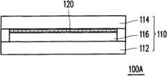
图1A至图1C为本发明一实施例中不同的触摸显示面板的示意图。请先参照图1A,本实施例的触摸显示面板100A包括一显示面板110以及一配置于显示面板110的触摸感应元件120。在本实施例中,触摸感应元件120可内建于显示面板110中,其中显示面板110可以是液晶显示面板、有机发光显示面板(Organic light emitting display panel)、电泳显示面板(Electrophoreticdisplay panel)或是电浆显示面板(Plasma display panel),本发明并不限定显示面板110的种类。本实施例的显示面板110以液晶显示面板为例,其包括一主动元件阵列基板112、一彩色滤光片基板114以及一位于上述二基板112、114之间的液晶层116,而触摸感应元件120可嵌入整合于彩色滤光片基板114的内表面上。换言的,触摸感应元件120位于彩色滤光片基板114以及液晶层116之间,因此本实施例的触摸显示面板100A即所谓的内建式设计(In-cell design)。1A to 1C are schematic diagrams of different touch display panels according to an embodiment of the present invention. Please refer to FIG. 1A , the
此外,触摸感应元件120亦可以直接形成于显示面板100B的彩色滤光片基板114的外表面上,如图1B所示,因此本实施例的触摸显示面板100B即所谓的整合式设计(On-cell design)。当然,如图1C所示,触摸感应元件120亦可以先制作于一辅助基板130上,再将已形成有触摸感应元件120的辅助基板130贴附于彩色滤光片基板114的外表面上,因此本实施例的触摸显示面板100C即所谓的外贴式设计(Out-cell design)。In addition, the
值得注意是,图1C中的辅助基板130以及触摸感应元件120即构成本实施例的触摸面板200,其与显示面板110结合即构成本实施例的触摸显示面板100C。换言的,本发明的触摸感应元件120可整合于显示面板110中(可如图1A直接内建于的彩色滤光片基板114的内表面上,或是如图1B直接形成于彩色滤光片基板114的外表面上),亦可藉由辅助基板130来与显示面板110结合,本发明并不限定触摸感应元件120与显示面板110的结合方式。It is worth noting that the
以下将针对触摸面板以及触摸显示面板上的不同型态的触摸感应元件详细说明。Different types of touch sensing elements on the touch panel and the touch display panel will be described in detail below.
图2为本发明一实施例中一种触摸面板的上视图。请参照图2,本实施例的触摸面板200包括一基板210、多条驱动电极串列(series)220以及多条感应电极串列230,其中基板210可以是如前述绘示于图1A至图1C的辅助基板130或是彩色滤光片基板114。如图2所示,驱动电极串列220配置于基板210上并彼此电性绝缘,且驱动电极串列220分别沿第一方向D1延伸。感应电极串列230配置于基板210上并彼此电性绝缘,且感应电极串列230分别沿第二方向D2延伸,且第一方向D1与第二方向D2不同,在本实施例中,第一方向D1与第二方向D2实质上垂直。Fig. 2 is a top view of a touch panel in an embodiment of the present invention. Referring to FIG. 2, the
请参照图2,驱动电极串列220与感应电极串列230彼此交错以构成多个感应单元240,在图2中仅例示性地绘示出3×5阵列的感应单元240。如图2所示,各感应单元240具有一中间区域240C以及一外围区域240S,其中中间区域240C例如是图中以虚线框F所围出的范围,而外围区域240S例如是图中感应单元240边缘与虚线框F之间所围出的范围。特别的是,位于中间区域240C的驱动电极串列220与感应电极串列230之间具有一第一电极间距G1,位于外围区域240S的驱动电极串列220与感应电极串列230之间具有一第二电极间距G2,且第二电极间距G2小于第一电极间距G1。由于在各感应单元240中,位于外围区域240S的第二电极间距G2小于位于中间区域240C的第一电极间距G1,因此相邻感应单元240的感应信号可以较充分地重叠,当手指、触摸笔或其他物体在触摸面板200上画直线时,透过相邻感应信号所重叠的比例,可以利用内插法计算出触摸点,因而具有较佳的感应线性度,下文将详细说明。Please refer to FIG. 2 , the driving
为清楚说明本发明的触摸感应元件的结构,以下将以图3A辅助说明。In order to clearly illustrate the structure of the touch-sensing element of the present invention, FIG. 3A will be assisted in the following description.
图3A为图2的触摸面板中一个感应单元的放大示意图。请同时参照图2与图3A,驱动电极串列220与感应电极串列230彼此交错以在基板210上定义出多个阵列排列的感应单元240,在本实施例中,每一感应单元240对应至少一条驱动电极串列220以及至少一条感应电极串列230,且驱动电极串列220与感应电极串列230交错构成感应单元240。当手指、触摸笔或其他物体触摸到该感应单元240时,会改变该驱动电极串列220以及该感应电极串列230之间所耦合的电容,将此改变电容转为反应信号传回控制器,即可计算出触摸位置的座标。FIG. 3A is an enlarged schematic diagram of a sensing unit in the touch panel of FIG. 2 . Please refer to FIG. 2 and FIG. 3A at the same time. The driving
如图3A所示,本实施例的各驱动电极串列220包括沿着第一方向D1延伸的驱动电极主干220T以及多条沿着第二方向D2延伸的驱动电极分支220B,在本实施例中,第一方向D1例如为X方向,而第二方向D2例如为Y方向。相邻驱动电极串列220的驱动电极分支220B彼此相对,且具有一第一间隙S1,以确保驱动电极串列220之间彼此电性绝缘。本实施例的感应电极串列230包括多条沿着第二方向D2延伸的感应电极主干230T以及多条沿着第一方向D1延伸的感应电极分支230B,相邻感应电极串列230的感应电极分支230B彼此相对,且具有一第二间隙S2,以确保感应电极串列230之间彼此电性绝缘。值得一提的是,第一间隙S1与第二间隙S2的尺寸微小,不容易被使用者所察觉,因而使触摸面板200具有较佳的视觉效果。此外,为了使触摸面板200上各区域的透光度均匀并具有较佳的视觉效果,本实施例的各驱动电极主干220T、各驱动电极分支220B、各感应电极主干230T以及各感应电极分支230B可以分别由网状线或是孔线所构成,但本发明并不限定电极形状。As shown in FIG. 3A , each driving
如图3A的放大图所示,本实施例的驱动电极主干220T进一步包括多个沿第一方向D1延伸的条状导体222以及多个沿第一方向D1延伸的驱动桥接线224,其中各驱动桥接线224跨越对应的各感应电极主干230T并连接于二相邻的条状导体222之间。在本实施例中,条状导体222、感应电极主干230T以及感应电极分支230B的材质例如可以是相同。换言的,在本实施例中,条状导体222、感应电极主干230T以及感应电极分支230B属于同一层图案化薄膜,举例来说,条状导体222、感应电极主干230T以及感应电极分支230B的材质可皆为透明导电材料,如铟锡氧化物(ITO)、铟锌氧化物(IZO)等。此外,驱动桥接线224例如为有别于条状导体222、感应电极主干230T以及感应电极分支230B的膜层,其材质可以是金属,例如是铝、铜、银、金、钛、钼、铬、钨等以及其合金与迭层,。在变化实施例中,条状导体222、感应电极主干230T、感应电极分支230B以及驱动桥接线224的材质亦可均为金属,例如是铝、铜、银、金、钛、钼、铬、钨等以及其合金与迭层,此时线宽必须较小,较佳是小于10微米,以减少视觉可见度。As shown in the enlarged view of FIG. 3A , the driving
图3B为图3A的A-A’剖面的示意图。请参照图3B,为了有效地避免驱动电极串列220与感应电极串列230发生短路的情况,本实施例的触摸感应元件120可进一步包括多个介电图案层250,其中介电图案层250分别位于其中一条驱动桥接线224驱动下方,以确保每一驱动桥接线224驱动与感应电极串列230电性绝缘。Fig. 3B is a schematic diagram of the section A-A' of Fig. 3A. Please refer to FIG. 3B , in order to effectively avoid the short circuit between the driving
为清楚说明前述触摸感应元件在被触碰时的感应信号,以下将以绘示于前述图2A的触摸面板200为例,说明当使用者触碰前述感应单元240时,触摸面板200的感应线性度。In order to clearly illustrate the sensing signal of the aforementioned touch sensing element when it is touched, the following will take the
图4A为图2的触摸面板中局部区域放大示意图,而图4B为图4A的感应信号的能量分布示意图,其中图4A中示意性地绘示了使用者在触摸面板200上画直线的轨迹L,而图4B则对应为图4A的感应信号的能量分布示意图。请参照图4A,当令驱动电极串列220以及感应电极串列230的交错点(如图4A中的C点)为一感应单元240的几何中心C时,可以在触摸面板200上定义出多个阵列排列且重复的感应单元240。并且,如前述,各感应单元240被划分为中间区域240C(虚线框F所围出的范围)以及环绕中间区域240C的外围区域240S(感应单元240边缘与虚线框F所围出的范围)。具体而言,中间区域240C的范围可依照下述的关系进行设计:令感应单元240的几何中心C到边界的单元距离为D,且中间区域240C的边界到几何中心C的中心距离为d。其中,中心距离d与单元距离D的比值较佳地满足关系式:0≤d≤0.95D,更佳地是满足关系式0≤d≤0.8D,更佳地是满足关系式:0≤d≤0.5D。4A is an enlarged schematic diagram of a local area in the touch panel of FIG. 2, and FIG. 4B is a schematic diagram of the energy distribution of the sensing signal in FIG. 4A, wherein FIG. , and FIG. 4B is a schematic diagram corresponding to the energy distribution of the induction signal in FIG. 4A . Please refer to FIG. 4A , when the intersection point of the driving
举例而言,以本实施例的矩形的感应单元240为例,当以驱动电极串列220与感应电极串列230的交错几何中心作为XY座标轴的原点C(0,0)时,如左上方的感应单元240a,感应单元240a为-D≤x≤D且-D≤y≤D所围出的范围,中间区域240C例如为-0.95D≤x≤0.95D且-0.95D≤y≤0.95D所围出的范围,此时外围区域240S对应为-D≤x≤-0.95D,0.95D≤x≤D且-D≤y≤-0.95D,0.95D≤y≤D所围出的范围;另一方面,当感应单元240a的中间区域240C为-0.8D≤x≤0.8D且-0.8D≤y≤0.8D所围出的范围时,外围区域240S则对应为-D≤x≤-0.8D,0.8D≤x≤D且-D≤y≤-0.8D,0.8D≤y≤D所围出的范围;另一方面,当感应单元240a的中间区域240C为-0.5D≤x≤0.5D且-0.5D≤y≤0.5D所围出的范围时,外围区域240S则对应为-D≤x≤-0.5D,0.5D≤x≤D且-D≤y≤-0.5D,0.5D≤y≤D所围出的范围。For example, taking the rectangular sensing unit 240 of this embodiment as an example, when the intersection geometric center of the driving electrode series 220 and the sensing electrode series 230 is used as the origin C (0, 0) of the XY coordinate axis, as The upper left sensing unit 240a, the sensing unit 240a is a range surrounded by -D≤x≤D and -D≤y≤D, and the middle area 240C is, for example, -0.95D≤x≤0.95D and -0.95D≤y≤ The range enclosed by 0.95D, at this time, the peripheral area 240S corresponds to the area enclosed by -D≤x≤-0.95D, 0.95D≤x≤D and -D≤y≤-0.95D, 0.95D≤y≤D range; on the other hand, when the middle region 240C of the sensing unit 240a is the range enclosed by -0.8D≤x≤0.8D and -0.8D≤y≤0.8D, the peripheral region 240S corresponds to -D≤x≤ -0.8D, 0.8D≤x≤D and -D≤y≤-0.8D, 0.8D≤y≤D enclosed range; on the other hand, when the middle area 240C of the sensing unit 240a is -0.5D≤x ≤0.5D and -0.5D≤y≤0.5D, the peripheral area 240S corresponds to -D≤x≤-0.5D, 0.5D≤x≤D and -D≤y≤-0.5D, The range surrounded by 0.5D≤y≤D.
值得注意的是,感应单元的形状除了本实施例的矩形外,亦可以是圆形、菱形、三角形、六角形等,可依照设计需求改变,简言的,当感应单元的形状为圆形时,驱动电极串列与感应电极串列的交错几何中心是位于圆形的感应单元的圆心上,且中间区域的范围可依照前述的关系进行设计:中间区域的边界到几何中心的距离d较佳地满足关系式:0≤d≤0.95D,更佳地是满足关系式0≤d≤0.8D,更佳地是满足关系式:0≤d≤0.5D。It is worth noting that the shape of the sensing unit can be round, rhombus, triangle, hexagon, etc. in addition to the rectangle in this embodiment, which can be changed according to the design requirements. In short, when the shape of the sensing unit is circular , the interlaced geometric center of the driving electrode series and the sensing electrode series is located on the center of the circular sensing unit, and the range of the middle area can be designed according to the aforementioned relationship: the distance d from the boundary of the middle area to the geometric center is better Satisfy the relational expression: 0≤d≤0.95D, more preferably satisfy the relational expression 0≤d≤0.8D, more preferably satisfy the relational expression: 0≤d≤0.5D.
此时D则定义为圆形的感应单元的几何中心到边界的半径,易言的,本发明并不限定感应单元240的形状。In this case, D is defined as the radius from the geometric center to the boundary of the circular sensing unit. In other words, the present invention does not limit the shape of the
特别的是,在本实施例的各感应单元240中,位于外围区域240S的第二电极间距G2小于位于中间区域240C的第一电极间距G1。具体来说,第一电极间距G1与第二电极间距G2为驱动电极串列220以及感应电极串列230沿着第一方向D1或是第二方向D2的平行间距,图4A显示驱动电极串列220以及感应电极串列230沿着第二方向D2(Y方向)的平行间距。第二电极间距G2与第一电极间距G1的比值小于1,且第二电极间距G2与第一电极间距G1的比值满足关系式:0.06≤G2/G1≤0.8。更详细而言,第一电极间距G1与第二电极间距G2之间较佳地是满足关系式:0.07≤G2/G1≤0.7,更佳地是满足关系式:0.1≤G2/G1≤0.6。在本实施例中,第一电极间距G1与第二电极间距G2为驱动电极分支220B与相对的感应电极主干230T之间的距离,当然,在其他实施例中,第一电极间距G1与第二电极间距G2亦可为感应电极分支230B与相邻驱动电极主干220T之间的距离,本发明并不以此为限。In particular, in each
请同时参照图4A与图4B,当手指、触摸笔或其他物体沿着如图4A的触碰轨迹L依序触碰感应单元240p、感应单元240q、感应单元240r时,感应单元240p、感应单元240q、感应单元240r将分别产生对应的感应信号260p、感应信号260q、感应信号260r。如图4B所示,由于感应信号260p与感应信号260r在感应信号260q的波形范围内具有相当程度的重叠区域B,因此当使用者在碰触感应单元240q时,依据感应信号260p与感应信号260r的重叠比例可以精确地计算出触碰点相对于感应单元240q中心的方位。举例来说,请同时参照图4A与图4B,当触碰点为感应单元240q的中心C偏左的X1点时,感应信号260p会大于感应信号260r;而当触碰点为感应单元240q的中心偏右的X2点时,感应信号260p会小于感应信号260r,由于感应信号260p与感应信号260r之间成一定的比例关系,因此可以藉由内插法精确地计算出触碰点的位置。换言的,本发明的触摸面板可藉由缩小外围区域240S上的第二电极间距G2,来缩短两相邻中间区域240C之间的距离,藉此可以使相邻感应单元240p、240q、240r所产生的感应信号260p、260q、260r的重叠区域B增加,即可利用内插法精确地计算出触摸点,因而使本发明的触摸面板具有较佳的感应线性度。Please refer to FIG. 4A and FIG. 4B at the same time. When a finger, a touch pen or other objects sequentially touch the
此外,基于进一步提升感应灵敏度的考量,设计者进一步增加中间区域240C的第一电极间距G1,来增加驱动电极串列220以及感应电极串列230之间的电容变化量,藉此可以在维持感应线性度的前提下,进一步增强中间区域240C上电容改变的感应信号260,以提升感应单元240的感应灵敏度。In addition, based on the consideration of further improving the sensing sensitivity, the designer further increases the first electrode spacing G1 in the
相对于此,图5A与图5B绘示比较例的一种触摸面板。In contrast, FIG. 5A and FIG. 5B illustrate a touch panel of a comparative example.
图5A为比较例的一种触摸面板的示意图,而图5B为图5A的感应信号的能量分布示意图,其中图5A的触摸面板300中的驱动电极串列320与感应电极串列330分别等距地排列。如图5B所示,由于驱动电极串列320以及感应电极串列330之间的电极间距在感应单元340的各区域中为固定值,并没有改变电极间距,因此当使用者当手指、触摸笔或其他物体沿着如图5A的触碰轨迹依序触碰感应单元340p、感应单元340q、感应单元340r上画直线时,感应单元340p、感应单元340q与感应单元340r分别产生对应的感应信号360p、感应信号360q与感应信号360r,但因相邻的感应信号360p、感应信号360q、感应信号360r之间的重叠区域B不足,将无法利用相邻感应信号的重叠比例搭配内插法计算出触摸点,导致触摸面板300无法清楚地判别出使用者的触碰轨迹。5A is a schematic diagram of a touch panel of a comparative example, and FIG. 5B is a schematic diagram of the energy distribution of the sensing signal in FIG. 5A , wherein the
图6A与图6B进一步绘示图4A实施例与图5A比较例的触摸面板的感应线性度与感应圆性度的比较图,其中图6A为触摸轨迹为圆形时的感应圆性度的比较图,而图6B为触摸轨迹为直形时的感应线性度的比较图。由图6A与图6B可知,不管使用者的触摸轨迹为圆形或是直线,相较于比较例的触摸面板300,本发明实施例的触摸面板200所感应到的触碰轨迹较为平滑,因此图4A的触摸面板200的感应线性度及感应圆性度优于图5A的触摸面板300。6A and FIG. 6B further illustrate the comparison of the sensing linearity and sensing circularity of the touch panel of the embodiment of FIG. 4A and the comparative example of FIG. 5A, wherein FIG. 6A is a comparison of the sensing circularity when the touch track is circular , and FIG. 6B is a comparison diagram of the sensing linearity when the touch track is straight. It can be seen from FIG. 6A and FIG. 6B that no matter whether the user's touch track is a circle or a straight line, compared with the
综上所述,由于本发明的触摸面板以及触摸显示面板中将感应单元划分为不同的区域,并使感应单元中不同区域具有不同的电极间距,藉此,能具有较高的感应灵敏度以及感应线性度。To sum up, since the touch panel and the touch display panel of the present invention divide the sensing unit into different areas, and make different areas in the sensing unit have different electrode pitches, thereby, it can have higher sensing sensitivity and sensing linearity.
虽然本发明已以实施例公开如上,然其并非用以限定本发明,任何本领域技术人员在不脱离本发明的精神和范围内,当可作些许的更动与润饰,故本发明的保护范围以权利要求书为准。Although the present invention has been disclosed as above with the embodiments, it is not intended to limit the present invention. Any person skilled in the art may make some changes and modifications without departing from the spirit and scope of the present invention, so the protection of the present invention The scope is defined by the claims.
Claims (16)
Translated fromChineseApplications Claiming Priority (2)
| Application Number | Priority Date | Filing Date | Title |
|---|---|---|---|
| TW99147244ATWI403939B (en) | 2010-12-31 | 2010-12-31 | Touch panel and touch display panel |
| TW099147244 | 2010-12-31 |
Publications (2)
| Publication Number | Publication Date |
|---|---|
| CN102253752A CN102253752A (en) | 2011-11-23 |
| CN102253752Btrue CN102253752B (en) | 2013-06-12 |
Family
ID=44981047
Family Applications (1)
| Application Number | Title | Priority Date | Filing Date |
|---|---|---|---|
| CN2011102169542AActiveCN102253752B (en) | 2010-12-31 | 2011-07-22 | Touch panel and touch display panel |
Country Status (3)
| Country | Link |
|---|---|
| US (1) | US9086766B2 (en) |
| CN (1) | CN102253752B (en) |
| TW (1) | TWI403939B (en) |
Families Citing this family (22)
| Publication number | Priority date | Publication date | Assignee | Title |
|---|---|---|---|---|
| CN103365449B (en)* | 2012-03-31 | 2016-08-24 | 晨星软件研发(深圳)有限公司 | Mutual-capacitive touch panel and touch system |
| TWI484395B (en)* | 2012-07-25 | 2015-05-11 | Mstar Semiconductor Inc | Self-capacitive touch panel |
| TWI599921B (en) | 2012-09-07 | 2017-09-21 | 財團法人工業技術研究院 | Touch panel |
| CN103699250A (en)* | 2012-09-28 | 2014-04-02 | 宏达国际电子股份有限公司 | touch display module and handheld electronic device |
| US20140092023A1 (en)* | 2012-09-28 | 2014-04-03 | Htc Corporation | Touch display module and handheld electronic apparatus |
| TWI567598B (en)* | 2012-10-03 | 2017-01-21 | 鴻海精密工業股份有限公司 | Touch sensing device and method |
| CN102929472A (en)* | 2012-11-27 | 2013-02-13 | 南昌欧菲光科技有限公司 | Transparent conductor for capacitive touch panel |
| TW201443723A (en)* | 2013-05-10 | 2014-11-16 | Wintek Corp | Touch sensing unit and touch panel |
| JP6255179B2 (en) | 2013-07-10 | 2017-12-27 | 株式会社ジャパンディスプレイ | Display device |
| CN103955320B (en) | 2014-04-21 | 2017-02-15 | 合肥鑫晟光电科技有限公司 | Touch substrate and touch screen |
| CN106415464A (en)* | 2014-06-20 | 2017-02-15 | 高通股份有限公司 | Capacitive touch panel having dielectric structures formed therein |
| CN104166492B (en)* | 2014-08-18 | 2018-04-17 | 深圳莱宝高科技股份有限公司 | A kind of capacitive touch screen |
| KR102199340B1 (en)* | 2014-10-08 | 2021-01-06 | 엘지이노텍 주식회사 | Touch window |
| CN104503640B (en)* | 2014-12-24 | 2017-12-19 | 深圳市华星光电技术有限公司 | A flexible touch panel |
| CN104699340A (en)* | 2015-03-23 | 2015-06-10 | 京东方科技集团股份有限公司 | Array substrate, touch display device and touch driving method |
| KR102342358B1 (en) | 2015-09-30 | 2021-12-24 | 엘지디스플레이 주식회사 | Display device having touch sensor and driving method of the same |
| CN105589602B (en) | 2016-02-02 | 2018-06-22 | 上海中航光电子有限公司 | Display panel and display device |
| CN107368213B (en)* | 2016-05-12 | 2020-07-31 | 敦泰电子有限公司 | Touch control structure |
| TWI596524B (en)* | 2016-07-05 | 2017-08-21 | 友達光電股份有限公司 | Touch structure and touch display panel |
| KR102351618B1 (en) | 2017-08-28 | 2022-01-17 | 삼성디스플레이 주식회사 | Display device |
| CN109144322B (en)* | 2018-08-31 | 2021-07-30 | 业成科技(成都)有限公司 | Curved surface touch device |
| US11670900B2 (en) | 2019-02-05 | 2023-06-06 | Emergency Technology, Inc. | Universal smart adaptor |
Family Cites Families (13)
| Publication number | Priority date | Publication date | Assignee | Title |
|---|---|---|---|---|
| US7663607B2 (en)* | 2004-05-06 | 2010-02-16 | Apple Inc. | Multipoint touchscreen |
| US7868874B2 (en)* | 2005-11-15 | 2011-01-11 | Synaptics Incorporated | Methods and systems for detecting a position-based attribute of an object using digital codes |
| US7948477B2 (en) | 2006-12-15 | 2011-05-24 | Apple Inc. | PET-based touchpad |
| US8144129B2 (en)* | 2007-01-05 | 2012-03-27 | Apple Inc. | Flexible touch sensing circuits |
| TW200844827A (en) | 2007-05-11 | 2008-11-16 | Sense Pad Tech Co Ltd | Transparent touch panel device |
| US20080309633A1 (en) | 2007-06-13 | 2008-12-18 | Apple Inc. | Touch-sensitive display |
| TW200901014A (en)* | 2007-06-28 | 2009-01-01 | Sense Pad Tech Co Ltd | Touch panel device |
| CN101126969A (en)* | 2007-10-11 | 2008-02-20 | 友达光电股份有限公司 | Capacitive touch control panel with low coupling capacitance |
| US20090194344A1 (en) | 2008-01-31 | 2009-08-06 | Avago Technologies Ecbu Ip (Singapore) Pte. Ltd. | Single Layer Mutual Capacitance Sensing Systems, Device, Components and Methods |
| WO2010002202A2 (en)* | 2008-07-04 | 2010-01-07 | Ahn Young Soo | Capacitive touch panel device of a high-sensitivity digital system |
| KR101055049B1 (en)* | 2009-01-19 | 2011-08-05 | 엘지이노텍 주식회사 | Input device |
| US8217913B2 (en)* | 2009-02-02 | 2012-07-10 | Apple Inc. | Integrated touch screen |
| CN101833404B (en) | 2009-12-24 | 2012-01-04 | 友达光电股份有限公司 | Touch display device and touch device |
- 2010
- 2010-12-31TWTW99147244Apatent/TWI403939B/enactive
- 2011
- 2011-06-08USUS13/155,410patent/US9086766B2/enactiveActive
- 2011-07-22CNCN2011102169542Apatent/CN102253752B/enactiveActive
Also Published As
| Publication number | Publication date |
|---|---|
| US20120169626A1 (en) | 2012-07-05 |
| US9086766B2 (en) | 2015-07-21 |
| CN102253752A (en) | 2011-11-23 |
| TWI403939B (en) | 2013-08-01 |
| TW201227452A (en) | 2012-07-01 |
Similar Documents
| Publication | Publication Date | Title |
|---|---|---|
| CN102253752B (en) | Touch panel and touch display panel | |
| CN101943975B (en) | Ultra-thin mutual capacitance touch screen and combined ultra-thin touch screen | |
| US8749518B2 (en) | Capacitive touch sensor and capacitive touch apparatus | |
| US8269743B2 (en) | Touch sensing display panel and touch sensing substrate | |
| TWI585659B (en) | Capacitive touch panel and method for fabricating touch panel reducing visibility of its metal conductor | |
| US9454267B2 (en) | Touch sensing circuit and method for making the same | |
| KR101452042B1 (en) | Touch screen panel and touch screen apparatus | |
| US8723818B2 (en) | Touch screen poly layer electrode distribution | |
| CN103197784B (en) | Contact panel and preparation method thereof | |
| TWI502454B (en) | Touch sensor panel | |
| US8907919B2 (en) | Sensing structure of touch panel | |
| KR20150074350A (en) | Touch panel and touchscreen apparatus including the same | |
| US20120242613A1 (en) | Projected capacitive touch panel | |
| CN103135831B (en) | touch panel | |
| CN104077002B (en) | Array substrate and touch display device | |
| US11294519B2 (en) | Touch panel | |
| US9058083B2 (en) | Touch sensing structure and method for making the same | |
| TW201519031A (en) | Touch panel and touch display panel | |
| JP2015049888A (en) | Touch panel | |
| JP2012043652A (en) | Touch switch | |
| CN104345932A (en) | Touch panel | |
| KR101512568B1 (en) | Touch panel and touchscreen apparatus including the same | |
| US9733771B2 (en) | Touch panel | |
| KR101444533B1 (en) | Touch screen panel and touch screen apparatus | |
| CN108205392A (en) | Touch panel |
Legal Events
| Date | Code | Title | Description |
|---|---|---|---|
| C06 | Publication | ||
| PB01 | Publication | ||
| C10 | Entry into substantive examination | ||
| SE01 | Entry into force of request for substantive examination | ||
| C14 | Grant of patent or utility model | ||
| GR01 | Patent grant |