CN102251215A - Method for preparing AlInN film by double buffer layer technique - Google Patents
Method for preparing AlInN film by double buffer layer techniqueDownload PDFInfo
- Publication number
- CN102251215A CN102251215ACN2011101880363ACN201110188036ACN102251215ACN 102251215 ACN102251215 ACN 102251215ACN 2011101880363 ACN2011101880363 ACN 2011101880363ACN 201110188036 ACN201110188036 ACN 201110188036ACN 102251215 ACN102251215 ACN 102251215A
- Authority
- CN
- China
- Prior art keywords
- buffer layer
- alinn
- growth
- substrate
- minutes
- Prior art date
- Legal status (The legal status is an assumption and is not a legal conclusion. Google has not performed a legal analysis and makes no representation as to the accuracy of the status listed.)
- Granted
Links
- 238000000034methodMethods0.000titleclaimsabstractdescription31
- 239000000758substrateSubstances0.000claimsabstractdescription37
- 238000004544sputter depositionMethods0.000claimsabstractdescription29
- 239000010409thin filmSubstances0.000claimsabstractdescription18
- 238000001755magnetron sputter depositionMethods0.000claimsabstractdescription11
- 239000000956alloySubstances0.000claimsabstractdescription10
- 229910045601alloyInorganic materials0.000claimsabstractdescription10
- IJGRMHOSHXDMSA-UHFFFAOYSA-NAtomic nitrogenChemical compoundN#NIJGRMHOSHXDMSA-UHFFFAOYSA-N0.000claimsabstractdescription8
- 238000005516engineering processMethods0.000claimsabstractdescription7
- 229910052757nitrogenInorganic materials0.000claimsabstractdescription4
- 239000010408filmSubstances0.000claimsdescription14
- 239000007789gasSubstances0.000claimsdescription11
- 239000000376reactantSubstances0.000claims3
- 239000013077target materialSubstances0.000abstractdescription5
- 239000000463materialSubstances0.000description9
- 125000004429atomChemical group0.000description6
- 239000012495reaction gasSubstances0.000description6
- 238000002360preparation methodMethods0.000description5
- CSCPPACGZOOCGX-UHFFFAOYSA-NAcetoneChemical compoundCC(C)=OCSCPPACGZOOCGX-UHFFFAOYSA-N0.000description4
- KRHYYFGTRYWZRS-UHFFFAOYSA-NFluoraneChemical compoundFKRHYYFGTRYWZRS-UHFFFAOYSA-N0.000description4
- 238000002441X-ray diffractionMethods0.000description4
- 239000008367deionised waterSubstances0.000description4
- 229910021641deionized waterInorganic materials0.000description4
- XLYOFNOQVPJJNP-UHFFFAOYSA-NwaterChemical compoundOXLYOFNOQVPJJNP-UHFFFAOYSA-N0.000description4
- 230000005540biological transmissionEffects0.000description3
- 239000013078crystalSubstances0.000description3
- 230000007547defectEffects0.000description3
- 230000005672electromagnetic fieldEffects0.000description3
- 229910052751metalInorganic materials0.000description3
- 239000002184metalSubstances0.000description3
- LFQSCWFLJHTTHZ-UHFFFAOYSA-NEthanolChemical compoundCCOLFQSCWFLJHTTHZ-UHFFFAOYSA-N0.000description2
- 229910002601GaNInorganic materials0.000description2
- XUIMIQQOPSSXEZ-UHFFFAOYSA-NSiliconChemical compound[Si]XUIMIQQOPSSXEZ-UHFFFAOYSA-N0.000description2
- 239000000203mixtureSubstances0.000description2
- 150000004767nitridesChemical class0.000description2
- 230000005693optoelectronicsEffects0.000description2
- 229910052594sapphireInorganic materials0.000description2
- 239000010980sapphireSubstances0.000description2
- 229910052710siliconInorganic materials0.000description2
- 239000010703siliconSubstances0.000description2
- 238000004506ultrasonic cleaningMethods0.000description2
- JMASRVWKEDWRBT-UHFFFAOYSA-NGallium nitrideChemical compound[Ga]#NJMASRVWKEDWRBT-UHFFFAOYSA-N0.000description1
- UFHFLCQGNIYNRP-UHFFFAOYSA-NHydrogenChemical compound[H][H]UFHFLCQGNIYNRP-UHFFFAOYSA-N0.000description1
- XSTXAVWGXDQKEL-UHFFFAOYSA-NTrichloroethyleneChemical groupClC=C(Cl)ClXSTXAVWGXDQKEL-UHFFFAOYSA-N0.000description1
- 238000004458analytical methodMethods0.000description1
- 230000009286beneficial effectEffects0.000description1
- 230000033228biological regulationEffects0.000description1
- 238000004140cleaningMethods0.000description1
- 230000007812deficiencyEffects0.000description1
- 238000010494dissociation reactionMethods0.000description1
- 230000005593dissociationsEffects0.000description1
- 230000005611electricityEffects0.000description1
- 239000001257hydrogenSubstances0.000description1
- 229910052739hydrogenInorganic materials0.000description1
- 238000004519manufacturing processMethods0.000description1
- 239000013307optical fiberSubstances0.000description1
- 125000004430oxygen atomChemical groupO*0.000description1
- 238000005191phase separationMethods0.000description1
- 230000000704physical effectEffects0.000description1
- 239000004065semiconductorSubstances0.000description1
- 230000003595spectral effectEffects0.000description1
- 238000001228spectrumMethods0.000description1
- 229910052984zinc sulfideInorganic materials0.000description1
Images

Landscapes
- Physical Vapour Deposition (AREA)
Abstract
Translated fromChineseDescription
Translated fromChinese技术领域technical field
本发明属于氮化物光电薄膜材料制备领域,特别涉及一种采用双缓冲层技术通过溅射法制备AlInN薄膜的方法。The invention belongs to the field of preparation of nitride photoelectric thin film materials, in particular to a method for preparing AlInN thin films by sputtering using double buffer layer technology.
背景技术Background technique
三族氮化物半导体材料被认为是最有潜力的光电材料,AlInN由于其新颖的物理性质和潜在的应用价值,受到了广泛关注。研究表明:AlInN可以通过调节合金组分可以获得从0.7eV(InN)到6.2eV(AlN)的大跨度连续可调直接带隙,从而利用单一体系的材料就可以制备覆盖从近红外到深紫外光谱范围的光电器件。此外,AlInN材料的迁移率、峰值速率、电子漂移速率和尖峰速率、有效电子质量和晶格常数等特性均可方便的通过改变合金组分而在AlN和InN这两端点的对应值之间连续调节(Rüdiger Quay.Gallium Nitride Electronics[M].Berlin:Springer,2008:3-90.)。特别是AlInN可以改变晶格常数从而能与GaN等多种材料晶格匹配,可以大大降低缺陷密度,提高器件质量。这些特性使得AlInN材料在高效太阳能电池、二极管,激光器,光纤,高频率和高速率晶体管的应用上具有非常独特的优势。Group-III nitride semiconductor materials are considered to be the most potential optoelectronic materials, and AlInN has received extensive attention due to its novel physical properties and potential application value. Studies have shown that: AlInN can obtain a large-span continuous adjustable direct bandgap from 0.7eV (InN) to 6.2eV (AlN) by adjusting the alloy composition, so that a single system of materials can be used to prepare materials covering from near infrared to deep ultraviolet optoelectronic devices in the spectral range. In addition, the properties of AlInN materials such as mobility, peak velocity, electron drift velocity and spike velocity, effective electron mass, and lattice constant can be easily continuous between the corresponding values at the two ends of AlN and InN by changing the alloy composition. Regulation (Rüdiger Quay. Gallium Nitride Electronics [M]. Berlin: Springer, 2008: 3-90.). In particular, AlInN can change the lattice constant to match the lattice of GaN and other materials, which can greatly reduce the defect density and improve the quality of the device. These characteristics make AlInN materials have very unique advantages in the application of high-efficiency solar cells, diodes, lasers, optical fibers, high-frequency and high-speed transistors.
然而,制备AlInN薄膜面临两大困难:一是In-N键的离解温度(约600℃)较低〔Jpn.J.Appl.Phys.42:2549-2599,(2003)〕,AlN和InN具有很大的混溶隙,因此AlInN极易产生相分离和各种与In有关的缺陷(特别是在较高温度生长时),这就要求在低温下生长〔AlInNJOURNAL OF APPLIED PHYSICS,97:083503,(2005)〕。二是很难找到晶格和热膨胀系数匹配的衬底。硅和蓝宝石是生长AlInN薄膜常用的衬底,其生产工艺成熟、成本相对较低,但是其与AlInN均有较明显的晶格失配,这会引入大量的缺陷。再者,在生长过程中,硅衬底表面容易被氮化形成SiNx,而蓝宝石中的氧原子极易扩散进入薄膜中,这些都会导致薄膜质量的下降(Nanotechnology 20,345203(2009))。However, the preparation of AlInN films faces two major difficulties: one is that the dissociation temperature of the In-N bond (about 600 ° C) is low [Jpn.J.Appl.Phys.42: 2549-2599, (2003)], AlN and InN have Large miscibility gap, so AlInN is very prone to phase separation and various In-related defects (especially when growing at higher temperatures), which requires growth at low temperatures [AlInNJOURNAL OF APPLIED PHYSICS, 97: 083503, (2005)]. Second, it is difficult to find substrates with matching lattice and thermal expansion coefficients. Silicon and sapphire are commonly used substrates for growing AlInN thin films. Their production processes are mature and the cost is relatively low, but they have obvious lattice mismatch with AlInN, which will introduce a large number of defects. Furthermore, during the growth process, the surface of the silicon substrate is easily nitrided to form SiNx , and oxygen atoms in sapphire easily diffuse into the film, which will lead to a decrease in film quality (Nanotechnology 20, 345203 (2009)).
ZL200810147816.1及本专利申请的发明人发表的论文(J.Alloy.Compd.479(2009)812)公开了一种AlxIn1-xN薄膜的制备方法,所述制备方法采用AlN作为缓冲层,虽然减少了AlxIn1-xN与衬底间的晶格失配,但所制备的AlxIn1-xN薄膜尚有(1011)衍射峰存在,且AlN缓冲层较厚(约330nm)。ZL200810147816.1 and the paper (J.Alloy.Compd.479(2009)812) published by the inventor of this patent application disclose a preparation method of Alx In1-x N film, the preparation method uses AlN as a buffer layer, although the lattice mismatch between Alx In1-x N and the substrate is reduced, the prepared Alx In1-x N film still has (1011) diffraction peaks, and the AlN buffer layer is thicker ( about 330nm).
发明内容Contents of the invention
本发明的目的在于克服现有技术的不足,提供一种采用双缓冲层技术制备AlInN薄膜的方法,以进一步提高薄膜晶体的择优取向性,并节约能源。The purpose of the present invention is to overcome the deficiencies of the prior art, and provide a method for preparing AlInN thin films using double buffer layer technology, so as to further improve the preferred orientation of thin film crystals and save energy.
本发明所述AlInN薄膜的制备方法,其工艺步骤依次如下:The preparation method of the AlInN thin film of the present invention, its technological step is as follows successively:
(1)衬底的处理(1) Treatment of the substrate
以Si(111)为衬底,在室温、常压下将衬底清洗干净后置于氮气环境中吹干;Using Si(111) as the substrate, the substrate was cleaned at room temperature and normal pressure, and then dried in a nitrogen environment;
(2)第一缓冲层AlInN的生长(2) Growth of the first buffer layer AlInN
将经步骤(1)处理过的衬底放入溅射室,在真空条件下采用磁控溅射法在衬底上生长第一缓冲层AlInN,靶材为Al0.25In0.75合金,以N2为反应气体,Ar为工作气体,N2与Ar的流量比为7∶1,溅射功率50W~60W,溅射时间8分钟~15分钟,溅射过程中衬底的温度控制在250℃~350℃;Put the substrate treated in step (1) into the sputtering chamber, and grow the first buffer layer AlInN on the substrate by magnetron sputtering under vacuum conditions, the target material is Al0.25 In0.75 alloy, and the N2 As the reaction gas, Ar as the working gas, the flow ratio ofN2 to Ar is 7:1, the sputtering power is 50W~60W, the sputtering time is 8 minutes~15 minutes, and the temperature of the substrate is controlled at 250℃~ 350°C;
(3)第二缓冲层AlN的生长(3) Growth of the second buffer layer AlN
第一缓冲层AlInN生长结束后,将靶材更换为Al,在真空条件下采用磁控溅射法完成第二缓冲层AlN在第一缓冲层AlInN上的生长,以N2为反应气体,Ar为工作气体,N2与Ar的流量比为9∶1,溅射功率50W~60W,溅射时间15分钟~20分钟,溅射过程中衬底的温度控制在500℃~600℃;After the growth of the first buffer layer AlInN, the target material was replaced with Al, and the growth of the second buffer layer AlN on the first buffer layer AlInN was completed by magnetron sputtering under vacuum conditions, withN2 as the reaction gas, Ar As the working gas, the flow ratio ofN2 to Ar is 9:1, the sputtering power is 50W~60W, the sputtering time is 15 minutes~20 minutes, and the temperature of the substrate is controlled at 500℃~600℃ during the sputtering process;
(4)AlInN薄膜的生长(4) Growth of AlInN thin film
第二缓冲层AlN生长结束后,将靶材更换为Al0.5In0.5合金,在真空条件下采用磁控溅射法完成AlInN薄膜在第二缓冲层AlN上的生长,以N2为反应气体,Ar为工作气体,N2与Ar的流量比为7∶1,溅射功率为80W~120W,溅射时间为35分钟~45分钟,溅射过程中衬底的温度控制在250℃~350℃。After the growth of AlN in the second buffer layer, the target material was replaced with Al0.5 In0.5 alloy, and the AlInN film was grown on the second buffer layer AlN by magnetron sputtering under vacuum conditions, with N2 as the reaction gas, Ar is the working gas, the flow ratio ofN2 to Ar is 7:1, the sputtering power is 80W~120W, the sputtering time is 35 minutes~45 minutes, and the temperature of the substrate is controlled at 250℃~350℃ during the sputtering process .
上述方法中,所述第一缓冲层AlInN的生长步骤、第二缓冲层AlN的生长步骤和AlInN薄膜的生长步骤中,本底真空度≤5×10⁻⁵Pa,工作气压为0.35Pa~0.45Pa。In the above method, in the step of growing the first buffer layer AlInN, the step of growing the second buffer layer AlN and the step of growing the AlInN thin film, the background vacuum degree is ≤5×10⁻⁵ Pa, and the working pressure is 0.35Pa~0.45 Pa.
上述方法中,衬底的清洗步骤为:首先在丙酮或三氯乙烯中超声波清洗至少10分钟,然后在无水乙醇中超声波清洗至少10分钟,再用去离子水冲洗至少10分钟,继后在氢氟酸中浸泡至少5分钟,再用去离子水超声波清洗至少10分钟。In the above method, the cleaning step of the substrate is as follows: first, ultrasonic cleaning in acetone or trichlorethylene for at least 10 minutes, then ultrasonic cleaning in absolute ethanol for at least 10 minutes, and then rinsing with deionized water for at least 10 minutes, and then Soak in hydrofluoric acid for at least 5 minutes, then ultrasonically clean with deionized water for at least 10 minutes.
本发明具有以下有益效果:The present invention has the following beneficial effects:
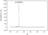
(1)由于本发明所述方法采用双缓冲层技术,即在Si(111)衬底上依次生长AlInN缓冲层、AlN缓冲层,因而进一步减少了AlInN薄膜与衬底的晶格失配,所制备的AlInN薄膜晶体择优取向优异,其XRD图中仅有AlInN(0002)的X射线衍射峰(见图1)。(1) Since the method of the present invention adopts the double buffer layer technology, that is, the AlInN buffer layer and the AlN buffer layer are grown sequentially on the Si(111) substrate, thereby further reducing the lattice mismatch between the AlInN thin film and the substrate, so The prepared AlInN film has excellent crystal preferred orientation, and its XRD pattern has only the X-ray diffraction peak of AlInN (0002) (see Figure 1).
(2)本发明所述方法制备的AlInN薄膜缓冲层厚度较小,AlInN缓冲层和AlN缓冲层的总厚度仅为110nm左右,能够省电节能。(2) The thickness of the buffer layer of the AlInN film prepared by the method of the present invention is small, and the total thickness of the buffer layer of AlInN and the buffer layer of AlN is only about 110nm, which can save electricity and energy.
附图说明Description of drawings
图1是本发明所述方法制备的AlInN薄膜的X射线衍射(XRD)谱图,衬底为Si(111);Fig. 1 is the X-ray diffraction (XRD) spectrogram of the AlInN film that method for the present invention prepares, and substrate is Si(111);
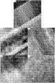
图2是本发明所述方法制备的AlInN薄膜的扫描电镜(SEM)图;Fig. 2 is the scanning electron microscope (SEM) picture of the AlInN thin film prepared by the method of the present invention;
图3是本发明所述方法制备的AlInN薄膜截面的透射电镜(TEM)图〔图中(a)〕和各亚层的高分辨透射电镜(TEM)图〔图中(b)、(c)、(d)、(e)〕。Fig. 3 is the transmission electron microscope (TEM) figure [(a) in the figure] and the high-resolution transmission electron microscope (TEM) figure [(b), (c) of each sublayer of the AlInN thin film section prepared by the method of the present invention , (d), (e)].
具体实施方式Detailed ways
下面通过实施例对本发明所述采用双缓冲层技术制备AlInN薄膜的方法作进一步说明。The method for preparing the AlInN thin film by using the double buffer layer technology of the present invention will be further described through examples below.
实施例Example
本实施例的工艺步骤依次如下:The processing steps of the present embodiment are as follows:
(1)衬底的处理(1) Treatment of the substrate
以Si(111)为衬底,在室温、常压下首先将衬底依次在丙酮中超声波清洗10分钟,在无水乙醇中超声波清洗10分钟,再用去离子水冲洗10分钟,然后在氢氟酸中浸泡5分钟,再用去离子水超声波清洗10分钟,最后用氮气吹干放入溅射室待用。Taking Si(111) as the substrate, at room temperature and normal pressure, the substrate was first ultrasonically cleaned in acetone for 10 minutes, ultrasonically cleaned in absolute ethanol for 10 minutes, then rinsed with deionized water for 10 minutes, and then in hydrogen Soak in hydrofluoric acid for 5 minutes, then ultrasonically clean with deionized water for 10 minutes, and finally blow dry with nitrogen and put it in the sputtering chamber for use.
(2)第一缓冲层AlInN的生长(2) Growth of the first buffer layer AlInN
第一缓冲层AlInN的生长在超高真空多功能磁控溅射设备(型号:JGP560,生产企业:中国科学院沈阳科学仪器研制中心有限公司)中完成,本底真空为4.0×10⁻⁵Pa;将经步骤(1)处理过的Si(111)衬底放入溅射室,在真空条件下采用磁控溅射法在衬底上生长第一缓冲层AlInN,工作气压控制在0.4Pa,靶材为Al0.25In0.75合金,N2为反应气体,Ar为工作气体,N2与Ar分别为14Sccm和2Sccm,溅射功率50W,溅射时间10分钟,溅射过程中衬底的温度控制在300℃;Ar发生电离形成Ar+,Ar+在电磁场作用下碰撞靶材,Ar+与靶材原子交换能量,靶材原子获得的能量大于金属逃逸功时,将离开靶材表面,与反应气体N2反应沉积在衬底表面形成第一缓冲层AlInN;The growth of the first buffer layer AlInN is completed in an ultra-high vacuum multifunctional magnetron sputtering equipment (model: JGP560, manufacturer: Shenyang Scientific Instrument Development Center Co., Ltd., Chinese Academy of Sciences), and the background vacuum is 4.0×10⁻⁵ Pa; Put the Si(111) substrate treated in step (1) into the sputtering chamber, and grow the first buffer layer AlInN on the substrate by magnetron sputtering under vacuum conditions, the working pressure is controlled at 0.4Pa, and the target The material is Al0.25 In0.75 alloy, N2 is the reaction gas, Ar is the working gas, N2 and Ar are 14Sccm and 2Sccm respectively, the sputtering power is 50W, the sputtering time is 10 minutes, and the temperature of the substrate during the sputtering process is controlled at 300°C; Ar is ionized to form Ar+ , Ar+ collides with the target under the action of an electromagnetic field, Ar+ exchanges energy with the target atoms, and when the energy obtained by the target atoms is greater than the work escape work of the metal, they will leave the surface of the target and interact with the reaction gasN2 is reactively deposited on the surface of the substrate to form a first buffer layer AlInN;
(3)第二缓冲层AlN的生长(3) Growth of the second buffer layer AlN
第一缓冲层AlInN生长结束后,将靶材更换为Al(纯度99.8%),工作气压控制在0.4Pa,N2与Ar分别为18.0Sccm和2.0Sccm,溅射功率60W,溅射时间15分钟,溅射过程中衬底的温度控制在500℃;Ar发生电离形成Ar+,Ar+在电磁场作用下碰撞靶材,Ar+与靶材原子交换能量,靶材原子获得的能量大于金属逃逸功时,将离开靶材表面,与反应气体N2反应沉积在第一缓冲层AlInN表面形成第二缓冲层AlN;After the growth of the first buffer layer AlInN is completed, the target is replaced with Al (99.8% purity), the working pressure is controlled at 0.4Pa,N2 and Ar are 18.0Sccm and 2.0Sccm respectively, the sputtering power is 60W, and the sputtering time is 15 minutes , the temperature of the substrate during the sputtering process is controlled at 500°C; Ar is ionized to form Ar+ , Ar+ collides with the target under the action of an electromagnetic field, Ar+ exchanges energy with the target atoms, and the energy obtained by the target atoms is greater than the escape work of the metal , will leave the surface of the target, react with reactive gas N2 and deposit on the surface of the first buffer layer AlInN to form the second buffer layer AlN;
(4)AlInN薄膜的生长(4) Growth of AlInN thin film
第二缓冲层AlN生长结束后,将靶材更换为Al0.5In0.5合金,工作气压控制在0.4Pa,N2与Ar分别为14.0Sccm和2.0Sccm,溅射功率为100W,溅射时间为40分钟,溅射过程中衬底的温度控制在300℃;Ar发生电离形成Ar+,Ar+在电磁场作用下碰撞靶材,Ar+与靶材原子交换能量,靶材原子获得的能量大于金属逃逸功时,将离开靶材表面,与反应气体N2反应沉积在第二缓冲层AlN上形成AlInN薄膜。After the growth of the second buffer layer AlN, the target was replaced with Al0.5 In0.5 alloy, the working pressure was controlled at 0.4Pa, N2 and Ar were 14.0Sccm and 2.0Sccm respectively, the sputtering power was 100W, and the sputtering time was 40 Minutes, the temperature of the substrate during the sputtering process is controlled at 300°C; Ar is ionized to form Ar+ , Ar+ collides with the target under the action of an electromagnetic field, Ar+ exchanges energy with the target atoms, and the energy obtained by the target atoms is greater than the metal escape When working, it will leave the surface of the target, react with the reaction gasN2 and deposit on the second buffer layer AlN to form an AlInN film.
本实例制备的AlInN薄膜的X射线衍射(XRD)谱图见图1(只有AlInN(0002)的一个衍射峰),扫描电镜(SEM)照片见图2,透射电镜(TEM)照片见图3。分析结果表明,采用双缓冲层技术所制备的AlInN薄膜为六方纤锌(wurtzite)结构,晶体生长择优取向优异,(0002)衍射峰位于32.47°,其半峰宽为896arcsec,晶粒大小为36.3nm,[Al]/([Al]+[In])=0.3,方块电阻166.5Ω/□,AlInN缓冲层和AlN缓冲层的总厚度约110nm。The X-ray diffraction (XRD) spectrum of the AlInN film prepared in this example is shown in Figure 1 (only one diffraction peak of AlInN (0002)), the scanning electron microscope (SEM) photo is shown in Figure 2, and the transmission electron microscope (TEM) photo is shown in Figure 3. The analysis results show that the AlInN thin film prepared by the double buffer layer technology has a hexagonal wurtzite structure, and the preferred orientation of crystal growth is excellent. nm, [Al]/([Al]+[In])=0.3, sheet resistance 166.5Ω/□, the total thickness of AlInN buffer layer and AlN buffer layer is about 110nm.
Claims (2)
Priority Applications (1)
| Application Number | Priority Date | Filing Date | Title |
|---|---|---|---|
| CN 201110188036CN102251215B (en) | 2011-07-06 | 2011-07-06 | Method for preparing AlInN film by double buffer layer technique |
Applications Claiming Priority (1)
| Application Number | Priority Date | Filing Date | Title |
|---|---|---|---|
| CN 201110188036CN102251215B (en) | 2011-07-06 | 2011-07-06 | Method for preparing AlInN film by double buffer layer technique |
Publications (2)
| Publication Number | Publication Date |
|---|---|
| CN102251215Atrue CN102251215A (en) | 2011-11-23 |
| CN102251215B CN102251215B (en) | 2013-03-06 |
Family
ID=44978777
Family Applications (1)
| Application Number | Title | Priority Date | Filing Date |
|---|---|---|---|
| CN 201110188036Expired - Fee RelatedCN102251215B (en) | 2011-07-06 | 2011-07-06 | Method for preparing AlInN film by double buffer layer technique |
Country Status (1)
| Country | Link |
|---|---|
| CN (1) | CN102251215B (en) |
Cited By (6)
| Publication number | Priority date | Publication date | Assignee | Title |
|---|---|---|---|---|
| CN103094421A (en)* | 2013-01-28 | 2013-05-08 | 华中科技大学 | Method for improving quality of aluminumnitride (AlN) of face a by utilizing of aluminium nitride indium (AlInN) self-imaging pattern |
| CN103346068A (en)* | 2013-07-11 | 2013-10-09 | 中国科学院半导体研究所 | Method for preparing high In component AlInN thin film |
| WO2015046319A1 (en)* | 2013-09-26 | 2015-04-02 | 三菱マテリアル株式会社 | In ALLOY SPUTTERING TARGET, METHOD FOR PRODUCING SAME, AND In ALLOY FILM |
| TWI614359B (en)* | 2016-06-12 | 2018-02-11 | Method of forming a film and method of forming an aluminum nitride film | |
| CN109786514A (en)* | 2018-12-27 | 2019-05-21 | 华灿光电(浙江)有限公司 | A kind of manufacturing method of LED epitaxial slice |
| CN110344012A (en)* | 2019-07-31 | 2019-10-18 | 沈阳理工大学 | A kind of Al1-xInxN ternary alloy nano crystalline substance film and preparation method thereof |
Citations (3)
| Publication number | Priority date | Publication date | Assignee | Title |
|---|---|---|---|---|
| CN1395291A (en)* | 2002-06-28 | 2003-02-05 | 中国科学院上海微系统与信息技术研究所 | Double buffer layer process for radio-frequency plasma molecular beam epitaxial growth of gallium nitride |
| CN101423927A (en)* | 2008-12-11 | 2009-05-06 | 四川师范大学 | Method for preparing AlxIn1-xN film |
| US20100055883A1 (en)* | 2005-08-30 | 2010-03-04 | Samsung Electro-Mechanics Co., Ltd. | Group iii-nitride semiconductor thin film, method for fabricating the same, and group iii-nitride semiconductor light emitting device |
- 2011
- 2011-07-06CNCN 201110188036patent/CN102251215B/ennot_activeExpired - Fee Related
Patent Citations (3)
| Publication number | Priority date | Publication date | Assignee | Title |
|---|---|---|---|---|
| CN1395291A (en)* | 2002-06-28 | 2003-02-05 | 中国科学院上海微系统与信息技术研究所 | Double buffer layer process for radio-frequency plasma molecular beam epitaxial growth of gallium nitride |
| US20100055883A1 (en)* | 2005-08-30 | 2010-03-04 | Samsung Electro-Mechanics Co., Ltd. | Group iii-nitride semiconductor thin film, method for fabricating the same, and group iii-nitride semiconductor light emitting device |
| CN101423927A (en)* | 2008-12-11 | 2009-05-06 | 四川师范大学 | Method for preparing AlxIn1-xN film |
Cited By (7)
| Publication number | Priority date | Publication date | Assignee | Title |
|---|---|---|---|---|
| CN103094421A (en)* | 2013-01-28 | 2013-05-08 | 华中科技大学 | Method for improving quality of aluminumnitride (AlN) of face a by utilizing of aluminium nitride indium (AlInN) self-imaging pattern |
| CN103346068A (en)* | 2013-07-11 | 2013-10-09 | 中国科学院半导体研究所 | Method for preparing high In component AlInN thin film |
| WO2015046319A1 (en)* | 2013-09-26 | 2015-04-02 | 三菱マテリアル株式会社 | In ALLOY SPUTTERING TARGET, METHOD FOR PRODUCING SAME, AND In ALLOY FILM |
| JP5871106B2 (en)* | 2013-09-26 | 2016-03-01 | 三菱マテリアル株式会社 | In alloy sputtering target, manufacturing method thereof, and In alloy film |
| TWI614359B (en)* | 2016-06-12 | 2018-02-11 | Method of forming a film and method of forming an aluminum nitride film | |
| CN109786514A (en)* | 2018-12-27 | 2019-05-21 | 华灿光电(浙江)有限公司 | A kind of manufacturing method of LED epitaxial slice |
| CN110344012A (en)* | 2019-07-31 | 2019-10-18 | 沈阳理工大学 | A kind of Al1-xInxN ternary alloy nano crystalline substance film and preparation method thereof |
Also Published As
| Publication number | Publication date |
|---|---|
| CN102251215B (en) | 2013-03-06 |
Similar Documents
| Publication | Publication Date | Title |
|---|---|---|
| CN107785241B (en) | A method of preparing beta-gallium oxide film on a silicon substrate | |
| CN105655238B (en) | Silicon based gallium nitride growing method based on graphene Yu magnetron sputtering aluminium nitride | |
| CN102251215A (en) | Method for preparing AlInN film by double buffer layer technique | |
| CN109411328B (en) | Preparation method of gallium oxide film with crystallization temperature reduced by doping iron | |
| CN105161578B (en) | The growing method of GaN film and compound GaN film on Si substrates | |
| CN107706274B (en) | Preparation method of gallium nitride epitaxial structure based on hexagonal boron nitride-graphene composite layer as buffer layer | |
| CN104087909A (en) | Preparation method of cubic silicon carbide film | |
| CN107083540A (en) | A kind of gallium nitride base film on flexible polyimide substrate and preparation method thereof | |
| CN101423927B (en) | A kind of preparation method of AlxIn1-xN film | |
| CN104195514B (en) | Preparation method for zinc tin nitride polycrystalline film | |
| CN108010956A (en) | N polar surfaces high frequency GaN rectifier epitaxial structures and preparation method thereof on a kind of silicon substrate | |
| CN107768235B (en) | A kind of preparation method based on molybdenum disulfide-graphene compound buffer layer epitaxy of gallium nitride structure | |
| CN102268650B (en) | Magnetron sputtering method for preparing indium nitride thin film | |
| CN118028779A (en) | Method for preparing gallium oxide film on silicon substrate | |
| TWI547585B (en) | Method for growing aluminum indium nitride thin film | |
| CN1588631A (en) | Method for preparing high quality ZnO single crystal thin film on (La, Sr) (Al, Ta) O3 | |
| CN103334090B (en) | The preparation method of InN/AlN/ glass structure | |
| CN103352203B (en) | The preparation method of ECR-PEMOCVD low temperature depositing InN film on AlN buffer layer/diamond thin/Si multi-layer film structure substrate | |
| CN103388146B (en) | ECR-PEMOCVD system is to the preparation method of InN/ZnO/ free-standing diamond film structure | |
| CN103388130B (en) | The preparation method of ECR-PEMOCVD low temperature depositing InN film on ZnO buffer/diamond thin/Si multi-layer film structure substrate | |
| CN103352204B (en) | ECR-PEMOCVD system is to the preparation method of InN/GaN/ free-standing diamond film structure | |
| CN103388131B (en) | ECR-PEMOCVD system is to the preparation method of InN/AlN/ free-standing diamond film structure | |
| CN103361629B (en) | The preparation method of ECR-PEMOCVD low temperature depositing InN film on GaN buffer layer/diamond thin/Si multi-layer film structure substrate | |
| CN104037282A (en) | AlGaN film grown on Si substrate, preparation method and application thereof | |
| CN115976644B (en) | Van der Waals epitaxy method of high-quality AlGaN material on amorphous substrate |
Legal Events
| Date | Code | Title | Description |
|---|---|---|---|
| C06 | Publication | ||
| PB01 | Publication | ||
| C10 | Entry into substantive examination | ||
| SE01 | Entry into force of request for substantive examination | ||
| C14 | Grant of patent or utility model | ||
| GR01 | Patent grant | ||
| CF01 | Termination of patent right due to non-payment of annual fee | Granted publication date:20130306 Termination date:20140706 | |
| EXPY | Termination of patent right or utility model |