CN102248756B - Printing system, printing screen plate and printing template contained in printing system, and printing method of printing screen plate and printing template - Google Patents
Printing system, printing screen plate and printing template contained in printing system, and printing method of printing screen plate and printing templateDownload PDFInfo
- Publication number
- CN102248756B CN102248756BCN 201110053493CN201110053493ACN102248756BCN 102248756 BCN102248756 BCN 102248756BCN 201110053493CN201110053493CN 201110053493CN 201110053493 ACN201110053493 ACN 201110053493ACN 102248756 BCN102248756 BCN 102248756B
- Authority
- CN
- China
- Prior art keywords
- shielding layer
- opening
- printing
- substrate
- plate body
- Prior art date
- Legal status (The legal status is an assumption and is not a legal conclusion. Google has not performed a legal analysis and makes no representation as to the accuracy of the status listed.)
- Expired - Fee Related
Links
- 238000007639printingMethods0.000titleclaimsabstractdescription106
- 238000000034methodMethods0.000titleclaimsabstractdescription32
- 239000000758substrateSubstances0.000claimsabstractdescription80
- 239000000463materialSubstances0.000claimsdescription22
- 239000011148porous materialSubstances0.000claimsdescription11
- 239000007769metal materialSubstances0.000claimsdescription5
- 238000009826distributionMethods0.000claimsdescription4
- 206010070834SensitisationDiseases0.000claims1
- 230000008313sensitizationEffects0.000claims1
- 238000006748scratchingMethods0.000abstractdescription3
- 230000002393scratching effectEffects0.000abstractdescription3
- 230000000873masking effectEffects0.000description15
- 238000007650screen-printingMethods0.000description6
- 239000000839emulsionSubstances0.000description5
- 238000010586diagramMethods0.000description4
- 239000004973liquid crystal related substanceSubstances0.000description4
- 230000000694effectsEffects0.000description3
- 239000003292glueSubstances0.000description3
- 238000007790scrapingMethods0.000description3
- 239000000565sealantSubstances0.000description3
- 229910001220stainless steelInorganic materials0.000description3
- 239000010935stainless steelSubstances0.000description3
- 239000011248coating agentSubstances0.000description2
- 238000000576coating methodMethods0.000description2
- 238000005516engineering processMethods0.000description2
- 230000009286beneficial effectEffects0.000description1
- 239000000835fiberSubstances0.000description1
- 239000011521glassSubstances0.000description1
- 238000004519manufacturing processMethods0.000description1
- 239000002184metalSubstances0.000description1
- 238000003825pressingMethods0.000description1
- 238000004080punchingMethods0.000description1
- 239000004065semiconductorSubstances0.000description1
Images


Landscapes
- Printing Plates And Materials Therefor (AREA)
- Printing Methods (AREA)
Abstract
Translated fromChineseDescription
Translated fromChinese技术领域technical field
本发明关于一种印刷系统及其印刷方法;具体而言,本发明关于一种供精密印刷使用的印刷系统及其印刷方法。The present invention relates to a printing system and a printing method thereof; in particular, the present invention relates to a printing system for precision printing and a printing method thereof.
背景技术Background technique
网板印刷的印刷技术已为广泛应用于电子产品中的各类零件,如液晶面板。随着人们对液晶面板等电子产品的需求日益增强,网板印刷技术的成熟度也成为相关产品具备竞争力与否的关键因素。相较于黄光工艺,网板印刷具有加工简单,机台便宜,产距时间(takt time)短等优点。The printing technology of screen printing has been widely used in various parts of electronic products, such as liquid crystal panels. With the increasing demand for electronic products such as liquid crystal panels, the maturity of screen printing technology has become a key factor for the competitiveness of related products. Compared with the yellow light process, screen printing has the advantages of simple processing, cheap machines, and short production time (takt time).
图1A及图1B所示为传统的框胶网板印刷系统。传统的框胶网板印刷机包含有一印刷网板110,供于在一基板100上印刷。基板100包含有设置于基板100上的膜层101。印刷网板110包含有网板本体111及遮蔽层120。网板本体111具有一内面112朝向基板100,而遮蔽层120设置于内面112上。一般遮蔽层120的形成是利用重复涂布多个感光乳剂层于网板本体111的内面112,并一次曝光该多个感光乳剂层形成一遮蔽层印刷图形。FIG. 1A and FIG. 1B show a traditional sealant screen printing system. A conventional screen printing machine includes a
如图1B所示,传统的框胶网板印刷机是利用刮刀140在网板本体111背向基板100的网板面113上,以一刮印的压力将印刷材料150刮印在基板100上。印刷材料150的材质为框胶材质。如图1B所示,印刷材料150通过网板本体111上未被遮蔽层120遮蔽之网眼,以形成框胶160于基板100上。遮蔽层120具有一遮蔽层面121,朝向于基板100。当刮刀140对网板本体111施加刮印压力时,遮蔽层120的遮蔽层面121将接触于基板100上膜层101,刮刀140因此会在刮印过程中刮伤膜层101。如上所述,遮蔽层120是利用一次曝光感光乳剂层而形成,刮印过程中势必会造成膜层101刮伤,影响后续加工良品率。As shown in FIG. 1B , the traditional frame glue screen printing machine uses a scraper 140 to scrape and print the printing material 150 on the
发明内容Contents of the invention
本发明的一个目的在于提供一种印刷系统,达到避免印刷工艺中造成基板上的膜层刮伤的功效。An object of the present invention is to provide a printing system to achieve the effect of avoiding scratches on the film layer on the substrate during the printing process.
本发明的另一个目的在于提供一种印刷网板,供于一基板上进行印刷,可降低损伤基板上膜层的机会。Another object of the present invention is to provide a printing screen for printing on a substrate, which can reduce the chance of damaging the film layer on the substrate.
本发明的另一个目的在于提供一种印刷模板,供于一基板上进行印刷,可降低损伤基板上膜层的机会。Another object of the present invention is to provide a printing template for printing on a substrate, which can reduce the chance of damaging the film layer on the substrate.
本发明的另一个目的在于提供一种印刷方法,供于印刷系统使用,并可达到避免印刷工艺中造成基板上的膜层刮伤的功效。Another object of the present invention is to provide a printing method for use in a printing system, which can achieve the effect of avoiding scratches on the film layer on the substrate during the printing process.
印刷系统包含基板及印刷网板;其中基板上具有形成膜层。印刷网板具有网板本体、第一遮蔽层及第二遮蔽层。网板本体上具有形成多个网眼;第一遮蔽层设置于网板本体面向基板一内面,并部份遮蔽些网板本体的网眼,并形成第一图形开口。第二遮蔽层设置于第一遮蔽层背向基板的一面,并且于第一遮蔽层的覆盖范围形成一容置开口,以朝背向网板本体方向曝露第一遮蔽层。第二遮蔽层上形成一第二图形开口,第二图形开口连通于第一图形开口。第一图形开口及第二图形开口供于印刷时,印刷材料可从网板本体的未被第一遮蔽层所覆盖的网眼,透过第一图形开口及第二图形开口印刷至基板上。当第二遮蔽层接触基板时,容置开口可容纳基板上的膜层,可避免第二遮蔽层刮伤膜层。The printing system includes a substrate and a printing screen; wherein a film layer is formed on the substrate. The printing screen has a screen body, a first shielding layer and a second shielding layer. A plurality of meshes are formed on the screen body; the first shielding layer is arranged on the inner surface of the screen body facing the substrate, and partially covers some meshes of the screen body, and forms a first pattern opening. The second shielding layer is disposed on the side of the first shielding layer facing away from the substrate, and an accommodating opening is formed in the coverage area of the first shielding layer to expose the first shielding layer toward the direction away from the screen main body. A second pattern opening is formed on the second shielding layer, and the second pattern opening communicates with the first pattern opening. When the first pattern opening and the second pattern opening are used for printing, the printing material can be printed onto the substrate through the first pattern opening and the second pattern opening from the mesh of the screen body not covered by the first shielding layer. When the second shielding layer contacts the substrate, the accommodating opening can accommodate the film layer on the substrate, which can prevent the second shielding layer from scratching the film layer.
印刷系统的印刷模板具有一模板本体及一遮蔽层,其中模板本体上形成有多个墨孔。该些墨孔分布形成一第一图形,且该模板本体具有一内面朝向该基板;遮蔽层自该模板本体的该内面突起。其中该遮蔽层并于该第一图形的分布范围外形成一容置开口以曝露该模板本体的该内面。其中,该遮蔽层并形成一第二图形开口连通该些墨孔。The printing template of the printing system has a template body and a shielding layer, wherein a plurality of ink holes are formed on the template body. The ink holes are distributed to form a first pattern, and the template body has an inner surface facing the substrate; the shielding layer protrudes from the inner surface of the template body. Wherein the shielding layer forms an accommodating opening outside the distribution range of the first pattern to expose the inner surface of the template body. Wherein, the shielding layer forms a second pattern opening to communicate with the ink holes.
印刷方法包含于一网板本体上形成一第一遮蔽层以部份遮蔽该网板本体上的多个网眼,并形成第一图形开口;于该第一遮蔽层背向该网板本体的一面上形成一第二遮蔽层及第二图形开口,并于该第一遮蔽层的覆盖范围形成一容置开口以朝背向该网板本体方向曝露该第一遮蔽层;按压该网板本体于该基板上,且该第二遮蔽层接触该基板,使该膜层容纳于该容置开口中;按压该网板本体于该基板时使一印刷物透过第一图形开口与第二图形开口印刷于该基板上。The printing method includes forming a first masking layer on a screen body to partially cover a plurality of meshes on the screen body, and forming a first pattern opening; on the side of the first masking layer facing away from the screen body A second masking layer and a second pattern opening are formed on the top, and an accommodating opening is formed in the coverage area of the first masking layer to expose the first masking layer toward the direction away from the screen body; press the screen body on On the substrate, and the second shielding layer is in contact with the substrate, so that the film layer is accommodated in the accommodating opening; when the screen body is pressed on the substrate, a printed matter is printed through the first pattern opening and the second pattern opening on the substrate.
本发明的有益效果在于:可利用两次曝光方式形成网板本体上的遮蔽层(第一遮蔽层及第二遮蔽层),以制作一容纳区域可容纳基板上的膜层,并避免在印刷过程中刮伤该膜层。The beneficial effect of the present invention is that the shielding layer (the first shielding layer and the second shielding layer) on the screen body can be formed by means of two exposures, so as to make an accommodating area that can accommodate the film layer on the substrate, and avoid printing Scratch the film layer during the process.
以下结合附图和具体实施例对本发明进行详细描述,但不作为对本发明的限定。The present invention will be described in detail below in conjunction with the accompanying drawings and specific embodiments, but not as a limitation of the present invention.
附图说明Description of drawings
图1A及图1B为传统液晶显示装置的印刷系统的示意图;1A and 1B are schematic diagrams of a printing system for a conventional liquid crystal display device;
图2为印刷系统的实施例示意图;Fig. 2 is the schematic diagram of the embodiment of printing system;
图3为印刷系统的另一实施例的示意图;3 is a schematic diagram of another embodiment of a printing system;
图4A、图4B为印刷系统的另一实施例的示意图;及4A and 4B are schematic diagrams of another embodiment of the printing system; and
图5为印刷方法的实施例流程图。FIG. 5 is a flowchart of an embodiment of a printing method.
其中,附图标记Among them, reference signs
100基板100 substrates
101膜层101 film layer
102膜层面102 film level
110印刷网板110 printing screen
111、411网板本体111, 411 stencil body
112内面112 inside
120、420遮蔽层120, 420 shielding layer
121遮蔽层面121 masking level
140刮刀140 scraper
150印刷材料150 printing materials
160框胶160 frame glue
170第一图形开口170 first figure opening
180、184第二图形开口180, 184 second graphic opening
182墨孔182 ink hole
183图形183 graphics
190容置开口190 accommodating openings
220、320第一遮蔽层220, 320 first shielding layer
230、330第二遮蔽层230, 330 second shielding layer
410印刷模板410 printing templates
412内面412 inside
420模板本体420 template body
421第一遮蔽层421 first shielding layer
具体实施方式Detailed ways
下面结合附图和具体实施例对本发明技术方案进行详细的描述,以更进一步了解本发明的目的、方案及功效,但并非作为本发明所附权利要求保护范围的限制。The technical solution of the present invention will be described in detail below in conjunction with the accompanying drawings and specific embodiments to further understand the purpose, solution and effect of the present invention, but it is not intended to limit the scope of protection of the appended claims of the present invention.
本发明提供一种印刷系统及其印刷方法。此外,本发明亦包含使用于上述印刷系统的印刷网板及印刷模板。在较佳实施例中,上述印刷网板及印刷模板可使用于包含液晶面板框胶印刷机等的精密印刷设备及工艺中。The invention provides a printing system and a printing method thereof. In addition, the present invention also includes a printing screen and a printing template used in the above printing system. In a preferred embodiment, the above-mentioned printing screen and printing template can be used in precision printing equipment and processes including liquid crystal panel frame printing machines and the like.
图2所示为本发明的一实施例。如图2所示的一实施例,印刷系统包含基板100及印刷网板110。基板100上具有形成的膜层101。膜层101较佳为半导体加工中形成的各式材质膜层,并利用各式加工形成为不同的电子、电路单元或结构单元。基板100可以为各式透明或不透明基板,材质可为塑料、玻璃或其它材料。印刷网板110具有网板本体111、第一遮蔽层220及第二遮蔽层230。在此实施例中,网板本体111上具有多个网眼。第一遮蔽层220设置于朝向基板100的网板本体111的内面112,并部份遮蔽些网板本体111的网眼。该第二遮蔽层230设置于该第一遮蔽层220朝向该基板100的一面,并且于该第一遮蔽层220的覆盖范围形成一容置开口190以朝背向该网板本体111方向曝露该第一遮蔽层220。第一遮蔽层220的形成是利用曝光重复涂布多个感光乳剂层而形成。第二遮蔽层230的形成是利用第一遮蔽层220形成后,曝光多个感光乳剂层于第一遮蔽层220面向基板100的一面而形成。然而,第一遮蔽层220及第二遮蔽层230亦可以别种材质形成。此外,第一遮蔽层220及第二遮蔽层230两者可采用相同或不相同材料。在较佳实施例中,第一遮蔽层220的厚度小于第二遮蔽层的厚度;然而在其它实施例中,第一遮蔽层220的厚度亦可大于或相当于第二遮蔽层230的厚度。Figure 2 shows an embodiment of the present invention. In one embodiment shown in FIG. 2 , the printing system includes a
在图2所示的实施例中,亦可使该第二遮蔽层230围成该第二图形开口180的侧缘伸入该第一遮蔽层220的该第一图形开口170,并遮蔽该第一遮蔽层220围成该第一图形开口170的侧缘,使该第二遮蔽层230形成的第二图形开口180连通于第一图形开口170。换言之,该第二图形开口180形成于该第一图形开口170内。在较佳实施例中,该第二图形开口180的平均孔径小于该第一图形开口170的平均孔径,并且该第二遮蔽层230的厚度大于该第一遮蔽层220的厚度。为在网板加工对位时减少该印刷网板110与该基板100对位的移位(shift),该第二遮蔽层230的该第二图形开口180较佳为基板100的宽口部181所具有的平均孔径大于该第二图型开口180整体的平均孔径。如图2所示,宽口部181具有一第一厚度而第二图形开口180具有一第二厚度。该第一厚度小于第二厚度。借助此一设计,在印刷过程中不易产生溢墨状况,并使该框胶160的宽度较易控制。In the embodiment shown in FIG. 2, the side edge of the second pattern opening 180 surrounded by the
如图3的实施例所示,印刷网板110具有网板本体111、第一遮蔽层320及第二遮蔽层330。网板本体111上具有形成多个网眼,网眼较佳可由交错的纤维形成;亦可由金属板打孔形成。第一遮蔽层320设置于网板本体111面向该基板100的一内面112,并部份遮蔽些网板本体111的网眼。该第二遮蔽层330设置于该第一遮蔽层320朝向该基板100以上的一面,并且于该第一遮蔽层320的覆盖范围形成一容置开口190以朝背向该网板本体111方向曝露该第一遮蔽层320。As shown in the embodiment of FIG. 3 , the
第一遮蔽层320上具有形成第一图形开口170。第二遮蔽层330上形成一第二图形开口180,第二图形开口180连通于第一图形开口170。利用第一图形开口170及该第二图形开口180的设置,在印刷过程中,印刷材料可自网板本体111未被第一遮蔽层所覆盖的网眼,透过该第一图形开口170及该第二图形开口180印刷至该基板100上。在较佳实施例中,该第二遮蔽层330由较该第一遮蔽层320硬度高的材质制成。在此实施例,该第一遮蔽层320由感光材质形成,而该第二遮蔽层330由金属材质制成,如不锈钢板等材质。然而,如图3所示,该第二遮蔽层330亦可由其它材质制成,并具有一外层331。该外层331较佳以金属材质形成(如不锈钢板等材质)。该第二遮蔽层330的厚度大于该膜层101的高度,使当该第二遮蔽层330接触该基板100时,该外层331不会接触到该基板100上的该膜层101,且容置开口190可容纳该基板上的该膜层101,并可避免第二遮蔽层330刮伤膜层101。A first pattern opening 170 is formed on the
图4A及图4B所示为本发明的另一实施例。图4B所示为图4A的俯视示意图。在此实施例中,印刷模板410具有模板本体420及一遮蔽层421。该模板本体420具有多个墨孔182;该些墨孔182分布形成一第一图形183。模板本体420另具有一内面412朝向该基板100,其中该遮蔽层421自该模板本体420的内面412朝向基板100凸起,并于该第一图形183的分布范围外形成一容置开口190以曝露该模板本体420的该内面412。遮蔽层421并形成一第二图形开口184连通该些墨孔182,其中第二图形开口184为第一图形183相对应。与图2A、2B及图3的前述实施例相比,在此实施例中,模板本体420及遮蔽层421取代了网板本体111、第一遮蔽层320及第二遮蔽层330,然而模板本体420的结构外型仍可与前述实施例相似。在此实施例中,模板本体420可以蚀刻方式制作出遮蔽层421及容置开口190,以保护膜层101。模板本体420及遮蔽层421较佳为金属材质制成,如不锈钢板等材质。在较佳实施例中,容置开口190的深度大于基板100上的膜层101的高度,使当印刷模板410接触基板100时,设置于基板100上的膜层101可完全容纳于容置开口190,并避免膜层101受到刮伤痕迹。4A and 4B show another embodiment of the present invention. FIG. 4B is a schematic top view of FIG. 4A . In this embodiment, the
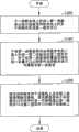
图5所示为印刷方法的实施例流程图。在较佳实施例中,本发明的印刷方法是供于一基板上进行印刷,其中基板上设置有膜层。然而,在其它实施例中,此印刷方法亦可供于其它装置上印刷。FIG. 5 is a flowchart of an embodiment of the printing method. In a preferred embodiment, the printing method of the present invention is used for printing on a substrate, wherein the substrate is provided with a film layer. However, in other embodiments, this printing method can also be used for printing on other devices.
如图5所示,步骤1000包含于网板本体上形成第一遮蔽层,以部分遮蔽网板本体上的多个网眼。第一遮蔽层设置于朝向基板的网板本体内面,并且部分覆盖网板本体内面上的多个网眼。藉此可防止在印刷过程中,印刷材料被印刷在基板上欲印刷部分以外之处。如前述,为控制基板上的印刷范围及图形,第一遮蔽层上形成有第一图形开口。As shown in FIG. 5 ,
步骤1100包含于该第一遮蔽层背向该网板本体的一面上形成第二遮蔽层,并于该第一遮蔽层的覆盖范围形成容置开口以朝背向该网板本体方向曝露该第一遮蔽层。在较佳实施例中,第二遮蔽层可伸入第一图形开口,并遮蔽第一遮蔽层,以围成第一图形开口的侧缘。此外,第二遮蔽层的厚度较佳可形成大于第一遮蔽层的厚度。在较佳实施例中,第二图形开口的平均孔径小于第一图形开口的平均孔径。第二遮蔽层围成第二图形开口的侧缘伸入第一图形开口,并遮蔽第一遮蔽层围成第一图形开口的侧缘。该第二遮蔽层形成第二图形开口,并连通于第一图型开口。第二遮蔽层的厚度可大于基板上的膜层高度。
如图5所示,步骤1200包含按压网板本体于基板上,并当第二遮蔽层接触基板时,使基板上的膜层容纳于容置开口中,并同时使印刷材料透过第一图案开口与第二图案开口印刷于基板上。As shown in FIG. 5,
当然,本发明还可有其它多种实施例,在不背离本发明精神及其实质的情况下,熟悉本领域的技术人员当可根据本发明作出各种相应的改变和变形,但这些相应的改变和变形都应属于本发明所附的权利要求的保护范围。Certainly, the present invention also can have other multiple embodiments, without departing from the spirit and essence of the present invention, those skilled in the art can make various corresponding changes and deformations according to the present invention, but these corresponding Changes and deformations should belong to the scope of protection of the appended claims of the present invention.
Claims (21)
Applications Claiming Priority (2)
| Application Number | Priority Date | Filing Date | Title |
|---|---|---|---|
| TW099147337 | 2010-12-31 | ||
| TW99147337ATWI409173B (en) | 2010-12-31 | 2010-12-31 | A printing system and the printing method thereof |
Publications (2)
| Publication Number | Publication Date |
|---|---|
| CN102248756A CN102248756A (en) | 2011-11-23 |
| CN102248756Btrue CN102248756B (en) | 2013-04-17 |
Family
ID=44976479
Family Applications (1)
| Application Number | Title | Priority Date | Filing Date |
|---|---|---|---|
| CN 201110053493Expired - Fee RelatedCN102248756B (en) | 2010-12-31 | 2011-03-01 | Printing system, printing screen plate and printing template contained in printing system, and printing method of printing screen plate and printing template |
Country Status (2)
| Country | Link |
|---|---|
| CN (1) | CN102248756B (en) |
| TW (1) | TWI409173B (en) |
Families Citing this family (5)
| Publication number | Priority date | Publication date | Assignee | Title |
|---|---|---|---|---|
| CN103203980B (en)* | 2012-01-16 | 2016-10-05 | 昆山允升吉光电科技有限公司 | A kind of metal otter board with multiple step and preparation method thereof |
| TWI454386B (en)* | 2012-09-07 | 2014-10-01 | Motech Ind Inc | Screen plate and method for manufacturing the same |
| CN109492505A (en)* | 2017-09-12 | 2019-03-19 | 南昌欧菲生物识别技术有限公司 | The preparation method of the conductive layer of Printing screen and ultrasonic wave biological identification device |
| CN110103568B (en)* | 2019-06-19 | 2021-03-16 | 赫日光电(苏州)有限公司 | Manufacturing method of laser imaging screen printing plate with stepped opening |
| CN112951953A (en)* | 2019-12-11 | 2021-06-11 | 深圳市聚飞光电股份有限公司 | LED printing method |
Family Cites Families (7)
| Publication number | Priority date | Publication date | Assignee | Title |
|---|---|---|---|---|
| JP2001244616A (en)* | 2000-02-29 | 2001-09-07 | Optrex Corp | Metal mask for printing cream solder |
| JP3825971B2 (en)* | 2000-12-25 | 2006-09-27 | 株式会社ボンマーク | Metal mask for printing |
| TWI458648B (en)* | 2006-04-07 | 2014-11-01 | Mitsubishi Paper Mills Ltd | A method for manufacturing a photographic mask for printing a resin, and a screen printing mask for resin |
| TWI306061B (en)* | 2006-04-27 | 2009-02-11 | Transonic Prec Ind Inc | Multi-layer metal printing stencil and its fabricating method |
| TW200906250A (en)* | 2007-07-27 | 2009-02-01 | Samsung Electro Mech | Mask for screen printing and screen printing method using the same |
| JP5286532B2 (en)* | 2008-10-24 | 2013-09-11 | 株式会社プロセス・ラボ・ミクロン | Paste printing plate |
| JP2010143227A (en)* | 2010-02-05 | 2010-07-01 | Bonmaaku:Kk | Screen printing plate |
- 2010
- 2010-12-31TWTW99147337Apatent/TWI409173B/ennot_activeIP Right Cessation
- 2011
- 2011-03-01CNCN 201110053493patent/CN102248756B/ennot_activeExpired - Fee Related
Also Published As
| Publication number | Publication date |
|---|---|
| CN102248756A (en) | 2011-11-23 |
| TWI409173B (en) | 2013-09-21 |
| TW201226210A (en) | 2012-07-01 |
Similar Documents
| Publication | Publication Date | Title |
|---|---|---|
| CN103250121B (en) | Sensor integrated with glass cover | |
| CN102248756B (en) | Printing system, printing screen plate and printing template contained in printing system, and printing method of printing screen plate and printing template | |
| CN102087472B (en) | Method for fabricating cliche and method for forming thin film pattern by using the same | |
| CN104777665B (en) | The preparation method of black matrix" | |
| US7887997B2 (en) | Manufacturing method for conducting films on two surfaces of transparent substrate of touch control circuit | |
| CN102079162B (en) | Aligning mark and aligning method for screen printing | |
| CN105093636B (en) | Touch display substrate and preparation method thereof and touch-control display panel | |
| CN104238199A (en) | Color film substrate, manufacturing method thereof and display device | |
| CN105974620A (en) | Method for manufacturing substrate, substrate and display device | |
| CN105093806A (en) | Ultraviolet (UV) mask and exposure method thereof | |
| CN106774648A (en) | A kind of mobile terminal 3D glass cover-plates and its ink spraying coating process method | |
| JP5256572B2 (en) | Printing method | |
| CN104614948B (en) | A kind of ultraviolet curing mask plate and preparation method thereof and display device | |
| TW201501594A (en) | Method of manufacturing a high-resolution flexographic printing plate | |
| US9802401B2 (en) | Frame assembly, stencil, screen printing device and screen printing method | |
| KR19980071550A (en) | Printing method and apparatus therefor, and touch panel | |
| WO2025107909A1 (en) | Anti-glare glass and preparation method therefor, and display device | |
| JP5934384B2 (en) | Reverse offset printing plate and manufacturing method thereof | |
| CN201936119U (en) | Novel solder-proof green oil film for printed circuit board | |
| JP6832915B2 (en) | Printing equipment and printing method | |
| CN107238965A (en) | A kind of display panel and preparation method thereof | |
| CN105954939A (en) | Manufacturing method for alignment layer and transfer plate | |
| JP2013086315A (en) | Screen plate for screen printer | |
| CN110854098A (en) | A method for realizing a narrow frame of a display substrate, a narrow frame display substrate, and a metal interconnection method | |
| CN215365506U (en) | Circular hole etching glass |
Legal Events
| Date | Code | Title | Description |
|---|---|---|---|
| C06 | Publication | ||
| PB01 | Publication | ||
| C10 | Entry into substantive examination | ||
| SE01 | Entry into force of request for substantive examination | ||
| C14 | Grant of patent or utility model | ||
| GR01 | Patent grant | ||
| CF01 | Termination of patent right due to non-payment of annual fee | Granted publication date:20130417 Termination date:20210301 | |
| CF01 | Termination of patent right due to non-payment of annual fee |