CN102244107B - Groove capacitor easy to fill and preparation method thereof - Google Patents
Groove capacitor easy to fill and preparation method thereofDownload PDFInfo
- Publication number
- CN102244107B CN102244107BCN201110176559.6ACN201110176559ACN102244107BCN 102244107 BCN102244107 BCN 102244107BCN 201110176559 ACN201110176559 ACN 201110176559ACN 102244107 BCN102244107 BCN 102244107B
- Authority
- CN
- China
- Prior art keywords
- capacitor
- trench
- filling
- easy
- fill
- Prior art date
- Legal status (The legal status is an assumption and is not a legal conclusion. Google has not performed a legal analysis and makes no representation as to the accuracy of the status listed.)
- Active
Links
- 239000003990capacitorSubstances0.000titleclaimsabstractdescription87
- 238000002360preparation methodMethods0.000titleclaimsdescription7
- 239000000463materialSubstances0.000claimsabstractdescription44
- 238000000034methodMethods0.000claimsabstractdescription42
- 239000000758substrateSubstances0.000claimsabstractdescription22
- 230000008021depositionEffects0.000claimsabstractdescription5
- 239000004065semiconductorSubstances0.000claimsdescription17
- 238000000151depositionMethods0.000claimsdescription14
- 239000002184metalSubstances0.000claimsdescription9
- 239000004020conductorSubstances0.000claimsdescription8
- 239000012811non-conductive materialSubstances0.000claimsdescription7
- 239000003292glueSubstances0.000claimsdescription6
- 239000000203mixtureSubstances0.000claimsdescription6
- 238000004528spin coatingMethods0.000claimsdescription6
- 229910000679solderInorganic materials0.000claimsdescription4
- 238000005507sprayingMethods0.000claimsdescription4
- 238000004544sputter depositionMethods0.000claimsdescription4
- 238000005137deposition processMethods0.000claimsdescription3
- 239000003989dielectric materialSubstances0.000claimsdescription3
- 239000011810insulating materialSubstances0.000claimsdescription3
- 239000002923metal particleSubstances0.000claimsdescription3
- 238000003980solgel methodMethods0.000claimsdescription3
- 238000001039wet etchingMethods0.000claimsdescription3
- 239000000919ceramicSubstances0.000claimsdescription2
- 150000001875compoundsChemical class0.000claimsdescription2
- 238000001312dry etchingMethods0.000claimsdescription2
- 239000011521glassSubstances0.000claimsdescription2
- 235000015110jelliesNutrition0.000claimsdescription2
- 239000008274jellySubstances0.000claimsdescription2
- 229920000620organic polymerPolymers0.000claimsdescription2
- 239000002245particleSubstances0.000claimsdescription2
- 239000010409thin filmSubstances0.000claimsdescription2
- 230000000694effectsEffects0.000abstractdescription2
- 238000010586diagramMethods0.000description7
- 230000008569processEffects0.000description5
- 230000006872improvementEffects0.000description4
- 238000004518low pressure chemical vapour depositionMethods0.000description3
- 229910021420polycrystalline siliconInorganic materials0.000description3
- 229920005591polysiliconPolymers0.000description3
- 229910000577Silicon-germaniumInorganic materials0.000description2
- LEVVHYCKPQWKOP-UHFFFAOYSA-N[Si].[Ge]Chemical compound[Si].[Ge]LEVVHYCKPQWKOP-UHFFFAOYSA-N0.000description2
- 230000008901benefitEffects0.000description2
- 230000008859changeEffects0.000description2
- 238000000576coating methodMethods0.000description2
- 238000005429filling processMethods0.000description2
- 150000004767nitridesChemical class0.000description2
- 229910052581Si3N4Inorganic materials0.000description1
- VYPSYNLAJGMNEJ-UHFFFAOYSA-NSilicium dioxideChemical compoundO=[Si]=OVYPSYNLAJGMNEJ-UHFFFAOYSA-N0.000description1
- 230000009286beneficial effectEffects0.000description1
- 230000015572biosynthetic processEffects0.000description1
- 230000015556catabolic processEffects0.000description1
- 239000011248coating agentSubstances0.000description1
- 238000005516engineering processMethods0.000description1
- 238000005530etchingMethods0.000description1
- 230000009969flowable effectEffects0.000description1
- 239000000499gelSubstances0.000description1
- 230000010354integrationEffects0.000description1
- 239000007788liquidSubstances0.000description1
- 239000011344liquid materialSubstances0.000description1
- 238000004519manufacturing processMethods0.000description1
- 238000004377microelectronicMethods0.000description1
- 230000004048modificationEffects0.000description1
- 238000012986modificationMethods0.000description1
- 238000004806packaging method and processMethods0.000description1
- HQVNEWCFYHHQES-UHFFFAOYSA-Nsilicon nitrideChemical compoundN12[Si]34N5[Si]62N3[Si]51N64HQVNEWCFYHHQES-UHFFFAOYSA-N0.000description1
- 229910052814silicon oxideInorganic materials0.000description1
- 239000002904solventSubstances0.000description1
- 238000009271trench methodMethods0.000description1
Images


Landscapes
- Semiconductor Integrated Circuits (AREA)
Abstract
Translated fromChineseDescription
Translated fromChinese技术领域technical field
本发明涉及一种易于填充的沟槽电容以及其制备方法,属于微电子无源器件以及其封装技术领域。The invention relates to an easy-to-fill trench capacitor and a preparation method thereof, belonging to the technical field of microelectronic passive devices and their packaging.
背景技术Background technique
退耦电容器广泛地用于各种电子系统中,它一般连接于电子系统中的供电网络中的电源与地之间,利用电容频率越高阻抗越小的原理,将电源网络中的高频噪声减少,从而对电源网络中的噪声起到抑制作用。实际应用中,由于高密度集成的需要,我们对电容的尺寸大小有限制,一般是希望越小越好,但是小的电容其电容值也相应减小,正是由于其电容值小这一局限性,沟槽式电容的出现就是为了增加有效电容面积从而增大电容密度,如上海宏利半导体制造有限公司金平中等人在“沟槽式金属-绝缘层-金属电容结构与其形成方法”(专利号:CN 1700408)中使用了沟槽方法增加有效的面积利用率与比电容值,台湾茂德科技股份有限公司李岳川等人在“形成沟槽电容于衬底的方法及沟槽电容”(专利号:CN 1862764A)以及华邦电子股份有限公司施本成在“包含沟槽式电容的半导体装置及其制造方法”(专利号:1447437)中也对沟道电容的制程也有详细的描述。沟槽电容的引入同时也会带来电容的填充问题,通过对沟槽电容的填充可以对电容的性能带来以下好处:(1)减小容值在高低温变化下的容值变化(对于大多高K介质的MIM电容);(2)增加结构稳定性;(3)提高击穿性能;Decoupling capacitors are widely used in various electronic systems. They are generally connected between the power supply and the ground in the power supply network in the electronic system. Using the principle that the higher the capacitance frequency, the smaller the impedance, the high-frequency noise in the power supply network Reduced, thereby suppressing the noise in the power network. In practical applications, due to the need for high-density integration, we have restrictions on the size of capacitors. Generally, we hope that the smaller the better, but the capacitance value of a small capacitor is also reduced accordingly, precisely because of the limitation of its small capacitance value. The emergence of trench capacitors is to increase the effective capacitor area and thereby increase the capacitor density. : CN 1700408) used the trench method to increase the effective area utilization rate and specific capacitance value, Li Yuechuan et al. in "Forming Trench Capacitance on Substrate and Trench Capacitance" (Patent No. : CN 1862764A) and Shi Bencheng of Winbond Electronics Co., Ltd. also described the process of trench capacitance in detail in "Semiconductor Device Including Trench Capacitor and Its Manufacturing Method" (Patent No.: 1447437). The introduction of the trench capacitor will also bring about the problem of filling the capacitor. The filling of the trench capacitor can bring the following benefits to the performance of the capacitor: (1) Reduce the capacitance change under high and low temperature changes (for Most high-K dielectric MIM capacitors); (2) increase structural stability; (3) improve breakdown performance;
常见的对沟槽结构电容的填充方法按照填充材料特性不同以及方法不同有多种,如专利US6204089B1、US6,359,300 B1采用CVD或者LPCVD方法完成填充,填充的结构为一个上方带焊盘的电容结构,填充材料为重掺杂导电的Ge或者GeSi混合物。US6,194,755 B1也提到采用沉积方法填充多晶硅;Nxp和Philip公司提到采用LPCVD方法完成填充,填充的材料为绝缘材料氧化硅或者氮化硅 ,以及导电材料为代表的导电金属或导电重掺杂半导体。当沟槽结构在大孔径下也可以采用真空填充设备来完成真空填充技术。而这些传统的填充方法均存在以下的共同问题:(1)填充存在的空洞,(2)传统方法需要经过300-500℃高温,或者真空等条件,(3)填充材料为多晶硅,氧化物,氮化物,硅锗混合物等,工艺昂贵且难以控制。Common filling methods for trench structure capacitors vary according to the characteristics of the filling material and different methods. For example, patents US6204089B1 and US6,359,300 B1 use CVD or LPCVD to complete the filling. The filled structure is a capacitor structure with a pad on the top. , the filling material is heavily doped conductive Ge or GeSi mixture. US6,194,755 B1 also mentions that polysilicon is filled by deposition; Nxp and Philip companies mention that LPCVD is used to complete the filling, and the filling material is insulating material silicon oxide or silicon nitride, and conductive metal or conductive heavy doping represented by conductive material Miscellaneous semiconductors. When the trench structure is under large aperture, vacuum filling equipment can also be used to complete the vacuum filling technology. These traditional filling methods all have the following common problems: (1) filling the existing voids, (2) traditional methods need to go through high temperature of 300-500 ℃, or vacuum conditions, etc., (3) the filling materials are polysilicon, oxide, Nitride, silicon germanium mixture, etc., the process is expensive and difficult to control.
发明内容Contents of the invention
本发明针对传统的填充方法均存在以上的共同问题的不足,提供一种易于在常温常压下实现填充的沟槽电容的结构以及其制备方法。The present invention aims at the disadvantages of the above-mentioned common problems in the traditional filling methods, and provides a trench capacitor structure and a preparation method that can be easily filled at normal temperature and pressure.
为达到上述目的,本发明提供一种易于填充的沟槽电容包括:电容衬底,位于所述电容衬底上的多个相互连通的沟槽,位于所述电容衬底的表面上的下电极,位于所述下电极的表面上的介质层,位于所述介质层的表面上的上电极,以及填充于沟槽处的填充材料,所述填充材料位于上电极的表面上。To achieve the above object, the present invention provides an easy-to-fill trench capacitor comprising: a capacitor substrate, a plurality of interconnected grooves positioned on the capacitor substrate, and a lower electrode positioned on the surface of the capacitor substrate , a dielectric layer located on the surface of the lower electrode, an upper electrode located on the surface of the dielectric layer, and a filling material filled in the groove, the filling material located on the surface of the upper electrode.
在上述技术方案的基础上,本发明还可以做如下改进。On the basis of the above technical solutions, the present invention can also be improved as follows.
进一步,所述电容为的金属-薄膜-金属电容、半导体结电容或者存在以沟槽构成功能的电容器;所述电容衬底为陶瓷、半导体材料、化合物材料或者玻璃材料;所述电容为分立电容、或者为电容衬底上嵌入的电容。Further, the capacitor is a metal-film-metal capacitor, a semiconductor junction capacitor, or a capacitor with a trench function; the capacitor substrate is ceramic, semiconductor material, compound material or glass material; the capacitor is a discrete capacitor , or a capacitor embedded on a capacitor substrate.
进一步,还包括一个或者多个互联结构,该互联结构使所有的沟槽相互连通形成一个整体连接,所述互联结构和沟槽的宽度为1微米~100微米,所述互联结构和沟槽的深度为1微米~100微米。Further, it also includes one or more interconnection structures, the interconnection structure makes all the trenches communicate with each other to form an integral connection, the width of the interconnection structure and the trench is 1 micron to 100 micron, the interconnection structure and the trench The depth is from 1 micron to 100 microns.
进一步,所述填充材料为导电材料或者非导电材料;所述导电材料为导电胶、导电钎料或者导电金属颗粒混合物;所述非导电材料为有机聚合物、胶状物或者绝缘材料;所述填充材料的最小颗粒直径小于或者等于互联结构的最小尺寸宽度;所述填充材料状态为具有可流动性的状态,且经100℃~200℃高温固化或者100℃~200℃回流后形成稳固的填充。Further, the filling material is a conductive material or a non-conductive material; the conductive material is a conductive glue, a conductive solder or a mixture of conductive metal particles; the non-conductive material is an organic polymer, jelly or insulating material; the The minimum particle diameter of the filling material is less than or equal to the minimum dimension width of the interconnection structure; the state of the filling material is in a flowable state, and a stable filling is formed after being cured at a high temperature of 100°C to 200°C or reflowed at 100°C to 200°C .
本发明还提供一种易于填充的沟槽电容的制备方法包括如下步骤:The present invention also provides a method for preparing an easy-to-fill trench capacitance comprising the steps of:
步骤1:在电容衬底表面上形成多个相互连通的沟槽;Step 1: forming a plurality of interconnected grooves on the surface of the capacitor substrate;
步骤2:在沟槽的表面上形成下电极;Step 2: forming a lower electrode on the surface of the trench;
步骤3:在下电极的表面上沉积介质层;Step 3: depositing a dielectric layer on the surface of the lower electrode;
步骤4:在介质层的表面上形成上电极;Step 4: forming an upper electrode on the surface of the dielectric layer;
步骤5:在沟槽处填充材料,所述填充材料位于上电极的表面上;Step 5: Filling the groove with material, the filling material is located on the surface of the upper electrode;
步骤6:填充后经100℃~200℃高温固化或者100℃~200℃回流后,形成稳定的沟槽电容。Step 6: After filling, solidify at a high temperature of 100°C to 200°C or reflow at 100°C to 200°C to form a stable trench capacitor.
进一步,所述步骤1通过干法刻蚀、湿法刻蚀、机械或者激光的方法形成可连通结构的沟槽。Further, in the step 1, grooves that can communicate with the structure are formed by dry etching, wet etching, mechanical or laser methods.
进一步,所述步骤2中通过沉积一层导电金属、重掺杂形成一层低电阻率的半导体、或者选择沉积重掺杂半导体材料以形成下电极。Further, in the step 2, the lower electrode is formed by depositing a layer of conductive metal, heavily doping to form a layer of low-resistivity semiconductor, or selectively depositing heavily doped semiconductor material.
进一步,所述步骤3通过使用沉积工艺、溅射、旋涂或者溶胶凝胶工艺将电容介电材料或者铁电薄膜材料形成在下电极上;如果为结电容,其介电层直接通过掺杂形成空间电容区,进而形成耗尽层。Further, in step 3, a capacitor dielectric material or a ferroelectric thin film material is formed on the lower electrode by using a deposition process, sputtering, spin coating or sol-gel process; if it is a junction capacitor, its dielectric layer is directly formed by doping The space capacitance region, and then forms the depletion layer.
进一步,所述步骤4中通过沉积一层导电金属、重掺杂形成一层低电阻率的半导体、或者选择沉积重掺杂半导体材料以形成下电极。Further, in step 4, the lower electrode is formed by depositing a layer of conductive metal, heavily doping to form a layer of low-resistivity semiconductor, or selectively depositing heavily doped semiconductor material.
进一步,所述步骤5中填充材料的方法为在20℃~25℃时,一个标准大气压下的点胶方法、旋涂法或者喷涂法。Further, the method of filling the material in the step 5 is a dispensing method, a spin coating method or a spray coating method under a standard atmospheric pressure at 20°C to 25°C.
本发明的有益效果是:本发明电容结构的主要特征为:将电容的沟槽形成特殊的图形,在不损失电容有效表面积,即电容值的前提下,通过沟槽结构的改变,形成易于填充的沟槽结构,最终在该结构上形成电容,引出电极,最后在常温常压下即在20℃~25℃时,一个标准大气压下通过简单的方法填充电容的沟槽间隙,填充效果不存在气泡或者空洞等问题,形成稳固的电容结构。本发明与常见的沟槽结构电容的结构以及其填充方法相比有以下项优点:首先,本发明不同于传统的传统方法均需要依靠LPCVD或者其他沉积溅射设备,需要经过300~500℃高温,所需设备及其工艺昂贵且难以控制,本发明直接在常温常压下采用点胶或者涂敷工艺即可完成填充过程;传统的填充材料为多晶硅,氧化物,氮化物,硅锗混合物等作为导电材料,本发明直接利用导电胶或者钎料溶剂直接流入连通结构中,最后通过高温固化或者回流形成填充,操作简单易行;传统的填充容易产生空洞气泡等问题,本发明利用形成的独特的连通结构,在不改变原来沟槽结构表面积的情况下,可以将填充变的简单且填充质量良好。The beneficial effect of the present invention is that: the main feature of the capacitor structure of the present invention is: the groove of the capacitor is formed into a special pattern, and under the premise of not losing the effective surface area of the capacitor, that is, the capacitance value, through the change of the groove structure, an easy-to-fill The groove structure of the capacitor is finally formed on the structure, and the electrodes are drawn out. Finally, at normal temperature and pressure, that is, at 20°C to 25°C, the gap of the capacitor’s groove is filled by a simple method under a standard atmospheric pressure, and the filling effect does not exist. Bubbles or cavities and other problems are eliminated to form a stable capacitive structure. Compared with the structure of the common trench structure capacitor and its filling method, the present invention has the following advantages: First, the present invention is different from the traditional traditional method, which needs to rely on LPCVD or other deposition and sputtering equipment, and needs to go through a high temperature of 300-500°C , the required equipment and its process are expensive and difficult to control. The present invention can directly complete the filling process by dispensing or coating process at normal temperature and pressure; traditional filling materials are polysilicon, oxide, nitride, silicon-germanium mixture, etc. As a conductive material, the present invention directly uses conductive glue or solder solvent to flow directly into the connected structure, and finally solidifies at high temperature or reflows to form filling, which is simple and easy to operate; traditional filling is prone to problems such as voids and bubbles, and the present invention utilizes the unique formed The connected structure can make the filling simple and the filling quality good without changing the surface area of the original trench structure.
附图说明Description of drawings
图1为本发明实施例中采用点胶方法实现填充电容沟槽连通结构的方法示意图;Fig. 1 is the schematic diagram of the method for realizing the connection structure of the capacitor groove by using the dispensing method in the embodiment of the present invention;
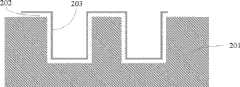
图2a至图2e为本发明实施例易于填充的沟槽电容及其填充方法的工艺过程对应的结构示意图;2a to 2e are structural schematic diagrams corresponding to the process of the easy-to-fill trench capacitor and its filling method according to the embodiment of the present invention;
图3a至图3f为本发明实施例易于填充的沟槽电容以及相对于未作改进之前图形的实例和说明的结构示意图。FIGS. 3a to 3f are structural schematic diagrams of examples and descriptions of trench capacitors that are easy to fill in accordance with an embodiment of the present invention, as well as examples and illustrations relative to the pattern without improvement.
具体实施方式Detailed ways
以下结合附图对本发明的原理和特征进行描述,所举实例只用于解释本发明,并非用于限定本发明的范围。The principles and features of the present invention are described below in conjunction with the accompanying drawings, and the examples given are only used to explain the present invention, and are not intended to limit the scope of the present invention.
图1为本发明实施例中采用点胶方法实现填充电容沟槽连通结构的方法示意图。如图1所示,电容衬底101上刻蚀出多个相互连通的沟槽,再通过简单方法完成对这些连通沟槽的预填充,预填充时采用的填充材料102一般为液态或者凝胶状可流动性材料,本实施方法以点胶方法为例,借用点胶工具103,将填充材料滴入沟槽区域,使填充材料在结构中形成一个可连通的整体,然后待填满后,可通过100℃~200℃高温固化或者100℃~200℃回流形成稳固的填充。FIG. 1 is a schematic diagram of a method for filling a connected structure of a capacitance trench by using a dispensing method in an embodiment of the present invention. As shown in FIG. 1, a plurality of interconnected grooves are etched on the
图2a至图2e为本发明实施例易于填充的沟槽电容及其填充方法的工艺过程对应的结构示意图;2a to 2e are structural schematic diagrams corresponding to the process of the easy-to-fill trench capacitor and its filling method according to the embodiment of the present invention;
步骤1,如图2a所示,在电容衬底表面201上形成多个沟槽,接着在已经形成沟槽结构的电容衬底表面201上形成互联结构,该互联结构是多个沟槽之间相互连通,该沟槽结构和互联结构的形成可以为各种干法,湿法刻蚀,也可以为机械或者激光的方法来完成,该沟槽结构和互联结构的最小宽度为1个微米,最大可为1百个微米,该沟槽结构和互联结构深度也在1个微米至1百个微米之间;Step 1, as shown in FIG. 2a, a plurality of grooves are formed on the
步骤2,如图2b所示,在图形表面形成下电极202,其电容下电极形成方法可以为沉积一层导电金属,也可为重掺杂形成一层低电阻率的半导体,也可以选择重掺杂半导体为基板,沉积绝缘层以形成下电极部分;Step 2, as shown in Figure 2b, forms the
步骤3,如图2c所示,在下电极的表面沉积电容介质层203,其形成方法一般为沉积工艺或者溅射,旋涂以及溶胶凝胶工艺等。如果为结电容,其绝缘介电部分直接通过掺杂可形成空间电容区,进而形成耗尽层,不需要单独沉积介电材料;Step 3, as shown in FIG. 2 c , deposits a capacitive
步骤4,如图2d所示,在电容介质层表面形成上电极204,其形成方法为在电容介质的有效区域沉积一层导电金属,也可为重掺杂形成一层低电阻率的半导体,也可以选择沉积一层重掺杂半导体材料以形成下电极部分。Step 4, as shown in FIG. 2d, an
步骤5,如图2e所示,在电容的沟槽处填充材料205,其填充方法可为在20℃~25℃时,一个标准大气压下的点胶方法,如图1所示,或者其他旋涂以及喷涂的方法,直接将具有一定流动性的材料流入结构中,由于整个沟槽结构形成相互连通的结构,所以在填充的过程中不存在空洞气泡,直接通过液态材料的流动最后赶走空气。Step 5, as shown in Figure 2e, fills the groove of the capacitor with
步骤6,最后根据填充的方法或者材料,在完成填充后,经过100℃~200℃高温固化或者100℃~200℃回流后,形成稳定的电容结构。Step 6. Finally, according to the filling method or material, after the filling is completed, a stable capacitor structure is formed after high-temperature curing at 100°C to 200°C or reflow at 100°C to 200°C.
图3a至图3f为本发明实施例易于填充的沟槽电容以及相对于未作改进之前图形的实例和说明的结构示意图;其中,301为沟槽电容衬底部分;302为沟槽电容的中需要纵向刻蚀掉形成沟槽结构的图形部分。Fig. 3 a to Fig. 3 f are the trench capacitors that are easy to fill in the embodiment of the present invention and the structural diagrams of the examples and descriptions of the graphics before no improvement; wherein, 301 is the substrate part of the trench capacitor; 302 is the center of the trench capacitor The portion of the pattern forming the trench structure needs to be etched away longitudinally.
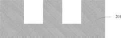
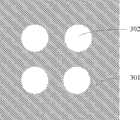
如图3a,3c所示,为未做改进之前的传统圆孔和沟道结构,各个圆孔之间形成各自独立的小结构,如图3b,3d所示,为改进后的可连通型的结构,可以看出电容表面即未作改变,只是变化刻蚀部分,即可获得连通的易于填充的结构。As shown in Figures 3a and 3c, it is the traditional circular hole and channel structure before improvement, and each independent small structure is formed between each circular hole, as shown in Figure 3b and 3d, it is an improved connectable Structure, it can be seen that the surface of the capacitor has not been changed, only the etched part is changed, and a connected and easy-to-fill structure can be obtained.
如图3e,3f所示,为其他图示的电容表面沟槽结构,主要目的也是将各种形状的图形练成一体,在刻蚀的时候同时完成,在填充的时候形成连通体。另外有其他的各种结构或者形状可,只要是以形成连通为目的的结构,均为本专利的保护范围之类,在这里不做更多图示说明。As shown in Figures 3e and 3f, the trench structures on the surface of capacitors shown in other diagrams are mainly used to integrate various shapes of graphics into one body, which are completed at the same time when etching, and form connected bodies when filling. In addition, there are various other structures or shapes, as long as the structure is for the purpose of forming a connection, they are all within the scope of protection of this patent, and no more illustrations are given here.
以上所述仅为本发明的较佳实施例,并不用以限制本发明,凡在本发明的精神和原则之内,所作的任何修改、等同替换、改进等,均应包含在本发明的保护范围之内。The above descriptions are only preferred embodiments of the present invention, and are not intended to limit the present invention. Any modifications, equivalent replacements, improvements, etc. made within the spirit and principles of the present invention shall be included in the protection of the present invention. within range.
Claims (12)
Translated fromChinesePriority Applications (1)
| Application Number | Priority Date | Filing Date | Title |
|---|---|---|---|
| CN201110176559.6ACN102244107B (en) | 2011-06-28 | 2011-06-28 | Groove capacitor easy to fill and preparation method thereof |
Applications Claiming Priority (1)
| Application Number | Priority Date | Filing Date | Title |
|---|---|---|---|
| CN201110176559.6ACN102244107B (en) | 2011-06-28 | 2011-06-28 | Groove capacitor easy to fill and preparation method thereof |
Publications (2)
| Publication Number | Publication Date |
|---|---|
| CN102244107A CN102244107A (en) | 2011-11-16 |
| CN102244107Btrue CN102244107B (en) | 2014-06-18 |
Family
ID=44962059
Family Applications (1)
| Application Number | Title | Priority Date | Filing Date |
|---|---|---|---|
| CN201110176559.6AActiveCN102244107B (en) | 2011-06-28 | 2011-06-28 | Groove capacitor easy to fill and preparation method thereof |
Country Status (1)
| Country | Link |
|---|---|
| CN (1) | CN102244107B (en) |
Families Citing this family (2)
| Publication number | Priority date | Publication date | Assignee | Title |
|---|---|---|---|---|
| CN105006362B (en)* | 2015-07-28 | 2018-06-19 | 桂林电子科技大学 | A kind of thin film capacitor preparation method of peelable substrate |
| EP3627535B1 (en) | 2018-08-08 | 2022-06-22 | Shenzhen Weitongbo Technology Co., Ltd. | Trench capacitor and method for manufacturing same |
Citations (4)
| Publication number | Priority date | Publication date | Assignee | Title |
|---|---|---|---|---|
| CN1303132A (en)* | 1999-12-14 | 2001-07-11 | 株式会社东芝 | MIM capacitor |
| US6387750B1 (en)* | 2001-07-02 | 2002-05-14 | Macronix International Co., Ltd. | Method of forming MIM capacitor |
| CN1738025A (en)* | 2004-08-17 | 2006-02-22 | 因芬尼昂技术股份公司 | Method of manufacturing traces with increased capacitive coupling and corresponding traces |
| CN101604692A (en)* | 2008-06-09 | 2009-12-16 | 阿尔特拉公司 | Method and apparatus for creating deep trench capacitors to improve device performance |
Family Cites Families (3)
| Publication number | Priority date | Publication date | Assignee | Title |
|---|---|---|---|---|
| JPS63140560A (en)* | 1986-12-02 | 1988-06-13 | Mitsubishi Electric Corp | Semiconductor monolithic bias power supply circuit |
| US6720232B1 (en)* | 2003-04-10 | 2004-04-13 | Taiwan Semiconductor Manufacturing Company | Method of fabricating an embedded DRAM for metal-insulator-metal (MIM) capacitor structure |
| US7989958B2 (en)* | 2005-06-14 | 2011-08-02 | Cufer Assett Ltd. L.L.C. | Patterned contact |
- 2011
- 2011-06-28CNCN201110176559.6Apatent/CN102244107B/enactiveActive
Patent Citations (4)
| Publication number | Priority date | Publication date | Assignee | Title |
|---|---|---|---|---|
| CN1303132A (en)* | 1999-12-14 | 2001-07-11 | 株式会社东芝 | MIM capacitor |
| US6387750B1 (en)* | 2001-07-02 | 2002-05-14 | Macronix International Co., Ltd. | Method of forming MIM capacitor |
| CN1738025A (en)* | 2004-08-17 | 2006-02-22 | 因芬尼昂技术股份公司 | Method of manufacturing traces with increased capacitive coupling and corresponding traces |
| CN101604692A (en)* | 2008-06-09 | 2009-12-16 | 阿尔特拉公司 | Method and apparatus for creating deep trench capacitors to improve device performance |
Also Published As
| Publication number | Publication date |
|---|---|
| CN102244107A (en) | 2011-11-16 |
Similar Documents
| Publication | Publication Date | Title |
|---|---|---|
| TWI373913B (en) | Applying trenched transient voltage suppressor (tvs) technology for distributed low pass filters | |
| US11417594B2 (en) | 3DIC package integration for high-frequency RF system | |
| CN103311141B (en) | A kind of manufacture method of coaxial vertical interconnection conductor | |
| CN104108679A (en) | Method Of Manufacturing Through-glass Vias | |
| CN117525044B (en) | Three-dimensional capacitor unit structure, three-dimensional capacitor and three-dimensional chip integrated structure thereof | |
| CN102244107B (en) | Groove capacitor easy to fill and preparation method thereof | |
| CN103787264B (en) | The manufacture method of a kind of silicon via devices being applied to high-speed wideband light network and device thereof | |
| CN106997878A (en) | The silicon capacitor and its manufacture method of double-decker | |
| CN105990095B (en) | MIM capacitor and preparation method thereof | |
| CN103972217A (en) | Integrated passive capacitance fan-out-type wafer-level packaging structure and manufacturing method thereof | |
| CN105895507B (en) | Radio frequency capacity cell based on silicon-on-insulator substrate and preparation method thereof | |
| CN103426728B (en) | Capacitor arrangement and preparation method thereof | |
| CN104659113B (en) | The interior matching capacitance and manufacture method of RFLDMOS devices | |
| CN103904054B (en) | Interconnection structure based on glass substrate and method | |
| US8026111B2 (en) | Dielectric enhancements to chip-to-chip capacitive proximity communication | |
| CN117334480A (en) | Film flat capacitor and preparation method and application thereof | |
| CN103956326A (en) | Manufacturing method for integrated passive interposer and corresponding integrated passive interposer | |
| CN203871322U (en) | Silicon through hole device applied to high speed broadband optical interconnection | |
| CN109326655B (en) | Semiconductor varactor and manufacturing method thereof | |
| CN105097769B (en) | A kind of device of three dimensional integrated circuits and preparation method thereof | |
| CN105448743B (en) | A kind of production method of molybdenum disulfide field-effect tube | |
| TWI542019B (en) | Pressure sensor and manufacture method thereof | |
| CN107170750A (en) | A kind of semiconductor components and devices structure and preparation method thereof | |
| CN106952895B (en) | A kind of manufacturing method of MIM capacitor structure | |
| CN106449355A (en) | Trench capacitor and production method thereof |
Legal Events
| Date | Code | Title | Description |
|---|---|---|---|
| C06 | Publication | ||
| PB01 | Publication | ||
| C10 | Entry into substantive examination | ||
| SE01 | Entry into force of request for substantive examination | ||
| C14 | Grant of patent or utility model | ||
| GR01 | Patent grant | ||
| ASS | Succession or assignment of patent right | Owner name:CHENGDU RHOPTICS OPTOELECTRONIC TECHNOLOGY CO., LT Free format text:FORMER OWNER: INST OF MICROELECTRONICS, C. A. S Effective date:20140806 | |
| C41 | Transfer of patent application or patent right or utility model | ||
| COR | Change of bibliographic data | Free format text:CORRECT: ADDRESS; FROM: 100029 CHAOYANG, BEIJING TO: 610041 CHENGDU, SICHUAN PROVINCE | |
| TR01 | Transfer of patent right | Effective date of registration:20140806 Address after:610041, Sichuan, Chengdu hi tech Development Zone, 188 Rui Rui Road, No. 6, No. 2 building Patentee after:CHENGDU RUIHUA OPTOELECTRONIC TECHNOLOGY Co.,Ltd. Address before:100029 Beijing city Chaoyang District Beitucheng West Road No. 3 Institute of Microelectronics Patentee before:Institute of Microelectronics of the Chinese Academy of Sciences | |
| TR01 | Transfer of patent right | ||
| TR01 | Transfer of patent right | Effective date of registration:20210218 Address after:214028 building D1, China Sensor Network International Innovation Park, No. 200, Linghu Avenue, New District, Wuxi City, Jiangsu Province Patentee after:National Center for Advanced Packaging Co.,Ltd. Address before:2 / F, no.188-6, Zirui Avenue, Chengdu hi tech Development Zone, Sichuan 610041 Patentee before:CHENGDU RUIHUA OPTOELECTRONIC TECHNOLOGY Co.,Ltd. |