CN102237359A - Semiconductor device - Google Patents
Semiconductor deviceDownload PDFInfo
- Publication number
- CN102237359A CN102237359ACN2011101044183ACN201110104418ACN102237359ACN 102237359 ACN102237359 ACN 102237359ACN 2011101044183 ACN2011101044183 ACN 2011101044183ACN 201110104418 ACN201110104418 ACN 201110104418ACN 102237359 ACN102237359 ACN 102237359A
- Authority
- CN
- China
- Prior art keywords
- diffusion layer
- layer
- wiring
- drain
- cmos inverter
- Prior art date
- Legal status (The legal status is an assumption and is not a legal conclusion. Google has not performed a legal analysis and makes no representation as to the accuracy of the status listed.)
- Granted
Links
- 239000004065semiconductorSubstances0.000titleclaimsabstractdescription118
- 238000009792diffusion processMethods0.000claimsabstractdescription279
- 239000000758substrateSubstances0.000claimsabstractdescription38
- 238000002955isolationMethods0.000claimsdescription15
- 239000010410layerSubstances0.000description436
- XUIMIQQOPSSXEZ-UHFFFAOYSA-NSiliconChemical compound[Si]XUIMIQQOPSSXEZ-UHFFFAOYSA-N0.000description105
- 229910052710siliconInorganic materials0.000description105
- 239000010703siliconSubstances0.000description105
- 238000004519manufacturing processMethods0.000description46
- 229910021332silicideInorganic materials0.000description20
- FVBUAEGBCNSCDD-UHFFFAOYSA-Nsilicide(4-)Chemical compound[Si-4]FVBUAEGBCNSCDD-UHFFFAOYSA-N0.000description20
- 238000005520cutting processMethods0.000description9
- 239000011159matrix materialSubstances0.000description7
- 238000005229chemical vapour depositionMethods0.000description5
- 238000005468ion implantationMethods0.000description5
- 229910052785arsenicInorganic materials0.000description4
- RQNWIZPPADIBDY-UHFFFAOYSA-Narsenic atomChemical compound[As]RQNWIZPPADIBDY-UHFFFAOYSA-N0.000description4
- 238000005516engineering processMethods0.000description4
- 229910052751metalInorganic materials0.000description4
- 239000002184metalSubstances0.000description4
- 229910044991metal oxideInorganic materials0.000description4
- 150000004706metal oxidesChemical class0.000description4
- 230000010354integrationEffects0.000description3
- 239000011229interlayerSubstances0.000description3
- 238000000034methodMethods0.000description3
- 238000000926separation methodMethods0.000description3
- 239000000126substanceSubstances0.000description3
- 238000001039wet etchingMethods0.000description3
- 229910015900BF3Inorganic materials0.000description2
- 229910052581Si3N4Inorganic materials0.000description2
- VYPSYNLAJGMNEJ-UHFFFAOYSA-NSilicium dioxideChemical compoundO=[Si]=OVYPSYNLAJGMNEJ-UHFFFAOYSA-N0.000description2
- WTEOIRVLGSZEPR-UHFFFAOYSA-Nboron trifluorideChemical compoundFB(F)FWTEOIRVLGSZEPR-UHFFFAOYSA-N0.000description2
- 230000000295complement effectEffects0.000description2
- 238000001312dry etchingMethods0.000description2
- 238000005530etchingMethods0.000description2
- 238000010438heat treatmentMethods0.000description2
- 239000012535impuritySubstances0.000description2
- 238000009413insulationMethods0.000description2
- 238000005498polishingMethods0.000description2
- HQVNEWCFYHHQES-UHFFFAOYSA-Nsilicon nitrideChemical compoundN12[Si]34N5[Si]62N3[Si]51N64HQVNEWCFYHHQES-UHFFFAOYSA-N0.000description2
- 229910052814silicon oxideInorganic materials0.000description2
- 238000004544sputter depositionMethods0.000description2
- ZOXJGFHDIHLPTG-UHFFFAOYSA-NBoronChemical compound[B]ZOXJGFHDIHLPTG-UHFFFAOYSA-N0.000description1
- QVGXLLKOCUKJST-UHFFFAOYSA-Natomic oxygenChemical compound[O]QVGXLLKOCUKJST-UHFFFAOYSA-N0.000description1
- 230000009286beneficial effectEffects0.000description1
- 229910052796boronInorganic materials0.000description1
- 239000011248coating agentSubstances0.000description1
- 238000000576coating methodMethods0.000description1
- 150000001875compoundsChemical class0.000description1
- 238000010586diagramMethods0.000description1
- 229910052732germaniumInorganic materials0.000description1
- GNPVGFCGXDBREM-UHFFFAOYSA-Ngermanium atomChemical compound[Ge]GNPVGFCGXDBREM-UHFFFAOYSA-N0.000description1
- 239000007943implantSubstances0.000description1
- 230000002452interceptive effectEffects0.000description1
- 238000001459lithographyMethods0.000description1
- 239000000203mixtureSubstances0.000description1
- 238000012986modificationMethods0.000description1
- 230000004048modificationEffects0.000description1
- 150000004767nitridesChemical class0.000description1
- 229910052760oxygenInorganic materials0.000description1
- 239000001301oxygenSubstances0.000description1
- 230000003071parasitic effectEffects0.000description1
- 229910021420polycrystalline siliconInorganic materials0.000description1
- 229920005591polysiliconPolymers0.000description1
- 238000007738vacuum evaporationMethods0.000description1
Images


Classifications
- H—ELECTRICITY
- H10—SEMICONDUCTOR DEVICES; ELECTRIC SOLID-STATE DEVICES NOT OTHERWISE PROVIDED FOR
- H10D—INORGANIC ELECTRIC SEMICONDUCTOR DEVICES
- H10D84/00—Integrated devices formed in or on semiconductor substrates that comprise only semiconducting layers, e.g. on Si wafers or on GaAs-on-Si wafers
- H10D84/80—Integrated devices formed in or on semiconductor substrates that comprise only semiconducting layers, e.g. on Si wafers or on GaAs-on-Si wafers characterised by the integration of at least one component covered by groups H10D12/00 or H10D30/00, e.g. integration of IGFETs
- H10D84/82—Integrated devices formed in or on semiconductor substrates that comprise only semiconducting layers, e.g. on Si wafers or on GaAs-on-Si wafers characterised by the integration of at least one component covered by groups H10D12/00 or H10D30/00, e.g. integration of IGFETs of only field-effect components
- H10D84/83—Integrated devices formed in or on semiconductor substrates that comprise only semiconducting layers, e.g. on Si wafers or on GaAs-on-Si wafers characterised by the integration of at least one component covered by groups H10D12/00 or H10D30/00, e.g. integration of IGFETs of only field-effect components of only insulated-gate FETs [IGFET]
- H10D84/85—Complementary IGFETs, e.g. CMOS
- H10D84/853—Complementary IGFETs, e.g. CMOS comprising FinFETs
- H—ELECTRICITY
- H10—SEMICONDUCTOR DEVICES; ELECTRIC SOLID-STATE DEVICES NOT OTHERWISE PROVIDED FOR
- H10D—INORGANIC ELECTRIC SEMICONDUCTOR DEVICES
- H10D30/00—Field-effect transistors [FET]
- H10D30/60—Insulated-gate field-effect transistors [IGFET]
- H10D30/62—Fin field-effect transistors [FinFET]
- H—ELECTRICITY
- H10—SEMICONDUCTOR DEVICES; ELECTRIC SOLID-STATE DEVICES NOT OTHERWISE PROVIDED FOR
- H10D—INORGANIC ELECTRIC SEMICONDUCTOR DEVICES
- H10D30/00—Field-effect transistors [FET]
- H10D30/60—Insulated-gate field-effect transistors [IGFET]
- H10D30/67—Thin-film transistors [TFT]
- H10D30/6729—Thin-film transistors [TFT] characterised by the electrodes
- H10D30/673—Thin-film transistors [TFT] characterised by the electrodes characterised by the shapes, relative sizes or dispositions of the gate electrodes
- H10D30/6735—Thin-film transistors [TFT] characterised by the electrodes characterised by the shapes, relative sizes or dispositions of the gate electrodes having gates fully surrounding the channels, e.g. gate-all-around
- H—ELECTRICITY
- H10—SEMICONDUCTOR DEVICES; ELECTRIC SOLID-STATE DEVICES NOT OTHERWISE PROVIDED FOR
- H10D—INORGANIC ELECTRIC SEMICONDUCTOR DEVICES
- H10D84/00—Integrated devices formed in or on semiconductor substrates that comprise only semiconducting layers, e.g. on Si wafers or on GaAs-on-Si wafers
- H10D84/01—Manufacture or treatment
- H10D84/0123—Integrating together multiple components covered by H10D12/00 or H10D30/00, e.g. integrating multiple IGBTs
- H10D84/0126—Integrating together multiple components covered by H10D12/00 or H10D30/00, e.g. integrating multiple IGBTs the components including insulated gates, e.g. IGFETs
- H10D84/0165—Integrating together multiple components covered by H10D12/00 or H10D30/00, e.g. integrating multiple IGBTs the components including insulated gates, e.g. IGFETs the components including complementary IGFETs, e.g. CMOS devices
- H10D84/0193—Integrating together multiple components covered by H10D12/00 or H10D30/00, e.g. integrating multiple IGBTs the components including insulated gates, e.g. IGFETs the components including complementary IGFETs, e.g. CMOS devices the components including FinFETs
- H—ELECTRICITY
- H10—SEMICONDUCTOR DEVICES; ELECTRIC SOLID-STATE DEVICES NOT OTHERWISE PROVIDED FOR
- H10D—INORGANIC ELECTRIC SEMICONDUCTOR DEVICES
- H10D84/00—Integrated devices formed in or on semiconductor substrates that comprise only semiconducting layers, e.g. on Si wafers or on GaAs-on-Si wafers
- H10D84/01—Manufacture or treatment
- H10D84/0123—Integrating together multiple components covered by H10D12/00 or H10D30/00, e.g. integrating multiple IGBTs
- H10D84/0126—Integrating together multiple components covered by H10D12/00 or H10D30/00, e.g. integrating multiple IGBTs the components including insulated gates, e.g. IGFETs
- H10D84/0165—Integrating together multiple components covered by H10D12/00 or H10D30/00, e.g. integrating multiple IGBTs the components including insulated gates, e.g. IGFETs the components including complementary IGFETs, e.g. CMOS devices
- H10D84/0195—Integrating together multiple components covered by H10D12/00 or H10D30/00, e.g. integrating multiple IGBTs the components including insulated gates, e.g. IGFETs the components including complementary IGFETs, e.g. CMOS devices the components including vertical IGFETs
- H—ELECTRICITY
- H10—SEMICONDUCTOR DEVICES; ELECTRIC SOLID-STATE DEVICES NOT OTHERWISE PROVIDED FOR
- H10D—INORGANIC ELECTRIC SEMICONDUCTOR DEVICES
- H10D84/00—Integrated devices formed in or on semiconductor substrates that comprise only semiconducting layers, e.g. on Si wafers or on GaAs-on-Si wafers
- H10D84/01—Manufacture or treatment
- H10D84/02—Manufacture or treatment characterised by using material-based technologies
- H10D84/03—Manufacture or treatment characterised by using material-based technologies using Group IV technology, e.g. silicon technology or silicon-carbide [SiC] technology
- H10D84/038—Manufacture or treatment characterised by using material-based technologies using Group IV technology, e.g. silicon technology or silicon-carbide [SiC] technology using silicon technology, e.g. SiGe
- H—ELECTRICITY
- H10—SEMICONDUCTOR DEVICES; ELECTRIC SOLID-STATE DEVICES NOT OTHERWISE PROVIDED FOR
- H10D—INORGANIC ELECTRIC SEMICONDUCTOR DEVICES
- H10D84/00—Integrated devices formed in or on semiconductor substrates that comprise only semiconducting layers, e.g. on Si wafers or on GaAs-on-Si wafers
- H10D84/80—Integrated devices formed in or on semiconductor substrates that comprise only semiconducting layers, e.g. on Si wafers or on GaAs-on-Si wafers characterised by the integration of at least one component covered by groups H10D12/00 or H10D30/00, e.g. integration of IGFETs
- H10D84/82—Integrated devices formed in or on semiconductor substrates that comprise only semiconducting layers, e.g. on Si wafers or on GaAs-on-Si wafers characterised by the integration of at least one component covered by groups H10D12/00 or H10D30/00, e.g. integration of IGFETs of only field-effect components
- H10D84/83—Integrated devices formed in or on semiconductor substrates that comprise only semiconducting layers, e.g. on Si wafers or on GaAs-on-Si wafers characterised by the integration of at least one component covered by groups H10D12/00 or H10D30/00, e.g. integration of IGFETs of only field-effect components of only insulated-gate FETs [IGFET]
- H10D84/85—Complementary IGFETs, e.g. CMOS
- H—ELECTRICITY
- H10—SEMICONDUCTOR DEVICES; ELECTRIC SOLID-STATE DEVICES NOT OTHERWISE PROVIDED FOR
- H10D—INORGANIC ELECTRIC SEMICONDUCTOR DEVICES
- H10D89/00—Aspects of integrated devices not covered by groups H10D84/00 - H10D88/00
- H10D89/10—Integrated device layouts
Landscapes
- Metal-Oxide And Bipolar Metal-Oxide Semiconductor Integrated Circuits (AREA)
Abstract
Translated fromChinese
Description
Translated fromChinese本案依据2010年4月21日申请的美国专利临时申请61/326,339号、及2010年4月21日申请的日本国专利申请2010-97735号主张优先权,参酌该申请案揭示的内容而全部援用。This case claims priority based on U.S. Patent Provisional Application No. 61/326,339 filed on April 21, 2010, and Japanese Patent Application No. 2010-97735 filed on April 21, 2010, all of which are cited with reference to the content disclosed in the application .
技术领域technical field
本发明涉及一种半导体器件,特别是关于一种具有柱状半导体,将其侧壁作为沟道区域,并采用以使栅极电极包围沟道区域的方式形成的纵型MOS(Metal Oxide Semiconductor;金属氧化物半导体)晶体管的环绕栅极晶体管(Surrounding Gate Transistor;SGT)的CMOS(Complementary Metal-OxideSemiconductor;互补式金属氧化物半导体)反向器(inverter)中、特别是以2段以上串联连接的CMOS反向器。The present invention relates to a semiconductor device, in particular to a vertical MOS (Metal Oxide Semiconductor; Metal Oxide Semiconductor) that has a columnar semiconductor, uses its sidewall as a channel region, and adopts a method in which a gate electrode surrounds the channel region. In the CMOS (Complementary Metal-Oxide Semiconductor; Complementary Metal-Oxide Semiconductor) inverter (Surrounding Gate Transistor; SGT) of the Surrounding Gate Transistor (SGT) of the oxide semiconductor) transistor, especially the CMOS connected in series with more than two stages reverser.
背景技术Background technique
为了实现半导体器件的高集成化与高性能化,提出有一种具备形成在半导体衬底的表面的柱状半导体层、及以包围该柱状半导体层的方式形成在该柱状半导体层的侧壁的栅极的纵型栅极晶体管的SGT(参照例如日本特开平2-188966号公报、S.Watanabe等,“A Nobel Circuit Technology withSurrounding Gate Transistors(SGT’s)for Ultra High Density DRAM’s”(一种使用SGT的超高密度DRAM的新型电路技术),IEEE JSSC,第30卷、第9期、1995年9月.)。在SGT中,漏极、栅极、源极配置在垂直方向。因此,SGT相较于现有技术的平面(planar)型晶体管,可大幅地缩小占有面积。In order to achieve higher integration and higher performance of semiconductor devices, a semiconductor device comprising a columnar semiconductor layer formed on the surface of a semiconductor substrate and a gate electrode formed on the sidewall of the columnar semiconductor layer so as to surround the columnar semiconductor layer has been proposed. The SGT of the vertical gate transistor (refer to Japanese Patent Application Publication No. 2-188966, S. Watanabe, etc., "A Nobel Circuit Technology with Surrounding Gate Transistors (SGT's) for Ultra High Density DRAM's" (a kind of ultra high density DRAM's using SGT) Novel Circuit Technology for Density DRAM), IEEE JSSC, Vol. 30, No. 9, September 1995.). In SGT, the drain, gate, and source are arranged vertically. Therefore, compared with the planar transistors in the prior art, the SGT can greatly reduce the occupied area.
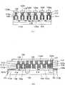
使用SGT的CMOS反向器的一例为揭示在日本特开平2-188966号公报。图37中(A)为显示揭示在日本特开平2-188966号公报的CMOS反向器的平面,图37中(B)为显示图37中(A)的切割线A-A’的剖面。An example of a CMOS inverter using SGT is disclosed in Japanese Patent Application Laid-Open No. 2-188966. Fig. 37(A) is a plan showing the CMOS inverter disclosed in Japanese Patent Application Laid-Open No. 2-188966, and Fig. 37(B) is a cross section showing cutting line A-A' of Fig. 37(A).
在图37中(A)、图37中(B)中,在硅衬底301形成有N阱(well)302及P阱303。在N阱302区域形成有用以形成PMOS(Positive ChannelMetal-Oxide-Semiconductor)QP的柱状硅层305,在P阱303区域形成有用以形成NMOS(Negative Channel Metal-Oxide-Semiconductor)QN的柱状硅层306。以分别包围柱状硅层305及柱状硅层306的方式形成有栅极308及元件分离区域304。形成在用以形成PMOS的柱状硅层305的下部的P+漏极扩散层310、及形成在用以形成NMOS的柱状硅层306的下部的N+漏极扩散层312连接在输出端子Vout。形成在用以形成PMOS的柱状硅层305的上部的P+源极扩散层309通过Vcc配线层314而连接在电源电位Vcc,形成在用以形成NMOS的柱状硅层306的上部的N+源极扩散层311通过Vss配线层315而连接在接地电位VSS,PMOS与NMOS的共通栅极308连接在输入端子(Vin)316。通过上述构成,形成CMOS反向器。In FIG. 37(A) and FIG. 37(B), an N well 302 and a
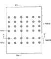
就串联连接2段以上的CMOS反向器的例子而言,图38中(A)为显示2段CMOS反向器的平面,图38中(B)为显示图38中(A)的切割线A-A’的剖面(参照S.Watanabe等.,“A Nobel Circuit Technology with Surrounding GateTransistors(SGT’s)for Ultra High Density DRAM’s”(一种使用SGT的超高密度DRAM的新型电路技术),IEEE JSSC,第30卷、第9期、1995年9月)。As an example of connecting two or more stages of CMOS inverters in series, (A) in Fig. 38 shows the plane of the two-stage CMOS inverter, and (B) in Fig. 38 shows the cutting line in (A) in Fig. 38 A-A' section (refer to S. Watanabe et al., "A Nobel Circuit Technology with Surrounding Gate Transistors (SGT's) for Ultra High Density DRAM's" (a new circuit technology using SGT's ultra-high density DRAM), IEEE JSSC, Vol. 30, No. 9, September 1995).
在图38中(A)、图38中(B)中,在硅衬底形成有P+扩散层418及N+扩散层419。对P+扩散层418从配线层436施加电源电位Vcc,对N+扩散层419从配线层435施加接地电位Vss。在P+扩散层418上形成有构成PMOS的柱状硅层411至414。在N+扩散层419上形成有构成NMOS的柱状硅层415至417。第1段的反向器以由柱状硅层413、414所构成的PMOS、及由柱状硅层415所构成的NMOS来形成。在这些柱状硅层413、414、415的周围形成有共通的栅极422。通过配线层433及形成在栅极422上的接触部(contact)426,对栅极422施加该第1段的反向器的输入电压。此外,从形成在柱状硅层413、414、415上的接触部429、430,对配线层437施加该第1段的反向器的输出电压。In FIG. 38(A) and FIG. 38(B), a
第2段的反向器由通过柱状硅层411、412而构成的PMOS、及通过柱状硅层416、417而构成的NMOS所形成。在柱状硅层411、412的周围形成有栅极421。在柱状硅层416、417的周围形成有栅极423。通过配线层437及形成在栅极上的接触部427,对栅极421施加该第2段的反向器的输入电压,通过配线层437及形成在栅极上的接触部428,对栅极423施加该第2段的反向器的输入电压。此外,通过形成在柱状硅层411、412、416、417上的接触部431、432,对配线层434施加该第2段的反向器的输出电压。The inverter of the second stage is formed of PMOS formed by the
在该第2段反向器中,连接施加有电源电位Vcc的配线层436与P+扩散层418的接触部424、及连接施加有接地电位Vss的配线层435与N+扩散层419的接触部425所占有的面积较大。因此,该2段反向器的占有面积较大。In this second-stage inverter, the
此外,就串联连接成2段以上的CMOS反向器的其他例而言,图39中(A)为显示日本特开2009-38226号公报揭示的CMOS反向器链的平面,图39中(B)为显示图39中(A)的切割线A-A’的剖面。In addition, in terms of other examples of CMOS inverters connected in series in two or more stages, (A) in FIG. B) is a section showing the cutting line AA' of (A) in FIG. 39 .
在图39中(A)、图39中(B)中,在氧化硅膜(SiO2膜)上形成有构成PMOS的柱状半导体层511、512、515、516、517、518、521、522、及构成NMOS的柱状半导体层513、514、519、520。第1段的反向器通过以柱状半导体层521、522所构成的PMOS、及以柱状半导体层520所构成的NMOS而形成。在这些柱状半导体层520、521,522的周围形成有共通的栅极530。电源电位通过配线层535施加至形成在构成PMOS的柱状半导体层521、522的上部的扩散层,接地电位通过配线层534施加至形成在构成NMOS的柱状半导体层520的上部的扩散层。第2段的反向器通过以柱状半导体层517、518所构成的PMOS、及以柱状半导体层519所构成的NMOS而形成。在这些柱状半导体层517、518、519的周围形成有共通的栅极529。对栅极529从下部配线层525施加输入电位。电源电位从配线层533施加至形成在构成PMOS的柱状半导体层517、518的上部的扩散层,接地电位从配线层534施加至形成在构成NMOS的柱状半导体层519的上部的扩散层。In FIG. 39(A) and FIG. 39(B),
通过反复以上的单位构造,从柱状半导体层511至522、下部配线层523至526、栅极527至530、配线层531至535形成反向器链。By repeating the above unit structure, an inverter chain is formed from the
在该现有技术例中,构成电路的扩散层与栅极配线的布局复杂。此外,由于NMOS与PMOS交互配置在狭窄的区域,因此在使用于微细化至数10nm程级的器件时,难以形成集成度高的反向器。再者,日本特开2009-38226号公报提出一种为了增加并排形成的柱的个数而并联连接图39的整体反向器电路。然而,在此情形时,由于连接无助于提升元件分离区域等的直接器件的能力的部分都反复配置,因此无法有效率地增加并联形成的柱的个数。In this prior art example, the layout of the diffusion layer and the gate wiring constituting the circuit is complicated. In addition, since NMOS and PMOS are alternately arranged in a narrow area, it is difficult to form a highly integrated inverter when it is used in a device miniaturized to several 10 nm. Furthermore, Japanese Patent Application Laid-Open No. 2009-38226 proposes a parallel connection of the integral inverter circuit of FIG. 39 in order to increase the number of columns formed side by side. However, in this case, it is not possible to efficiently increase the number of columns formed in parallel because parts that do not contribute to improving the performance of direct devices such as element isolation regions are repeatedly arranged.
如以上说明,现有技术提出的串联连接成2段以上的CMOS反向器的构造有对占有面积的缩小进行更进一步的改进的必要。As explained above, the structure of CMOS inverters connected in series in two or more stages proposed in the prior art requires further improvement in reducing the occupied area.
发明内容Contents of the invention
(发明所欲解决的问题)(Problem to be solved by the invention)
鉴于现有技术中存在的问题,本发明的目的在于实现占有面积小的串联连接有2段以上的CMOS反向器。In view of the problems existing in the prior art, the object of the present invention is to realize a CMOS inverter having more than two stages connected in series with a small occupied area.
(解决问题的手段)(means to solve the problem)
为了达成所述目的,本发明的第1实施方式的半导体器件为一种具备结合有至少2段以上的CMOS反向器的CMOS反向器结合电路的半导体器件,所述CMOS反向器由纵型MOS晶体管所构成,该纵型MOS晶体管的源极扩散层、漏极扩散层及柱状半导体层相对于衬底阶层性地配置在垂直方向,所述柱状半导体层配置在所述源极扩散层与所述漏极扩散层之间,且在所述柱状半导体层的侧壁形成有栅极电极;所述CMOS反向器结合电路包含:第1段的第1CMOS反向器,由排列在衬底上的第1列(column)的多个纵型MOS晶体管所构成;及第2段的第2CMOS反向器,由排列在所述衬底上的第2列的多个纵型MOS晶体管所构成;排列在所述第1列的多个纵型MOS晶体管[A1]由形成在第1N+源极扩散层上的1个或多个第1NMOS纵型晶体管、及形成在第1P+源极扩散层上的1个或多个第1PMOS纵型晶体管所构成,所述第1N+源极扩散层与所述第1P+源极扩散层彼此邻接而形成,在所述第1N+源极扩散层输入有第1电位,在所述第1P+源极扩散层输入有第2电位,所述1个或多个第1NMOS纵型晶体管的栅极电极与所述1个或多个第1PMOS纵型晶体管的栅极电极相连接,且形成第1栅极配线,在所述第1栅极配线的端部,形成有用以将输入电压输入至所述第1CMOS反向器的第1接触部,且在构成所述1个或多个第1NMOS纵型晶体管的柱状半导体层的上部,形成有第1N+漏极扩散层,在所述第1N+漏极扩散层上,形成有连接所述第1N+漏极扩散层与用以输出所述第1反向器的输出电压的第1配线层的第2接触部,在构成所述1个或多个第1PMOS纵型晶体管的柱状半导体层的上部,形成有第1P+漏极扩散层,在所述第1P+漏极扩散层上,形成有连接所述第1P+漏极扩散层与用以输出所述第1反向器的输出电压的第1配线层的第3接触部,排列在所述第2列的多个纵型MOS晶体管由形成在所述第1N+源极扩散层上的1个或多个第2的NMOS纵型晶体管、及形成在所述第1P+源极扩散层上的1个或多个第2PMOS纵型晶体管所形成,所述1个或多个第2NMOS纵型晶体管的栅极电极、与所述1个或多个第2PMOS纵型晶体管的栅极电极相连接,且形成第2栅极配线,在所述第2栅极配线上的另一方端部,形成有用以将输入电压输入至所述第2CMOS反向器的第4接触部,所述第4接触部与所述第1配线层相连接,在构成所述1个或多个第2NMOS纵型晶体管的柱状半导体层的上部,形成有第2N+漏极扩散层,在所述第2N+漏极扩散层上,形成有连接所述第2N+漏极扩散层与用以输出所述第2CMOS反向器的输出电压的第2配线层的第5接触部,在构成所述1个或多个第2PMOS纵型晶体管的柱状半导体层的上部,形成有第2P+漏极扩散层,在所述第2P+漏极扩散层上,形成有连接所述第2P+漏极扩散层与用以输出所述第2CMOS反向器的输出电压的第2配线层的第6接触部,所述第1CMOS反向器与所述第2CMOS反向器交互结合。In order to achieve the above object, the semiconductor device according to the first embodiment of the present invention is a semiconductor device including a CMOS inverter combination circuit in which at least two or more stages of CMOS inverters are combined, and the CMOS inverters are composed of vertical type MOS transistor, the source diffusion layer, the drain diffusion layer and the columnar semiconductor layer of the vertical MOS transistor are arranged in a vertical direction relative to the substrate, and the columnar semiconductor layer is arranged on the source diffusion layer. A gate electrode is formed between the drain diffusion layer and on the sidewall of the columnar semiconductor layer; the CMOS inverter combination circuit includes: the first CMOS inverter of the first segment, which is arranged on the substrate a plurality of vertical MOS transistors in the first column (column) on the bottom; and a second CMOS inverter in the second segment is formed by a plurality of vertical MOS transistors in the second column arranged on the substrate Composition; the plurality of vertical MOS transistors [A1] arranged in the first column are formed on one or more first NMOS vertical transistors formed on the first N+ source diffusion layer, and one or more first NMOS vertical transistors formed on the first P+ source diffusion layer One or more first PMOS vertical transistors above, the first N+ source diffusion layer and the first P+ source diffusion layer are formed adjacent to each other, and the first N+ source diffusion layer is input with the first Potential, a second potential is input to the first P+ source diffusion layer, the gate electrodes of the one or more first NMOS vertical transistors are connected to the gate electrodes of the one or more first PMOS vertical transistors are connected to each other, and form a first gate wiring. At the end of the first gate wiring, a first contact for inputting an input voltage to the first CMOS inverter is formed. A first N+ drain diffusion layer is formed on the upper part of the columnar semiconductor layer of the one or more first NMOS vertical transistors, and a layer connecting the first N+ drain diffusion layer and the first N+ drain diffusion layer is formed on the first N+ drain diffusion layer. The second contact portion of the first wiring layer for outputting the output voltage of the first inverter is formed with a first P+ A drain diffusion layer, on the first P+ drain diffusion layer, a third wiring layer connecting the first P+ drain diffusion layer and the first wiring layer for outputting the output voltage of the first inverter is formed. In the contact part, the plurality of vertical MOS transistors arranged in the second column are composed of one or more second NMOS vertical transistors formed on the first N+ source diffusion layer, and one or more second NMOS vertical transistors formed on the first P+ One or more second PMOS vertical transistors on the source diffusion layer, the gate electrodes of the one or more second NMOS vertical transistors, and the one or more second PMOS vertical transistors The gate electrodes are connected to form a second gate wiring, and a fourth contact for inputting an input voltage to the second CMOS inverter is formed at the other end of the second gate wiring. portion, the fourth contact portion is connected to the first wiring layer, and constitutes the one or more second N On the upper part of the columnar semiconductor layer of the MOS vertical transistor, a 2nd N+ drain diffusion layer is formed, and on the 2nd N+ drain diffusion layer, a layer connecting the 2nd N+ drain diffusion layer and the second CMOS layer for outputting the 2nd CMOS is formed. The fifth contact portion of the second wiring layer of the output voltage of the inverter is formed with a second P+ drain diffusion layer on the upper part of the columnar semiconductor layer constituting the one or more second PMOS vertical transistors. A sixth contact portion connecting the second P+ drain diffusion layer and the second wiring layer for outputting the output voltage of the second CMOS inverter is formed on the second P+ drain diffusion layer, and the first CMOS The inverter is interactively combined with the second CMOS inverter.
为了达成所述目的,本发明的第2实施方式的半导体器件为一种具备结合有至少2段以上的CMOS反向器的CMOS反向器结合电路的半导体器件,所述CMOS反向器由纵型MOS晶体管所构成,该纵型MOS晶体管的源极扩散层、漏极扩散层及柱状半导体层相对于衬底阶层性地配置在垂直方向,所述柱状半导体层配置在所述源极扩散层与所述漏极扩散层之间,且在所述柱状半导体层的侧壁形成有栅极电极;所述CMOS反向器结合电路包含:第1段的第1CMOS反向器,由排列在衬底上的第1列的多个纵型MOS晶体管所构成;及第2段的第2CMOS反向器,由排列在所述衬底上的第2列的多个纵型MOS晶体管所构成;排列在所述第1列的多个纵型MOS晶体管[A2]由形成在第1N+源极扩散层上的1个或多个第1NMOS纵型晶体管、及形成在第1P+源极扩散层上的1个或多个第1PMOS纵型晶体管所构成,所述第1N+源极扩散层与所述第1P+源极扩散层彼此邻接而形成,在所述第1N+源极扩散层输入有第1电位,在所述第1P+源极扩散层输入有第2电位,所述1个或多个第1NMOS纵型晶体管的栅极电极与所述1个或多个第2PMOS纵型晶体管的栅极电极相连接,且形成第1栅极配线,在所述第1栅极配线上,于形成在所述第1N+源极扩散层与所述第1P+源极扩散层之间的元件分离上的区域中,形成有用以将输入电压输入至所述第1CMOS反向器的第1接触部,且在形成所述1个或多个第1NMOS纵型晶体管的柱状半导体层的上部,形成有第1N+漏极扩散层,在所述第1N+漏极扩散层上,形成有连接所述第1N+漏极扩散层与用以输出所述第1反向器的输出电压的第1配线层的第2接触部,在构成所述1个或多个第1PMOS纵型晶体管的柱状半导体层的上部,形成有第1P+漏极扩散层,在所述第1P+漏极扩散层上,形成有连接所述第1P+漏极扩散层与用以输出所述第1反向器的输出电压的第2配线层的第3接触部,排列在所述第2列的多个纵型MOS晶体管由形成在所述第1N+源极扩散层上的1个或多个第2NMOS纵型晶体管、及形成在所述第1P+源极扩散层上的1个或多个第2PMOS纵型晶体管所形成,所述1个或多个第2NMOS纵型晶体管的栅极电极、与所述1个或多个第2PMOS纵型晶体管的栅极电极相连接,且形成第2栅极配线,在所述第2栅极配线上的一方端部,形成有用以将输入电压输入至所述第2CMOS反向器的第4接触部,所述第4接触部与所述第1配线层相连接,在所述第2栅极配线上的另一方端部形成有用以将输入电压输入至所述第2CMOS反向器的第5接触部,且所述第5接触部与所述第2配线层相连接,在形成所述1个或多个第2NMOS纵型晶体管的柱状半导体层的上部,形成有第2N+漏极扩散层,在所述第2N+漏极扩散层上,形成有连接所述第2N+漏极扩散层与用以输出所述第2CMOS反向器的输出电压的第3配线层的第6接触部,在构成所述1个或多个第2PMOS纵型晶体管的柱状半导体层的上部,形成有第2P+漏极扩散层,在所述第2P+漏极扩散层上,形成有连接所述第2P+漏极扩散层与用以输出所述第2CMOS反向器的输出电压的第3配线层的第7接触部,所述第1CMOS反向器与所述第2CMOS反向器交互结合。In order to achieve the above object, the semiconductor device according to the second embodiment of the present invention is a semiconductor device including a CMOS inverter combination circuit in which at least two or more stages of CMOS inverters are combined, and the CMOS inverters are composed of vertical type MOS transistor, the source diffusion layer, the drain diffusion layer and the columnar semiconductor layer of the vertical MOS transistor are arranged in a vertical direction relative to the substrate, and the columnar semiconductor layer is arranged on the source diffusion layer. A gate electrode is formed between the drain diffusion layer and on the sidewall of the columnar semiconductor layer; the CMOS inverter combination circuit includes: the first CMOS inverter of the first segment, which is arranged on the substrate a plurality of vertical MOS transistors in the first column on the bottom; and a second CMOS inverter in the second segment, which is composed of a plurality of vertical MOS transistors in the second column arranged on the substrate; the arrangement The plurality of vertical MOS transistors [A2] in the first column are composed of one or more first NMOS vertical transistors formed on the first N+ source diffusion layer and one formed on the first P+ source diffusion layer. One or more first PMOS vertical transistors, the first N+ source diffusion layer and the first P+ source diffusion layer are formed adjacent to each other, a first potential is input to the first N+ source diffusion layer, and The first P+ source diffusion layer is input with a second potential, the gate electrodes of the one or more first NMOS vertical transistors are connected to the gate electrodes of the one or more second PMOS vertical transistors, And forming a first gate wiring, on the first gate wiring, in a region formed on the element isolation between the first N+ source diffusion layer and the first P+ source diffusion layer, A first contact portion for inputting an input voltage to the first CMOS inverter is formed, and a first N+ drain diffusion is formed on the upper part of the columnar semiconductor layer forming the one or more first NMOS vertical transistors. layer, on the first N+ drain diffusion layer, a second contact portion connecting the first N+ drain diffusion layer and the first wiring layer for outputting the output voltage of the first inverter is formed, A first P+ drain diffusion layer is formed on the upper part of the columnar semiconductor layer constituting the one or more first PMOS vertical transistors, and a first P+ drain diffusion layer is formed on the first P+ drain diffusion layer to connect the first P+ drain. The third contact portion between the diffusion layer and the second wiring layer for outputting the output voltage of the first inverter, the plurality of vertical MOS transistors arranged in the second column are formed on the first N+ source One or more second NMOS vertical transistors on the pole diffusion layer and one or more second PMOS vertical transistors formed on the first P+ source diffusion layer, the one or more first The gate electrodes of the 2NMOS vertical transistors are connected to the gate electrodes of the one or more second PMOS vertical transistors to form a second gate wiring, and one side of the second gate wiring is The end portion is formed with a fourth contact portion for inputting an input voltage to the second CMOS inverter, and the fourth A contact portion is connected to the first wiring layer, a fifth contact portion for inputting an input voltage to the second CMOS inverter is formed at the other end of the second gate wiring, and The fifth contact portion is connected to the second wiring layer, and a second N+ drain diffusion layer is formed on the upper part of the columnar semiconductor layer forming the one or more second NMOS vertical transistors. On the 2nd N+ drain diffusion layer, a 6th contact portion connecting the 2nd N+ drain diffusion layer and the 3rd wiring layer for outputting the output voltage of the 2nd CMOS inverter is formed, forming the 1 A second P+ drain diffusion layer is formed on the upper part of the columnar semiconductor layer of one or more second PMOS vertical transistors, and a second P+ drain diffusion layer is formed on the second P+ drain diffusion layer to connect the second P+ drain diffusion layer and The seventh contact portion of the third wiring layer for outputting the output voltage of the second CMOS inverter, the first CMOS inverter and the second CMOS inverter alternately connected.
为了达成所述目的,本发明的第3实施方式的半导体器件为一种具备结合有至少2段以上的CMOS反向器的CMOS反向器结合电路的半导体器件,所述CMOS反向器由纵型MOS晶体管所构成,该纵型MOS晶体管的源极扩散层、漏极扩散层及柱状半导体层相对于衬底阶层性地配置在垂直方向,所述柱状半导体层配置在所述源极扩散层与所述漏极扩散层之间,且在所述柱状半导体层的侧壁形成有栅极电极;所述CMOS反向器结合电路包含:第1段的第1CMOS反向器,由排列在衬底上的第1列的多个纵型MOS晶体管所构成;及第2段的第2CMOS反向器,由排列在所述衬底上的第2列的多个纵型MOS晶体管所构成;排列在所述第1列的多个纵型MOS晶体管[A3]由形成在第1N+源极扩散层上的1个或多个第1NMOS纵型晶体管、及形成在第1P+源极扩散层上的1个或多个第1PMOS纵型晶体管所构成,所述第1N+源极扩散层与所述第1P+源极扩散层彼此邻接而形成,在所述第1N+源极扩散层输入有第1电位,在所述第1P+源极扩散层输入有第2电位,所述1个或多个第1NMOS纵型晶体管的栅极电极与所述1个或多个第1PMOS纵型晶体管的栅极电极相连接,且形成第1栅极配线,在所述第1栅极配线上,于形成在所述第1N+源极扩散层与所述第1P+源极扩散层之间的元件分离上的区域中,形成有用以将输入电压输入至所述第1CMOS反向器的第1接触部,且在形成所述1个或多个第1NMOS纵型晶体管的柱状半导体层的上部,形成有第1N+漏极扩散层,在所述第1N+漏极扩散层上,形成有连接所述第1N+漏极扩散层与用以输出所述第1反向器的输出电压的第1配线层的第2接触部,在构成所述1个或多个第1PMOS纵型晶体管的柱状半导体层的上部,形成有第1P+漏极扩散层,在所述第1P+漏极扩散层上,形成有连接所述第1P+漏极扩散层与用以输出所述第1反向器的输出电压的第2配线层的第3接触部,所述第1配线层与所述第2配线层通过所述第1配线层及形成在比所述第2配线层更上层的位置的第3配线层所连接,排列在所述第2列的多个纵型MOS晶体管通过形成在所述第1N+源极扩散层上的1个或多个第2NMOS纵型晶体管、及形成在所述第1P+源极扩散层上的1个或多个第2PMOS纵型晶体管所形成,所述1个或多个第2NMOS纵型晶体管的栅极电极、与所述1个或多个第2PMOS纵型晶体管的栅极电极相连接,且形成第2栅极配线,在所述第2栅极配线上的一方端部,形成有用以将输入电压输入至所述第2CMOS反向器的第4接触部,所述第4接触部与所述第1配线层或所述第2配线层相连接,在用以形成所述1个或多个第2NMOS纵型晶体管的柱状半导体层的上部所形成的第2N+漏极扩散层上,形成有连接所述第2N+漏极扩散层与用以输出所述第2CMOS反向器的输出电压的第4配线层的第5接触部,在构成所述1个或多个第2PMOS纵型晶体管的柱状半导体层的上部,形成有第2P+漏极扩散层,在所述第2P+漏极扩散层上,形成有连接所述第2P+漏极扩散层与用以输出所述第2CMOS反向器的输出电压的第4配线层的第6接触部,所述第1CMOS反向器与所述第2CMOS反向器交互结合。In order to achieve the above object, the semiconductor device according to the third embodiment of the present invention is a semiconductor device including a CMOS inverter combination circuit in which at least two or more stages of CMOS inverters are combined, and the CMOS inverters are composed of vertical type MOS transistor, the source diffusion layer, the drain diffusion layer and the columnar semiconductor layer of the vertical MOS transistor are arranged in a vertical direction relative to the substrate, and the columnar semiconductor layer is arranged on the source diffusion layer. A gate electrode is formed between the drain diffusion layer and on the sidewall of the columnar semiconductor layer; the CMOS inverter combination circuit includes: the first CMOS inverter of the first segment, which is arranged on the substrate a plurality of vertical MOS transistors in the first column on the bottom; and a second CMOS inverter in the second segment, which is composed of a plurality of vertical MOS transistors in the second column arranged on the substrate; the arrangement The plurality of vertical MOS transistors [A3] in the first column are composed of one or more first NMOS vertical transistors formed on the first N+ source diffusion layer, and one or more first NMOS vertical transistors formed on the first P+ source diffusion layer. One or more first PMOS vertical transistors, the first N+ source diffusion layer and the first P+ source diffusion layer are formed adjacent to each other, a first potential is input to the first N+ source diffusion layer, and The first P+ source diffusion layer is input with a second potential, the gate electrodes of the one or more first NMOS vertical transistors are connected to the gate electrodes of the one or more first PMOS vertical transistors, And forming a first gate wiring, on the first gate wiring, in a region formed on the element isolation between the first N+ source diffusion layer and the first P+ source diffusion layer, A first contact portion for inputting an input voltage to the first CMOS inverter is formed, and a first N+ drain diffusion is formed on the upper part of the columnar semiconductor layer forming the one or more first NMOS vertical transistors. layer, on the first N+ drain diffusion layer, a second contact portion connecting the first N+ drain diffusion layer and the first wiring layer for outputting the output voltage of the first inverter is formed, A first P+ drain diffusion layer is formed on the upper part of the columnar semiconductor layer constituting the one or more first PMOS vertical transistors, and a first P+ drain diffusion layer is formed on the first P+ drain diffusion layer to connect the first P+ drain. A third contact portion between the diffusion layer and the second wiring layer for outputting the output voltage of the first inverter, the first wiring layer and the second wiring layer passing through the first wiring layer Layer and the third wiring layer formed on the upper layer than the second wiring layer are connected, and the plurality of vertical MOS transistors arranged in the second column pass through the first N+ source diffusion layer formed by one or more second NMOS vertical transistors on the first P+ source diffusion layer, and one or more second PMOS vertical transistors formed on the first P+ source diffusion layer, and the one or more second NMOS vertical transistors The gate electrode of the transistor is connected to the gate electrode of the one or more second PMOS vertical transistors, and forms a second gate configuration line, a fourth contact for inputting an input voltage to the second CMOS inverter is formed at one end of the second gate wiring, and the fourth contact is connected to the first wiring. The wiring layer or the second wiring layer is connected, and on the second N+drain diffusion layer formed on the upper part of the columnar semiconductor layer for forming the one or more second NMOS vertical transistors, a connection is formed. The fifth contact portion between the 2nd N+ drain diffusion layer and the 4th wiring layer for outputting the output voltage of the 2nd CMOS inverter is connected to the columnar semiconductor constituting the 1 or more 2nd PMOS vertical transistors. The upper part of the layer is formed with a 2nd P+ drain diffused layer, and on the 2nd P+ drain diffused layer is formed a connection between the 2nd P+ drain diffused layer and the output voltage for outputting the 2nd CMOS inverter. In the sixth contact portion of the fourth wiring layer, the first CMOS inverter and the second CMOS inverter are alternately combined.
本发明的有益效果在于,依据本发明,可利用SGT形成占有面积小且连接成2段以上的CMOS反向器。The beneficial effect of the present invention is that, according to the present invention, the SGT can be used to form a CMOS inverter that occupies a small area and is connected into more than two stages.
附图说明Description of drawings
图1为本发明第1实施例的半导体器件的平面图。FIG. 1 is a plan view of a semiconductor device according to a first embodiment of the present invention.
图2中(A)为第1实施例的半导体器件的剖面图,且为图1的A-A’线的剖面图。Fig. 2(A) is a cross-sectional view of the semiconductor device of the first embodiment, and is a cross-sectional view taken along line A-A' of Fig. 1 .
图2中(B)为第1实施例的半导体器件的剖面图,且为图1的B-B’线的剖面图。Fig. 2(B) is a cross-sectional view of the semiconductor device of the first embodiment, and is a cross-sectional view taken along line B-B' of Fig. 1 .
图3为用以说明第1实施例的半导体器件的制造方法的平面图。FIG. 3 is a plan view for explaining a method of manufacturing the semiconductor device of the first embodiment.
图4中(A)为用以说明第1实施例的制造方法的剖面图,且为图3的A-A’线的剖面图。(A) in FIG. 4 is a cross-sectional view for explaining the manufacturing method of the first embodiment, and is a cross-sectional view along line A-A' of FIG. 3 .
图4中(B)为用以说明第1实施例的制造方法的剖面图,且为图3的B-B’线的剖面图。(B) in Fig. 4 is a cross-sectional view for explaining the manufacturing method of the first embodiment, and is a cross-sectional view taken along line B-B' in Fig. 3 .
图5为表示本发明第1实施例的半导体器件的制造方法的平面图。5 is a plan view showing a method of manufacturing a semiconductor device according to a first embodiment of the present invention.
图6中(A)为表示第1实施例的制造方法的剖面图,且为图5的A-A’线的剖面图。Fig. 6(A) is a cross-sectional view showing the manufacturing method of the first embodiment, and is a cross-sectional view taken along line A-A' of Fig. 5 .
图6中(B)为显示第1实施例的制造方法的剖面图,且为图5的B-B’线的剖面图。(B) of Fig. 6 is a cross-sectional view showing the manufacturing method of the first embodiment, and is a cross-sectional view taken along line B-B' of Fig. 5 .
图7为显示第1实施例的半导体器件的制造方法的平面图。7 is a plan view showing a method of manufacturing the semiconductor device of the first embodiment.
图8中(A)为显示第1实施例的制造方法的剖面图,且为图7的A-A’线的剖面图。(A) of FIG. 8 is a cross-sectional view showing the manufacturing method of the first embodiment, and is a cross-sectional view taken along line A-A' of FIG. 7 .
图8中(B)为显示第1实施例的制造方法的剖面图,且为图7的B-B’线的剖面图。Fig. 8(B) is a cross-sectional view showing the manufacturing method of the first embodiment, and is a cross-sectional view taken along line B-B' of Fig. 7 .
图9为显示第1实施例的半导体器件的制造方法的平面图。FIG. 9 is a plan view showing a method of manufacturing the semiconductor device of the first embodiment.
图10中(A)为显示第1实施例的制造方法的剖面图,且为图9的A-A’线的剖面图。(A) in FIG. 10 is a cross-sectional view showing the manufacturing method of the first embodiment, and is a cross-sectional view taken along line A-A' of FIG. 9 .
图10中(B)为显示第1实施例的制造方法的剖面图,且为图9的B-B’线的剖面图。(B) in Fig. 10 is a cross-sectional view showing the manufacturing method of the first embodiment, and is a cross-sectional view taken along line BB' in Fig. 9 .
图11为用以说明第1实施例的半导体器件的制造方法的平面图。FIG. 11 is a plan view for explaining the method of manufacturing the semiconductor device of the first embodiment.
图12中(A)为用以说明第1实施例的制造方法的剖面图,且为图11的A-A’线的剖面图。(A) in FIG. 12 is a cross-sectional view for explaining the manufacturing method of the first embodiment, and is a cross-sectional view taken along line A-A' of FIG. 11 .
图12中(B)为用以说明第1实施例的制造方法的剖面图,且为图11的B-B’线的剖面图。(B) in Fig. 12 is a cross-sectional view for explaining the manufacturing method of the first embodiment, and is a cross-sectional view taken along line B-B' in Fig. 11 .
图13为用以说明第1实施例的半导体器件的制造方法的平面图。Fig. 13 is a plan view for explaining the method of manufacturing the semiconductor device of the first embodiment.
图14中(A)为用以说明第1实施例的制造方法的剖面图,且为图13的A-A’线的剖面图。(A) in FIG. 14 is a cross-sectional view for explaining the manufacturing method of the first embodiment, and is a cross-sectional view taken along line A-A' of FIG. 13 .
图14中(B)为用以说明第1实施例的制造方法的剖面图,且为图13的B-B’线的剖面图。(B) in Fig. 14 is a cross-sectional view for explaining the manufacturing method of the first embodiment, and is a cross-sectional view taken along line B-B' in Fig. 13 .
图15为用以说明第1实施例的半导体器件的制造方法的平面图。Fig. 15 is a plan view for explaining the method of manufacturing the semiconductor device of the first embodiment.
图16中(A)为用以说明第1实施例的制造方法的剖面图,且为图15的A-A’线的剖面图。(A) of FIG. 16 is a cross-sectional view for explaining the manufacturing method of the first embodiment, and is a cross-sectional view taken along line A-A' of FIG. 15 .
图16中(B)为用以说明第1实施例的制造方法的剖面图,且为图15的B-B’线的剖面图。(B) in Fig. 16 is a cross-sectional view for explaining the manufacturing method of the first embodiment, and is a cross-sectional view taken along line B-B' in Fig. 15 .
图17为用以说明第1实施例的半导体器件的制造方法的平面图。Fig. 17 is a plan view for explaining the method of manufacturing the semiconductor device of the first embodiment.
图18中(A)为用以说明第1实施例的制造方法的剖面图,且为图17的A-A’线的剖面图。(A) in Fig. 18 is a cross-sectional view for explaining the manufacturing method of the first embodiment, and is a cross-sectional view along line A-A' of Fig. 17 .
图18中(B)为用以说明第1实施例的制造方法的剖面图,且为图17的B-B’线的剖面图。(B) in Fig. 18 is a cross-sectional view for explaining the manufacturing method of the first embodiment, and is a cross-sectional view taken along line B-B' in Fig. 17 .
图19为用以说明第1实施例的半导体器件的制造方法的平面图。Fig. 19 is a plan view for explaining the method of manufacturing the semiconductor device of the first embodiment.
图20中(A)为用以说明第1实施例的制造方法的剖面图,且为图19的A-A’线的剖面图。(A) in Fig. 20 is a cross-sectional view for explaining the manufacturing method of the first embodiment, and is a cross-sectional view along line A-A' of Fig. 19 .
图20中(B)为用以说明第1实施例的制造方法的剖面图,且为图19的B-B’线的剖面图。(B) in Fig. 20 is a cross-sectional view for explaining the manufacturing method of the first embodiment, and is a cross-sectional view taken along line B-B' in Fig. 19 .
图21为用以说明第1实施例的半导体器件的制造方法的平面图。Fig. 21 is a plan view for explaining the method of manufacturing the semiconductor device of the first embodiment.
图22中(A)为用以说明第1实施例的制造方法的剖面图,且为图21的A-A’线的剖面图。(A) in FIG. 22 is a cross-sectional view for explaining the manufacturing method of the first embodiment, and is a cross-sectional view taken along line A-A' of FIG. 21 .
图22中(B)为用以说明第1实施例的制造方法的剖面图,且为图21的B-B’线的剖面图。(B) of Fig. 22 is a cross-sectional view for explaining the manufacturing method of the first embodiment, and is a cross-sectional view taken along line B-B' of Fig. 21 .
图23为用以说明第1实施例的半导体器件的制造方法的平面图。Fig. 23 is a plan view for explaining the method of manufacturing the semiconductor device of the first embodiment.
图24中(A)为用以说明第1实施例的制造方法的剖面图,且为图23的A-A’线的剖面图。(A) of Fig. 24 is a cross-sectional view for explaining the manufacturing method of the first embodiment, and is a cross-sectional view along line A-A' of Fig. 23 .
图24中(B)为用以说明第1实施例的制造方法的剖面图,且为图23的B-B’线的剖面图。(B) in Fig. 24 is a cross-sectional view for explaining the manufacturing method of the first embodiment, and is a cross-sectional view taken along line B-B' in Fig. 23 .
图25为用以说明第1实施例的半导体器件的制造方法的平面图。Fig. 25 is a plan view for explaining the method of manufacturing the semiconductor device of the first embodiment.
图26中(A)为用以说明第1实施例的制造方法的剖面图,且为图25的A-A’线的剖面图。Fig. 26(A) is a cross-sectional view for explaining the manufacturing method of the first embodiment, and is a cross-sectional view taken along line A-A' of Fig. 25 .
图26中(B)为用以说明第1实施例的制造方法的剖面图,且为图25的B-B’线的剖面图。(B) of Fig. 26 is a sectional view for explaining the manufacturing method of the first embodiment, and is a sectional view taken along line B-B' of Fig. 25 .
图27为用以说明第1实施例的半导体器件的制造方法的平面图。Fig. 27 is a plan view for explaining the method of manufacturing the semiconductor device of the first embodiment.
图28中(A)为用以说明第1实施例的制造方法的剖面图,且为图27的A-A’线的剖面图。(A) in Fig. 28 is a cross-sectional view for explaining the manufacturing method of the first embodiment, and is a cross-sectional view taken along line A-A' of Fig. 27 .
图28中(B)为用以说明第1实施例的制造方法的剖面图,且为图27的B-B’线的剖面图。(B) in Fig. 28 is a sectional view for explaining the manufacturing method of the first embodiment, and is a sectional view taken along line B-B' in Fig. 27 .
图29为用以说明第1实施例的半导体器件的制造方法的平面图。Fig. 29 is a plan view for explaining the method of manufacturing the semiconductor device of the first embodiment.
图30中(A)为用以说明第1实施例的制造方法的剖面图,且为图29的A-A’线的剖面图。(A) in Fig. 30 is a cross-sectional view for explaining the manufacturing method of the first embodiment, and is a cross-sectional view along line A-A' of Fig. 29 .
图30中(B)为用以说明第1实施例的制造方法的剖面图,且为图29的B-B’线的剖面图。(B) in Fig. 30 is a cross-sectional view for explaining the manufacturing method of the first embodiment, and is a cross-sectional view taken along line B-B' in Fig. 29 .
图31为用以说明第1实施例的半导体器件的制造方法的平面图。Fig. 31 is a plan view for explaining the method of manufacturing the semiconductor device of the first embodiment.
图32中(A)为用以说明第1实施例的制造方法的剖面图,且为图31的A-A’线的剖面图。(A) in Fig. 32 is a cross-sectional view for explaining the manufacturing method of the first embodiment, and is a cross-sectional view along line A-A' of Fig. 31 .
图32中(B)为用以说明第1实施例的制造方法的剖面图,且为图31的B-B’线的剖面图。(B) in Fig. 32 is a cross-sectional view for explaining the manufacturing method of the first embodiment, and is a cross-sectional view taken along line B-B' in Fig. 31 .
图33为本发明第2实施例的半导体器件的平面图。Fig. 33 is a plan view of a semiconductor device according to a second embodiment of the present invention.
图34中(A)为第2实施例的半导体器件的剖面图,且为图33的A-A’线的剖面图。Fig. 34(A) is a cross-sectional view of the semiconductor device of the second embodiment, and is a cross-sectional view taken along line A-A' of Fig. 33 .
图34中(B)为第2实施例的半导体器件的剖面图,且为图33的B-B’线的剖面图。Fig. 34(B) is a cross-sectional view of the semiconductor device of the second embodiment, and is a cross-sectional view taken along line BB' in Fig. 33 .
图35为第2实施例的半导体器件的平面图。Fig. 35 is a plan view of the semiconductor device of the second embodiment.
图36中(A)为第2实施例的半导体器件的剖面图,且为图35的A-A’线的剖面图。(A) of FIG. 36 is a cross-sectional view of the semiconductor device of the second embodiment, and is a cross-sectional view taken along line A-A' of FIG. 35 .
图36中(B)为第2实施例的半导体器件的剖面图,且为图35的B-B’线的剖面图。Fig. 36(B) is a cross-sectional view of the semiconductor device of the second embodiment, and is a cross-sectional view taken along line BB' in Fig. 35 .
图37中(A)为现有技术的半导体器件的一例的平面图。(A) in FIG. 37 is a plan view of an example of a conventional semiconductor device.
图37中(B)为现有技术的半导体器件的一例的剖面图,且为图37中(A)的A-A’线的剖面图。FIG. 37(B) is a cross-sectional view of an example of a conventional semiconductor device, and is a cross-sectional view taken along line A-A' of FIG. 37(A).
图38中(A)为现有技术的半导体器件的另一例的平面图。(A) of FIG. 38 is a plan view of another example of a conventional semiconductor device.
图38中(B)为现有技术的半导体器件的另一例的剖面图,且为图38中(A)的A-A’线的剖面图。FIG. 38(B) is a cross-sectional view of another example of a conventional semiconductor device, and is a cross-sectional view taken along line A-A' of FIG. 38(A).
图39中(A)为现有技术的半导体器件的又另一例的平面图。(A) of FIG. 39 is a plan view of yet another example of a conventional semiconductor device.
图39中(B)为现有技术的半导体器件的又另一例的剖面图,且为图39中(A)的A-A’线的剖面图。FIG. 39(B) is a cross-sectional view of yet another example of a conventional semiconductor device, and is a cross-sectional view along line A-A' of FIG. 39(A).
其中,附图标记说明如下:Wherein, the reference signs are explained as follows:
101a、101b 柱状硅层101a, 101b columnar silicon layer
102 硬掩模层102 hard mask layer
103 元件分离区域103 Component separation area
104 P阱104 P well
105 N阱105 N well
106a N+扩散层106a N+ diffusion layer
106b N+扩散层106b N+ diffusion layer
107a P+扩散层107a P+ diffusion layer
108 氧化膜108 oxide film
109 栅极绝缘膜109 gate insulating film
111 栅极导电膜111 Gate conductive film
111a至111f 栅极配线(栅极电极层)111a to 111f Gate wiring (gate electrode layer)
112 N+上部扩散层112 N+ upper diffusion layer
113 P+上部扩散层113 P+ upper diffusion layer
114 绝缘膜侧壁114 Insulation film side wall
115a、115b 硅化物层115a, 115b Silicide layer
116 硅化物层116 silicide layer
117 绝缘膜117 insulation film
121 输入用接触部121 Contact part for input
121a至121f 栅极配线上接触部121a to 121f Contact part on gate wiring
122、123 柱状硅层上接触部122, 123 The upper contact part of the columnar silicon layer
125(125a至125 g) 配线层125 (125a to 125 g) wiring layer
201a、201b 柱状硅层201a, 201b columnar silicon layer
203 元件分离区域203 Component separation area
204 P阱204 P well
206a N+扩散层206a N+ diffusion layer
206b P+扩散层206b P+ diffusion layer
207a P+扩散层207a P+ diffusion layer
207b P+扩散层207b P+ diffusion layer
209 栅极绝缘膜209 Gate insulating film
211a至211f 栅极配线211a to 211f Gate wiring
212 N+上部扩散层212 N+ upper diffusion layer
213 P+上部扩散层213 P+ upper diffusion layer
215a、215b、216 硅化物层215a, 215b, 216 Silicide layers
221 栅极配线上接触部221 Contact portion on gate wiring
222、223 柱状硅层上接触部222, 223 The upper contact part of the columnar silicon layer
225(225a至225j) 配线层225 (225a to 225j) wiring layer
227 上层配线层。227 Upper wiring layer.
具体实施方式Detailed ways
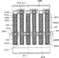
以下,一面参照图1至图36中(B),说明本发明实施例的半导体器件。此外,图1、图3、图5、图7、图9、图11、图13、图15、图17、图19、图21、图23、图27、图29、图31、图33、图35为平面图,但为了进行区域的区别,对一部分标记阴影线。Hereinafter, while referring to FIG. 1 to FIG. 36(B), a semiconductor device according to an embodiment of the present invention will be described. In addition, Figure 1, Figure 3, Figure 5, Figure 7, Figure 9, Figure 11, Figure 13, Figure 15, Figure 17, Figure 19, Figure 21, Figure 23, Figure 27, Figure 29, Figure 31, Figure 33, FIG. 35 is a plan view, but a part is hatched for distinguishing regions.
(第1实施例)(first embodiment)
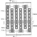
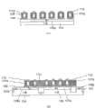
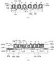
图1、图2中(A)、图2中(B)为显示具有串联连接有本发明实施例1的2段以上的CMOS反向器结合电路的半导体器件。图1为平面图,图2中(A)为图1的切断线A-A’的剖面图,图2中(B)为图1的切断线B-B’的剖面图。1, (A) in FIG. 2, and (B) in FIG. 2 show a semiconductor device having a combination circuit of CMOS inverters having two or more stages connected in series in
以下,参照图1、图2中(A)及图2中(B)说明具备该CMOS反向器结合电路的半导体器件。Hereinafter, a semiconductor device including the CMOS inverter combination circuit will be described with reference to FIGS. 1 , (A) in FIG. 2 , and (B) in FIG. 2 .
在衬底上的NMOS区域形成有N+扩散层106a,在衬底上的PMOS区域形成有P+扩散层107a,N+扩散层106a与P+扩散层107a通过元件分离区域103而分离。N+扩散层106a作为与构成CMOS反向器链的所有的反向器的纵型NMOS晶体管共通的源极扩散区域而发挥功能,P+扩散层107a作为与构成CMOS反向器链的所有的反向器的纵型PMOS晶体管共通的源极扩散区域而发挥功能。The
N+扩散层106a被P阱104所包围,且通过形成在N+扩散层106a的表面的硅化物层115a而连接在邻接于N+扩散层106a而形成的P+扩散层107b。在动作时,对P+扩散层107b,通过配线层施加Vss(通常、接地)电位。因此,对P阱104及N+扩散层106a施加Vss电位。The
同样地,P+扩散层107a被N阱105所包围,且通过邻接在P+扩散层107a而形成的N+扩散层106b与硅化物层115b而连接。在动作时,对N+扩散层106b通过配线层施加Vcc(通常为电源)电位。因此,对N阱105及P+扩散层107a施加Vcc电位。Similarly, the
在N+扩散层106a上形成有构成NMOS的柱状硅层101a,在P+扩散层107a上形成有构成PMOS的多个柱状硅层101b。柱状硅层101a与柱状硅层101b配置成矩阵状。矩阵的同一列(column)的柱状硅层101a与柱状硅层101b配置在大致直线上。同一列的柱状硅层101a与柱状硅层101b构成1段的反向器。此外,矩阵的同一行(row)的柱状硅层101a或柱状硅层101b配置在大致直线上。A
以分别包围柱状硅层101a、101b的方式形成栅极绝缘膜109。此外,以包围各列的(形成1段的反向器)的柱状硅层101a、101b的方式形成有栅极配线111a至111f。A
柱状硅层101a的下端部连接在N+扩散层106a,且形成有N+扩散层,在柱状硅层101a的上端部形成有N+上部扩散层112。柱状硅层101a的下端部的N+扩散层作为源极区域而发挥功能,柱状硅层101a的上端部的N+上部扩散层112作为漏极而发挥功能,源极区域与漏极区域之间的部分作为沟道区域而发挥功能。The lower end of the
柱状硅层101b的下端部连接在P+扩散层107a,且形成有P+扩散层,在柱状硅层101b的上端部形成有P+上部扩散层113。柱状硅层101b的下端部的P+扩散层作为源极区域而发挥功能,柱状硅层101b的上端部的P+上部扩散层113作为漏极而发挥功能,源极区域与漏极区域之间的部分作为沟道区域而发挥功能。栅极配线(栅极电极层)111a至111f包围该沟道区域。如此,形成SGT(Surrounding Gate Transistor,环绕栅极晶体管)。The lower end of the
柱状硅层101a、101b、栅极配线111a至111f、硅化物层115a、115b由绝缘膜117所覆盖。The columnar silicon layers 101 a , 101 b , the
在绝缘膜117形成有:作为各反向器的输入用接触部而发挥功能的栅极配线上接触部121a至121f;及作为输出用接触部而发挥功能的柱状硅层上接触部122、123。Formed on the insulating
栅极配线上接触部121a至121f配置在柱状硅层101a、101b的各列的一侧方,且分别连接在栅极配线111a至111f。输入用接触部121的位置依每列反转。柱状硅层上接触部122隔介NMOS的硅化物层116而连接在柱状硅层101a的上端部所形成的N+上部扩散层112。柱状硅层上接触部123隔介PMOS的硅化物层116而电性连接在柱状硅层101b的上端部所形成的P+上部扩散层113。The
在绝缘膜117的上形成有配线层125(125a至125g)。配线层125a至125g包含:配线层125a,连接在第1段的反向器的栅极配线上接触部121a;配线层125b至125f,将作为各段的反向器的NMOS用输出用接触部而发挥功能的柱状硅层上接触部122、与作为PMOS用输出用接触部而发挥功能的柱状硅层上接触部123彼此连接,并且分别连接在下一段的反向器的栅极配线上接触部121b至121f;及配线层125g,将最终段的反向器的输出用接触部122、123彼此连接且连接在外部电路。A wiring layer 125 ( 125 a to 125 g ) is formed on the insulating
在该种构成中,反向器链的输入电压经由配线层125a与第1段目的反向器的栅极配线上接触部121a而传达至第1段的反向器的栅极配线111a。In this configuration, the input voltage of the inverter chain is transmitted to the gate wiring of the inverter of the first stage through the
第1段的反向器的输出电压输出至连接在形成于柱状硅层101a、101b的N+、P+上部扩散层112、113上的柱状硅层上接触部122、123的配线层125b。该输出电压作为输入电压输入至形成在下一段的反向器的栅极配线111b的端部的栅极配线上接触部121b。The output voltage of the first-stage inverter is output to the
通过反复该基本构成,反向器彼此串联连接。By repeating this basic configuration, the inverters are connected in series.
就本实施例的CMOS反向器的特征而言,所有的反向器使N+扩散层106a及P+扩散层107a共通,在反向器彼此之间并未具备元件分离区域。因此,能以大致最小间隔来配置构成邻接的反向器的柱状硅层。以大致最小间隔来配置构成邻接的反向器的柱状硅层时,一般而言会有输入端子与输出端子的连接困难的问题。在本实施例中,针对该问题,使将施加输入电压的栅极配线的接触部形成在栅极配线的不同侧的端部的反向器交互邻接而配置。借此,可进行第N+1段的反向器的输入端子与第N段的反向器的输出端子的通过配线层的连接。因此,可将串联成2段以上的CMOS反向器达成高集成化。As for the characteristics of the CMOS inverters of this embodiment, all the inverters share the
以下,参照图3至图32中(B),说明图1、图2中(A)、图2中(B)所示的半导体器件的制造方法的一例。在各步骤图中,显示平面图、及平面图所示的切断线A-A’、切断线B-B’的剖面图。Hereinafter, an example of the manufacturing method of the semiconductor device shown in FIG. 1 , FIG. 2 (A) and FIG. 2 (B) will be described with reference to FIGS. 3 to 32 (B). In each step diagram, a plan view and a cross-sectional view along a cutting line A-A' and a cutting line B-B' shown in the plan view are shown.
首先,在硅衬底上形成氮化硅膜等硬掩模(hardmask)层。接着,将硬掩模层予以图案化,使硬掩模层102残留在预定形成柱状硅层的区域。接着,以硬掩模层102为掩模(mask),将衬底的表面区域蚀刻达预定的厚度,如图3、图4中(A)、图4中(B)所示,在衬底上形成硬掩模层102及柱状硅层101a、101b。如前所述,柱状硅层101a构成NMOS,柱状硅层101b构成PMOS。First, a hardmask layer such as a silicon nitride film is formed on a silicon substrate. Next, the hard mask layer is patterned so that the
如图5、图6中(A)、图6中(B)所示,在衬底上将元件分离区域103形成为PMOS区域与NMOS区域的交界区域、各段的反向器的输入用接触部121的预定定形成区域、及该CMOS反向器与周围的交界。元件分离区域103由例如下述的步骤所形成:(1)通过蚀刻等将元件分离用的沟形成在衬底的元件分离区域预定形成区域;(2)通过氧化硅等的涂布或CVD(Chemical VaporDeposition,化学气相沉积)将氧化膜埋入在沟图案;(3)通过干蚀刻或湿蚀刻等将多余的氧化膜予以去除。As shown in Figure 5, (A) in Figure 6, and (B) in Figure 6, the
接着,如图7、图8中(A)、图8中(B)所示,以阻剂(resist)110a覆盖PMOS区域及其侧部,通过离子注入法等将硼等注入在衬底的露出部分,将P阱104形成在NMOS区域与其侧部。Next, as shown in FIG. 7, (A) in FIG. 8, and (B) in FIG. To expose the part, a
接着,去除阻剂110a,以阻剂覆盖NMOS区域及其侧部,并通过离子注入法等将砷等注入在衬底的露出部分,在PMOS区域及其侧部形成N阱105。Next, remove the resist 110a, cover the NMOS region and its sides with the resist, implant arsenic or the like into the exposed portion of the substrate by ion implantation, and form an N well 105 in the PMOS region and its sides.
接着,如图9、图10中(A)、图10中(B)所示,以阻剂110b覆盖PMOS区域及NMOS区域的侧部,并通过离子注入法等将砷等注入在衬底的露出部分。借此,在P阱104形成有N+扩散层106a。此外,也在用以将电位施加至N阱105的扩散层部形成有N+扩散层106b。Next, as shown in FIG. 9 , (A) in FIG. 10 , and (B) in FIG. 10 , the side portions of the PMOS region and the NMOS region are covered with a resist 110b, and arsenic or the like is implanted into the substrate by ion implantation or the like. exposed part. As a result,
接着,去除阻剂110b,以阻剂覆盖NMOS区域、及PMOS区域的侧部,并且通过离子注入法等将硼等注入衬底的露出部分。借此,在N阱105形成有P+扩散层107a。此外,也在用以将电位施加至P阱104的扩散层部形成有P+扩散层107b。Next, the resist 110b is removed, the side portions of the NMOS region and the PMOS region are covered with the resist, and boron or the like is implanted into the exposed portion of the substrate by ion implantation or the like. As a result, the
此外,通过N+扩散层106a中的N型杂质扩散至柱状硅层101a的下端部,而使柱状硅层101a的下端部成为N型。同样地,通过P+扩散层107a中的P型杂质扩散至柱状硅层101b的下端部,而使柱状硅层101b的下端部成为P型。In addition, the lower end portion of the
接着,如图11、图12中(A)、图12中(B)所示,将等离子(plasma)氧化膜等氧化膜成膜在衬底表面。接着,通过以干蚀刻或湿蚀刻对该氧化膜进行回蚀,将用以减低栅极电极与扩散层间的寄生电容的氧化膜108形成在扩散层上。Next, as shown in FIG. 11 , (A) in FIG. 12 , and (B) in FIG. 12 , an oxide film such as a plasma (plasma) oxide film is formed on the surface of the substrate. Next, by etching back the oxide film by dry etching or wet etching, an
接着,如图13、图14中(A)、图14中(B)所示,将栅极绝缘膜109及栅极导电膜111予以成膜。栅极绝缘膜109由氧化硅膜或氮化硅膜等的High-k(高介电率)膜等所形成。硅氧化膜通过例如在氧环境气体中对衬底进行加热,以通过将柱状硅层的表面予以氧化而形成。此外,High-k膜通过例如CVD法而形成。此外,栅极导电膜111由多晶硅膜、金属膜或这些的积层膜所形成。这些的膜通过例如CVD法或溅镀而形成。Next, as shown in FIG. 13 , (A) in FIG. 14 , and (B) in FIG. 14 , a
接着,如图15、图16中(A)、图16中(B)所示,将硬掩模层102作为挡止件(stopper),通过CMP(Chemical Mechanical Polishing,化学机械研磨法)等将栅极导电膜111予以平坦化。Next, as shown in FIG. 15 , (A) in FIG. 16 , and (B) in FIG. 16 , the
接着,如图17、图18中(A)、图18中(B)所示,将栅极导电膜111予以回蚀,将其厚度设定为所希望的栅极长度。Next, as shown in FIG. 17 , (A) in FIG. 18 , and (B) in FIG. 18 , the gate
接着,如图19、图20中(A)、图20中(B)所示,通过湿蚀刻等将硬掩模层102予以去除。Next, as shown in FIG. 19 , (A) in FIG. 20 , and (B) in FIG. 20 , the
接着,如图21、图22中(A)、图22中(B)所示,利用光刻(Lithography)技术等将栅极导电膜111予以图案化,以形成朝柱状硅层的矩阵的列方向延伸的栅极配线111a至111f。Next, as shown in FIG. 21 , (A) in FIG. 22 , and (B) in FIG. 22 , the gate
接着,如图23、图24中(A)、图24中(B)所示,通过离子注入等将砷等注入NMOS区域,而也对柱状硅层101a的上端部注入砷。借此,在柱状硅层101a的上端部形成N+上部扩散层112。同样地,通过离子注入等将氟化硼(BF2)等注入PMOS区域,且在柱状硅层101b的上端部形成P+上部扩散层113。Next, as shown in FIG. 23, FIG. 24(A), and FIG. 24(B), arsenic or the like is implanted into the NMOS region by ion implantation or the like, and arsenic is also implanted into the upper end of the
接着,如图25、图26中(A)、图26中(B)所示,将氧化膜或氮化膜等绝缘膜予以成膜,接着对这些绝缘膜进列回蚀,在柱状硅层101a、101b的上端部(N+上部扩散层112,P+上部扩散层113)的侧壁(露出的侧壁)及栅极配线111a至111f的侧壁(露出的侧壁)形成绝缘膜侧壁114。通过该绝缘膜侧壁114,可防止在后续步骤中形成的硅化物层116的柱状硅层101a,101b的上端部(N+上部扩散层112、P+上部扩散层113)与栅极配线111a至111f的上端部之间的短路、及栅极配线111a至111f的侧壁与形成在衬底的表面区域的扩散层的短路。Next, as shown in Fig. 25, (A) in Fig. 26, and (B) in Fig. 26, an insulating film such as an oxide film or a nitride film is formed, and then these insulating films are etched back, and the columnar silicon layer The side walls (exposed side walls) of the upper ends of 101a and 101b (N+
接着,如图27、图28中(A)、图28中(B)所示,将Co或Ni等金属予以溅镀,然后进行热处理,借此将扩散层(露出部分)选择性予以硅化物(silicide)化,并且在衬底的露出的扩散层上形成硅化物层115a、115b,以在柱状硅层101a及柱状硅层101b的上部形成硅化物层116。Next, as shown in Fig. 27, (A) in Fig. 28, and (B) in Fig. 28, metal such as Co or Ni is sputtered, and then heat treatment is performed to selectively silicide the diffusion layer (exposed part). (silicide) and
接着,如图29、图30中(A)、图30中(B)所示,通过氧化膜等形成层间膜(绝缘膜)117。然后,形成分别连接在栅极配线111a至111f的栅极配线上接触部121a至121f、隔介硅化物层116连接在N+上部扩散层112的柱状硅层上接触部122、及隔介硅化物层116连接在P+上部扩散层113的柱状硅层上接触部123。Next, as shown in FIG. 29 , (A) in FIG. 30 , and (B) in FIG. 30 , an interlayer film (insulating film) 117 is formed by an oxide film or the like. Then, the gate wiring
接着,通过真空蒸镀、溅镀等在衬底整面形成金属膜,将该金属膜予以图案化,如图31、图32中(A)、图32中(B)所示,形成配线层125a至125g。Next, a metal film is formed on the entire surface of the substrate by vacuum evaporation, sputtering, etc., and the metal film is patterned, as shown in Fig. 31, Fig. 32 (A) and Fig. 32 (B), forming
通过以上的步骤,完成具有图1、图2中(A)、图2中(B)所示的构成的,具备结合有至少2段以上的CMOS反向器的CMOS反向器结合电路的半导体器件。Through the above steps, a semiconductor having a structure shown in FIG. 1, (A) in FIG. 2, and (B) in FIG. device.
(第2实施例)(second embodiment)
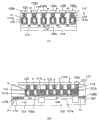
图33、图34中(A)、图34中(B)为显示串联连接成2段以上的CMOS反向器的其他实施例。Fig. 33, (A) in Fig. 34, and (B) in Fig. 34 show other embodiments of CMOS inverters connected in series in two or more stages.
图33为平面图,图34中(A)为图33的平面图的切割线A-A’的剖面图,图34中(B)为图33的平面图的切割线B-B’的剖面图。Fig. 33 is a plan view, among Fig. 34 (A) is the sectional view of the cutting line A-A ' of the plan view of Fig. 33, and among Fig. 34 (B) is the sectional view of the cutting line B-B' of the plan view of Fig. 33.
以下,参照图33及图34中(A)、图34中(B)说明该CMOS反向器。Hereinafter, this CMOS inverter will be described with reference to FIG. 33 , (A) in FIG. 34 , and (B) in FIG. 34 .
在硅制衬底的NMOS区域形成有N+扩散层206a,在PMOS区域形成有P+扩散层207a。N+扩散层206a与P+扩散层207a由元件分离区域203所分离。An
N+扩散层206a由P阱204所包围。此外,N+扩散层206a通过形成在扩散层的表面的硅化物层215a而与邻接N+扩散层206a形成的P+扩散层207b连接。对P+扩散层207b通过配线层施加Vss电位。因此,也对P阱204及N+扩散层206a施加Vss电位。
P+扩散层207a由N阱205所包围。此外,P+扩散层207a通过形成在扩散层的表面的硅化物层215b而与邻接N+扩散层207a形成的N+扩散层206b连接。对N+扩散层206b通过配线层施加Vcc电位。因此,也对N阱205及P+扩散层207a施加Vcc电位。The
在N+扩散层206a的上形成有构成NMOS的柱状硅层201a。此外,在P+扩散层207a的上形成有构成PMOS的柱状硅层201b。A
柱状硅层201a与柱状硅层201b配置成矩阵状。矩阵的同一列的柱状硅层201a与201b配置在大致直线上。各列的柱状硅层201a与柱状硅层201b构成1段的反向器。此外,矩阵的同一行的柱状硅层201a或201b配置在大致直线上。The
以分别包围各柱状硅层201a、201b的方式形成栅极绝缘膜209。此外,以包围各列的(形成1段的反向器)柱状硅层201a、201b的方式形成栅极配线211a至211f。A
在构成NMOS的柱状硅层201a的上端部形成有N+上部扩散层212。在N+上部扩散层212的上形成有硅化物层216。An N+
在构成PMOS的柱状硅层201b的上端部形成有P+上部扩散层213。在P+上部扩散层213的上形成有硅化物层216。A P+
柱状硅层201a、201b、栅极配线211a至211f、硅化物层216由绝缘膜217所覆盖。The columnar silicon layers 201 a , 201 b , the
在绝缘膜217形成有到达栅极配线211a至211f的栅极配线上接触部221a至221f、及电性连接至各柱状硅层201a,201b的柱状硅层上接触部222、223。关于奇数段的反向器,栅极配线上接触部221配置在区分PMOS区域与NMOS区域的元件分离区域203的上,关于偶数段的反向器,栅极配线上接触部221配置在柱状硅层的列的两侧。On the insulating
在绝缘膜217的上形成有配线层225(225a至225j)。A wiring layer 225 ( 225 a to 225 j ) is formed on the insulating
配线层225包含:连接在第1段反向器的栅极配线上接触部221a的配线层225a;将奇数段的反向器的柱状硅层上接触部223彼此连接,并且连接在下一段的反向器的栅极配线上接触部221b的配线层225b、225c;将奇数段的反向器的柱状硅层上接触部222彼此连接,并且连接在下一段的反向器的栅极配线上接触部221c的配线层225c;及将偶数段的反向器的柱状硅层上接触部222彼此连接,并且连接在下一段的反向器的元件分离区域203上的栅极配线上接触部221d的配线层225d。The
在该构成中,反向器链的输入电压经由配线层225a与栅极配线上接触部221a传达至第1段的反向器的栅极配线211a。In this configuration, the input voltage of the inverter chain is transmitted to the
第1段的反向器的输出电压输出至连接有形成在柱状硅层201a的N+上部扩散层212上的柱状硅层上接触部222的配线层225c、及连接有形成在柱状硅层201b的P+上部扩散层213上的柱状硅层上接触部223的配线层225b。该输出电压作为输入电压分别输入至形成在下一段的反向器的栅极配线211b的两端部的栅极配线上接触部221c、221b。The output voltage of the inverter of the first stage is output to the
之后,反复进行同样的动作。第6段的反向器的输出成为该CMOS反向器结合电路的输出。Thereafter, the same operation is repeated. The output of the inverter in the sixth stage becomes the output of the CMOS inverter combination circuit.
就本实施例的特征而言,所有的反向器共同具有N+扩散层206a及P+扩散层207a。因此,无须在反向器之间形成元件分离。因此,能以大致最小间隔来配置构成邻接的反向器的柱状硅层。以大致最小间隔来配置构成邻接的反向器的柱状硅层时,一般而言会有输入端子与输出端子的通过配线层的连接困难的问题。然而,在本实施例中,通过交互邻接配置具有施加输入电压的栅极配线上接触部221a,且形成在NMOS区域与PMOS区域之间的反向器、及具有施加输入电压的栅极配线上接触部221b、221c,且形成在栅极配线的两端的反向器,而可容易地进行输入端子与输出端子的通过配线层的连接。因此,可使串联成2段以上的CMOS反向器达成高集成化。In terms of the characteristics of this embodiment, all the inverters have the
在本实施例中,来自构成NMOS的柱状硅层201a上部的漏极扩散层的输出输出至配线层225c、225f、225i,来自构成PMOS的柱状硅层201b上部的漏极扩散层的输出为输出至配线层225b、225e、225h,且分别输入至下一段的栅极配线。本发明并不限定于此,如图35、图36中(A)、图36中(B)所示,接触部可将配线层225b、225e、225h与配线层225C、225f、225i分别直接连接在上层配线层227、及通过使用配线层上接触部226而连接在上层配线层227。此情形时,无须从形成在栅极的两端的接触部来进行对下一段的栅极的输入,如图35、图36中(A)、图36中(B)所示,也可仅在栅极的单侧的端部形成接触部。In this embodiment, the output from the drain diffusion layer above the
在所述实施例中,虽例示使用硅的例作为半导体,但若可形成纵型MOS晶体管,则也可使用锗、化合物半导体等。In the above-described embodiments, an example of using silicon as a semiconductor was exemplified, but if a vertical MOS transistor can be formed, germanium, a compound semiconductor, or the like may be used.
上述的物质名为例示,并非被限定。The above-mentioned substances are only examples and are not intended to be limited.
此外,本发明在不脱离本发明的广义精神与范围的情形下,可进行各种实施例及变形。并且,上述实施例为用以说明本发明的一实施例,并非限定本发明的范围。In addition, various embodiments and modifications can be made to the present invention without departing from the broad spirit and scope of the present invention. In addition, the above-mentioned embodiment is an embodiment for illustrating the present invention, and does not limit the scope of the present invention.
Claims (4)
Translated fromChineseApplications Claiming Priority (2)
| Application Number | Priority Date | Filing Date | Title |
|---|---|---|---|
| JP2010-097735 | 2010-04-21 | ||
| JP2010097735AJP5128630B2 (en) | 2010-04-21 | 2010-04-21 | Semiconductor device |
Publications (2)
| Publication Number | Publication Date |
|---|---|
| CN102237359Atrue CN102237359A (en) | 2011-11-09 |
| CN102237359B CN102237359B (en) | 2013-06-05 |
Family
ID=44815079
Family Applications (1)
| Application Number | Title | Priority Date | Filing Date |
|---|---|---|---|
| CN2011101044183AExpired - Fee RelatedCN102237359B (en) | 2010-04-21 | 2011-04-21 | Semiconductor device |
Country Status (5)
| Country | Link |
|---|---|
| US (1) | US8319288B2 (en) |
| JP (1) | JP5128630B2 (en) |
| KR (1) | KR101173452B1 (en) |
| CN (1) | CN102237359B (en) |
| TW (1) | TW201138065A (en) |
Cited By (2)
| Publication number | Priority date | Publication date | Assignee | Title |
|---|---|---|---|---|
| CN103928458A (en)* | 2013-01-15 | 2014-07-16 | 阿尔特拉公司 | metal programmable integrated circuit |
| CN105473990A (en)* | 2013-08-22 | 2016-04-06 | 株式会社电装 | Load sensor using vertical transistor |
Families Citing this family (19)
| Publication number | Priority date | Publication date | Assignee | Title |
|---|---|---|---|---|
| JP4487221B1 (en)* | 2009-04-17 | 2010-06-23 | 日本ユニサンティスエレクトロニクス株式会社 | Semiconductor device |
| US8877578B2 (en) | 2012-05-18 | 2014-11-04 | Unisantis Electronics Singapore Pte. Ltd. | Method for producing semiconductor device and semiconductor device |
| US8697511B2 (en) | 2012-05-18 | 2014-04-15 | Unisantis Electronics Singapore Pte. Ltd. | Method for producing semiconductor device and semiconductor device |
| US8742492B2 (en)* | 2012-08-07 | 2014-06-03 | Taiwan Semiconductor Manufacturing Company, Ltd. | Device with a vertical gate structure |
| US9764950B2 (en)* | 2013-08-16 | 2017-09-19 | Taiwan Semiconductor Manufacturing Company Limited | Semiconductor arrangement with one or more semiconductor columns |
| WO2015155863A1 (en)* | 2014-04-10 | 2015-10-15 | ユニサンティス エレクトロニクス シンガポール プライベート リミテッド | Semiconductor device |
| US10026658B2 (en)* | 2014-04-14 | 2018-07-17 | Taiwan Semiconductor Manufacturing Company Limited | Methods for fabricating vertical-gate-all-around transistor structures |
| JP6667215B2 (en)* | 2014-07-24 | 2020-03-18 | キヤノン株式会社 | X-ray shielding grating, structure, Talbot interferometer, and method of manufacturing X-ray shielding grating |
| JP5986618B2 (en)* | 2014-12-04 | 2016-09-06 | ユニサンティス エレクトロニクス シンガポール プライベート リミテッドUnisantis Electronics Singapore Pte Ltd. | Semiconductor device |
| US10026653B2 (en)* | 2015-12-16 | 2018-07-17 | International Business Machines Corporation | Variable gate lengths for vertical transistors |
| US11251179B2 (en) | 2016-06-30 | 2022-02-15 | International Business Machines Corporation | Long channel and short channel vertical FET co-integration for vertical FET VTFET |
| US9761712B1 (en)* | 2016-10-31 | 2017-09-12 | International Business Machines Corporation | Vertical transistors with merged active area regions |
| US10672888B2 (en) | 2017-08-21 | 2020-06-02 | International Business Machines Corporation | Vertical transistors having improved gate length control |
| WO2019116883A1 (en)* | 2017-12-12 | 2019-06-20 | 株式会社ソシオネクスト | Semiconductor integrated circuit device |
| US10410925B2 (en)* | 2017-12-29 | 2019-09-10 | Micron Technology, Inc. | Methods of forming integrated assemblies |
| US10381355B2 (en)* | 2018-01-11 | 2019-08-13 | International Business Machines Corporation | Dense vertical field effect transistor structure |
| KR102059896B1 (en)* | 2018-10-24 | 2019-12-27 | 가천대학교 산학협력단 | One-transistor dram cell device having quantum well structure |
| CN115249691A (en)* | 2022-07-25 | 2022-10-28 | 长江存储科技有限责任公司 | Semiconductor test structure, manufacturing method and test method thereof, and semiconductor device |
| TWI854564B (en)* | 2023-03-30 | 2024-09-01 | 華邦電子股份有限公司 | Semiconductor device and method forming the same |
Citations (4)
| Publication number | Priority date | Publication date | Assignee | Title |
|---|---|---|---|---|
| US5258635A (en)* | 1988-09-06 | 1993-11-02 | Kabushiki Kaisha Toshiba | MOS-type semiconductor integrated circuit device |
| US20040262681A1 (en)* | 2003-05-28 | 2004-12-30 | Fujio Masuoka | Semiconductor device |
| WO2009016880A1 (en)* | 2007-08-02 | 2009-02-05 | Unisantis Electronics (Japan) Ltd. | Semiconductor device |
| CN101542715A (en)* | 2007-05-30 | 2009-09-23 | 日本优尼山帝斯电子股份有限公司 | Semiconductor device |
Family Cites Families (5)
| Publication number | Priority date | Publication date | Assignee | Title |
|---|---|---|---|---|
| JP2703970B2 (en) | 1989-01-17 | 1998-01-26 | 株式会社東芝 | MOS type semiconductor device |
| JP5460950B2 (en)* | 2007-06-06 | 2014-04-02 | ピーエスフォー ルクスコ エスエイアールエル | Semiconductor device and manufacturing method thereof |
| US8212298B2 (en)* | 2008-01-29 | 2012-07-03 | Unisantis Electronics Singapore Pte Ltd. | Semiconductor storage device and methods of producing it |
| JP4316657B2 (en) | 2008-01-29 | 2009-08-19 | 日本ユニサンティスエレクトロニクス株式会社 | Semiconductor device |
| JP4487221B1 (en)* | 2009-04-17 | 2010-06-23 | 日本ユニサンティスエレクトロニクス株式会社 | Semiconductor device |
- 2010
- 2010-04-21JPJP2010097735Apatent/JP5128630B2/enactiveActive
- 2011
- 2011-03-28KRKR1020110027412Apatent/KR101173452B1/enactiveActive
- 2011-04-12TWTW100112627Apatent/TW201138065A/enunknown
- 2011-04-20USUS13/090,726patent/US8319288B2/enactiveActive
- 2011-04-21CNCN2011101044183Apatent/CN102237359B/ennot_activeExpired - Fee Related
Patent Citations (4)
| Publication number | Priority date | Publication date | Assignee | Title |
|---|---|---|---|---|
| US5258635A (en)* | 1988-09-06 | 1993-11-02 | Kabushiki Kaisha Toshiba | MOS-type semiconductor integrated circuit device |
| US20040262681A1 (en)* | 2003-05-28 | 2004-12-30 | Fujio Masuoka | Semiconductor device |
| CN101542715A (en)* | 2007-05-30 | 2009-09-23 | 日本优尼山帝斯电子股份有限公司 | Semiconductor device |
| WO2009016880A1 (en)* | 2007-08-02 | 2009-02-05 | Unisantis Electronics (Japan) Ltd. | Semiconductor device |
Cited By (3)
| Publication number | Priority date | Publication date | Assignee | Title |
|---|---|---|---|---|
| CN103928458A (en)* | 2013-01-15 | 2014-07-16 | 阿尔特拉公司 | metal programmable integrated circuit |
| CN105473990A (en)* | 2013-08-22 | 2016-04-06 | 株式会社电装 | Load sensor using vertical transistor |
| CN105473990B (en)* | 2013-08-22 | 2018-12-18 | 株式会社电装 | Use the load transducer of vertical access transistor |
Also Published As
| Publication number | Publication date |
|---|---|
| US8319288B2 (en) | 2012-11-27 |
| JP5128630B2 (en) | 2013-01-23 |
| CN102237359B (en) | 2013-06-05 |
| JP2011228519A (en) | 2011-11-10 |
| TW201138065A (en) | 2011-11-01 |
| KR20110117605A (en) | 2011-10-27 |
| KR101173452B1 (en) | 2012-08-13 |
| US20110260259A1 (en) | 2011-10-27 |
Similar Documents
| Publication | Publication Date | Title |
|---|---|---|
| CN102237359B (en) | Semiconductor device | |
| US8212311B2 (en) | Semiconductor device having increased gate length implemented by surround gate transistor arrangements | |
| CN101542715B (en) | Semiconductor device | |
| JP4030383B2 (en) | Semiconductor device and manufacturing method thereof | |
| KR101128117B1 (en) | Semiconductor device | |
| US7112858B2 (en) | Semiconductor device and manufacturing method of the same | |
| CN111418063A (en) | Non-volatile split gate memory cell with integrated high-K metal control gate and method of manufacture | |
| US10818800B2 (en) | Semiconductor structure and method for preparing the same | |
| CN1933157A (en) | Semiconductor device and a method of manufacturing the same | |
| WO2018033981A1 (en) | Column-shaped semiconductor device, and method for manufacturing same | |
| US20160027778A1 (en) | Semiconductor device | |
| US20060091474A1 (en) | Semiconductor device and manufacturing method thereof | |
| US8067283B2 (en) | Semiconductor device fabricating method | |
| US7468540B2 (en) | Semiconductor device and method for manufacturing the same | |
| US6597043B1 (en) | Narrow high performance MOSFET device design | |
| US20020096712A1 (en) | Semiconductor device and method for manufacturing the same | |
| TWI239596B (en) | Semiconductor device and method of manufacturing the same | |
| CN111477590B (en) | Grid manufacturing method | |
| JP2006179635A (en) | CMOS semiconductor device | |
| JP4015086B2 (en) | Manufacturing method of semiconductor device | |
| WO2015083273A1 (en) | Semiconductor device and manufacturing method for same | |
| JP3259439B2 (en) | Method for manufacturing semiconductor device | |
| CN115207126A (en) | MOSFET structure and manufacturing method thereof | |
| JP2007311694A (en) | Semiconductor device | |
| JPS63310173A (en) | Semiconductor device and its manufacture |
Legal Events
| Date | Code | Title | Description |
|---|---|---|---|
| C06 | Publication | ||
| PB01 | Publication | ||
| C10 | Entry into substantive examination | ||
| SE01 | Entry into force of request for substantive examination | ||
| ASS | Succession or assignment of patent right | Owner name:UNISANTIS ELECTRONICS SINGAPORE PTE. LTD. Free format text:FORMER OWNER: UNISANTIS ELECTRONICS JAPAN LIMITED Effective date:20111121 | |
| C41 | Transfer of patent application or patent right or utility model | ||
| TA01 | Transfer of patent application right | Effective date of registration:20111121 Address after:Peninsular Plaza, Singapore Applicant after:Unisantis Electronics Singapore Pte. Ltd. Address before:Tokyo, Japan Applicant before:Unisantis Electronics Singapore Pte. Ltd. | |
| C14 | Grant of patent or utility model | ||
| GR01 | Patent grant | ||
| CF01 | Termination of patent right due to non-payment of annual fee | ||
| CF01 | Termination of patent right due to non-payment of annual fee | Granted publication date:20130605 |