CN102236480A - Projection type capacitive touch screen - Google Patents
Projection type capacitive touch screenDownload PDFInfo
- Publication number
- CN102236480A CN102236480ACN2010101602876ACN201010160287ACN102236480ACN 102236480 ACN102236480 ACN 102236480ACN 2010101602876 ACN2010101602876 ACN 2010101602876ACN 201010160287 ACN201010160287 ACN 201010160287ACN 102236480 ACN102236480 ACN 102236480A
- Authority
- CN
- China
- Prior art keywords
- layer
- electrode
- touch screen
- capacitive touch
- transparent
- Prior art date
- Legal status (The legal status is an assumption and is not a legal conclusion. Google has not performed a legal analysis and makes no representation as to the accuracy of the status listed.)
- Pending
Links
Images


Landscapes
- Position Input By Displaying (AREA)
Abstract
Translated fromChinese
Description
Translated fromChinese技术领域technical field
本发明属于触摸屏领域,尤其涉及一种投射式电容触摸屏。The invention belongs to the field of touch screens, in particular to a projected capacitive touch screen.
背景技术Background technique
触摸屏种类繁多,可以分为电阻式、电容式、红外线式和表面声波式。其中,电容式触摸屏是利用触摸表面与人体之间的静电结合产生电容变化,从产生的诱导电流来检测其坐标。电容式触摸屏可分为投射电容式触摸屏和表面电容式触摸屏,投射电容式触摸屏是通过准确测定触摸点沿水平轴和垂直轴触摸的位置,来获得很高的触摸精度,且支持多点触控,主要用于手机产品中;表面电容式触摸屏是通过将未知电容上的电荷转移,然后测量电荷的多少,从而确定未知电容的大小,一般是单点触控,稳定性较差,主要用于大型公共查询设备中。其中,投射电容式触摸屏的传感器可以采用单层电极结构,这种结构的触摸屏由于触摸灵敏度高,耐用性好,能有效防止外部环境因素对触摸屏的影响,支持多点触控操作,并且透过率和分辨率均具有良好表现,因而得到广泛应用。There are many types of touch screens, which can be divided into resistive, capacitive, infrared and surface acoustic wave. Among them, the capacitive touch screen uses the electrostatic combination between the touch surface and the human body to generate capacitance changes, and detects its coordinates from the induced current generated. Capacitive touch screens can be divided into projected capacitive touch screens and surface capacitive touch screens. Projected capacitive touch screens obtain high touch accuracy by accurately measuring the position of touch points along the horizontal and vertical axes, and support multi-touch , mainly used in mobile phone products; the surface capacitive touch screen is to determine the size of the unknown capacitance by transferring the charge on the unknown capacitor and then measuring the charge. Generally, it is a single-point touch with poor stability and is mainly used In a large public query facility. Among them, the sensor of the projected capacitive touch screen can adopt a single-layer electrode structure. The touch screen with this structure has high touch sensitivity and good durability, which can effectively prevent the influence of external environmental factors on the touch screen, support multi-touch operation, and pass through It has good performance in both rate and resolution, so it is widely used.
在现有技术中,投射式电容触摸屏的构造主要分为两层,分别为:含有装饰层的上层保护基板,以及镀有铟锡氧化物(Indium Tin Oxides,简称ITO)电极层和连接金属引线的下层导电基板。其中,含有装饰层的上层保护基板用于保护下层导电基板,同时将下层导电基板上不透明的金属引线进行遮挡,这种电容式触摸屏的缺点是结构复杂,制作成本高。具体地,在制作时,需要将上层保护基板与下层导电基板通过粘结剂粘合在一起,常用的粘接方法有:用固态光学双面胶将上、下基板粘结并贴合在一起,这种贴合方法的主要缺陷是贴合过程中容易产生气泡,且残留的气泡很难消除;或者用点胶贴合机将紫外线固化胶或加热固化胶,涂敷在上、下基板上并贴合在一起,这种方法的主要缺陷是贴合过程中多余的胶水会沿着基板四周溢出,比较难以处理。In the prior art, the structure of the projected capacitive touch screen is mainly divided into two layers, namely: an upper protective substrate containing a decorative layer, and an electrode layer coated with indium tin oxide (Indium Tin Oxides, referred to as ITO) and connecting metal leads. the underlying conductive substrate. Wherein, the upper protective substrate containing the decorative layer is used to protect the lower conductive substrate, and at the same time shield the opaque metal leads on the lower conductive substrate. The disadvantage of this capacitive touch screen is that the structure is complex and the production cost is high. Specifically, during production, the upper protective substrate and the lower conductive substrate need to be bonded together with an adhesive. Commonly used bonding methods include: bonding and pasting the upper and lower substrates together with solid optical double-sided adhesive , the main defect of this laminating method is that air bubbles are easy to be generated during the laminating process, and the residual air bubbles are difficult to eliminate; or use a dispensing laminating machine to apply ultraviolet curable glue or heat curable glue on the upper and lower substrates And fit together, the main defect of this method is that the excess glue will overflow along the periphery of the substrate during the bonding process, which is difficult to handle.
发明内容Contents of the invention
本发明为解决现有投射式电容触摸屏中需要起装饰和保护作用的上层保护基板而造成的制作成本较高,同时由于贴合而造成的良率降低的技术问题,提供一种投射式电容式触摸屏,所述投射式电容式触摸屏结构简单、成本较低、良率较高。The present invention provides a projected capacitive touch screen in order to solve the technical problem of high production cost caused by the upper protective substrate that needs to play a decorative and protective role in the existing projected capacitive touch screen, and at the same time, the yield rate is reduced due to lamination. For a touch screen, the projected capacitive touch screen has a simple structure, low cost and high yield.
本发明是通过以下技术方案来实现的:The present invention is achieved through the following technical solutions:
一种投射式电容触摸屏,包括透明基板;配置于所述透明基板一面的透明电极层,所述透明电极层由水平和垂直两组电极组成;在透明基板上、围绕透明电极层的周边缘设置的绝缘装饰层,所述绝缘装饰层上设置有多个通孔,通孔与电极的电极端一一相对;在绝缘装饰层与透明基板相背的一面设置的边缘金属引线,边缘金属引线通过绝缘装饰层上设置的通孔与电极的电极端连接;覆盖于透明电极层、绝缘装饰层和边缘金属引线表面的绝缘保护层。A projected capacitive touch screen, comprising a transparent substrate; a transparent electrode layer arranged on one side of the transparent substrate, the transparent electrode layer is composed of two sets of electrodes, horizontal and vertical; on the transparent substrate, arranged around the peripheral edge of the transparent electrode layer The insulating decorative layer is provided with a plurality of through holes, and the through holes are opposite to the electrode ends of the electrodes; the edge metal leads are arranged on the side opposite to the transparent substrate, and the edge metal leads pass through The through hole provided on the insulating decoration layer is connected with the electrode end of the electrode; the insulating protection layer covers the surface of the transparent electrode layer, the insulating decoration layer and the edge metal leads.
本发明提供的投射式电容触摸屏,将现有电容式触摸屏的双层透明基板结构改变成单层透明基板结构,结构简单,且在保持投射式电容触摸屏的所有功能的前提下,通过在与透明电极层同面的透明基板上制作出绝缘装饰层,使所述投射式电容触摸屏节省了上层保护基板、以及制作中将上层保护基板与下层导电基板的贴合工序,节省了成本,避免由于所述的贴合工序造成的不良,提高了产品的良率。The projected capacitive touch screen provided by the present invention changes the double-layer transparent substrate structure of the existing capacitive touch screen into a single-layer transparent substrate structure, has a simple structure, and maintains all functions of the projected capacitive touch screen. An insulating decorative layer is made on the transparent substrate on the same surface as the electrode layer, so that the projected capacitive touch screen saves the upper protective substrate and the bonding process of the upper protective substrate and the lower conductive substrate during production, which saves costs and avoids The defects caused by the bonding process mentioned above can improve the yield rate of the product.
附图说明Description of drawings
图1是本发明实施例提供的投射式电容触摸屏结构示意图;FIG. 1 is a schematic structural diagram of a projected capacitive touch screen provided by an embodiment of the present invention;
图2是本发明实施例提供的边缘金属引线与透明电极连接方式示意图;Fig. 2 is a schematic diagram of the connection method between the edge metal lead and the transparent electrode provided by the embodiment of the present invention;
图3是图1中投射式电容触摸屏的展开结构示意图;Fig. 3 is a schematic diagram of the unfolded structure of the projected capacitive touch screen in Fig. 1;
图4是图3中边缘金属引线的局部放大示意图;Fig. 4 is a partially enlarged schematic diagram of the edge metal leads in Fig. 3;
图5是图3中绝缘装饰层的局部放大示意图;Fig. 5 is a partially enlarged schematic diagram of the insulating decorative layer in Fig. 3;
图6是图3中透明电极层的局部放大示意图。FIG. 6 is a partially enlarged schematic view of the transparent electrode layer in FIG. 3 .
具体实施方式Detailed ways
为了使本发明所解决的技术问题、技术方案及有益效果更加清楚明白,以下结合附图及实施例,对本发明进行进一步详细说明。应当理解,此处所描述的具体实施例仅仅用以解释本发明,并不用于限定本发明。In order to make the technical problems, technical solutions and beneficial effects solved by the present invention clearer, the present invention will be further described in detail below in conjunction with the accompanying drawings and embodiments. It should be understood that the specific embodiments described here are only used to explain the present invention, not to limit the present invention.
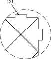
请参考图1至图6所示,一种投射式电容触摸屏,包括透明基板11;配置于所述透明基板一面的透明电极层12,所述透明电极层由水平和垂直两组电极组成;在透明基板上、围绕透明电极层的周边缘设置的绝缘装饰层13,所述绝缘装饰层上设置有多个通孔131,在所述通孔的位置处,透明电极层中各个电极的电极端121部分露出,通孔与电极的电极端一一相对;在绝缘装饰层与透明基板相背的一面设置的边缘金属引线14,边缘金属引线通过绝缘装饰层上设置的通孔与通孔处露出的电极端121连接;覆盖于透明电极层、绝缘装饰层和边缘金属引线表面的绝缘保护层15。Please refer to FIG. 1 to FIG. 6, a projected capacitive touch screen includes a
本发明中,所述透明基板11由光学透明绝缘材料构成,所述光学透明绝缘材料可以是硅酸盐玻璃、树脂类刚性透明绝缘材料,例如聚甲基丙烯酸甲酯(PMMA)、聚碳酸酯(PC)。In the present invention, the
所述绝缘透明基板11的一个表面上,配有透明电极层12,所述透明电极层12可通过真空磁控溅射法将透明导电材料镀在绝缘透明基板11上,所述透明电极层12由透明导电材料构成,所述透明导电材料可以是氧化铟锡(ITO)、掺杂铝的氧化锌(AZO)、掺杂铟的氧化锌(IZO)、掺杂镓的氧化锌、掺杂锑的氧化锡、掺杂锌的氧化锡或者其他透明导电材料。One surface of the insulating
所述透明电极层12由水平和垂直两组电极组成,所述两组电极中第一组电极的单个电极单元连续设置,第二组电极的单个电极单元以第一组电极的单个电极单元为间隔分段设置。作为一种具体实施方式,假定第一组电极为水平电极,所述第一组电极包括多条水平电极;第二组电极则为垂直电极,所述第二组电极包括多条垂直电极,每一条水平电极和垂直电极都由多个电极单元构成。因此,由前述可知,所述水平电极的单个电极单元连续设置,垂直电极的单个电极单元以水平电极的单个电极单元为间隔分段设置。具体地,包括对应于所述垂直电极、且附着在所述透明基板11上分段设置的透明导电膜,附着在所述透明导电膜中部和邻近的透明基板上的绝缘膜,所述水平电极横跨所述透明导电膜附着在所述绝缘膜和透明基板上,位于所述水平电极两侧的垂直电极覆盖在所述透明导电膜端部和所述透明基板上,构成第二组电极。The
当然,所述透明电极层12中水平和垂直电极的构成方式还很多种,本领域的技术人员在前述具体实施方式的基础上可以作若干的变化,比如所述两组电极中第二组电极的单个电极单元连续设置,第一组电极的单个电极单元以第二组电极的单个电极单元为间隔分段设置,等等其它方式,在此不再赘述。Of course, there are many ways to form the horizontal and vertical electrodes in the
在透明基板上、围绕透明电极层的周边缘设置有绝缘装饰层13,所述绝缘装饰层的材料可选择为分散型树脂类颜料、聚酯类颜料、聚碳酸类树脂类颜料;优选为分散型树脂类颜料,并采用光刻法或者喷墨法制作。所述绝缘装饰层上设置有多个通孔131,所述通孔为微米级的通孔,由于边缘金属引线电极的线宽为微米级的,因此,设计的通孔同样为微米级。在所述通孔的位置处,透明电极层12中各个电极的电极端121部分露出,其通孔131与电极的电极端121一一相对。On the transparent substrate, an insulating
绝缘装饰层与透明基板相背的一面设置有边缘金属引线14,边缘金属引线端141通过绝缘装饰层上设置的通孔与通孔处露出的电极端121连接,实现信号的传递,由此每一条透明导电电极都由所述边缘金属引线14引出,连接至柔性印刷线路板(FPC),并由电容式感应芯片来驱动。该芯片既能将数据传送到一个主处理器,也能自己处理触摸点的水平和垂直位置,并独立在整个屏幕上跟踪每个触摸点,达到多点触摸的特性。所述边缘金属引线的材料选自钼(Mo)、铝(Al)、铜(Cu)、铬(Cr)、银(Ag)、金(Au)中的至少一种,采用磁控溅射法制作;或者,所述边缘金属引线由银浆构成,采用丝网印刷制作。The side of the insulating decoration layer opposite to the transparent substrate is provided with an
覆盖于透明电极层、绝缘装饰层和边缘金属引线表面的绝缘保护层15,即所绝缘保护层15完全将透明电极层12、绝缘装饰层13和边缘金属引线14覆盖。所述绝缘保护层15由透明绝缘材料构成,可选自二氧化硅(SiO2)和环氧树脂类有机玻璃中的任一种或者其他透明绝缘材料。The
本发明提供的投射式电容触摸屏,将现有电容式触摸屏的双层透明基板结构改变成单层透明基板结构,结构简单,且在保持投射式电容触摸屏的所有功能的前提下,通过在与透明电极层同面的透明基板上制作出绝缘装饰层,使所述投射式电容触摸屏节省了上层保护基板、以及制作中将上层保护基板与下层导电基板的贴合工序,节省了成本,避免由于所述的贴合工序造成的不良,提高了产品的良率。The projected capacitive touch screen provided by the present invention changes the double-layer transparent substrate structure of the existing capacitive touch screen into a single-layer transparent substrate structure, has a simple structure, and maintains all functions of the projected capacitive touch screen. An insulating decorative layer is made on the transparent substrate on the same surface as the electrode layer, so that the projected capacitive touch screen saves the upper protective substrate and the bonding process of the upper protective substrate and the lower conductive substrate during production, which saves costs and avoids The defects caused by the bonding process mentioned above can improve the yield rate of the product.
以上所述仅为本发明的较佳实施例而已,并不用以限制本发明,凡在本发明的精神和原则之内所作的任何修改、等同替换和改进等,均应包含在本发明的保护范围之内。The above descriptions are only preferred embodiments of the present invention, and are not intended to limit the present invention. Any modifications, equivalent replacements and improvements made within the spirit and principles of the present invention should be included in the protection of the present invention. within range.
Claims (6)
Priority Applications (1)
| Application Number | Priority Date | Filing Date | Title |
|---|---|---|---|
| CN2010101602876ACN102236480A (en) | 2010-04-23 | 2010-04-23 | Projection type capacitive touch screen |
Applications Claiming Priority (1)
| Application Number | Priority Date | Filing Date | Title |
|---|---|---|---|
| CN2010101602876ACN102236480A (en) | 2010-04-23 | 2010-04-23 | Projection type capacitive touch screen |
Publications (1)
| Publication Number | Publication Date |
|---|---|
| CN102236480Atrue CN102236480A (en) | 2011-11-09 |
Family
ID=44887181
Family Applications (1)
| Application Number | Title | Priority Date | Filing Date |
|---|---|---|---|
| CN2010101602876APendingCN102236480A (en) | 2010-04-23 | 2010-04-23 | Projection type capacitive touch screen |
Country Status (1)
| Country | Link |
|---|---|
| CN (1) | CN102236480A (en) |
Cited By (8)
| Publication number | Priority date | Publication date | Assignee | Title |
|---|---|---|---|---|
| CN102662546A (en)* | 2012-04-09 | 2012-09-12 | 福建连城天域高科技有限公司 | Projection type capacitive touch screen |
| CN103207704A (en)* | 2013-04-16 | 2013-07-17 | 南昌欧菲光显示技术有限公司 | Touch panel and production method thereof |
| CN103530008A (en)* | 2013-09-24 | 2014-01-22 | 昆山鑫宏达电子科技有限公司 | Capacitive touch screen |
| CN103677459A (en)* | 2012-09-25 | 2014-03-26 | 比亚迪股份有限公司 | Capacitive touch screen and manufacturing method thereof |
| WO2014117728A1 (en)* | 2013-01-30 | 2014-08-07 | 福建科创光电有限公司 | One glass solution capacitive touch screen and manufacturing method thereof |
| CN104571671A (en)* | 2013-10-14 | 2015-04-29 | 明兴光电股份有限公司 | Touch panel |
| CN105103096A (en)* | 2013-03-18 | 2015-11-25 | 富士胶片株式会社 | Touch panel and resin composition for forming protective layer |
| CN107340943A (en)* | 2017-09-14 | 2017-11-10 | 长沙市宇顺显示技术有限公司 | A kind of capacitive touch screen and its applying method |
Citations (4)
| Publication number | Priority date | Publication date | Assignee | Title |
|---|---|---|---|---|
| CN101038525A (en)* | 2006-03-15 | 2007-09-19 | 胜华科技股份有限公司 | Resistive touch panel manufacturing method |
| CN201078769Y (en)* | 2007-04-27 | 2008-06-25 | 宸鸿光电科技股份有限公司 | Touch pattern structure of capacitive touch pad |
| CN101414067A (en)* | 2007-10-19 | 2009-04-22 | 统宝光电股份有限公司 | Image display system and related touch sensing circuit |
| CN101609384A (en)* | 2008-06-18 | 2009-12-23 | 爱普生映像元器件有限公司 | Capacitive input device and display device with input function |
- 2010
- 2010-04-23CNCN2010101602876Apatent/CN102236480A/enactivePending
Patent Citations (4)
| Publication number | Priority date | Publication date | Assignee | Title |
|---|---|---|---|---|
| CN101038525A (en)* | 2006-03-15 | 2007-09-19 | 胜华科技股份有限公司 | Resistive touch panel manufacturing method |
| CN201078769Y (en)* | 2007-04-27 | 2008-06-25 | 宸鸿光电科技股份有限公司 | Touch pattern structure of capacitive touch pad |
| CN101414067A (en)* | 2007-10-19 | 2009-04-22 | 统宝光电股份有限公司 | Image display system and related touch sensing circuit |
| CN101609384A (en)* | 2008-06-18 | 2009-12-23 | 爱普生映像元器件有限公司 | Capacitive input device and display device with input function |
Cited By (12)
| Publication number | Priority date | Publication date | Assignee | Title |
|---|---|---|---|---|
| CN102662546A (en)* | 2012-04-09 | 2012-09-12 | 福建连城天域高科技有限公司 | Projection type capacitive touch screen |
| CN103677459A (en)* | 2012-09-25 | 2014-03-26 | 比亚迪股份有限公司 | Capacitive touch screen and manufacturing method thereof |
| WO2014117728A1 (en)* | 2013-01-30 | 2014-08-07 | 福建科创光电有限公司 | One glass solution capacitive touch screen and manufacturing method thereof |
| CN104956298A (en)* | 2013-01-30 | 2015-09-30 | 福建科创光电有限公司 | One glass solution capacitive touch screen and manufacturing method thereof |
| US9760227B2 (en) | 2013-01-30 | 2017-09-12 | Fujian Kechuang Photoelectric Co., Ltd. | OGS captive touch panel and method for manufacturing same |
| CN105103096A (en)* | 2013-03-18 | 2015-11-25 | 富士胶片株式会社 | Touch panel and resin composition for forming protective layer |
| CN103207704A (en)* | 2013-04-16 | 2013-07-17 | 南昌欧菲光显示技术有限公司 | Touch panel and production method thereof |
| CN103207704B (en)* | 2013-04-16 | 2016-04-27 | 南昌欧菲光显示技术有限公司 | Contact panel and manufacture method thereof |
| CN103530008A (en)* | 2013-09-24 | 2014-01-22 | 昆山鑫宏达电子科技有限公司 | Capacitive touch screen |
| CN104571671A (en)* | 2013-10-14 | 2015-04-29 | 明兴光电股份有限公司 | Touch panel |
| CN107340943A (en)* | 2017-09-14 | 2017-11-10 | 长沙市宇顺显示技术有限公司 | A kind of capacitive touch screen and its applying method |
| CN107340943B (en)* | 2017-09-14 | 2020-03-06 | 长沙市宇顺显示技术有限公司 | Capacitive touch screen and laminating method thereof |
Similar Documents
| Publication | Publication Date | Title |
|---|---|---|
| KR101029490B1 (en) | Window panel integrated capacitive touch sensor and manufacturing method thereof | |
| CN102279682B (en) | The manufacture method of Novel capacitance type touch screen | |
| CN102236480A (en) | Projection type capacitive touch screen | |
| CN103294308B (en) | A kind of improved GF structures touch-screen and its FPC connection methods | |
| WO2014153899A1 (en) | Capacitive touchscreen | |
| JP3153971U (en) | Touchpad | |
| US8520380B2 (en) | Frame of touch panel | |
| CN101976164B (en) | Capacitor touch screen | |
| CN103425316B (en) | Full-plane touch screen panel with single substrate | |
| TW201137688A (en) | Slim type touch device | |
| CN101556389A (en) | Transparent capacitive touch panel | |
| CN102520539A (en) | Touch control display device | |
| CN105653106A (en) | Capacitive touch screen with GF2 structure and manufacturing method therefor | |
| CN103279250A (en) | Capacity touch panel employing copper-plated conductive substrate | |
| CN201293893Y (en) | Display device with touch screen function | |
| CN102236485A (en) | A projected capacitive touch screen | |
| CN102122223B (en) | Capacitive touch panel and manufacturing method thereof | |
| CN103543894A (en) | Capacitive touch screen and manufacturing method thereof | |
| CN105138210A (en) | Touch panel, touch display panel and touch display device | |
| CN104216586A (en) | Double-faced ITO (Indium Tin Oxide) film structure capacitance screen and manufacturing method thereof | |
| CN203299798U (en) | Capacitance touch control screen adopting copper plating conductive base material | |
| CN202008648U (en) | Improved touch control panel decorative frame structure | |
| CN207690059U (en) | A kind of touch sensing and touch control film | |
| CN203038245U (en) | Structure of a lightweight touch screen | |
| CN104360786A (en) | Touch screen, manufacture method thereof and display device |
Legal Events
| Date | Code | Title | Description |
|---|---|---|---|
| C06 | Publication | ||
| PB01 | Publication | ||
| C10 | Entry into substantive examination | ||
| SE01 | Entry into force of request for substantive examination | ||
| C12 | Rejection of a patent application after its publication | ||
| RJ01 | Rejection of invention patent application after publication | Application publication date:20111109 |