CN102231379B - SiGe HBT (Heterojunction Bipolar Transistor) multi-finger structure - Google Patents
SiGe HBT (Heterojunction Bipolar Transistor) multi-finger structureDownload PDFInfo
- Publication number
- CN102231379B CN102231379BCN200910202009.XACN200910202009ACN102231379BCN 102231379 BCN102231379 BCN 102231379BCN 200910202009 ACN200910202009 ACN 200910202009ACN 102231379 BCN102231379 BCN 102231379B
- Authority
- CN
- China
- Prior art keywords
- layer
- bipolar transistor
- heterojunction bipolar
- finger structure
- sige heterojunction
- Prior art date
- Legal status (The legal status is an assumption and is not a legal conclusion. Google has not performed a legal analysis and makes no representation as to the accuracy of the status listed.)
- Active
Links
- 229910000577Silicon-germaniumInorganic materials0.000titleclaimsabstractdescription57
- 239000012535impuritySubstances0.000claimsabstractdescription27
- 238000005468ion implantationMethods0.000claimsabstractdescription14
- 239000000178monomerSubstances0.000claimsabstractdescription10
- 150000002500ionsChemical class0.000claimsabstractdescription9
- QVGXLLKOCUKJST-UHFFFAOYSA-Natomic oxygenChemical compound[O]QVGXLLKOCUKJST-UHFFFAOYSA-N0.000claimsabstractdescription7
- 229910052760oxygenInorganic materials0.000claimsabstractdescription7
- 239000001301oxygenSubstances0.000claimsabstractdescription7
- 239000010410layerSubstances0.000claimsdescription118
- 229910052751metalInorganic materials0.000claimsdescription20
- 239000002184metalSubstances0.000claimsdescription20
- 229910021420polycrystalline siliconInorganic materials0.000claimsdescription13
- 229920005591polysiliconPolymers0.000claimsdescription13
- 238000002513implantationMethods0.000claimsdescription12
- 150000004767nitridesChemical class0.000claimsdescription7
- 239000004065semiconductorSubstances0.000claimsdescription7
- OAICVXFJPJFONN-UHFFFAOYSA-NPhosphorusChemical compound[P]OAICVXFJPJFONN-UHFFFAOYSA-N0.000claimsdescription6
- VYPSYNLAJGMNEJ-UHFFFAOYSA-NSilicium dioxideChemical groupO=[Si]=OVYPSYNLAJGMNEJ-UHFFFAOYSA-N0.000claimsdescription6
- 229910052698phosphorusInorganic materials0.000claimsdescription6
- 239000011574phosphorusSubstances0.000claimsdescription6
- 229910052814silicon oxideInorganic materials0.000claimsdescription6
- 238000005530etchingMethods0.000claimsdescription4
- 239000011229interlayerSubstances0.000claimsdescription4
- 239000000463materialSubstances0.000claimsdescription4
- RTAQQCXQSZGOHL-UHFFFAOYSA-NTitaniumChemical compound[Ti]RTAQQCXQSZGOHL-UHFFFAOYSA-N0.000claimsdescription3
- NRTOMJZYCJJWKI-UHFFFAOYSA-NTitanium nitrideChemical compound[Ti]#NNRTOMJZYCJJWKI-UHFFFAOYSA-N0.000claimsdescription3
- 238000009792diffusion processMethods0.000claimsdescription3
- 238000000206photolithographyMethods0.000claimsdescription3
- 229920002120photoresistant polymerPolymers0.000claimsdescription3
- NMJKIRUDPFBRHW-UHFFFAOYSA-NtitaniumChemical compound[Ti].[Ti]NMJKIRUDPFBRHW-UHFFFAOYSA-N0.000claimsdescription3
- 239000010936titaniumSubstances0.000claimsdescription3
- 229910052719titaniumInorganic materials0.000claimsdescription3
- 229910052723transition metalInorganic materials0.000claimsdescription3
- 150000003624transition metalsChemical class0.000claimsdescription3
- WFKWXMTUELFFGS-UHFFFAOYSA-NtungstenChemical compound[W]WFKWXMTUELFFGS-UHFFFAOYSA-N0.000claimsdescription3
- 229910052721tungstenInorganic materials0.000claimsdescription3
- 239000010937tungstenSubstances0.000claimsdescription3
- 229910052581Si3N4Inorganic materials0.000claimsdescription2
- HQVNEWCFYHHQES-UHFFFAOYSA-Nsilicon nitrideChemical compoundN12[Si]34N5[Si]62N3[Si]51N64HQVNEWCFYHHQES-UHFFFAOYSA-N0.000claimsdescription2
- 239000010408filmSubstances0.000claims10
- 239000010409thin filmSubstances0.000claims2
- 238000005229chemical vapour depositionMethods0.000claims1
- 238000000151depositionMethods0.000claims1
- 230000008021depositionEffects0.000claims1
- -1collector regionSubstances0.000abstract1
- 238000010586diagramMethods0.000description7
- 238000000034methodMethods0.000description4
- 150000001875compoundsChemical class0.000description3
- 238000002347injectionMethods0.000description3
- 239000007924injectionSubstances0.000description3
- 238000002955isolationMethods0.000description3
- XUIMIQQOPSSXEZ-UHFFFAOYSA-NSiliconChemical compound[Si]XUIMIQQOPSSXEZ-UHFFFAOYSA-N0.000description2
- 238000005516engineering processMethods0.000description2
- 229910052710siliconInorganic materials0.000description2
- 239000010703siliconSubstances0.000description2
- 239000000758substrateSubstances0.000description2
- 230000003321amplificationEffects0.000description1
- 230000009286beneficial effectEffects0.000description1
- 230000015556catabolic processEffects0.000description1
- 238000011065in-situ storageMethods0.000description1
- 238000004519manufacturing processMethods0.000description1
- 238000012986modificationMethods0.000description1
- 230000004048modificationEffects0.000description1
- 238000003199nucleic acid amplification methodMethods0.000description1
- 230000003071parasitic effectEffects0.000description1
- 230000003252repetitive effectEffects0.000description1
- 238000012827research and developmentMethods0.000description1
- 230000001988toxicityEffects0.000description1
- 231100000419toxicityToxicity0.000description1
Images

Classifications
- H—ELECTRICITY
- H10—SEMICONDUCTOR DEVICES; ELECTRIC SOLID-STATE DEVICES NOT OTHERWISE PROVIDED FOR
- H10D—INORGANIC ELECTRIC SEMICONDUCTOR DEVICES
- H10D10/00—Bipolar junction transistors [BJT]
- H10D10/80—Heterojunction BJTs
- H10D10/821—Vertical heterojunction BJTs
- H10D10/891—Vertical heterojunction BJTs comprising lattice-mismatched active layers, e.g. SiGe strained-layer transistors
- H—ELECTRICITY
- H10—SEMICONDUCTOR DEVICES; ELECTRIC SOLID-STATE DEVICES NOT OTHERWISE PROVIDED FOR
- H10D—INORGANIC ELECTRIC SEMICONDUCTOR DEVICES
- H10D62/00—Semiconductor bodies, or regions thereof, of devices having potential barriers
- H10D62/10—Shapes, relative sizes or dispositions of the regions of the semiconductor bodies; Shapes of the semiconductor bodies
- H10D62/124—Shapes, relative sizes or dispositions of the regions of semiconductor bodies or of junctions between the regions
- H10D62/126—Top-view geometrical layouts of the regions or the junctions
- H—ELECTRICITY
- H10—SEMICONDUCTOR DEVICES; ELECTRIC SOLID-STATE DEVICES NOT OTHERWISE PROVIDED FOR
- H10D—INORGANIC ELECTRIC SEMICONDUCTOR DEVICES
- H10D62/00—Semiconductor bodies, or regions thereof, of devices having potential barriers
- H10D62/10—Shapes, relative sizes or dispositions of the regions of the semiconductor bodies; Shapes of the semiconductor bodies
- H10D62/13—Semiconductor regions connected to electrodes carrying current to be rectified, amplified or switched, e.g. source or drain regions
- H10D62/137—Collector regions of BJTs
Landscapes
- Bipolar Transistors (AREA)
Abstract
Translated fromChinese
Description
Translated fromChinese技术领域technical field
本发明涉及一种半导体集成电路,特别是涉及一种SiGe异质结双极晶体管多指结构。The invention relates to a semiconductor integrated circuit, in particular to a multi-finger structure of a SiGe heterojunction bipolar transistor.
背景技术Background technique
在射频应用中,需要越来越高的器件特征频率,RFCMOS虽然在先进的工艺技术中可实现较高频率,但还是难以完全满足射频要求,如很难实现40GHz以上的特征频率,而且先进工艺的研发成本也是非常高;化合物半导体可实现非常高的特征频率器件,但由于材料成本高、尺寸小的缺点,加上大多数化合物半导体有毒,限制了其应用。SiGe HBT则是超高频器件的很好选择,首先其利用SiGe与Si的能带差别,提高发射区的载流子注入效率,增大器件的电流放大倍数;其次利用SiGe基区的高掺杂,降低基区电阻,提高特征频率;另外SiGe工艺基本与硅工艺相兼容,因此SiGe HBT已经成为超高频器件的主力军。In radio frequency applications, higher and higher device characteristic frequencies are required. Although RFCMOS can achieve higher frequencies in advanced process technologies, it is still difficult to fully meet radio frequency requirements. For example, it is difficult to achieve characteristic frequencies above 40GHz, and advanced technology The research and development cost of compound semiconductors is also very high; compound semiconductors can realize very high characteristic frequency devices, but due to the disadvantages of high material cost and small size, and the toxicity of most compound semiconductors, its application is limited. SiGe HBT is a good choice for ultra-high frequency devices. Firstly, it utilizes the energy band difference between SiGe and Si to improve the carrier injection efficiency in the emitter region and increase the current amplification factor of the device; secondly, it utilizes the high doped SiGe base region complex, reduce the base resistance, and increase the characteristic frequency; in addition, the SiGe process is basically compatible with the silicon process, so SiGe HBT has become the main force of ultra-high frequency devices.
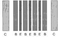
如图1所示,现有的SiGe HBT多采用多指结构(multi-finger)以提高电流的驱动能力,其实现方法为以发射极与(或)集电极为中心,两边对称排布,其排布方式为C/BE/BE/BE/B/…C,B为相邻的两个管子的发射极共用,在多指结构的两端各保留一个集电极,集电极之间通过贯通于整个多指结构下的埋层连接,最终完成多指结构HBT的制作。如图2所示,为现有SiGe HBT多指结构的单体结构示意图,包括了集电区114、基区111、发射区110。集电区114为形成于N型高掺杂埋层102上的中低掺杂的N型外延层,通过衬底101上的N型高掺杂埋层102和有源区中的N型高掺杂集电极引出端(collector pick-up)104以及在层间膜105上的深阱接触106连接到金属电极107,N型高掺杂集电极引出端104是通过高剂量、大能量的离子注入形成,N型高掺杂集电极引出端104区域面积较大,因此集电极带来的电容(侧面)比较大。集电区114两侧由浅槽氧化层103进行隔离,由于埋层102面积较大,为了减小集电区和衬底间寄生电容,在器件之间还需在浅槽隔离底部加一个深槽115并填入多晶硅进行隔离。基区111为在位P型掺杂的SiGe外延层,所述基区111通过多晶硅层108接电极引出,所述多晶硅层108底下为氧化硅介质层113。发射区110由一N型重掺杂多晶硅构成,形成于所述基区111上,发射极110的侧壁生长有氧化硅侧壁112,发射区110和所述基区111的接触面大小由氧化硅介质层109形成的窗口决定,在发射区窗口打开时可选择中心集电区局部离子注入,调节SiGe异质结双极晶体管的击穿电压和特征频率。基于频率特性的考虑,当采用多指结构以提高电流的驱动能力时,集电极必须放在整个结构的最外面,如图1所示。As shown in Figure 1, the existing SiGe HBT mostly adopts a multi-finger structure (multi-finger) to improve the current driving ability. The arrangement is C/BE/BE/BE/B/...C, B is shared by the emitters of two adjacent tubes, and a collector is reserved at each end of the multi-finger structure, and the collectors are connected through the The buried layer connection under the entire multi-finger structure finally completes the fabrication of the multi-finger structure HBT. As shown in FIG. 2 , it is a schematic diagram of a single structure of an existing SiGe HBT multi-finger structure, including a
这种多指结构成熟可靠,普遍应用,但主要缺点是:整个多指器件范围内需要有大面积的埋层作为集电极的连接和引出,因此会导致较大的结电容,影响器件的速度。同时由于整个多指结构发射极多,集电极少,电流在埋层以及集电极非常集中,必须把集电结做得很大以防止电流密度过大,因此进一步增大了电容。同理多指结构三极管往往只有两端有两个集电极而不会引入多个集电极以避免增大结面积影响速度。This kind of multi-finger structure is mature and reliable, and is widely used, but the main disadvantage is that a large area of buried layer is required in the whole range of multi-finger devices as the connection and lead-out of the collector, which will lead to large junction capacitance and affect the speed of the device. . At the same time, because the entire multi-finger structure has many emitters and few collectors, the current is very concentrated in the buried layer and the collector, so the collector junction must be made very large to prevent the current density from being too large, thus further increasing the capacitance. In the same way, multi-finger structure triodes often only have two collectors at both ends and will not introduce multiple collectors to avoid increasing the junction area and affecting the speed.
发明内容Contents of the invention
本发明所要解决的技术问题是提供一种SiGe异质结双极晶体管多指结构,能减少电容、降低集电极输出电阻、改善频率特性。The technical problem to be solved by the invention is to provide a multi-finger structure of a SiGe heterojunction bipolar transistor, which can reduce capacitance, reduce collector output resistance, and improve frequency characteristics.
为解决上述技术问题,本发明提供的SiGe异质结双极晶体管多指结构,由多个SiGe异质结双极晶体管单体组成,用SiGe异质结双极晶体管的发射极E、基极B、集电极C表示所述多指结构为C/BEBC/BEBC/BEBC/…/C,其中CBEBC表示一个SiGe异质结双极晶体管单体,C为相邻的两个SiGe异质结双极晶体管单体共用。SiGe异质结双极晶体管单体的有源区由浅槽场氧隔离,包括:一集电区,由形成于有源区中的N型杂质离子注入层构成,底部连接由两个N型赝埋层连接而形成的埋层,所述两个赝埋层通过在有源区两侧的浅槽底部注入N型杂质离子形成;通过在所述两个赝埋层上的场氧中制作深槽接触引出两个集电极;一基区,由形成于所述集电区上的P型SiGe外延层构成,通过两侧与其相连一多晶硅上制作金属接触引出两个基极;一发射区,由形成于所述基区上的N型多晶硅构成,直接在所述发射区上做金属接触引出一个发射极。In order to solve the above-mentioned technical problems, the SiGe heterojunction bipolar transistor multi-finger structure provided by the present invention is composed of a plurality of SiGe heterojunction bipolar transistor monomers, and the emitter E and the base of the SiGe heterojunction bipolar transistor B. Collector C indicates that the multi-finger structure is C/BEBC/BEBC/BEBC/.../C, where CBEBC indicates a single SiGe heterojunction bipolar transistor, and C is two adjacent SiGe heterojunction bipolar transistors. Pole transistor monomer shared. The active area of the SiGe heterojunction bipolar transistor is isolated by shallow trench field oxygen, including: a collector area, which is composed of an N-type impurity ion implantation layer formed in the active area, and the bottom connection is formed by two N-type pseudo The buried layer formed by connecting the buried layer, the two pseudo-buried layers are formed by implanting N-type impurity ions at the bottom of the shallow groove on both sides of the active region; Two collector electrodes are drawn out by groove contact; a base area is composed of a P-type SiGe epitaxial layer formed on the collector area, and two bases are drawn out by making metal contacts on polysilicon connected to it on both sides; an emitter area, It is composed of N-type polysilicon formed on the base region, and a metal contact is directly made on the emitter region to lead out an emitter.
所述两个赝埋层的注入杂质为磷、剂量为1e14~1e16cm-2、能量为2~50KeV。所述两个赝埋层注入时,有源区顶部用硬掩模层、其侧部用侧墙做掩模保护有源区,防止所述两个赝埋层的杂质注入到有源区。所述硬掩模层由第一层氧化膜-第二层氮化膜-第三层氧化膜构成,总的厚度由膺埋层离子注入能量决定,以注入不穿透硬掩模层为准,第一层氧化膜、第二层氮化膜、第三层氧化膜的厚度范围分别为


所述集电区的N型杂质离子注入的杂质为磷,注入剂量为5e12~1e14cm-2,在去除所述硬掩模层的第三层氧化膜后在全部的SiGe异质结双极晶体管区域进行注入。所述集电区的深槽接触是在深槽中填入钛-氮化钛过渡金属层以及金属钨形成。由所述赝埋层和金属接触直接形成集电极的欧姆接触,也能在所述集电区的深槽刻蚀后在所述深槽底部自对准注入N型杂质,实现集电极的欧姆接触。金属层淀积采用PVD或CVD方式,钛、氮化钛的厚度范围分别为
在定义所述基区窗口时采用两种刻蚀速率相差很大的材料,为了保护集电区和基区间的界面,第一层薄膜为氧化硅,第二层薄膜为多晶硅或者氮化硅。第一层薄膜厚度

本发明具有如下的有益效果:由于重参杂的埋层只在沟槽隔离处注入,因此结的整体电容会小很多。同时多指结构的重复性结构由C/BE/BE/BE/BE/…C改为C/BEBC/BEBC/BEBC/…C,在整个多指结构中多次出现集电极,平均每个发射极可以配备一个集电极,因此单个集电极和埋层的电流密度大大减小,同时电流通过集电极引出需要走过的路径从原来的跨越整个多指结构到优化后的不超过一个重复单元距离,因此电阻也大大减小,对改善频率特性有较大的帮助,而且并不增加整个的多指结构的面积。The invention has the following beneficial effects: since the heavily doped buried layer is implanted only at the trench isolation, the overall capacitance of the junction will be much smaller. At the same time, the repetitive structure of the multi-finger structure is changed from C/BE/BE/BE/BE/…C to C/BEBC/BEBC/BEBC/…C. The collector appears multiple times in the entire multi-finger structure, and the average The electrode can be equipped with a collector, so the current density of a single collector and the buried layer is greatly reduced, and at the same time, the path that the current needs to travel through the collector is from the original spanning the entire multi-finger structure to the optimized distance of no more than one repeating unit , so the resistance is also greatly reduced, which is of great help to improve the frequency characteristics, and does not increase the area of the entire multi-finger structure.
附图说明Description of drawings
下面结合附图和具体实施方式对本发明作进一步详细的说明:Below in conjunction with accompanying drawing and specific embodiment the present invention will be described in further detail:
图1是现有SiGe HBT多指结构示意图;Figure 1 is a schematic diagram of the existing SiGe HBT multi-finger structure;
图2是现有SiGe HBT多指结构的单体结构示意图;Figure 2 is a schematic diagram of a single structure of an existing SiGe HBT multi-finger structure;
图3是本发明SiGe异质结双极晶体管多指结构示意图;Fig. 3 is a schematic diagram of the multi-finger structure of the SiGe heterojunction bipolar transistor of the present invention;
图4是本发明SiGe异质结双极晶体管多指结构的单体结构示意图。Fig. 4 is a schematic diagram of a single structure of a multi-finger structure of a SiGe heterojunction bipolar transistor according to the present invention.
具体实施方式Detailed ways
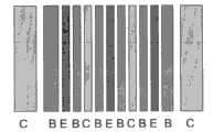
如图3所示,为本发明SiGe异质结双极晶体管多指结构示意图,由多个SiGe异质结双极晶体管单体组成,用SiGe异质结双极晶体管的发射极E、基极B、集电极C表示所述多指结构为C/BEBC/BEBC/BEBC/…/C,其中CBEBC表示一个SiGe异质结双极晶体管单体,C为相邻的两个SiGe异质结双极晶体管单体共用。As shown in Figure 3, it is a multi-finger structural schematic diagram of a SiGe heterojunction bipolar transistor of the present invention, which is composed of a plurality of SiGe heterojunction bipolar transistor monomers, with the emitter E and the base of the SiGe heterojunction bipolar transistor B. Collector C indicates that the multi-finger structure is C/BEBC/BEBC/BEBC/.../C, where CBEBC indicates a single SiGe heterojunction bipolar transistor, and C is two adjacent SiGe heterojunction bipolar transistors. Pole transistor monomer shared.
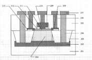
如图4所示,为本发明SiGe异质结双极晶体管多指结构的单体结构示意图。SiGe异质结双极晶体管单体的有源区由浅槽场氧隔离,包括:一集电区214,由形成于有源区中的N型杂质离子注入层构成,底部连接由两个N型赝埋层202连接而形成的埋层,所述两个赝埋层202通过在有源区两侧的浅槽底部注入N型杂质离子形成;通过在所述两个赝埋层上的场氧203中制作深槽接触204引出两个集电极,最后和金属层207相连;一基区211,由形成于所述集电区214上的P型SiGe外延层构成,通过两侧与所述基区相连一多晶硅208上制作金属接触引出两个基极;一发射区210,由形成于所述基区上的N型多晶硅构成,直接在所述发射区上做金属接触206引出一个发射极。As shown in FIG. 4 , it is a schematic diagram of a single structure of a multi-finger structure of a SiGe heterojunction bipolar transistor of the present invention. The active region of the SiGe heterojunction bipolar transistor monomer is isolated by shallow trench field oxygen, including: a
所述两个赝埋层202的注入杂质为磷、剂量为1e14~1e16cm-2、能量为2~50KeV。所述两个赝埋层202注入时,有源区顶部用硬掩模层、其侧部用侧墙做掩模保护有源区,防止所述两个赝埋层202的杂质注入到有源区。所述硬掩模层由第一层氧化膜-第二层氮化膜-第三层氧化膜构成,总的厚度由膺埋层离子注入能量决定,以注入不穿透硬掩模层为准,第一层氧化膜、第二层氮化膜、第三层氧化膜的厚度范围分别为


所述集电区214的N型杂质离子注入的杂质为磷,注入剂量为5e12~1e14cm-2,在去除所述硬掩模层的第三层氧化膜后在全部的SiGe异质结双极晶体管区域进行注入。所述集电区214的深槽接触204是在深槽中填入钛-氮化钛过渡金属层以及金属钨形成。由所述赝埋层202和金属接触直接形成集电极的欧姆接触,也能在所述集电区214的深槽刻蚀后在所述深槽底部自对准注入N型杂质,实现集电极的欧姆接触。金属层淀积采用PVD或CVD方式,钛、氮化钛的厚度范围分别为

在定义所述基区窗口时采用两种刻蚀速率相差很大的材料,为了保护集电区和基区间的界面,第一层薄膜213为氧化硅,第二层薄膜208为多晶硅或者氮化硅。第一层薄膜厚度第二层薄膜厚度

本发明的深槽接触204相比现有的有源区扩散性集电极104,节约了很多的面积。同时由于集电极的引入在浅槽场氧内,不会有较大的集电极电容,因此为了提高电流驱动能力采用多指结构时,可以增加集电极的数目,一方面降低了电流通路的距离,另一方面减小了集电极电流密度,帮助减小面积。Compared with the existing diffuse
以上通过具体实施例对本发明进行了详细的说明,但这些并非构成对本发明的限制。在不脱离本发明原理的情况下,本领域的技术人员还可做出许多变形和改进,这些也应视为本发明的保护范围。The present invention has been described in detail through specific examples above, but these do not constitute a limitation to the present invention. Without departing from the principle of the present invention, those skilled in the art can also make many modifications and improvements, which should also be regarded as the protection scope of the present invention.
Claims (14)
Translated fromChinese


Priority Applications (2)
| Application Number | Priority Date | Filing Date | Title |
|---|---|---|---|
| CN200910202009.XACN102231379B (en) | 2009-12-21 | 2009-12-21 | SiGe HBT (Heterojunction Bipolar Transistor) multi-finger structure |
| US12/971,063US8227832B2 (en) | 2009-12-21 | 2010-12-17 | SiGe heterojunction bipolar transistor multi-finger structure |
Applications Claiming Priority (1)
| Application Number | Priority Date | Filing Date | Title |
|---|---|---|---|
| CN200910202009.XACN102231379B (en) | 2009-12-21 | 2009-12-21 | SiGe HBT (Heterojunction Bipolar Transistor) multi-finger structure |
Publications (2)
| Publication Number | Publication Date |
|---|---|
| CN102231379A CN102231379A (en) | 2011-11-02 |
| CN102231379Btrue CN102231379B (en) | 2013-03-13 |
Family
ID=44149834
Family Applications (1)
| Application Number | Title | Priority Date | Filing Date |
|---|---|---|---|
| CN200910202009.XAActiveCN102231379B (en) | 2009-12-21 | 2009-12-21 | SiGe HBT (Heterojunction Bipolar Transistor) multi-finger structure |
Country Status (2)
| Country | Link |
|---|---|
| US (1) | US8227832B2 (en) |
| CN (1) | CN102231379B (en) |
Families Citing this family (20)
| Publication number | Priority date | Publication date | Assignee | Title |
|---|---|---|---|---|
| CN102117749B (en)* | 2009-12-31 | 2012-07-11 | 上海华虹Nec电子有限公司 | Manufacturing process of collector region and collector region buried layer of bipolar transistor |
| CN102117748B (en)* | 2009-12-31 | 2012-06-20 | 上海华虹Nec电子有限公司 | Method for manufacturing collector region and collector region buried layer of bipolar transistor |
| CN102403344B (en)* | 2010-09-10 | 2013-09-11 | 上海华虹Nec电子有限公司 | Parasitic PNP bipolar transistor in silicon germanium BiCMOS (bipolar complementary metal oxide semiconductor) process |
| CN102446965B (en)* | 2010-10-14 | 2013-09-11 | 上海华虹Nec电子有限公司 | Germanium-silicon heterojunction bipolar transistor |
| CN103107185B (en)* | 2011-11-11 | 2015-04-08 | 上海华虹宏力半导体制造有限公司 | Germanium-silicon power heterojunction bipolar transistor (HBT), manufacturing method thereof and germanium-silicon power HBT multi-pointing device |
| CN103137676B (en)* | 2011-11-23 | 2016-04-13 | 上海华虹宏力半导体制造有限公司 | A kind of Ge-Si heterojunction bipolar transistor and manufacture method thereof |
| US8648388B2 (en) | 2012-02-15 | 2014-02-11 | International Business Machines Corporation | High performance multi-finger strained silicon germanium channel PFET and method of fabrication |
| CN103050521B (en)* | 2012-05-23 | 2015-02-04 | 上海华虹宏力半导体制造有限公司 | Collector region lead-out structure for SiGe heterojunction bipolar transistor (HBT) device, and manufacturing method for collector region lead-out structure |
| CN103035690B (en)* | 2012-06-08 | 2015-06-03 | 上海华虹宏力半导体制造有限公司 | Ultrahigh pressure germanium-silicon hetero-junction bipolar transistor and manufacturing method thereof |
| RU2507633C1 (en)* | 2012-09-24 | 2014-02-20 | Федеральное Государственное Унитарное Предприятие "Научно-Производственное Предприятие "Пульсар" | Bipolar transistor based on heteroepitaxial structures and method of its realisation |
| CN103050522A (en)* | 2012-12-06 | 2013-04-17 | 上海华虹Nec电子有限公司 | Lateral parasitic PNP triode in SiGe heterojunction bipolar transistor (HBT) process and manufacturing method for lateral parasitic PNP triode |
| US9006833B2 (en)* | 2013-07-02 | 2015-04-14 | Texas Instruments Incorporated | Bipolar transistor having sinker diffusion under a trench |
| US10553633B2 (en)* | 2014-05-30 | 2020-02-04 | Klaus Y.J. Hsu | Phototransistor with body-strapped base |
| US9543403B2 (en)* | 2015-01-21 | 2017-01-10 | Globalfoundries Inc. | Bipolar junction transistor with multiple emitter fingers |
| US10431654B2 (en)* | 2015-06-25 | 2019-10-01 | International Business Machines Corporation | Extrinsic base doping for bipolar junction transistors |
| US9812447B2 (en) | 2016-02-02 | 2017-11-07 | Globalfoundries Inc. | Bipolar junction transistors with extrinsic device regions free of trench isolation |
| CN107728190B (en)* | 2017-09-30 | 2023-09-26 | 天津大学 | Radiation intensity detector based on multi-finger SiGe HBT |
| CN111081702B (en)* | 2019-11-18 | 2022-05-31 | 北京工业大学 | A SiGeHBT Array with Isothermal Distribution of Dielectric Trench Isolation Structure |
| US11721719B2 (en)* | 2020-10-20 | 2023-08-08 | Globalfoundries U.S. Inc. | Heterojunction bipolar transistor with buried trap rich isolation region |
| US12336206B2 (en)* | 2022-11-21 | 2025-06-17 | Globalfoundries U.S. Inc. | Heterojunction bipolar transistors with a cut stress liner |
Citations (1)
| Publication number | Priority date | Publication date | Assignee | Title |
|---|---|---|---|---|
| CN1294414A (en)* | 1999-10-21 | 2001-05-09 | 松下电器产业株式会社 | Horizontal heterojunction dual-polar triode and its mfg. method |
Family Cites Families (2)
| Publication number | Priority date | Publication date | Assignee | Title |
|---|---|---|---|---|
| JPH0897230A (en)* | 1994-09-22 | 1996-04-12 | Nec Corp | Bipolar transistor |
| US6972463B2 (en)* | 2003-10-20 | 2005-12-06 | United Microelectronics Corp. | Multi-finger transistor |
- 2009
- 2009-12-21CNCN200910202009.XApatent/CN102231379B/enactiveActive
- 2010
- 2010-12-17USUS12/971,063patent/US8227832B2/enactiveActive
Patent Citations (1)
| Publication number | Priority date | Publication date | Assignee | Title |
|---|---|---|---|---|
| CN1294414A (en)* | 1999-10-21 | 2001-05-09 | 松下电器产业株式会社 | Horizontal heterojunction dual-polar triode and its mfg. method |
Non-Patent Citations (1)
| Title |
|---|
| JP特开平8-97230A 1996.04.12 |
Also Published As
| Publication number | Publication date |
|---|---|
| CN102231379A (en) | 2011-11-02 |
| US8227832B2 (en) | 2012-07-24 |
| US20110147793A1 (en) | 2011-06-23 |
Similar Documents
| Publication | Publication Date | Title |
|---|---|---|
| CN102231379B (en) | SiGe HBT (Heterojunction Bipolar Transistor) multi-finger structure | |
| CN102104062B (en) | bipolar transistor | |
| CN102097464B (en) | High-voltage bipolar transistor | |
| CN102446965B (en) | Germanium-silicon heterojunction bipolar transistor | |
| CN102437180B (en) | Ultra high voltage silicon germanium heterojunction bipolar transistor (HBT) device and manufacturing method thereof | |
| TW200308032A (en) | A method and structure for low capacitance ESD robust diodes | |
| CN102044560B (en) | Ultrahigh frequency silicon and germanium heterojunction bipolar transistor | |
| CN113838916A (en) | Separation gate CSTBT with PMOS current clamping and manufacturing method thereof | |
| CN113838914A (en) | RET IGBT device structure and fabrication method with split gate structure | |
| CN114899239A (en) | Silicon carbide MOSFET and preparation method thereof | |
| CN114464676A (en) | Reverse conducting IGBT | |
| CN103035689B (en) | Collector region out-leading structure of germanium-silicon heterojunction bipolar transistor (HBT) and manufacturing method thereof | |
| CN103066101B (en) | Germanium silicium HBT device and manufacture method | |
| CN110473905B (en) | A split gate TIGBT with self-biased PMOS and method of making the same | |
| CN103117300B (en) | Parasitic lateral type PNP device and manufacture method | |
| US8759880B2 (en) | Ultra-high voltage SIGE HBT device and manufacturing method of the same | |
| US8455975B2 (en) | Parasitic PNP bipolar transistor in a silicon-germanium BiCMOS process | |
| US8866189B2 (en) | Silicon-germanium heterojunction bipolar transistor and manufacturing method thereof | |
| CN102468329B (en) | Silicon germanium heterojunction bipolar transistor multi-fingered structure | |
| CN103137673B (en) | Self-alignment bipolar transistor and manufacturing method thereof | |
| CN102104065B (en) | Parasitic lateral PNP triode in SiGe heterojunction bipolar transistor process | |
| CN214203693U (en) | Power semiconductor, transistor and electronic device | |
| CN102412275A (en) | Vertical PNP device in SiGe BiCMOS technology and manufacturing method thereof | |
| CN103066117B (en) | Half self alignment bipolar transistor and manufacturing method thereof | |
| CN103066119B (en) | Germanium silicon heterojunction bipolar transistor and manufacturing method thereof |
Legal Events
| Date | Code | Title | Description |
|---|---|---|---|
| C06 | Publication | ||
| PB01 | Publication | ||
| C10 | Entry into substantive examination | ||
| SE01 | Entry into force of request for substantive examination | ||
| C14 | Grant of patent or utility model | ||
| GR01 | Patent grant | ||
| ASS | Succession or assignment of patent right | Owner name:SHANGHAI HUAHONG GRACE SEMICONDUCTOR MANUFACTURING Free format text:FORMER OWNER: HUAHONG NEC ELECTRONICS CO LTD, SHANGHAI Effective date:20131216 | |
| C41 | Transfer of patent application or patent right or utility model | ||
| COR | Change of bibliographic data | Free format text:CORRECT: ADDRESS; FROM: 201206 PUDONG NEW AREA, SHANGHAI TO: 201203 PUDONG NEW AREA, SHANGHAI | |
| TR01 | Transfer of patent right | Effective date of registration:20131216 Address after:201203 Shanghai city Zuchongzhi road Pudong New Area Zhangjiang hi tech Park No. 1399 Patentee after:Shanghai Huahong Grace Semiconductor Manufacturing Corporation Address before:201206, Shanghai, Pudong New Area, Sichuan Road, No. 1188 Bridge Patentee before:Shanghai Huahong NEC Electronics Co., Ltd. |