CN102217179A - Dc-dc converter - Google Patents
Dc-dc converterDownload PDFInfo
- Publication number
- CN102217179A CN102217179ACN2010800032337ACN201080003233ACN102217179ACN 102217179 ACN102217179 ACN 102217179ACN 2010800032337 ACN2010800032337 ACN 2010800032337ACN 201080003233 ACN201080003233 ACN 201080003233ACN 102217179 ACN102217179 ACN 102217179A
- Authority
- CN
- China
- Prior art keywords
- switch
- output
- control
- circuit
- lower edge
- Prior art date
- Legal status (The legal status is an assumption and is not a legal conclusion. Google has not performed a legal analysis and makes no representation as to the accuracy of the status listed.)
- Granted
Links
Images


Classifications
- H—ELECTRICITY
- H02—GENERATION; CONVERSION OR DISTRIBUTION OF ELECTRIC POWER
- H02M—APPARATUS FOR CONVERSION BETWEEN AC AND AC, BETWEEN AC AND DC, OR BETWEEN DC AND DC, AND FOR USE WITH MAINS OR SIMILAR POWER SUPPLY SYSTEMS; CONVERSION OF DC OR AC INPUT POWER INTO SURGE OUTPUT POWER; CONTROL OR REGULATION THEREOF
- H02M3/00—Conversion of DC power input into DC power output
- H02M3/02—Conversion of DC power input into DC power output without intermediate conversion into AC
- H02M3/04—Conversion of DC power input into DC power output without intermediate conversion into AC by static converters
- H02M3/10—Conversion of DC power input into DC power output without intermediate conversion into AC by static converters using discharge tubes with control electrode or semiconductor devices with control electrode
- H02M3/145—Conversion of DC power input into DC power output without intermediate conversion into AC by static converters using discharge tubes with control electrode or semiconductor devices with control electrode using devices of a triode or transistor type requiring continuous application of a control signal
- H02M3/155—Conversion of DC power input into DC power output without intermediate conversion into AC by static converters using discharge tubes with control electrode or semiconductor devices with control electrode using devices of a triode or transistor type requiring continuous application of a control signal using semiconductor devices only
- H02M3/156—Conversion of DC power input into DC power output without intermediate conversion into AC by static converters using discharge tubes with control electrode or semiconductor devices with control electrode using devices of a triode or transistor type requiring continuous application of a control signal using semiconductor devices only with automatic control of output voltage or current, e.g. switching regulators
- H02M3/158—Conversion of DC power input into DC power output without intermediate conversion into AC by static converters using discharge tubes with control electrode or semiconductor devices with control electrode using devices of a triode or transistor type requiring continuous application of a control signal using semiconductor devices only with automatic control of output voltage or current, e.g. switching regulators including plural semiconductor devices as final control devices for a single load
- H02M3/1588—Conversion of DC power input into DC power output without intermediate conversion into AC by static converters using discharge tubes with control electrode or semiconductor devices with control electrode using devices of a triode or transistor type requiring continuous application of a control signal using semiconductor devices only with automatic control of output voltage or current, e.g. switching regulators including plural semiconductor devices as final control devices for a single load comprising at least one synchronous rectifier element
- Y—GENERAL TAGGING OF NEW TECHNOLOGICAL DEVELOPMENTS; GENERAL TAGGING OF CROSS-SECTIONAL TECHNOLOGIES SPANNING OVER SEVERAL SECTIONS OF THE IPC; TECHNICAL SUBJECTS COVERED BY FORMER USPC CROSS-REFERENCE ART COLLECTIONS [XRACs] AND DIGESTS
- Y02—TECHNOLOGIES OR APPLICATIONS FOR MITIGATION OR ADAPTATION AGAINST CLIMATE CHANGE
- Y02B—CLIMATE CHANGE MITIGATION TECHNOLOGIES RELATED TO BUILDINGS, e.g. HOUSING, HOUSE APPLIANCES OR RELATED END-USER APPLICATIONS
- Y02B70/00—Technologies for an efficient end-user side electric power management and consumption
- Y02B70/10—Technologies improving the efficiency by using switched-mode power supplies [SMPS], i.e. efficient power electronics conversion e.g. power factor correction or reduction of losses in power supplies or efficient standby modes
Landscapes
- Engineering & Computer Science (AREA)
- Power Engineering (AREA)
- Dc-Dc Converters (AREA)
Abstract
Translated fromChineseDescription
Translated fromChinese技术领域technical field
本发明涉及DC-DC转换器,特别涉及DC-DC转换器中的高边开关的接通驱动电压的自举电路(bootstrap)。The present invention relates to DC-DC converters, and in particular to a bootstrap circuit (bootstrap) for turning on driving voltage of a high-side switch in a DC-DC converter.
背景技术Background technique
作为各种电子设备的直流电源,通常使用开关方式的DC-DC转换器。一般,DC-DC转换器对串联连接在输入电压与地之间的高边开关(high side switch)和低边开关(low side switch)进行开关控制,利用平滑电容器对蓄积在电感器中的电能进行平滑化来生成输出电压。As DC power supplies for various electronic devices, switching DC-DC converters are generally used. In general, a DC-DC converter performs switching control of a high side switch and a low side switch connected in series between an input voltage and ground, and uses a smoothing capacitor to smooth the electric energy stored in the inductor. Smoothing is performed to generate the output voltage.
有时为了DC-DC转换器的小型化和性能的提高,利用N沟道MOSFET来构成高边开关。此时,需要将高边开关的接通驱动电压设在输入电压以上,因此设置自举电路。自举电路具备连接在高边开关和低边开关之间的连接点上的电容器,以该电容器的充电电压提高高边开关的接通驱动电压。Sometimes in order to miniaturize and improve the performance of DC-DC converters, N-channel MOSFETs are used to form high-side switches. In this case, it is necessary to set the on-drive voltage of the high-side switch to be higher than the input voltage, so a bootstrap circuit is provided. The bootstrap circuit includes a capacitor connected to a connection point between the high-side switch and the low-side switch, and the on-drive voltage of the high-side switch is increased by the charged voltage of the capacitor.
一般,在高边开关的接通驱动电压的自举电路中,为了不使电容器的电荷逆流向电源侧,在电容器和电源之间设置二极管。此外,有时代替二极管而设置压降小的开关晶体管来阻止电容器的充电电压的降低(例如参照专利文献1)。In general, in a bootstrap circuit for turning on a drive voltage of a high-side switch, a diode is provided between the capacitor and the power supply so that the charges in the capacitor do not flow back to the power supply side. In addition, instead of a diode, a switching transistor with a small voltage drop may be provided to prevent a decrease in the charging voltage of the capacitor (for example, refer to Patent Document 1).
专利文献1:日本特开2007-195361号公报Patent Document 1: Japanese Patent Laid-Open No. 2007-195361
若自举电路想要将高边开关的接通驱动电压提高至输入电压以上,则必须使低边开关在一定程度的期间内维持接通状态,从而使电容器充分充电。但是,如待机时或过电压检测后的暂时停止时等那样,在DC-DC转换器的开关动作暂停的期间达到长时间的情况下,电容器会进行放电,高边开关的接通驱动电压无法充分被提高。其结果,即使在动作再次开始时对高边开关进行接通控制,高边开关也不会被接通,存在无法顺畅地再次启动DC-DC转换器的隐患。If the bootstrap circuit wants to increase the on-drive voltage of the high-side switch above the input voltage, it must keep the low-side switch on for a certain period of time to fully charge the capacitor. However, if the switching operation of the DC-DC converter is suspended for a long period of time, such as during standby or a temporary stop after overvoltage detection, the capacitor will be discharged, and the ON drive voltage of the high-side switch will be reduced. Fully raised. As a result, even if the high-side switch is controlled to be turned on when the operation is resumed, the high-side switch will not be turned on, and there is a possibility that the DC-DC converter cannot be restarted smoothly.
发明内容Contents of the invention
鉴于上述问题,本发明的课题是能够使具有自举电路的DC-DC转换器从长时间的开关暂停状态顺畅地恢复到通常状态。In view of the above problems, an object of the present invention is to smoothly restore a DC-DC converter having a bootstrap circuit from a long-time switching pause state to a normal state.
为了解决上述课题,本发明采用了如下的结构。即,一种对串联连接在输入电压与地之间的高边开关和低边开关分别进行开关控制,使输入电压降压来生成输出电压的DC-DC转换器,具备自举电路,该自举电路具有在低边开关处于接通状态时被充电的电容器,以电容器的充电电压来提高高边开关的接通驱动电压,在从对高边开关和低边开关的开关控制的暂停进行指示的暂停信号变成无效起的固定时间内,对高边开关进行关断控制,并且对低边开关进行接通控制,在经过固定时间之后,开始高边开关的接通控制。具体而言,DC-DC转换器除了上述自举电路外,还具备:控制电路,其对高边开关和低边开关进行开关控制;和固定时间触发电路,其在对高边开关和低边开关的开关控制的暂停进行指示的暂停信号变成无效时,使输出在固定时间内有效。并且,控制电路在固定时间触发电路的输出有效时,对高边开关进行关断控制,并且对低边开关进行接通控制。In order to solve the above-mentioned problems, the present invention employs the following configurations. That is, a DC-DC converter that performs on-off control of a high-side switch and a low-side switch that are connected in series between an input voltage and ground to generate an output voltage by stepping down an input voltage includes a bootstrap circuit. The lifting circuit has a capacitor that is charged when the low-side switch is in the on state, and the charge voltage of the capacitor is used to increase the turn-on drive voltage of the high-side switch, indicating that the switching control of the high-side switch and the low-side switch is suspended. The high-side switch is controlled to be off and the low-side switch is controlled to be on within a fixed time period from when the pause signal becomes invalid, and the high-side switch is turned on after the fixed time elapses. Specifically, the DC-DC converter has, in addition to the above-mentioned bootstrap circuit, a control circuit that performs switching control on the high-side switch and the low-side switch; and a fixed-time trigger circuit that performs switching control on the high-side switch and the low-side When the pause signal of the switch control pause instruction becomes invalid, the output is enabled for a fixed time. In addition, the control circuit controls the high side switch to be off and the low side switch to be on when the output of the trigger circuit for a fixed time is valid.
由此,在从暂停状态结束开始直到对高边开关进行接通控制为止的期间内,自举电路中的电容器被充电。因此,即使暂停状态持续很长时间而导致电容器放电,也能够在动作再次开始时使高边开关处于接通状态。由此、DC-DC转换器能够从暂停状态顺畅地恢复到通常状态。Thus, the capacitor in the bootstrap circuit is charged during the period from the end of the pause state until the ON control of the high-side switch is performed. Therefore, even if the capacitor is discharged due to the pause state continuing for a long time, the high side switch can be turned on when the operation is resumed. Accordingly, the DC-DC converter can smoothly return to the normal state from the suspended state.
(发明效果)(invention effect)
根据本发明,具有自举电路的DC-DC转换器能够从长时间的开关暂停状态顺畅地恢复到通常状态。According to the present invention, a DC-DC converter having a bootstrap circuit can smoothly return to a normal state from a long-time switching pause state.
附图说明Description of drawings
图1是第1实施方式的DC-DC转换器的结构图。FIG. 1 is a configuration diagram of a DC-DC converter according to a first embodiment.
图2是表示了图1中的固定时间触发电路的结构例的DC-DC转换器的结构图。FIG. 2 is a configuration diagram of a DC-DC converter showing a configuration example of a fixed-time flip-flop circuit in FIG. 1 .
图3是图1的DC-DC转换器的动作时序图。FIG. 3 is an operation timing chart of the DC-DC converter in FIG. 1 .
图4是第2实施方式的DC-DC转换器的结构图。FIG. 4 is a configuration diagram of a DC-DC converter according to a second embodiment.
图5是表示了图4中的固定时间触发电路的结构例的DC-DC转换器的结构图。FIG. 5 is a configuration diagram of a DC-DC converter showing a configuration example of the fixed-time flip-flop circuit in FIG. 4 .
图6是图4的DC-DC转换器的动作时序图。FIG. 6 is an operation timing chart of the DC-DC converter in FIG. 4 .
具体实施方式Detailed ways
(第1实施方式)(first embodiment)
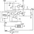
图1表示第1实施方式的DC-DC转换器的结构。在输入电压Vin和地之间串联连接有高边开关1和低边开关2。这些开关都由N沟道MOSFET构成,分别由驱动器11、12来驱动。并且,使这些开关以规定的时间比率交替地导通,利用平滑电容器4对蓄积在电感器3上的电能进行平滑化,从而生成输出电压Vout。FIG. 1 shows the configuration of a DC-DC converter according to the first embodiment. A high-side switch 1 and a low-
自举电路5可由电容器51和二极管52构成。在低边开关2为接通状态时,从控制用电压VDD经由二极管52对电容器51进行充电。电容器51的低电位端与高边开关1的源极和驱动器11的基准电位端连接。因此,高边开关1和低边开关2以规定的时间比率交替地导通,从而电容器51被充电至电压VDD程度,并将其电荷作为高边开关1的接通驱动电力来进行供给。另一方面,向驱动器12提供电压VDD,以电压VDD对低边开关2进行接通驱动。The
固定时间触发电路6在暂停信号BRK为无效(inactive)时,将作为输出的信号LON设为固定时间有效。暂停信号BRK是指示高边开关1和低边开关2的开关控制的暂停的信号,例如,若输出电压Vout达到允许上限值,则成为有效,若达到允许下限值,则成为无效。以下,为了便于说明,针对各信号,将有效设为“H”,将无效设为“L”。The fixed-
图2表示了固定时间触发电路6的结构例。固定时间触发电路6可由接收暂停信号BRK并将其延迟输出的延迟电路61、以及对暂停信号BRK的反相和延迟电路61的输出之间的逻辑与进行运算的逻辑电路62构成。延迟电路61可由通过电阻元件611和电容器612构成的CR电路来实现。此时,CR时间常数成为延迟时间。因此,通过变更电阻元件611和电容器612的至少一方的元件值,能够调整延迟时间。另外,代替延迟电路61,也可以设置刻画固定时间的定时电路。FIG. 2 shows a configuration example of the fixed-time flip-
回到图1,控制电路7经由驱动器11、12分别对高边开关1和低边开关2进行开关控制。具体而言,控制信号产生电路71在使能信号EN有效时工作,输出用于控制高边开关1的控制信号S1和用于控制低边开关2的控制信号S2。在暂停信号BRK无效且固定时间触发电路6的输出无效时,使能信号EN有效。具体而言,可作为对暂停信号BRK和信号LON的或非逻辑进行运算的逻辑电路72的输出,来赋予使能信号EN。将控制信号S1直接输入到驱动器11。另一方面,向驱动器12输入对控制信号S2和信号LON的逻辑或进行运算的逻辑电路73的输出。即,在控制信号S2有效或者固定时间触发电路6的输出有效时,对低边开关2进行接通控制。另外,在如图2所示那样构成固定时间触发电路6的情况下,也可以代替信号LON而向逻辑电路72输入延迟电路61的输出。Returning to FIG. 1 , the
图3表示本实施方式的DC-DC转换器的动作时序。在与DC-DC转换器连接的未图示的负载电路处于待机模式、即DC-DC转换器的负载非常轻的情况下,有时为了降低耗电,使DC-DC转换器间歇性工作。或者,若由于负载电流的急剧减少而在输出电压Vout中产生过冲,则有时需要暂时停止开关控制直到输出电压Vout恢复到目标值为止。在进行这样的间歇性动作时或过电压检测时等,暂停信号BRK在一定程度的期间内有效。若暂停信号BRK变成“H”,则使能信号EN变成“L”。因此,控制信号产生电路71停止工作,控制信号S1、S2都变成“L”。另一方面,在暂停信号BRK为“H”的期间,信号LON一直是“L”。FIG. 3 shows an operation sequence of the DC-DC converter of this embodiment. When an unillustrated load circuit connected to the DC-DC converter is in a standby mode, that is, when the load of the DC-DC converter is very light, the DC-DC converter may be operated intermittently in order to reduce power consumption. Alternatively, if an overshoot occurs in the output voltage Vout due to a sudden decrease in the load current, it may be necessary to temporarily stop the switching control until the output voltage Vout returns to the target value. During such intermittent operation or overvoltage detection, the pause signal BRK is valid for a certain period of time. When the pause signal BRK becomes "H", the enable signal EN becomes "L". Therefore, the operation of the control
若暂停期间结束而信号BRK变成“L”,则信号LON变成“H”,但使能信号EN在信号LON变成“H”的期间一直是“L”。因此,由于控制信号产生电路71不再次开始工作,因此高边开关1不会被接通控制。另一方面,通过信号LON变成“H”,对低边开关2进行接通控制。由此,高边开关1变成关断状态、低边开关2变成接通状态,在暂停期间内进行了放电的电容器51被充电。When the pause period ends and the signal BRK becomes "L", the signal LON becomes "H", but the enable signal EN is always "L" while the signal LON is "H". Therefore, since the control
若经过固定时间触发电路6刻画的固定时间而信号LON变成“L”,则使能信号EN变成“H”。由此,控制信号产生电路71再次开始工作。此时,由于电容器51被充分充电,因此DC-DC转换器能够顺畅地恢复到通常状态。When the signal LON becomes "L" after the fixed time defined by the fixed time flip-
以上,根据本实施方式,由于在暂停状态结束时对自举电路中的电容器进行充电,因此能够充分提高高边开关的接通驱动电压,从而能够顺畅地恢复到通常状态。As described above, according to the present embodiment, since the capacitor in the bootstrap circuit is charged at the end of the pause state, the on-drive voltage of the high-side switch can be sufficiently increased to smoothly return to the normal state.
(第2实施方式)(second embodiment)
图4表示第2实施方式的DC-DC转换器的结构。以下,说明与第1实施方式的不同点。FIG. 4 shows the configuration of a DC-DC converter according to the second embodiment. Differences from the first embodiment will be described below.
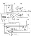
本实施方式的DC-DC转换器具备以迟滞幅度ΔV比较反馈了输出电压Vout的电压Vfb和基准电压Vr的迟滞比较器8。迟滞比较器8的输出成为暂停信号BRK。电压Vfb可以是输出电压Vout本身,也可以是将输出电压Vout电阻分压后的电压。The DC-DC converter of the present embodiment includes a
在控制电路7A中,作为暂停信号BRK的反相而提供控制信号产生电路71的使能信号EN。因此,若暂停状态结束,则控制信号产生电路71立即开始工作,再次启动未图示的外围电路,并且再次开始高边开关1和低边开关2的开关控制。暂停信号BRK成为无效之后的固定时间内,逻辑电路73的输出与控制信号S2无关地,根据固定时间触发电路6的输出而变成有效。因此,需要屏蔽控制信号S1,使得高边开关1和低边开关2不会同时成为接通状态。因此,向驱动器11输入对控制信号S1和信号LON的反相的逻辑与进行运算的逻辑电路74的输出。即,在控制信号S1有效且固定时间触发电路6的输出无效时,对高边开关1进行接通控制。In the
图5表示了固定时间触发电路6的结构例。延迟电路61A能够通过将反相电路连接多级来实现。通过变更其连接级数,能够调整延迟时间。另外,在如图5那样构成固定时间触发电路6的情况下,也可以代替信号LON而向逻辑电路74输入延迟电路61A的输出。FIG. 5 shows a configuration example of the fixed-time flip-
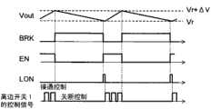
图6表示本实施方式的DC-DC转换器的动作时序。在如进行间歇性动作时这样的轻负载状态下,向电感器3提供比负载电流还大的电流,输出电压Vout上升。并且,若电压Vfb大于基准电压Vr+ΔV,则迟滞比较器8的输出即暂停信号BRK变成“H”。由此,使能信号EN变成“L”,控制信号产生电路71停止工作,高边开关1和低边开关2都处于关断状态,输出电压Vout下降。在这样的暂停期间内,通过使未图示的外围电路也停止工作,从而降低消耗电流。FIG. 6 shows an operation sequence of the DC-DC converter of this embodiment. In a light load state such as when intermittent operation is performed, a current larger than the load current is supplied to the
若输出电压Vout下降而导致电压Vfb小于基准电压Vr,则暂停信号BRK变成“L”。由此,使能信号EN变成“H”,控制信号产生电路71和未图示的外围电路开始工作。此外,由于信号LON变成“H”,因此对低边开关2进行接通控制。另一方面,由于屏蔽了控制信号S1,因此高边开关1一直是关断状态。由此,在暂停期间内放电的电容器51被充电。When the output voltage Vout falls so that the voltage Vfb is lower than the reference voltage Vr, the pause signal BRK becomes "L". Thereby, the enable signal EN becomes "H", and the control
若经过固定时间触发电路6刻画的固定时间而信号LON变成“L”,则控制信号S1的屏蔽被解除。由此,对高边开关1进行接通控制。此时,由于电容器51被充分充电,因此DC-DC转换器能够顺畅地恢复到通常状态。When the fixed time specified by the fixed
以上,根据本实施方式,能够在暂停状态结束时,在对自举电路的电容器进行充电的期间内再次开始外围电路的动作,因此能够更早恢复到通常状态。As described above, according to the present embodiment, when the suspend state ends, the operation of the peripheral circuit can be restarted while the capacitor of the bootstrap circuit is being charged, so that the normal state can be restored earlier.
另外,在上述各实施方式中,也可以代替自举电路5中的二极管52而使用开关晶体管来进行同步整流。此外,逻辑电路72、73、74可根据输入的信号逻辑而进行各种变形。In addition, in each of the above-described embodiments, a switching transistor may be used instead of the
此外,也可以在固定时间触发电路6的输出变成无效后,不立即进行高边开关1的接通控制。例如,也可以设置比固定时间触发电路6刻画更长时间的定时电路,在该定时电路的计时结束之后对高边开关1进行接通控制。此时,由于在暂停期间结束后立即对自举电路5中的电容器51进行充电,因此能够从暂停状态顺畅地恢复到通常状态。In addition, the ON control of the high-side switch 1 may not be performed immediately after the output of the fixed-time flip-
(产业上的可利用性)(industrial availability)
本发明的DC-DC转换器能够从暂停状态顺畅地恢复到通常状态,因此作为具有待机模式的负载电路的电源装置有用。Since the DC-DC converter of the present invention can smoothly return to a normal state from a pause state, it is useful as a power supply device having a load circuit in a standby mode.
符号说明Symbol Description
5 自举电路5 bootstrap circuit
51 电容器51 capacitor
6 固定时间触发电路6 Fixed time trigger circuit
61 延迟电路61 delay circuit
61A 延迟电路61A delay circuit
62 逻辑电路62 logic circuit
7 控制电路7 control circuit
72 逻辑电路(第一逻辑电路)72 logic circuit (first logic circuit)
73 逻辑电路(第二逻辑电路)73 logic circuit (second logic circuit)
74 逻辑电路(第一逻辑电路)74 logic circuit (first logic circuit)
71 控制信号产生电路71 Control signal generating circuit
8 迟滞比较器8 hysteresis comparators
Claims (6)
Applications Claiming Priority (3)
| Application Number | Priority Date | Filing Date | Title |
|---|---|---|---|
| JP2009252874AJP5330962B2 (en) | 2009-11-04 | 2009-11-04 | DC-DC converter |
| JP2009-252874 | 2009-11-04 | ||
| PCT/JP2010/004481WO2011055472A1 (en) | 2009-11-04 | 2010-07-09 | Dc-dc converter |
Publications (2)
| Publication Number | Publication Date |
|---|---|
| CN102217179Atrue CN102217179A (en) | 2011-10-12 |
| CN102217179B CN102217179B (en) | 2014-08-27 |
Family
ID=43969715
Family Applications (1)
| Application Number | Title | Priority Date | Filing Date |
|---|---|---|---|
| CN201080003233.7AExpired - Fee RelatedCN102217179B (en) | 2009-11-04 | 2010-07-09 | Dc-dc converter |
Country Status (4)
| Country | Link |
|---|---|
| US (1) | US8558526B2 (en) |
| JP (1) | JP5330962B2 (en) |
| CN (1) | CN102217179B (en) |
| WO (1) | WO2011055472A1 (en) |
Cited By (4)
| Publication number | Priority date | Publication date | Assignee | Title |
|---|---|---|---|---|
| TWI419452B (en)* | 2011-11-15 | 2013-12-11 | Lextar Electronics Corp | Bootstrap circuit and electronic device applying the same |
| CN110460226A (en)* | 2018-05-07 | 2019-11-15 | 欧姆龙株式会社 | Switching power unit |
| CN110932550A (en)* | 2019-12-26 | 2020-03-27 | 上海贝岭股份有限公司 | Voltage output circuit, switching power supply direct current converter and integrated circuit |
| CN111989851A (en)* | 2018-04-27 | 2020-11-24 | 华为技术有限公司 | A power circuit and device |
Families Citing this family (16)
| Publication number | Priority date | Publication date | Assignee | Title |
|---|---|---|---|---|
| TW201037953A (en)* | 2009-04-09 | 2010-10-16 | Anpec Electronics Corp | Direct current converter |
| TWI376869B (en)* | 2009-04-13 | 2012-11-11 | Anpec Electronics Corp | Direct current converter |
| ITMI20110388A1 (en)* | 2011-03-11 | 2012-09-12 | St Microelectronics Srl | DEVICE TO AVOID HARD-SWITCHING IN RESONATING CONVERTERS AND ITS METHOD. |
| CN102761245B (en)* | 2011-04-26 | 2016-06-29 | 国网新疆电力公司电力科学研究院 | Buck conversion circuit |
| JP6011761B2 (en) | 2011-12-19 | 2016-10-19 | パナソニックIpマネジメント株式会社 | Lighting device and lighting fixture using the same |
| TW201347381A (en)* | 2012-05-03 | 2013-11-16 | Anpec Electronics Corp | Direct current converter for bootstrap circuit |
| CN102832810B (en)* | 2012-08-30 | 2015-04-08 | 成都芯源系统有限公司 | Bootstrap voltage refresh control circuit, voltage conversion circuit and related control method |
| CN104838572A (en)* | 2012-12-03 | 2015-08-12 | 松下知识产权经营株式会社 | DC/DC convertor |
| US9431890B2 (en)* | 2013-02-20 | 2016-08-30 | Micron Technology, Inc. | Apparatuses and methods for converting single input voltage regulators to dual input voltage regulators |
| US9419509B2 (en)* | 2014-08-11 | 2016-08-16 | Texas Instruments Incorporated | Shared bootstrap capacitor for multiple phase buck converter circuit and methods |
| JP7266414B2 (en)* | 2019-01-28 | 2023-04-28 | リンナイ株式会社 | fan motor drive |
| JP7364316B2 (en)* | 2019-03-26 | 2023-10-18 | Fdk株式会社 | Power conversion device and power conversion control method |
| JP7327998B2 (en)* | 2019-05-17 | 2023-08-16 | ローム株式会社 | DC/DC converter |
| CN114448411B (en)* | 2020-11-02 | 2025-01-10 | 圣邦微电子(北京)股份有限公司 | Key control circuit, method and related equipment for battery connection or disconnection |
| US11942940B2 (en)* | 2021-02-05 | 2024-03-26 | Renesas Electronics America Inc. | Boot capacitor charge during low power states |
| KR20230027960A (en) | 2021-08-20 | 2023-02-28 | 삼성전자주식회사 | Buck convereter including bootstrap capacitor and operating method thereof |
Citations (4)
| Publication number | Priority date | Publication date | Assignee | Title |
|---|---|---|---|---|
| US20050030777A1 (en)* | 2003-08-08 | 2005-02-10 | Fujitsu Limited | DC/DC converter |
| JP2007028797A (en)* | 2005-07-15 | 2007-02-01 | Sanken Electric Co Ltd | Switching power supply unit |
| CN1926752A (en)* | 2004-12-08 | 2007-03-07 | 三垦电气株式会社 | Multi-output current-resonant type DC-DC converter |
| US20090146631A1 (en)* | 2005-07-11 | 2009-06-11 | Rohm Co., Ltd. | Step-down switching regulator |
Family Cites Families (9)
| Publication number | Priority date | Publication date | Assignee | Title |
|---|---|---|---|---|
| JP3233035B2 (en) | 1996-08-09 | 2001-11-26 | 株式会社村田製作所 | DC-DC converter |
| EP1087507B1 (en)* | 1999-09-21 | 2004-10-13 | STMicroelectronics S.r.l. | Method of controlling a DC-DC converter |
| IT1317125B1 (en)* | 2000-03-07 | 2003-05-27 | St Microelectronics Srl | CONSTANT FREQUENCY CONTROL CIRCUIT FOR A HYSTERETIC SWITCHING DENSITY REGULATOR |
| US6922044B2 (en)* | 2002-09-06 | 2005-07-26 | Intersil Americas Inc. | Synchronization of multiphase synthetic ripple voltage regulator |
| JP2004304527A (en) | 2003-03-31 | 2004-10-28 | Hitachi Ltd | Gate drive circuit and power supply control method thereof |
| JP4830507B2 (en) | 2006-01-20 | 2011-12-07 | 富士電機株式会社 | Bootstrap circuit |
| JP2007215259A (en)* | 2006-02-07 | 2007-08-23 | Matsushita Electric Ind Co Ltd | Driving circuit and switching regulator using the same |
| JP2010200554A (en)* | 2009-02-26 | 2010-09-09 | Fuji Electric Systems Co Ltd | Dc-dc converter |
| JP5586211B2 (en)* | 2009-11-17 | 2014-09-10 | 株式会社東芝 | DC-DC converter and semiconductor integrated circuit |
- 2009
- 2009-11-04JPJP2009252874Apatent/JP5330962B2/enactiveActive
- 2010
- 2010-07-09CNCN201080003233.7Apatent/CN102217179B/ennot_activeExpired - Fee Related
- 2010-07-09WOPCT/JP2010/004481patent/WO2011055472A1/enactiveApplication Filing
- 2011
- 2011-03-09USUS13/044,284patent/US8558526B2/enactiveActive
Patent Citations (4)
| Publication number | Priority date | Publication date | Assignee | Title |
|---|---|---|---|---|
| US20050030777A1 (en)* | 2003-08-08 | 2005-02-10 | Fujitsu Limited | DC/DC converter |
| CN1926752A (en)* | 2004-12-08 | 2007-03-07 | 三垦电气株式会社 | Multi-output current-resonant type DC-DC converter |
| US20090146631A1 (en)* | 2005-07-11 | 2009-06-11 | Rohm Co., Ltd. | Step-down switching regulator |
| JP2007028797A (en)* | 2005-07-15 | 2007-02-01 | Sanken Electric Co Ltd | Switching power supply unit |
Cited By (6)
| Publication number | Priority date | Publication date | Assignee | Title |
|---|---|---|---|---|
| TWI419452B (en)* | 2011-11-15 | 2013-12-11 | Lextar Electronics Corp | Bootstrap circuit and electronic device applying the same |
| CN111989851A (en)* | 2018-04-27 | 2020-11-24 | 华为技术有限公司 | A power circuit and device |
| US11201620B2 (en) | 2018-04-27 | 2021-12-14 | Huawei Technologies Co., Ltd. | Power supply circuit and apparatus |
| CN111989851B (en)* | 2018-04-27 | 2022-01-14 | 华为技术有限公司 | Power supply circuit and device |
| CN110460226A (en)* | 2018-05-07 | 2019-11-15 | 欧姆龙株式会社 | Switching power unit |
| CN110932550A (en)* | 2019-12-26 | 2020-03-27 | 上海贝岭股份有限公司 | Voltage output circuit, switching power supply direct current converter and integrated circuit |
Also Published As
| Publication number | Publication date |
|---|---|
| US8558526B2 (en) | 2013-10-15 |
| US20110156669A1 (en) | 2011-06-30 |
| JP5330962B2 (en) | 2013-10-30 |
| CN102217179B (en) | 2014-08-27 |
| JP2011101452A (en) | 2011-05-19 |
| WO2011055472A1 (en) | 2011-05-12 |
Similar Documents
| Publication | Publication Date | Title |
|---|---|---|
| CN102217179B (en) | Dc-dc converter | |
| JP5125066B2 (en) | Control circuit for synchronous rectification type DC-DC converter, synchronous rectification type DC-DC converter and control method therefor | |
| CN105391298B (en) | Dc-dc converter control | |
| US7830131B2 (en) | Control circuit for switching regulator | |
| CN101106326B (en) | Dc-dc converter | |
| JP4481879B2 (en) | Switching power supply | |
| JP4347249B2 (en) | DC-DC converter, control circuit for DC-DC converter, and control method for DC-DC converter | |
| JP4734382B2 (en) | Integrated circuit for DC-DC converter | |
| JP5910395B2 (en) | Drive circuit | |
| JP2004173460A (en) | Control method of DC-DC converter, DC-DC converter, semiconductor integrated circuit device, and electronic device | |
| WO2006120842A1 (en) | Switching regulator and electronic device having same | |
| JP2000197348A (en) | DC-DC converter circuit | |
| JP2010200554A (en) | Dc-dc converter | |
| US20100085776A1 (en) | Switching power supply apparatus | |
| JP2008079448A (en) | Boost power supply | |
| JP3699082B2 (en) | Switching power supply circuit | |
| JP2010213559A (en) | Dc power supply and dc-dc converter | |
| JP5825433B2 (en) | Switching power supply | |
| JP5304173B2 (en) | Power supply voltage control circuit and DC-DC converter | |
| CN103560669B (en) | Step-up/step-down type dc-dc converter and control circuit thereof and control method | |
| JP5428713B2 (en) | DC-DC converter and control method thereof | |
| JP2011200009A (en) | Switching power supply | |
| US8890498B2 (en) | Driving circuit to turn off switching element by voltage from voltage storage unit and converter including driving circuit | |
| JP3289680B2 (en) | Power supply inrush current prevention circuit | |
| JP6619662B2 (en) | Switching regulator |
Legal Events
| Date | Code | Title | Description |
|---|---|---|---|
| C06 | Publication | ||
| PB01 | Publication | ||
| C10 | Entry into substantive examination | ||
| SE01 | Entry into force of request for substantive examination | ||
| C14 | Grant of patent or utility model | ||
| GR01 | Patent grant | ||
| TR01 | Transfer of patent right | Effective date of registration:20200529 Address after:Kyoto Japan Patentee after:Panasonic semiconductor solutions Co.,Ltd. Address before:Osaka Japan Patentee before:Matsushita Electric Industrial Co.,Ltd. | |
| TR01 | Transfer of patent right | ||
| CF01 | Termination of patent right due to non-payment of annual fee | Granted publication date:20140827 | |
| CF01 | Termination of patent right due to non-payment of annual fee |