CN102214579B - Manufacturing method of semiconductor element and semiconductor element - Google Patents
Manufacturing method of semiconductor element and semiconductor elementDownload PDFInfo
- Publication number
- CN102214579B CN102214579BCN201010568174.XACN201010568174ACN102214579BCN 102214579 BCN102214579 BCN 102214579BCN 201010568174 ACN201010568174 ACN 201010568174ACN 102214579 BCN102214579 BCN 102214579B
- Authority
- CN
- China
- Prior art keywords
- gate
- layer
- forming
- metal layer
- polysilicon
- Prior art date
- Legal status (The legal status is an assumption and is not a legal conclusion. Google has not performed a legal analysis and makes no representation as to the accuracy of the status listed.)
- Expired - Fee Related
Links
- 239000004065semiconductorSubstances0.000titleclaimsabstractdescription59
- 238000004519manufacturing processMethods0.000titleclaimsabstractdescription17
- 239000010410layerSubstances0.000claimsabstractdescription236
- 229910021420polycrystalline siliconInorganic materials0.000claimsabstractdescription82
- 229920005591polysiliconPolymers0.000claimsabstractdescription82
- 229910052751metalInorganic materials0.000claimsabstractdescription77
- 239000002184metalSubstances0.000claimsabstractdescription77
- 239000000758substrateSubstances0.000claimsabstractdescription45
- 238000011049fillingMethods0.000claimsabstractdescription22
- 239000011229interlayerSubstances0.000claimsabstractdescription20
- 239000000126substanceSubstances0.000claimsabstractdescription13
- 238000005498polishingMethods0.000claimsabstractdescription11
- 239000011241protective layerSubstances0.000claimsabstractdescription10
- 238000000034methodMethods0.000claimsdescription132
- 229910052710siliconInorganic materials0.000claimsdescription18
- 239000010703siliconSubstances0.000claimsdescription18
- 239000000463materialSubstances0.000claimsdescription17
- 229910000577Silicon-germaniumInorganic materials0.000claimsdescription12
- 238000005530etchingMethods0.000claimsdescription12
- LEVVHYCKPQWKOP-UHFFFAOYSA-N[Si].[Ge]Chemical compound[Si].[Ge]LEVVHYCKPQWKOP-UHFFFAOYSA-N0.000claimsdescription9
- 229910044991metal oxideInorganic materials0.000claims2
- 150000004706metal oxidesChemical class0.000claims2
- 230000035945sensitivityEffects0.000abstractdescription3
- 230000006870functionEffects0.000description25
- 229920002120photoresistant polymerPolymers0.000description24
- XUIMIQQOPSSXEZ-UHFFFAOYSA-NSiliconChemical compound[Si]XUIMIQQOPSSXEZ-UHFFFAOYSA-N0.000description16
- 230000005669field effectEffects0.000description12
- 125000006850spacer groupChemical group0.000description12
- 238000001312dry etchingMethods0.000description8
- FVBUAEGBCNSCDD-UHFFFAOYSA-Nsilicide(4-)Chemical group[Si-4]FVBUAEGBCNSCDD-UHFFFAOYSA-N0.000description8
- 238000005229chemical vapour depositionMethods0.000description7
- 238000000206photolithographyMethods0.000description7
- 238000005240physical vapour depositionMethods0.000description7
- 229910052814silicon oxideInorganic materials0.000description7
- 238000001039wet etchingMethods0.000description7
- VYPSYNLAJGMNEJ-UHFFFAOYSA-NSilicium dioxideChemical compoundO=[Si]=OVYPSYNLAJGMNEJ-UHFFFAOYSA-N0.000description6
- 238000000151depositionMethods0.000description6
- 239000003989dielectric materialSubstances0.000description6
- HBMJWWWQQXIZIP-UHFFFAOYSA-Nsilicon carbideChemical compound[Si+]#[C-]HBMJWWWQQXIZIP-UHFFFAOYSA-N0.000description6
- 229910010271silicon carbideInorganic materials0.000description6
- 238000000231atomic layer depositionMethods0.000description5
- 238000000059patterningMethods0.000description5
- 229910052581Si3N4Inorganic materials0.000description4
- 229910052782aluminiumInorganic materials0.000description4
- 239000010949copperSubstances0.000description4
- 229910052732germaniumInorganic materials0.000description4
- GNPVGFCGXDBREM-UHFFFAOYSA-Ngermanium atomChemical compound[Ge]GNPVGFCGXDBREM-UHFFFAOYSA-N0.000description4
- 238000007789sealingMethods0.000description4
- 229910021332silicideInorganic materials0.000description4
- HQVNEWCFYHHQES-UHFFFAOYSA-Nsilicon nitrideChemical compoundN12[Si]34N5[Si]62N3[Si]51N64HQVNEWCFYHHQES-UHFFFAOYSA-N0.000description4
- ATJFFYVFTNAWJD-UHFFFAOYSA-NTinChemical compound[Sn]ATJFFYVFTNAWJD-UHFFFAOYSA-N0.000description3
- RTAQQCXQSZGOHL-UHFFFAOYSA-NTitaniumChemical compound[Ti]RTAQQCXQSZGOHL-UHFFFAOYSA-N0.000description3
- XAGFODPZIPBFFR-UHFFFAOYSA-NaluminiumChemical compound[Al]XAGFODPZIPBFFR-UHFFFAOYSA-N0.000description3
- 229910052802copperInorganic materials0.000description3
- 230000008021depositionEffects0.000description3
- 239000002019doping agentSubstances0.000description3
- 238000000226double patterning lithographyMethods0.000description3
- 238000005516engineering processMethods0.000description3
- 229910000449hafnium oxideInorganic materials0.000description3
- 238000002513implantationMethods0.000description3
- 238000002955isolationMethods0.000description3
- 229910052718tinInorganic materials0.000description3
- 239000010936titaniumSubstances0.000description3
- 229910052719titaniumInorganic materials0.000description3
- 229910052721tungstenInorganic materials0.000description3
- VHUUQVKOLVNVRT-UHFFFAOYSA-NAmmonium hydroxideChemical compound[NH4+].[OH-]VHUUQVKOLVNVRT-UHFFFAOYSA-N0.000description2
- JBRZTFJDHDCESZ-UHFFFAOYSA-NAsGaChemical compound[As]#[Ga]JBRZTFJDHDCESZ-UHFFFAOYSA-N0.000description2
- RYGMFSIKBFXOCR-UHFFFAOYSA-NCopperChemical compound[Cu]RYGMFSIKBFXOCR-UHFFFAOYSA-N0.000description2
- 229910001218Gallium arsenideInorganic materials0.000description2
- 229910000530Gallium indium arsenideInorganic materials0.000description2
- GPXJNWSHGFTCBW-UHFFFAOYSA-NIndium phosphideChemical compound[In]#PGPXJNWSHGFTCBW-UHFFFAOYSA-N0.000description2
- BLRPTPMANUNPDV-UHFFFAOYSA-NSilaneChemical compound[SiH4]BLRPTPMANUNPDV-UHFFFAOYSA-N0.000description2
- CEPICIBPGDWCRU-UHFFFAOYSA-N[Si].[Hf]Chemical compound[Si].[Hf]CEPICIBPGDWCRU-UHFFFAOYSA-N0.000description2
- 239000000908ammonium hydroxideSubstances0.000description2
- 238000000137annealingMethods0.000description2
- 239000006117anti-reflective coatingSubstances0.000description2
- QVGXLLKOCUKJST-UHFFFAOYSA-Natomic oxygenChemical compound[O]QVGXLLKOCUKJST-UHFFFAOYSA-N0.000description2
- 150000001875compoundsChemical class0.000description2
- 239000004020conductorSubstances0.000description2
- 239000008367deionised waterSubstances0.000description2
- 229910021641deionized waterInorganic materials0.000description2
- 238000005137deposition processMethods0.000description2
- 238000013461designMethods0.000description2
- 230000008014freezingEffects0.000description2
- 238000007710freezingMethods0.000description2
- ZQXQADNTSSMHJI-UHFFFAOYSA-Nhafnium(4+) oxygen(2-) tantalum(5+)Chemical compound[O-2].[Ta+5].[Hf+4]ZQXQADNTSSMHJI-UHFFFAOYSA-N0.000description2
- KQHQLIAOAVMAOW-UHFFFAOYSA-Nhafnium(4+) oxygen(2-) zirconium(4+)Chemical compound[O--].[O--].[O--].[O--].[Zr+4].[Hf+4]KQHQLIAOAVMAOW-UHFFFAOYSA-N0.000description2
- WIHZLLGSGQNAGK-UHFFFAOYSA-Nhafnium(4+);oxygen(2-)Chemical compound[O-2].[O-2].[Hf+4]WIHZLLGSGQNAGK-UHFFFAOYSA-N0.000description2
- KUVFGOLWQIXGBP-UHFFFAOYSA-Nhafnium(4+);oxygen(2-);titanium(4+)Chemical compound[O-2].[O-2].[O-2].[O-2].[Ti+4].[Hf+4]KUVFGOLWQIXGBP-UHFFFAOYSA-N0.000description2
- XLYOFNOQVPJJNP-UHFFFAOYSA-MhydroxideChemical compound[OH-]XLYOFNOQVPJJNP-UHFFFAOYSA-M0.000description2
- RPQDHPTXJYYUPQ-UHFFFAOYSA-Nindium arsenideChemical compound[In]#[As]RPQDHPTXJYYUPQ-UHFFFAOYSA-N0.000description2
- 239000012212insulatorSubstances0.000description2
- 239000007769metal materialSubstances0.000description2
- 230000003647oxidationEffects0.000description2
- 238000007254oxidation reactionMethods0.000description2
- 229910052760oxygenInorganic materials0.000description2
- 239000001301oxygenSubstances0.000description2
- 238000001020plasma etchingMethods0.000description2
- 238000000926separation methodMethods0.000description2
- 229910000077silaneInorganic materials0.000description2
- WFKWXMTUELFFGS-UHFFFAOYSA-NtungstenChemical compound[W]WFKWXMTUELFFGS-UHFFFAOYSA-N0.000description2
- 239000010937tungstenSubstances0.000description2
- XLYOFNOQVPJJNP-UHFFFAOYSA-NwaterChemical compoundOXLYOFNOQVPJJNP-UHFFFAOYSA-N0.000description2
- ZOXJGFHDIHLPTG-UHFFFAOYSA-NBoronChemical compound[B]ZOXJGFHDIHLPTG-UHFFFAOYSA-N0.000description1
- 229910019001CoSiInorganic materials0.000description1
- 229910005883NiSiInorganic materials0.000description1
- OAICVXFJPJFONN-UHFFFAOYSA-NPhosphorusChemical compound[P]OAICVXFJPJFONN-UHFFFAOYSA-N0.000description1
- 229910004166TaNInorganic materials0.000description1
- ILCYGSITMBHYNK-UHFFFAOYSA-N[Si]=O.[Hf]Chemical compound[Si]=O.[Hf]ILCYGSITMBHYNK-UHFFFAOYSA-N0.000description1
- 230000002411adverseEffects0.000description1
- MJGARAGQACZIPN-UHFFFAOYSA-Naluminum hafnium(4+) oxygen(2-)Chemical compound[O--].[O--].[Al+3].[Hf+4]MJGARAGQACZIPN-UHFFFAOYSA-N0.000description1
- 229910021417amorphous siliconInorganic materials0.000description1
- 238000013459approachMethods0.000description1
- 229910052785arsenicInorganic materials0.000description1
- RQNWIZPPADIBDY-UHFFFAOYSA-Narsenic atomChemical compound[As]RQNWIZPPADIBDY-UHFFFAOYSA-N0.000description1
- 230000015572biosynthetic processEffects0.000description1
- 229910052796boronInorganic materials0.000description1
- 238000005234chemical depositionMethods0.000description1
- 238000004140cleaningMethods0.000description1
- 239000011248coating agentSubstances0.000description1
- 238000000576coating methodMethods0.000description1
- 230000000295complement effectEffects0.000description1
- 230000007423decreaseEffects0.000description1
- 230000007547defectEffects0.000description1
- 238000011161developmentMethods0.000description1
- MROCJMGDEKINLD-UHFFFAOYSA-NdichlorosilaneChemical compoundCl[SiH2]ClMROCJMGDEKINLD-UHFFFAOYSA-N0.000description1
- 238000009792diffusion processMethods0.000description1
- 230000000694effectsEffects0.000description1
- 239000007789gasSubstances0.000description1
- PDKGWPFVRLGFBG-UHFFFAOYSA-Nhafnium(4+) oxygen(2-) silicon(4+)Chemical compound[O-2].[Hf+4].[Si+4].[O-2].[O-2].[O-2]PDKGWPFVRLGFBG-UHFFFAOYSA-N0.000description1
- 239000011810insulating materialSubstances0.000description1
- 238000009413insulationMethods0.000description1
- 238000005468ion implantationMethods0.000description1
- 230000000873masking effectEffects0.000description1
- -1metal compoundsChemical class0.000description1
- 150000002736metal compoundsChemical class0.000description1
- 150000002739metalsChemical class0.000description1
- 238000012986modificationMethods0.000description1
- 230000004048modificationEffects0.000description1
- 229910052750molybdenumInorganic materials0.000description1
- TWNQGVIAIRXVLR-UHFFFAOYSA-Noxo(oxoalumanyloxy)alumaneChemical compoundO=[Al]O[Al]=OTWNQGVIAIRXVLR-UHFFFAOYSA-N0.000description1
- RVTZCBVAJQQJTK-UHFFFAOYSA-Noxygen(2-);zirconium(4+)Chemical compound[O-2].[O-2].[Zr+4]RVTZCBVAJQQJTK-UHFFFAOYSA-N0.000description1
- 229910052698phosphorusInorganic materials0.000description1
- 239000011574phosphorusSubstances0.000description1
- 238000007517polishing processMethods0.000description1
- 238000009736wettingMethods0.000description1
- 229910001928zirconium oxideInorganic materials0.000description1
Images


Classifications
- H—ELECTRICITY
- H10—SEMICONDUCTOR DEVICES; ELECTRIC SOLID-STATE DEVICES NOT OTHERWISE PROVIDED FOR
- H10D—INORGANIC ELECTRIC SEMICONDUCTOR DEVICES
- H10D84/00—Integrated devices formed in or on semiconductor substrates that comprise only semiconducting layers, e.g. on Si wafers or on GaAs-on-Si wafers
- H10D84/80—Integrated devices formed in or on semiconductor substrates that comprise only semiconducting layers, e.g. on Si wafers or on GaAs-on-Si wafers characterised by the integration of at least one component covered by groups H10D12/00 or H10D30/00, e.g. integration of IGFETs
- H10D84/82—Integrated devices formed in or on semiconductor substrates that comprise only semiconducting layers, e.g. on Si wafers or on GaAs-on-Si wafers characterised by the integration of at least one component covered by groups H10D12/00 or H10D30/00, e.g. integration of IGFETs of only field-effect components
- H10D84/83—Integrated devices formed in or on semiconductor substrates that comprise only semiconducting layers, e.g. on Si wafers or on GaAs-on-Si wafers characterised by the integration of at least one component covered by groups H10D12/00 or H10D30/00, e.g. integration of IGFETs of only field-effect components of only insulated-gate FETs [IGFET]
- H10D84/85—Complementary IGFETs, e.g. CMOS
- H—ELECTRICITY
- H10—SEMICONDUCTOR DEVICES; ELECTRIC SOLID-STATE DEVICES NOT OTHERWISE PROVIDED FOR
- H10D—INORGANIC ELECTRIC SEMICONDUCTOR DEVICES
- H10D30/00—Field-effect transistors [FET]
- H10D30/01—Manufacture or treatment
- H10D30/021—Manufacture or treatment of FETs having insulated gates [IGFET]
- H10D30/024—Manufacture or treatment of FETs having insulated gates [IGFET] of fin field-effect transistors [FinFET]
- H—ELECTRICITY
- H10—SEMICONDUCTOR DEVICES; ELECTRIC SOLID-STATE DEVICES NOT OTHERWISE PROVIDED FOR
- H10D—INORGANIC ELECTRIC SEMICONDUCTOR DEVICES
- H10D30/00—Field-effect transistors [FET]
- H10D30/60—Insulated-gate field-effect transistors [IGFET]
- H10D30/62—Fin field-effect transistors [FinFET]
- H—ELECTRICITY
- H10—SEMICONDUCTOR DEVICES; ELECTRIC SOLID-STATE DEVICES NOT OTHERWISE PROVIDED FOR
- H10D—INORGANIC ELECTRIC SEMICONDUCTOR DEVICES
- H10D84/00—Integrated devices formed in or on semiconductor substrates that comprise only semiconducting layers, e.g. on Si wafers or on GaAs-on-Si wafers
- H10D84/01—Manufacture or treatment
- H10D84/0123—Integrating together multiple components covered by H10D12/00 or H10D30/00, e.g. integrating multiple IGBTs
- H10D84/0126—Integrating together multiple components covered by H10D12/00 or H10D30/00, e.g. integrating multiple IGBTs the components including insulated gates, e.g. IGFETs
- H10D84/0165—Integrating together multiple components covered by H10D12/00 or H10D30/00, e.g. integrating multiple IGBTs the components including insulated gates, e.g. IGFETs the components including complementary IGFETs, e.g. CMOS devices
- H—ELECTRICITY
- H10—SEMICONDUCTOR DEVICES; ELECTRIC SOLID-STATE DEVICES NOT OTHERWISE PROVIDED FOR
- H10D—INORGANIC ELECTRIC SEMICONDUCTOR DEVICES
- H10D84/00—Integrated devices formed in or on semiconductor substrates that comprise only semiconducting layers, e.g. on Si wafers or on GaAs-on-Si wafers
- H10D84/01—Manufacture or treatment
- H10D84/02—Manufacture or treatment characterised by using material-based technologies
- H10D84/03—Manufacture or treatment characterised by using material-based technologies using Group IV technology, e.g. silicon technology or silicon-carbide [SiC] technology
- H10D84/038—Manufacture or treatment characterised by using material-based technologies using Group IV technology, e.g. silicon technology or silicon-carbide [SiC] technology using silicon technology, e.g. SiGe
Landscapes
- Metal-Oxide And Bipolar Metal-Oxide Semiconductor Integrated Circuits (AREA)
- Insulated Gate Type Field-Effect Transistor (AREA)
Abstract
Description
Translated fromChinese技术领域technical field
本发明涉及一种半导体元件的制作,且特别是涉及制作一(或部分的)鳍式场效应晶体管(FinFET)的方法。The present invention relates to the fabrication of a semiconductor device, and more particularly to a method of fabricating a (or part of) a Fin Field Effect Transistor (FinFET).
背景技术Background technique
随着半导体工业已进展至纳米技术工艺节点以追求更高的元件密度、更佳的性能、及更低的成本,已在三维设计(例如,鳍式场效应晶体管)的发展中造成制作与设计上的挑战。栅极提供于鳍状结构上(例如,栅极包着鳍状结构)。在沟道的两侧上具有栅极有助于自两侧来对沟道进行栅极控制。鳍式场效应晶体管的更进一步的好处包括减少短沟道效应(short channel effect)及较高的电流。As the semiconductor industry has progressed to nanotechnology process nodes in pursuit of higher device density, better performance, and lower cost, fabrication and design have resulted in the development of three-dimensional designs (eg, FinFETs). on the challenge. A gate is provided on the fin structure (eg, the gate surrounds the fin structure). Having gates on both sides of the channel facilitates gate control of the channel from both sides. Further benefits of FinFETs include reduced short channel effects and higher current flow.
此外,许多材料已应用于互补式金属氧化物半导体(CMOS)技术中的栅电极及栅极介电层。CMOS元件一般形成有栅极氧化层及多晶硅栅电极。随着特征尺寸持续缩小,为了增进元件的性能,已有将栅极氧化层及多晶硅栅电极置换成高介电常数栅极介电层及金属栅电极的需求。已有人实施栅极最后(gate last)(或栅极置换)方法以处理金属材料上的高温工艺问题。In addition, many materials have been used for gate electrodes and gate dielectric layers in complementary metal-oxide-semiconductor (CMOS) technology. CMOS devices are generally formed with a gate oxide layer and a polysilicon gate electrode. As feature sizes continue to shrink, in order to improve device performance, there is a need to replace gate oxide layers and polysilicon gate electrodes with high-k dielectric constant gate dielectric layers and metal gate electrodes. A gate last (or gate replacement) approach has been implemented to address high temperature process issues on metallic materials.
因此,业界亟需在栅极最后工艺中制作FinFET元件的方法。Therefore, there is an urgent need in the industry for methods of fabricating FinFET devices in the gate-last process.
发明内容Contents of the invention
为克服现有技术的缺陷,本发明一实施例提供一种半导体元件的制作方法,包括:在一基底的第一区及第二区中分别形成第一及第二鳍状结构;在该第一及第二鳍状结构上分别形成第一及第二栅极结构,该第一及第二栅极结构分别包括第一及第二多晶硅栅极;在该基底上形成一层间介电层;在该层间介电层上进行一化学机械研磨以露出该第一及第二多晶硅栅极;形成一保护层以保护该第一栅极结构的该第一多晶硅栅极;移除该第二栅极结构的该第二多晶硅栅极,因而形成一第一沟槽;移除该保护层;部分移除该第一栅极结构的该第一多晶硅栅极,因而形成一第二沟槽;形成一功函数金属层,部分填充该第一沟槽及该第二沟槽;形成一填充金属层,填充该第一沟槽的余留的部分及该第二沟槽的余留的部分;以及移除位于该第一沟槽及该第二沟槽外的该功函数金属层及该填充金属层。In order to overcome the defects of the prior art, an embodiment of the present invention provides a method for manufacturing a semiconductor device, comprising: forming first and second fin structures in a first region and a second region of a substrate; A first and a second gate structure are respectively formed on the first and second fin structures, and the first and second gate structures respectively include a first and a second polysilicon gate; an interlayer interlayer is formed on the base Conducting a chemical mechanical polishing on the interlayer dielectric layer to expose the first and second polysilicon gates; forming a protective layer to protect the first polysilicon gate of the first gate structure removing the second polysilicon gate of the second gate structure, thereby forming a first trench; removing the protective layer; partially removing the first polysilicon of the first gate structure Gate, thus forming a second trench; forming a work function metal layer, partially filling the first trench and the second trench; forming a filling metal layer, filling the remaining part of the first trench and the remaining part of the second trench; and removing the work function metal layer and the filling metal layer located outside the first trench and the second trench.
本发明一实施例提供一种半导体元件的制作方法,包括:在一基底的第一及第二区中分别形成第一及第二鳍状结构;在该第一及第二鳍状结构上分别形成第一及第二栅极结构,该第一及第二栅极结构分别包括第一及第二多晶硅栅极;在该基底上形成一层间介电层;在该层间介电层上进行一化学机械研磨以露出该第一及第二多晶硅栅极;分别部分移除该第一及第二栅极结构的该第一及第二多晶硅栅极,因而在该第一及第二栅极结构中分别形成第一及第二沟槽;形成一保护层以保护该第一栅极结构的该第一多晶硅栅极之一余留部分;自该第二栅极结构移除该第二多晶硅栅极之一余留部分,因而延伸了该第二沟槽;移除该保护层;形成一功函数金属层,部分填充该第一及第二沟槽;形成一填充金属层,填充该第一沟槽的余留的部分及第二沟槽的余留的部分;以及移除位于该第一及第二沟槽外的该功函数金属层及该填充金属层。An embodiment of the present invention provides a method for manufacturing a semiconductor device, including: forming first and second fin structures in first and second regions of a substrate; respectively forming first and second fin structures on the first and second fin structures forming first and second gate structures, the first and second gate structures respectively comprising first and second polysilicon gates; forming an interlayer dielectric layer on the substrate; forming an interlayer dielectric layer on the interlayer dielectric A chemical mechanical polishing is performed on the layer to expose the first and second polysilicon gates; the first and second polysilicon gates of the first and second gate structures are partially removed, respectively, so that the First and second trenches are respectively formed in the first and second gate structures; a protective layer is formed to protect a remaining portion of the first polysilicon gate of the first gate structure; from the second gate structure removing a remaining portion of the second polysilicon gate thereby extending the second trench; removing the protective layer; forming a work function metal layer partially filling the first and second trenches groove; forming a filling metal layer, filling the remaining part of the first trench and the remaining part of the second trench; and removing the work function metal layer and the The fill metal layer.
本发明一实施例提供一种半导体元件,包括:一基底,具有第一及第二区;第一及第二鳍状结构,分别设置于该基底的该第一及第二区中;第一及第二栅极结构,分别设置于该第一及第二鳍状结构之上;其中,该第一栅极结构包括:一第一高介电常数介电层;一掺杂多晶硅层,设置于该第一高介电常数介电层之上;一第一功函数金属层,设置于该掺杂多晶硅层之上;以及一第一填充金属层,设置于该第一功函数金属层之上;其中,该第二栅极结构包括:一第二高介电常数介电层;一第二功函数金属层,设置于该第二高介电常数介电层之上,该第二功函数金属层的材质与该第一功函数金属层的材质相同;以及一第二填充金属层,设置于该第二功函数金属层之上,该第二填充金属层的材质与该第一填充金属层的材质相同。An embodiment of the present invention provides a semiconductor device, comprising: a substrate having first and second regions; first and second fin structures respectively disposed in the first and second regions of the substrate; and a second gate structure, respectively disposed on the first and second fin structures; wherein, the first gate structure includes: a first high dielectric constant dielectric layer; a doped polysilicon layer, disposed On the first high-k dielectric layer; a first work function metal layer, disposed on the doped polysilicon layer; and a first filling metal layer, disposed on the first work function metal layer above; wherein, the second gate structure includes: a second high dielectric constant dielectric layer; a second work function metal layer, disposed on the second high dielectric constant dielectric layer, the second work function The material of the function metal layer is the same as that of the first work function metal layer; and a second filling metal layer is arranged on the second work function metal layer, and the material of the second filling metal layer is the same as that of the first filling metal layer. The materials of the metal layers are the same.
本发明实施例的半导体元件的制作方法得到的半导体元件以及本发明实施例提出的半导体元件具有较高的金属栅极应力敏感度。The semiconductor element obtained by the manufacturing method of the semiconductor element according to the embodiment of the present invention and the semiconductor element proposed by the embodiment of the present invention have higher metal gate stress sensitivity.
附图说明Description of drawings
图1显示根据本发明一实施例的鳍式场效应晶体管(FinFET)元件的立体图。FIG. 1 shows a perspective view of a Fin Field Effect Transistor (FinFET) device according to an embodiment of the present invention.
图2显示根据本发明一实施例制作半导体元件的方法流程图。FIG. 2 shows a flowchart of a method for fabricating a semiconductor device according to an embodiment of the invention.
图3-图12显示根据图2的方法所制作的具有n型及p型鳍式场效应晶体管元件的半导体元件的工艺剖面图。3-12 show process cross-sectional views of semiconductor devices with n-type and p-type fin field effect transistor devices manufactured according to the method shown in FIG. 2 .
图13显示根据本发明另一实施例的方法制作半导体元件的方法流程图。FIG. 13 shows a flowchart of a method for fabricating a semiconductor device according to another embodiment of the present invention.
图14-图18显示根据图13的方法所制作的具有n型及p型鳍式场效应晶体管元件的半导体元件的工艺剖面图。14-18 show process cross-sectional views of a semiconductor device with n-type and p-type fin field effect transistor devices manufactured according to the method of FIG. 13 .
【主要附图标记说明】[Description of main reference signs]
100~鳍式场效应晶体管元件;100~fin field effect transistor components;
102、306~基底;102, 306 ~ base;
104、106、308、310~鳍状结构;104, 106, 308, 310 ~ fin structure;
108、312~浅沟槽绝缘结构;108, 312~shallow trench insulation structure;
110、314、316~栅极结构;110, 314, 316~gate structure;
112~沟道区;112~channel area;
114~源极区;114~source region;
116~漏极区;116~drain area;
200、400~方法;200, 400 ~ method;
202、204、206、208、210、212、214、216、218、220、222、224、402、404、406、408、410、412、414、416、418、420、422、424~步骤;202, 204, 206, 208, 210, 212, 214, 216, 218, 220, 222, 224, 402, 404, 406, 408, 410, 412, 414, 416, 418, 420, 422, 424~steps;
300、500~半导体元件;300, 500~semiconductor components;
302~NMOS鳍式场效应晶体管元件;302~NMOS fin field effect transistor element;
304~PMOS鳍式场效应晶体管元件;304~PMOS fin field effect transistor element;
322、323~栅极介电层;322, 323~gate dielectric layer;
324、325~盖层;324, 325 ~ cover layer;
326、326a、327、327a~多晶硅层;326, 326a, 327, 327a~polysilicon layer;
328、329~硬掩模层;328, 329~hard mask layer;
332、333~密封间隙壁;332, 333~seal gap wall;
334、335~虚置间隙壁;334, 335~empty interstitial wall;
336~外延硅;336~epitaxial silicon;
338~外延硅锗;338~epitaxial silicon germanium;
340~硅化结构;340~silicide structure;
341~层间介电层;341~interlayer dielectric layer;
342、510~光致抗蚀剂层;342, 510~photoresist layer;
344、346、502、504~沟槽;344, 346, 502, 504 ~ groove;
348、348a、348b~功函数金属层;348, 348a, 348b~work function metal layer;
350、350a、350b~填充金属层;350, 350a, 350b~filled metal layer;
d~距离;d~distance;
H、h~高度;H, h~height;
L~长度;L ~ length;
W~宽度。W ~ width.
具体实施方式Detailed ways
本发明涉及半导体元件,且特别是涉及鳍式场效应晶体管及制作鳍式场效应晶体管或一部分的元件的方法。然应了解的是,本发明提供许多可供应用的发明概念,其可以多种特定型式实施。文中所举例讨论的特定实施例仅为制造与使用本发明的特定方式,非用以限制本发明的范围。此外,在不同实施例中可能使用重复的标号或标示。这些重复仅为了简单清楚地叙述本发明,不代表所讨论的不同实施例及/或结构之间具有任何关连性。再者,当述及一第一材料层位于一第二材料层上或之上时,包括第一材料层与第二材料层直接接触或间隔有一或更多其他材料层的情形。The present invention relates to semiconductor devices, and more particularly to fin field effect transistors and methods of fabricating fin field effect transistors or portions thereof. It should be appreciated, however, that the present invention provides many applicable inventive concepts, which can be embodied in a wide variety of specific forms. The specific embodiments discussed herein are merely specific ways to make and use the invention, and do not limit the scope of the invention. Furthermore, repeated reference numerals or designations may be used in different embodiments. These repetitions are only for the purpose of simply and clearly describing the present invention, and do not represent any relationship between the different embodiments and/or structures discussed. Furthermore, when it is mentioned that a first material layer is located on or above a second material layer, it includes the situation that the first material layer is in direct contact with the second material layer or is separated by one or more other material layers.
请参照图1,其显示根据本发明一实施例的鳍式场效应晶体管(FinFET)元件100的立体图。鳍式场效应晶体管元件100包括基底102。在一实施例中,基底102包括块材硅基底。基底102可为具结晶结构的硅。在其他实施例中,基底102可包括其他的元素半导体,例如锗,或者可包括化合物半导体,例如碳化硅(silicon carbide)、砷化镓(gallium arsenide)、砷化铟(indiumarsenide)、及/或磷化铟(indium phophide)。在一些其他实施例中,基底102包括绝缘层上覆硅(SOI)基底。绝缘层上覆硅基底可使用氧注入隔离法(separation by implantation of oxygen,SIMOX)、晶片接合、及/或其他适合的方法而制作。Please refer to FIG. 1 , which shows a perspective view of a fin field effect transistor (FinFET) device 100 according to an embodiment of the present invention. The FinFET device 100 includes a
鳍式场效应晶体管元件100还包括鳍状结构104及106(例如,硅鳍状结构),其延伸自基底102。在其他实施例中,鳍状结构104及106可选择性包括锗。鳍状结构104及106可通过使用适合的工艺而制作,例如光刻及蚀刻工艺。在一实施例中,鳍状结构104及106是使用干蚀刻或等离子体工艺而自基底102蚀刻而得。浅沟槽绝缘(STI)结构108围绕鳍状结构104及106。浅沟槽绝缘结构108可包括任何适合的绝缘材料。鳍状结构104及106可具有约1纳米至约100纳米的宽度W。鳍状结构104及106可隔有约1纳米至约1000纳米的距离d。鳍状结构104及106可具有约1纳米至约1微米的高度H。可了解的是,虽然仅显示两个鳍状结构,但可以相似的方式形成附加的平行鳍状结构。FinFET device 100 also includes
鳍式场效应晶体管元件100还包括栅极结构110。栅极结构110形成在鳍状结构104及106的中间部分之上。在一些实施例中,在鳍状结构上形成多重的栅极结构。栅极结构110在先进的技术工艺节点中可具有约1纳米至约100纳米的长度L。栅极结构110的长度L是沿着垂直于鳍状结构104及106的宽度W的方向而测量。栅极结构110在化学机械研磨(CMP)之后可具有约

鳍状结构104及106包括由栅极结构110所围绕的沟道区112。鳍状结构104及106可经掺杂而对N型鳍式场效应晶体管(NMOS元件)或P型鳍式场效应晶体管(PMOS元件)提供适合的沟道。鳍状结构104及106可例如使用离子注入、扩散、退火、及/或其他适合的工艺而掺杂。鳍状结构104及106包括与鳍式场效应晶体管元件100有关联的源极区114及漏极区116。对NMOS元件而言,源极区114及漏极区116可包括外延硅或外延碳化硅,而对PMOS元件而言,源极区114及漏极区116可包括外延硅锗或外延锗。鳍式场效应晶体管元件100可为微处理器(microprocessor)、存储器单元(例如,SRAM)、及/或其他适合的集成电路中所包括的元件。
请参照图2,其显示根据本发明一实施例制作半导体元件的方法200。方法200开始于步骤202,提供具有第一及第二区的基底。方法200继续至步骤204,在基底的第一及第二区中分别形成第一及第二鳍状结构。方法200继续进行到步骤206,在第一及第二鳍状结构上分别形成第一及第二栅极结构。第一及第二栅极结构分别包括第一及第二多晶硅栅极。方法200继续进行至步骤208,在基底上形成层间介电层(inter-level dielectric layer,ILD)。方法200继续进行至步骤210,在层间介电层上进行化学机械研磨以露出第一及第二多晶硅栅极。方法200继续进行至步骤212,形成掩模以保护第一栅极结构的第一多晶硅栅极。Please refer to FIG. 2 , which shows a
方法200继续进行至步骤214,移除第二栅极结构的第二多晶硅栅极,因而形成第一沟槽。方法200继续进行至步骤216,移除掩模。方法200继续进行至步骤218,部分移除第一栅极结构的第一多晶硅栅极,因而形成第二沟槽。方法200继续进行至步骤220,形成功函数金属层以部分填充第一及第二沟槽。方法200继续进行至步骤224,移除第一及第二沟槽外的金属层。以下将配合图3-图12讨论本发明实施例之中,可根据图2的方法200而制造的半导体元件。The
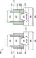
请参照图3-图12,其显示根据图2的方法200所制作的半导体元件300的工艺剖面图。半导体元件300包括NMOS鳍式场效应晶体管元件302及PMOS鳍式场效应晶体管元件304。应注意的是,部分的半导体元件300可以CMOS技术工艺流程制作。因此,可了解的是,附加的工艺可在图2的方法200之前、期间、及之后提供,且一些其他的工艺在此将仅简要叙述。应注意的是,为了清楚且更佳地了解本发明的实施例,仅显示部分的NMOS鳍式场效应晶体管元件302及PMOS鳍式场效应晶体管元件304。半导体元件300可在栅极最后工艺(也称为栅极置换)中制作。再栅极最后工艺中,最初先形成虚置多晶硅栅极结构,并接着进行标准的CMOS工艺流程直到沉积层间介电层。在层间介电层上进行化学机械研磨以使虚置多晶硅栅极结构露出。可接着移除虚置多晶硅栅极结构,并以金属栅极结构作置换。Please refer to FIGS. 3-12 , which show cross-sectional process views of the
在图3中,所显示的半导体元件300经历一外延工艺后,形成NMOS鳍式场效应晶体管元件302的源极及漏极区的外延硅,且经历一外延工艺后,形成PMOS鳍式场效应晶体管元件304的源极及漏极区的外延硅锗(SiGe)。半导体元件300包括基底306,例如是结晶结构的块材硅基底。在其他实施例中,基底102可包括其他的元素半导体,例如锗,或者可包括化合物半导体,例如碳化硅(silicon carbide)、砷化镓(gallium arsenide)、砷化铟(indiumarsenide)、及/或磷化铟(indium phophide)。在一些其他实施例中,基底102包括绝缘层上覆硅(SOI)基底。绝缘层上覆硅基底可使用氧注入隔离法(separation by implantation ofoxygen,SIMOX)、晶片接合、及/或其他适合的方法而制作。In FIG. 3, the
鳍状结构308为NMOS鳍式场效应晶体管元件302而形成,而鳍状结构310为PMOS鳍式场效应晶体管元件304而形成。虽然在NMOS鳍式场效应晶体管元件302及PMOS鳍式场效应晶体管元件304中皆仅显示一鳍状结构,但可了解的是,每一元件中皆可形成多重的鳍状结构,如同图1所示。鳍状结构308及310可使用适合的工艺而制作,包括光刻及蚀刻工艺。光刻工艺可包括在基底306之上形成光致抗蚀剂层、对光致抗蚀剂层曝光一图案、进行后曝光烘烤工艺(post-exposure bake process)、以及对光致抗蚀剂显影以形成包含光致抗蚀剂的掩模元件(mask element)。可使用反应性离子蚀刻(RIE)及/或其他适合的工艺而蚀刻鳍状结构308及310。鳍状结构308及310可具有宽度介于约20纳米至约30纳米。可沉积一介电层并将之蚀刻成围绕鳍状结构308及310的浅沟槽绝缘(STI)结构312。
在一实施例中,可通过双重图案化光刻(double-patterning lithography,DPL)工艺而形成鳍状结构。双重图案化光刻工艺是一种在基底上建构图案的方法,其将图案划分成两个彼此间留白的图案。双重图案化光刻工艺允许改善的结构(例如是鳍状结构)密度。可使用许多双重图案化光刻工艺方法,包括双重曝光(例如,使用两个掩模装置)、邻接结构形成间隙壁,并移除结构以提供间隙壁的图案、光致抗蚀剂冻结(resist freezing)、及/或其他适合的工艺。In one embodiment, the fin structure may be formed by a double-patterning lithography (DPL) process. Double patterning lithography is a method of building a pattern on a substrate by dividing the pattern into two patterns with a space between them. The double patterning photolithography process allows for improved density of structures such as fin structures. A number of double patterning photolithographic process methods can be used, including double exposure (e.g., using two masking devices), formation of spacers adjacent to structures, and removal of structures to provide a pattern of spacers, resist freezing freezing), and/or other suitable processes.
栅极结构314及316分别形成于鳍状结构308及310的中间部分上。栅极结构314及316分别包括栅极介电层322及323。在一实施例中,栅极介电层322及323可包括界面层。界面层可包括氧化硅层(例如是热氧化或化学沉积的方式形成),其具有介于约

栅极结构314及316还可包括分别形成于栅极介电层322及323上的盖层324及325。盖层324及325包括TiN,其具有介于约至约
栅极结构314及316还包括通过适合的沉积工艺而分别在盖层324及325上形成多晶硅层326及327。例如,可在CVD工艺中使用硅烷(SiH4)、硅乙烷(Si2H6)、或二氯硅烷(SiCl2H4)为化学气体以形成多晶硅层326及327。多晶硅层326及327也可称作虚置多晶硅层,因如下所讨论,其将被金属栅极电极取代。多晶硅层326及327可包括介于约

栅极结构314及316还可包括分别形成于多晶硅层326及327上的硬掩模层328及329。硬掩模层328及329可包括氧化硅、氮化硅、氮氧化硅、碳化硅、及/或其他适合的介电材料,且可使用例如是CVD或PVD的方法形成。硬掩模层328及329可包括介于约

一种图案化各种材料层以形成栅极结构314及316的方法在此揭示。在沉积多晶硅层之后,对多晶硅层进行化学机械研磨以将多晶硅层平坦化。在平坦化的多晶硅层上形成硬掩模层。通过适合的工艺在硬掩模层上形成光致抗蚀剂层,例如旋转涂布(spin-on coating),以及接着通过适当的光刻图案化方法将光致抗蚀剂层图案化为图案化光致抗蚀剂结构(patterned photoresistfeature)。图案化光致抗蚀剂层形成于硬掩模层之上。光致抗蚀剂层的图案转移至硬掩模层上,且接着转移至其他材料层以形成栅极结构314及316。浅沟槽绝缘层312可在图案化栅极结构314及316时作为蚀刻停止层。A method of patterning various material layers to form
栅极结构314及316还可包括设置于栅极结构的侧壁上的密封间隙壁332及333。密封间隙壁332及333可由氧化硅或其他适合的介电材料形成。密封间隙壁332及333可通过沉积介电材料层,并干蚀刻介电材料层而形成。可进行注入工艺以在NMOS鳍式场效应晶体管元件302中形成n型的浅掺杂源极/漏极区(即,nLDD),及在PMOS鳍式场效应晶体管元件304中形成p型的浅掺杂源极/漏极区(即,pLDD)。栅极结构314及316还可包括分别设置于密封间隙壁323及333上的虚置间隙壁334及335。虚置间隙壁334及335可包括多层结构,例如氮化硅及氧化硅。虚置间隙壁334及335可通过沉积氮化硅层及氧化硅层,并干蚀刻这些材料层而形成。The
进行一工艺以在栅极结构314的两侧上的鳍状结构308的露出部分上成长外延硅336。外延硅336的形成没有在鳍状结构308中蚀刻凹陷。此外,进行一工艺以在栅极结构316的两侧上的鳍状结构310的露出部分上成长外延硅锗(SiGe)338。形成保护层以在蚀刻PMOS鳍式场效应晶体管元件304的鳍状结构310的露出部分时保护NMOS鳍式场效应晶体管元件302。凹陷可通过干式蚀刻、湿式蚀刻、或前述的组合而形成。例如,干式蚀刻移除鳍状结构310的未被保护或露出的部分。在一些实施例中,可进行预清理工艺(pre-cleaning process)而使用HF或其他适合的溶液清理凹陷。可在外延硅336中掺杂n型掺质(dpants)(例如,磷或砷)以形成NMOS鳍式场效应晶体管元件302的源极及漏极区(S/D)。在其他实施例中,可使用外延SiC取代NMOS鳍式场效应晶体管元件302中的外延硅。可在外延硅锗338中掺杂p型掺质(dpants)(例如,硼)以形成PMOS鳍式场效应晶体管元件304的源极及漏极区(S/D)。在一些实施例中,在注入n型及p型掺质前,可形成主要间隙壁(mainspacers)来取代虚置间隙壁334及335。A process is performed to grow
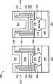
在图4中,半导体元件300还包括设置于NMOS鳍式场效应晶体管元件302中的外延硅336的源极及漏极区(S/D)上及设置于PMOS鳍式场效应晶体管元件304中的外延硅锗338的源极及漏极区(S/D)上的硅化结构(silicidefeatures)340。在一些实施例中,硅化结构340可通过硅化工艺(silicidation)而形成,例如是自对准硅化,其中在包含紧邻外延硅336及外延硅锗338的基底上形成金属材料,接着提升温度以进行退火,并造成下方的硅与金属之间产生反应以形成硅化物,及将未反应的金属蚀刻移除。硅化结构340可自对准并形成于NMOS鳍式场效应晶体管元件302及PMOS鳍式场效应晶体管元件304的源极及漏极区上以减低接触电阻。应注意的是,硬掩模层328及329分别避免其下的栅极结构314及316中的多晶硅层326及327发生硅化。In FIG. 4, the
在图5中,在硅化工艺之后,通过蚀刻工艺自栅极结构314及316移除硬掩模层328及329。蚀刻工艺可包括干式蚀刻、湿式蚀刻、或前述的组合。In FIG. 5, after the silicidation process, the hard mask layers 328 and 329 are removed from the
在图6中,可在基底306上形成接触蚀刻停止层(未显示),其包括位于栅极结构314及316、硅化结构340、及浅沟槽绝缘结构312之上。此外,在基底306上形成层间介电层341。层间介电层341可包括由高深宽比工艺(high aspect ratio process,HARP)及/或高密度等离子体(HDP)沉积工艺所形成的氧化物。之后,可在层间介电层341上进行化学机械研磨工艺以对层间介电层341进行平坦化及抛光,直至栅极结构314及316中的多晶硅层326及327分别露出。In FIG. 6 , a contact etch stop layer (not shown) may be formed on
在图7中,形成图案化光致抗蚀剂层342以保护NMOS鳍式场效应晶体管元件302区。例如,光刻工艺可包括在基底上形成光致抗蚀剂层、对光致抗蚀剂层曝光一图案、进行后曝光烘烤工艺、以及显影光致抗蚀剂层以形成图案化光致抗蚀剂层342。In FIG. 7 , a patterned
在图8中,自栅极结构316移除多晶硅层327,因而形成沟槽344。多晶硅层327可通过湿式或干式蚀刻工艺而移除。例如,湿式蚀刻工艺可包括暴露于含氢氧化物的溶液(例如,氢氧化铵)、去离子水、及/或其他适合的蚀刻溶液之中。盖层325可作为蚀刻时的蚀刻停止层。In FIG. 8 ,
在图9中,通过剥除(stripping)或其他适合的技术移除图案化光致抗蚀剂层342。自栅极结构314部分移除多晶硅层326,因而型成沟槽346。多晶硅层326可通过湿式或干式蚀刻工艺而被部分移除。余留在栅极结构314中的多晶硅层326a可具有介于约1纳米至约100纳米的厚度。应注意的是,在蚀刻栅极结构314及316之前,余留的多晶硅层326a在沉积多晶硅层期间已被掺杂。因此,余留的多晶硅层326a为NMOS鳍式场效应晶体管元件302的栅极电极的导电层。因此,当前的工艺可视为混合的栅极最后工艺,因为部分的栅极电极形成于先栅极工艺(gate first process),而另一部分的栅极电极形成于栅极最后(gate last)工艺,以下将作讨论。In FIG. 9, patterned
在图10中,在基底306上形成功函数金属层348,其部分填充于沟槽344及346之中。在一实施例中,功函数金属层348包括p型功函数金属(p-metal)层,其可形成在部分的沟槽344及346之中。p型功函数金属层可通过ALD、PVD、CVD、或其他适合的工艺而形成。再者,p型功函数金属层可包括单层金属层或多层金属层,其具有足够高的有效功函数(effectivework function,EWF)值,而可在PMOS鳍式场效应晶体管元件304中适当地运行。p型功函数金属层可包括TiN层,其具有介于约10纳米至约200纳米的厚度,以及TaN层,其具有介于约10纳米至约200纳米的厚度。或者,p型功函数金属层可包括其他的材料,例如Ru、Mo、Al、WN、及/或前述的组合。应注意的是,在栅极结构314中位于余留的多晶硅层326a上的p型功函数金属层不会对NMOS鳍式场效应晶体管元件302造成不利的影响。In FIG. 10 , a work
在图11中,在基底306上形成填充金属层350以将沟槽344及346的剩余部分填满。在一实施例中,填充金属层350包括铝(Al)。可形成钛层以作为湿润层(wetting layer)。钛层可通过PVD或其他适合的工艺而形成。可在钛层上形成铝层以将沟槽344及346的剩余部分填满。铝层可通过CVD、PVD、或其他适合的工艺而形成。或者,填充金属层可包括铜(Cu)或钨(W)。In FIG. 11 , a
在图12中,进行化学机械研磨以将半导体元件300平坦化,并移除位于沟槽344及346之外的金属层。在化学机械研磨之后,部分的功函数金属层348a及348b与填充金属层350a及350b分别保留于沟槽344及346之中。因此,金属栅极分别形成于NMOS鳍式场效应晶体管元件302及PMOS鳍式场效应晶体管元件304的栅极结构314及316之中。应了解的是,半导体元件300可经历进一步的工艺以完成制作。例如,在基底上形成多层内连线(multilayer interconnection,MLI),包括金属层(例如,M1、M2等)及金属间介电层(IMD),以电性连接许多元件结构而形成集成电路。多层内连线包括垂直内连线,例如现有的介层窗(vias)及接点(contacts),及水平内连线,例如金属线路。各种内连线结构可采用各种导电材料,包括铜、钨、及/或硅化物。在一实施例中,使用镶嵌工艺(damascene process)以形成多层内连线结构。In FIG. 12 , chemical mechanical polishing is performed to planarize the
请参照图13,其显示根据本发明另一实施例的方法400制作半导体元件的方法流程图。方法400开始于步骤402,提供具有第一区及第二区的基底。方法400继续进行至步骤404,在基底的第一区及第二区中分别形成第一及第二鳍状结构。方法400继续进行至步骤406,在第一及第二鳍状结构上分别形成第一及第二栅极结构。第一及第二栅极结构分别包括第一及第二多晶硅栅极。方法400继续进行至步骤408,在基底上形成层间介电层。方法400继续进行至步骤410,在层间介电层上进行化学机械研磨以使第一及第二多晶硅栅极露出。方法400继续进行至步骤412,部分移除第一及第二多晶硅栅极,因而在第一及第二栅极结构中分别形成第一及第二沟槽。Please refer to FIG. 13 , which shows a flowchart of a method for manufacturing a semiconductor device according to a
方法400继续进行至步骤414,形成掩模以保护第一栅极结构的第一多晶硅栅极的余留部分。方法400继续进行至步骤416,移除第二多晶硅栅极的余留部分,因而延伸了第二沟槽。方法400继续进行至步骤418,移除掩模。方法400继续进行至步骤420,形成功函数金属层,其部分填充第一及第二沟槽。方法400继续进行至步骤422,形成填充金属层,其填充第一及第二沟槽的余留部分。方法400继续进行至步骤424,移除位于第一及第二沟槽之外的金属层。以下将配合图14-图18讨论本发明实施例之中,可根据图13的方法400而制造的半导体元件。The
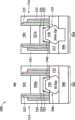
请参照图14-图18,其显示根据图13的方法400所制作的半导体元件500的工艺剖面图。除了以下将讨论的差异处,半导体元件500类似于半导体元件300。因此,为了简化与清楚化,图3-图12与图14-图18中的相似元件将采用相同的标号标示。应注意的是,部分的半导体元件500可以CMOS制作流程制造。因此,可了解的是,附加的工艺可在图13的方法400之前、期间、及之后提供,且一些其他的工艺在此将仅简要叙述。半导体元件500可经历与图3-图6的半导体元件300相同的工艺。图14显示半导体元件500处于与图6所示的半导体元件300相同的工艺阶段。多晶硅层326及327在于层间介电层341上进行化学机械研磨后露出。Please refer to FIGS. 14-18 , which show cross-sectional process views of the
在图15中,将多晶硅层326及327分别自栅极结构314及316部分移除,因而形成沟槽502及504。多晶硅层326及327可通过湿式或干式蚀刻工艺而部分移除。例如,湿式蚀刻工艺可包括暴露于含氢氧化物的溶液(例如,氢氧化铵)、去离子水、及/或其他适合的蚀刻溶液。栅极结构314及316中所余留的多晶硅层326a及327a可具有介于约5纳米至约50纳米的厚度。In FIG. 15 , polysilicon layers 326 and 327 are partially removed from
在图16中,形成图案化光致抗蚀剂层510以保护NMOS鳍式场效应晶体管元件302区。例如,光刻工艺可包括在基底上形成光致抗蚀剂层、对光致抗蚀剂层曝光一图案、进行后曝光烘烤工艺、及显影光致抗蚀剂以形成图案化光致抗蚀剂层510。In FIG. 16 , a patterned
在图17中,自栅极结构316移除余留的多晶硅栅极层327a,因而延伸了沟槽504。盖层325可用作蚀刻时的蚀刻停止层。应注意的是,在蚀刻栅极结构314及316之前,栅极结构314中余留的多晶硅层326a在沉积多晶硅层期间已被掺杂。因此,余留的多晶硅层326a为NMOS鳍式场效应晶体管元件302的栅极电极的导电层。因此,当前的工艺可视为混合的栅极最后工艺,因为部分的栅极电极形成于先栅极工艺(gate first process),而另一部分的栅极电极形成于栅极最后(gate last)工艺。In FIG. 17 , the remaining
在图18中,通过剥除(stripping)或其他适合的技术移除图案化光致抗蚀剂层510。半导体元件500可经历与图10-图12所讨论的相同的工艺以完成制作。在此所揭示的实施例中,应注意的是,在FinFET元件中以金属置换多晶硅层可增加PMOS/NMOS元件的沟道区上的SiGe/SiC应力。相较于平面的FET元件,FinFET元件,具有较高的金属栅极应力敏感度,这是因为FinFET元件的栅极弯绕结构(gate warp around configuration)。应力随着鳍状结构的宽度的减少而增加。再者,相较于在平面的FET元件中进行栅极最后工艺以置换多晶硅层,在FinFET元件中进行栅极最后工艺以置换多晶硅层是较不复杂的。In FIG. 18, patterned
虽然本发明已以多个较佳实施例公开如上,然其并非用以限定本发明,任何本领域普通技术人员,在不脱离本发明的精神和范围内,当可作任意的更动与润饰,因此本发明的保护范围当视所附的权利要求所界定的范围为准。Although the present invention has been disclosed above with a number of preferred embodiments, it is not intended to limit the present invention. Any person skilled in the art may make arbitrary changes and modifications without departing from the spirit and scope of the present invention. , so the scope of protection of the present invention should be based on the scope defined by the appended claims.
Claims (10)
Translated fromChineseApplications Claiming Priority (2)
| Application Number | Priority Date | Filing Date | Title |
|---|---|---|---|
| US12/756,662 | 2010-04-08 | ||
| US12/756,662US8609495B2 (en) | 2010-04-08 | 2010-04-08 | Hybrid gate process for fabricating finfet device |
Publications (2)
| Publication Number | Publication Date |
|---|---|
| CN102214579A CN102214579A (en) | 2011-10-12 |
| CN102214579Btrue CN102214579B (en) | 2013-04-24 |
Family
ID=44745838
Family Applications (1)
| Application Number | Title | Priority Date | Filing Date |
|---|---|---|---|
| CN201010568174.XAExpired - Fee RelatedCN102214579B (en) | 2010-04-08 | 2010-11-29 | Manufacturing method of semiconductor element and semiconductor element |
Country Status (2)
| Country | Link |
|---|---|
| US (2) | US8609495B2 (en) |
| CN (1) | CN102214579B (en) |
Families Citing this family (82)
| Publication number | Priority date | Publication date | Assignee | Title |
|---|---|---|---|---|
| US10238294B2 (en) | 2006-06-29 | 2019-03-26 | Accuvein, Inc. | Scanned laser vein contrast enhancer using one laser |
| US8153493B2 (en) | 2008-08-28 | 2012-04-10 | Taiwan Semiconductor Manufacturing Company, Ltd. | FinFET process compatible native transistor |
| US9245805B2 (en)* | 2009-09-24 | 2016-01-26 | Taiwan Semiconductor Manufacturing Company, Ltd. | Germanium FinFETs with metal gates and stressors |
| US8357569B2 (en) | 2009-09-29 | 2013-01-22 | Taiwan Semiconductor Manufacturing Company, Ltd. | Method of fabricating finfet device |
| US8415718B2 (en) | 2009-10-30 | 2013-04-09 | Taiwan Semiconductor Manufacturing Company, Ltd. | Method of forming epi film in substrate trench |
| CN101777564B (en)* | 2009-12-24 | 2011-06-15 | 中国科学院上海微系统与信息技术研究所 | SOI CMO device with vertical grid structure |
| US8310013B2 (en) | 2010-02-11 | 2012-11-13 | Taiwan Semiconductor Manufacturing Company, Ltd. | Method of fabricating a FinFET device |
| US8942030B2 (en) | 2010-06-25 | 2015-01-27 | Taiwan Semiconductor Manufacturing Company, Ltd. | Structure and method for SRAM cell circuit |
| US8212295B2 (en) | 2010-06-30 | 2012-07-03 | Taiwan Semiconductor Manufacturing Company, Ltd. | ROM cell circuit for FinFET devices |
| US8609495B2 (en) | 2010-04-08 | 2013-12-17 | Taiwan Semiconductor Manufacturing Company, Ltd. | Hybrid gate process for fabricating finfet device |
| US8653610B2 (en) | 2010-04-21 | 2014-02-18 | International Business Machines Corporation | High performance non-planar semiconductor devices with metal filled inter-fin gaps |
| US8796759B2 (en) | 2010-07-15 | 2014-08-05 | Taiwan Semiconductor Manufacturing Company, Ltd. | Fin-like field effect transistor (FinFET) device and method of manufacturing same |
| US8858818B2 (en)* | 2010-09-30 | 2014-10-14 | Suvolta, Inc. | Method for minimizing defects in a semiconductor substrate due to ion implantation |
| KR101815527B1 (en)* | 2010-10-07 | 2018-01-05 | 삼성전자주식회사 | Semiconductor device and method for manufacturing the same |
| US8062963B1 (en) | 2010-10-08 | 2011-11-22 | Taiwan Semiconductor Manufacturing Company, Ltd. | Method of fabricating a semiconductor device having an epitaxy region |
| US9472550B2 (en) | 2010-11-23 | 2016-10-18 | Taiwan Semiconductor Manufacturing Company, Ltd. | Adjusted fin width in integrated circuitry |
| DE102011004506B4 (en)* | 2011-02-22 | 2012-10-18 | Globalfoundries Dresden Module One Limited Liability Company & Co. Kg | A method of fabricating a semiconductor device and semiconductor device as a fin transistor fabricated on a patterned STI region by a late stage etch |
| US8796124B2 (en) | 2011-10-25 | 2014-08-05 | Taiwan Semiconductor Manufacturing Company, Ltd. | Doping method in 3D semiconductor device |
| CN103094208B (en)* | 2011-10-31 | 2015-04-01 | 中芯国际集成电路制造(上海)有限公司 | Manufacturing method of transistor |
| CN103177944B (en)* | 2011-12-20 | 2015-12-16 | 中芯国际集成电路制造(上海)有限公司 | Make the method for semiconductor device |
| US9087687B2 (en) | 2011-12-23 | 2015-07-21 | International Business Machines Corporation | Thin heterostructure channel device |
| CN104160507B (en)* | 2011-12-28 | 2017-10-24 | 英特尔公司 | Method for Integrating Multiple Gate Dielectric Transistors on a Tri-Gate (FINFET) Process |
| KR101876793B1 (en)* | 2012-02-27 | 2018-07-11 | 삼성전자주식회사 | Field Effect Transistor and Method of fabricating the same |
| KR20130116099A (en)* | 2012-04-13 | 2013-10-23 | 삼성전자주식회사 | Semiconductor device and method for fabricating the same |
| US9171929B2 (en) | 2012-04-25 | 2015-10-27 | Taiwan Semiconductor Manufacturing Company, Ltd. | Strained structure of semiconductor device and method of making the strained structure |
| US8778786B1 (en) | 2012-05-29 | 2014-07-15 | Suvolta, Inc. | Method for substrate preservation during transistor fabrication |
| US8946063B2 (en)* | 2012-11-30 | 2015-02-03 | International Business Machines Corporation | Semiconductor device having SSOI substrate with relaxed tensile stress |
| US9064857B2 (en)* | 2012-12-19 | 2015-06-23 | Taiwan Semiconductor Manufacturing Company, Ltd. | N metal for FinFET |
| US9859429B2 (en)* | 2013-01-14 | 2018-01-02 | Taiwan Semiconductor Manufacturing Company, Ltd. | FinFET device and method of fabricating same |
| KR102049774B1 (en)* | 2013-01-24 | 2019-11-28 | 삼성전자 주식회사 | Semiconductor device and fabricated method thereof |
| KR102067171B1 (en) | 2013-02-14 | 2020-01-16 | 삼성전자주식회사 | A semiconductor device and method of fabricating the same |
| US8912063B2 (en) | 2013-03-14 | 2014-12-16 | Samsung Electronics Co., Ltd. | Semiconductor device having blocking pattern and method for fabricating the same |
| US9087724B2 (en)* | 2013-03-21 | 2015-07-21 | International Business Machines Corporation | Method and structure for finFET CMOS |
| US9059217B2 (en) | 2013-03-28 | 2015-06-16 | International Business Machines Corporation | FET semiconductor device with low resistance and enhanced metal fill |
| CN103413758B (en)* | 2013-07-17 | 2017-02-08 | 华为技术有限公司 | Manufacturing method for semiconductor fin ray and manufacturing method for FinFET device |
| US9293586B2 (en) | 2013-07-17 | 2016-03-22 | Globalfoundries Inc. | Epitaxial block layer for a fin field effect transistor device |
| US9159794B2 (en)* | 2014-01-16 | 2015-10-13 | Globalfoundries Inc. | Method to form wrap-around contact for finFET |
| US9343412B2 (en) | 2014-02-12 | 2016-05-17 | Taiwan Semiconductor Manufacturing Company Limited | Method of forming MOSFET structure |
| CN103871897A (en)* | 2014-02-21 | 2014-06-18 | 上海华力微电子有限公司 | Chemical mechanical grinding method applied to FinFET (fin field-effect transistor) structure |
| US9059311B1 (en) | 2014-03-05 | 2015-06-16 | International Business Machines Corporation | CMOS transistors with identical active semiconductor region shapes |
| US10163652B2 (en) | 2014-03-13 | 2018-12-25 | Taiwan Semiconductor Manufacturing Company, Ltd. | Mechanisms for forming patterns using multiple lithography processes |
| KR102178831B1 (en) | 2014-03-13 | 2020-11-13 | 삼성전자 주식회사 | Method of forming semiconductor device having stressor and related device |
| US9761436B2 (en) | 2014-06-30 | 2017-09-12 | Taiwan Semiconductor Manufacturing Company, Ltd. | Mechanisms for forming patterns using multiple lithography processes |
| US9105475B1 (en)* | 2014-03-18 | 2015-08-11 | Tsinghua University | Method for forming fin field effect transistor |
| WO2015147783A1 (en)* | 2014-03-24 | 2015-10-01 | Intel Corporation | Techniques for achieving multiple transistor fin dimensions on a single die |
| US9653461B2 (en) | 2014-03-28 | 2017-05-16 | Taiwan Semiconductor Manufacturing Company, Ltd. | FinFETs with low source/drain contact resistance |
| US9209095B2 (en)* | 2014-04-04 | 2015-12-08 | International Business Machines Corporation | III-V, Ge, or SiGe fin base lateral bipolar transistor structure and method |
| US10700170B2 (en)* | 2014-04-29 | 2020-06-30 | Globalfoundries Inc. | Multiple fin finFET with low-resistance gate structure |
| US9490365B2 (en)* | 2014-06-12 | 2016-11-08 | Taiwan Semiconductor Manufacturing Co., Ltd. | Structure and formation method of fin-like field effect transistor |
| US9502538B2 (en) | 2014-06-12 | 2016-11-22 | Taiwan Semiconductor Manufacturing Co., Ltd | Structure and formation method of fin-like field effect transistor |
| US9735153B2 (en)* | 2014-07-14 | 2017-08-15 | Samsung Electronics Co., Ltd. | Semiconductor device having fin-type field effect transistor and method of manufacturing the same |
| CN105304490B (en)* | 2014-07-23 | 2020-09-15 | 联华电子股份有限公司 | Method of making a semiconductor structure |
| US10056462B2 (en)* | 2014-08-13 | 2018-08-21 | Taiwan Semiconductor Manufacturing Company Ltd. | Metal gate structure and manufacturing method thereof |
| US9385197B2 (en) | 2014-08-29 | 2016-07-05 | Taiwan Semiconductor Manufacturing Co., Ltd | Semiconductor structure with contact over source/drain structure and method for forming the same |
| CN105470295B (en)* | 2014-09-09 | 2020-06-30 | 联华电子股份有限公司 | Fin structure and manufacturing method thereof |
| US9324820B1 (en) | 2014-10-28 | 2016-04-26 | Taiwan Semiconductor Manufacturing Co., Ltd | Method for forming semiconductor structure with metallic layer over source/drain structure |
| KR102217246B1 (en)* | 2014-11-12 | 2021-02-18 | 삼성전자주식회사 | Integrated circuit device and method of manufacturing the same |
| KR102168302B1 (en)* | 2014-11-21 | 2020-10-22 | 삼성전자주식회사 | Semiconductor device using three dimensional channel |
| US9780214B2 (en)* | 2014-12-22 | 2017-10-03 | Taiwan Semiconductor Manufacturing Co., Ltd. | Semiconductor device including Fin- FET and manufacturing method thereof |
| KR102287398B1 (en) | 2015-01-14 | 2021-08-06 | 삼성전자주식회사 | Semiconductor device |
| KR102312346B1 (en) | 2015-02-23 | 2021-10-14 | 삼성전자주식회사 | Methods of Fabricating Semiconductor Devices |
| US9711369B2 (en) | 2015-03-16 | 2017-07-18 | Taiwan Semiconductor Manufacturing Company, Ltd. | Method for forming patterns with sharp jogs |
| US10043802B2 (en) | 2015-04-17 | 2018-08-07 | Taiwan Semiconductor Manufacturing Co., Ltd. | Gate structure with additional oxide layer |
| US9583485B2 (en) | 2015-05-15 | 2017-02-28 | Taiwan Semiconductor Manufacturing Company, Ltd. | Fin field effect transistor (FinFET) device structure with uneven gate structure and method for forming the same |
| US9818841B2 (en) | 2015-05-15 | 2017-11-14 | Taiwan Semiconductor Manufacturing Co., Ltd. | Semiconductor structure with unleveled gate structure and method for forming the same |
| US9660084B2 (en) | 2015-07-01 | 2017-05-23 | Taiwan Semiconductor Manufacturing Company, Ltd. | Semiconductor device structure and method for forming the same |
| US9698101B2 (en) | 2015-08-28 | 2017-07-04 | International Business Machines Corporation | Self-aligned local interconnect technology |
| KR102323943B1 (en) | 2015-10-21 | 2021-11-08 | 삼성전자주식회사 | Method of manufacturing semiconductor device |
| US9960273B2 (en)* | 2015-11-16 | 2018-05-01 | Taiwan Semiconductor Manufacturing Company, Ltd. | Integrated circuit structure with substrate isolation and un-doped channel |
| US20170141228A1 (en)* | 2015-11-16 | 2017-05-18 | Taiwan Semiconductor Manufacturing Co., Ltd. | Field effect transistor and manufacturing method thereof |
| KR102449211B1 (en)* | 2016-01-05 | 2022-09-30 | 삼성전자주식회사 | Semiconductor devices including field effect transistors |
| KR102526580B1 (en)* | 2016-01-11 | 2023-04-27 | 삼성전자주식회사 | Semiconductor devices and methods of manufacturing the same |
| TWI692871B (en)* | 2016-08-03 | 2020-05-01 | 聯華電子股份有限公司 | Semiconductor structure and its manufacturing method |
| CN107785321A (en)* | 2016-08-26 | 2018-03-09 | 中芯国际集成电路制造(上海)有限公司 | The manufacture method of semiconductor structure |
| USD834133S1 (en) | 2017-06-07 | 2018-11-20 | Steiner Eoptics, Inc. | Dual beam aiming laser |
| CN109309055B (en)* | 2017-07-26 | 2021-04-02 | 中芯国际集成电路制造(上海)有限公司 | Semiconductor structure and method of forming the same |
| US10636893B2 (en) | 2018-08-22 | 2020-04-28 | Globalfoundries Inc. | Replacement metal gate with reduced shorting and uniform chamfering |
| US10872826B2 (en)* | 2018-10-31 | 2020-12-22 | Taiwan Semiconductor Manufacturing Company, Ltd. | Fin field-effect transistor device and method |
| US11282934B2 (en)* | 2019-07-26 | 2022-03-22 | Taiwan Semiconductor Manufacturing Co., Ltd. | Structure for metal gate electrode and method of fabrication |
| US11081396B2 (en) | 2019-09-12 | 2021-08-03 | Taiwan Semiconductor Manufacturing Company, Ltd. | Semiconductor device and method |
| US11295989B2 (en)* | 2020-05-26 | 2022-04-05 | Taiwan Semiconductor Manufacturing Co., Ltd. | Gate structures for semiconductor devices |
| US11335683B2 (en)* | 2020-06-30 | 2022-05-17 | Qualcomm Incorporated | Device channel profile structure |
Citations (3)
| Publication number | Priority date | Publication date | Assignee | Title |
|---|---|---|---|---|
| US6929992B1 (en)* | 2003-12-17 | 2005-08-16 | Advanced Micro Devices, Inc. | Strained silicon MOSFETs having NMOS gates with work functions for compensating NMOS threshold voltage shift |
| CN101192605A (en)* | 2006-11-30 | 2008-06-04 | 国际商业机器公司 | Semiconductor device and manufacturing method thereof |
| CN101414632A (en)* | 2007-10-16 | 2009-04-22 | 台湾积体电路制造股份有限公司 | Fin field effect transistor |
Family Cites Families (52)
| Publication number | Priority date | Publication date | Assignee | Title |
|---|---|---|---|---|
| US7358121B2 (en) | 2002-08-23 | 2008-04-15 | Intel Corporation | Tri-gate devices and methods of fabrication |
| US6706571B1 (en) | 2002-10-22 | 2004-03-16 | Advanced Micro Devices, Inc. | Method for forming multiple structures in a semiconductor device |
| US6864519B2 (en)* | 2002-11-26 | 2005-03-08 | Taiwan Semiconductor Manufacturing Co., Ltd. | CMOS SRAM cell configured using multiple-gate transistors |
| US6764884B1 (en)* | 2003-04-03 | 2004-07-20 | Advanced Micro Devices, Inc. | Method for forming a gate in a FinFET device and thinning a fin in a channel region of the FinFET device |
| US6943407B2 (en)* | 2003-06-17 | 2005-09-13 | International Business Machines Corporation | Low leakage heterojunction vertical transistors and high performance devices thereof |
| KR100513405B1 (en) | 2003-12-16 | 2005-09-09 | 삼성전자주식회사 | Method for forming fin field effect transistor |
| US7247578B2 (en)* | 2003-12-30 | 2007-07-24 | Intel Corporation | Method of varying etch selectivities of a film |
| US7154118B2 (en)* | 2004-03-31 | 2006-12-26 | Intel Corporation | Bulk non-planar transistor having strained enhanced mobility and methods of fabrication |
| US7244640B2 (en) | 2004-10-19 | 2007-07-17 | Taiwan Semiconductor Manufacturing Company, Ltd. | Method for fabricating a body contact in a Finfet structure and a device including the same |
| US7195969B2 (en)* | 2004-12-31 | 2007-03-27 | Taiwan Semiconductor Manufacturing Co., Ltd. | Strained channel CMOS device with fully silicided gate electrode |
| JP5015446B2 (en)* | 2005-05-16 | 2012-08-29 | アイメック | Method for forming double fully silicided gates and device obtained by said method |
| US7858481B2 (en)* | 2005-06-15 | 2010-12-28 | Intel Corporation | Method for fabricating transistor with thinned channel |
| US8466490B2 (en) | 2005-07-01 | 2013-06-18 | Synopsys, Inc. | Enhanced segmented channel MOS transistor with multi layer regions |
| US7265008B2 (en) | 2005-07-01 | 2007-09-04 | Synopsys, Inc. | Method of IC production using corrugated substrate |
| US7605449B2 (en) | 2005-07-01 | 2009-10-20 | Synopsys, Inc. | Enhanced segmented channel MOS transistor with high-permittivity dielectric isolation material |
| US7247887B2 (en) | 2005-07-01 | 2007-07-24 | Synopsys, Inc. | Segmented channel MOS transistor |
| US7508031B2 (en) | 2005-07-01 | 2009-03-24 | Synopsys, Inc. | Enhanced segmented channel MOS transistor with narrowed base regions |
| US7807523B2 (en) | 2005-07-01 | 2010-10-05 | Synopsys, Inc. | Sequential selective epitaxial growth |
| US7190050B2 (en) | 2005-07-01 | 2007-03-13 | Synopsys, Inc. | Integrated circuit on corrugated substrate |
| US7229873B2 (en)* | 2005-08-10 | 2007-06-12 | Texas Instruments Incorporated | Process for manufacturing dual work function metal gates in a microelectronics device |
| US7485536B2 (en)* | 2005-12-30 | 2009-02-03 | Intel Corporation | Abrupt junction formation by atomic layer epitaxy of in situ delta doped dopant diffusion barriers |
| US8304342B2 (en)* | 2006-10-31 | 2012-11-06 | Texas Instruments Incorporated | Sacrificial CMP etch stop layer |
| US7781288B2 (en)* | 2007-02-21 | 2010-08-24 | International Business Machines Corporation | Semiconductor structure including gate electrode having laterally variable work function |
| JP2008227277A (en)* | 2007-03-14 | 2008-09-25 | Nec Electronics Corp | Manufacturing method of semiconductor device |
| US7898037B2 (en) | 2007-04-18 | 2011-03-01 | Taiwan Semiconductor Manufacturing Company, Ltd. | Contact scheme for MOSFETs |
| US7939862B2 (en) | 2007-05-30 | 2011-05-10 | Synopsys, Inc. | Stress-enhanced performance of a FinFet using surface/channel orientations and strained capping layers |
| US8883597B2 (en) | 2007-07-31 | 2014-11-11 | Taiwan Semiconductor Manufacturing Company, Ltd. | Method of fabrication of a FinFET element |
| US7776680B2 (en)* | 2008-01-03 | 2010-08-17 | International Business Machines Corporation | Complementary metal oxide semiconductor device with an electroplated metal replacement gate |
| US8536660B2 (en)* | 2008-03-12 | 2013-09-17 | Taiwan Semiconductor Manufacturing Company, Ltd. | Hybrid process for forming metal gates of MOS devices |
| US7838366B2 (en)* | 2008-04-11 | 2010-11-23 | United Microelectronics Corp. | Method for fabricating a metal gate structure |
| US8283231B2 (en) | 2008-06-11 | 2012-10-09 | Taiwan Semiconductor Manufacturing Company, Ltd. | finFET drive strength modification |
| US7910453B2 (en) | 2008-07-14 | 2011-03-22 | Taiwan Semiconductor Manufacturing Company, Ltd. | Storage nitride encapsulation for non-planar sonos NAND flash charge retention |
| US8153493B2 (en) | 2008-08-28 | 2012-04-10 | Taiwan Semiconductor Manufacturing Company, Ltd. | FinFET process compatible native transistor |
| US8153498B2 (en)* | 2008-08-29 | 2012-04-10 | Taiwan Semiconductor Manufacturing Company, Ltd. | Downsize polysilicon height for polysilicon resistor integration of replacement gate process |
| US8084824B2 (en)* | 2008-09-11 | 2011-12-27 | United Microelectronics Corp. | Metal gate transistor and method for fabricating the same |
| US7977181B2 (en)* | 2008-10-06 | 2011-07-12 | Taiwan Semiconductor Manufacturing Company, Ltd. | Method for gate height control in a gate last process |
| US7989355B2 (en) | 2009-02-12 | 2011-08-02 | Taiwan Semiconductor Manufacturing Company, Ltd. | Method of pitch halving |
| US7862962B2 (en) | 2009-01-20 | 2011-01-04 | Taiwan Semiconductor Manufacturing Company, Ltd. | Integrated circuit layout design |
| US8053299B2 (en) | 2009-04-17 | 2011-11-08 | Taiwan Semiconductor Manufacturing Company, Ltd. | Method of fabrication of a FinFET element |
| US8890260B2 (en)* | 2009-09-04 | 2014-11-18 | Taiwan Semiconductor Manufacturing Company, Ltd. | Polysilicon design for replacement gate technology |
| US7985639B2 (en)* | 2009-09-18 | 2011-07-26 | GlobalFoundries, Inc. | Method for fabricating a semiconductor device having a semiconductive resistor structure |
| US8455859B2 (en)* | 2009-10-01 | 2013-06-04 | Taiwan Semiconductor Manufacturing Company, Ltd. | Strained structure of semiconductor device |
| US8343872B2 (en)* | 2009-11-06 | 2013-01-01 | Taiwan Semiconductor Manufacturing Company, Ltd. | Method of forming strained structures with compound profiles in semiconductor devices |
| US8765556B2 (en)* | 2009-12-23 | 2014-07-01 | Taiwan Semiconductor Manufacturing Company, Ltd. | Method of fabricating strained structure in semiconductor device |
| US20110147840A1 (en)* | 2009-12-23 | 2011-06-23 | Cea Stephen M | Wrap-around contacts for finfet and tri-gate devices |
| US8093117B2 (en)* | 2010-01-14 | 2012-01-10 | Taiwan Semiconductor Manufacturing Company, Ltd. | Method of forming a metal gate |
| US8609497B2 (en)* | 2010-02-12 | 2013-12-17 | Taiwan Semiconductor Manufacturing Company, Ltd. | Method of dual EPI process for semiconductor device |
| US8466034B2 (en)* | 2010-03-29 | 2013-06-18 | GlobalFoundries, Inc. | Method of manufacturing a finned semiconductor device structure |
| US8609495B2 (en) | 2010-04-08 | 2013-12-17 | Taiwan Semiconductor Manufacturing Company, Ltd. | Hybrid gate process for fabricating finfet device |
| US8354313B2 (en)* | 2010-04-30 | 2013-01-15 | International Business Machines Corporation | Method to optimize work function in complementary metal oxide semiconductor (CMOS) structures |
| JP5569243B2 (en)* | 2010-08-09 | 2014-08-13 | ソニー株式会社 | Semiconductor device and manufacturing method thereof |
| US8563374B2 (en)* | 2011-09-16 | 2013-10-22 | GlobalFoundries, Inc. | Strained semiconductor devices having asymmetrical heterojunction structures and methods for the fabrication thereof |
- 2010
- 2010-04-08USUS12/756,662patent/US8609495B2/ennot_activeExpired - Fee Related
- 2010-11-29CNCN201010568174.XApatent/CN102214579B/ennot_activeExpired - Fee Related
- 2013
- 2013-11-19USUS14/083,533patent/US8994116B2/enactiveActive
Patent Citations (3)
| Publication number | Priority date | Publication date | Assignee | Title |
|---|---|---|---|---|
| US6929992B1 (en)* | 2003-12-17 | 2005-08-16 | Advanced Micro Devices, Inc. | Strained silicon MOSFETs having NMOS gates with work functions for compensating NMOS threshold voltage shift |
| CN101192605A (en)* | 2006-11-30 | 2008-06-04 | 国际商业机器公司 | Semiconductor device and manufacturing method thereof |
| CN101414632A (en)* | 2007-10-16 | 2009-04-22 | 台湾积体电路制造股份有限公司 | Fin field effect transistor |
Also Published As
| Publication number | Publication date |
|---|---|
| US8994116B2 (en) | 2015-03-31 |
| CN102214579A (en) | 2011-10-12 |
| US20110248348A1 (en) | 2011-10-13 |
| US20140061817A1 (en) | 2014-03-06 |
| US8609495B2 (en) | 2013-12-17 |
Similar Documents
| Publication | Publication Date | Title |
|---|---|---|
| CN102214579B (en) | Manufacturing method of semiconductor element and semiconductor element | |
| US12159913B2 (en) | Contact structures for gate-all-around devices and methods of forming the same | |
| CN110556374B (en) | FinFET device structure and method with contacts over dielectric gate | |
| CN103811550B (en) | The contact structures of semiconductor device | |
| US9337304B2 (en) | Method of making semiconductor device | |
| KR101745793B1 (en) | Semiconductor device having a plurality of fins and method for fabricating the same | |
| KR101334465B1 (en) | Improved silicide formation and associated devices | |
| KR101455478B1 (en) | Contact structure of semiconductor device | |
| US9397097B2 (en) | Gate structure for semiconductor device | |
| CN103187418B (en) | A kind of CMOS FinFET and forming method thereof | |
| CN103050530B (en) | FinFET device and method of manufacturing same | |
| TWI419236B (en) | Fin field effect transistor component manufacturing method | |
| US9685439B1 (en) | Semiconductor device and manufacturing method thereof | |
| US20150115372A1 (en) | Metal gate finfet device | |
| US12159924B2 (en) | Structure and method for multigate devices with suppressed diffusion | |
| TW201903858A (en) | Semiconductor device manufacturing method | |
| US20180019242A1 (en) | Semiconductor device and manufacturing method thereof | |
| TWI801923B (en) | Semiconductor device and method of manufacture | |
| TW202119628A (en) | Semiconductor structure | |
| TWI795774B (en) | Gapfill structure and manufacturing methods thereof |
Legal Events
| Date | Code | Title | Description |
|---|---|---|---|
| C06 | Publication | ||
| PB01 | Publication | ||
| C10 | Entry into substantive examination | ||
| SE01 | Entry into force of request for substantive examination | ||
| C14 | Grant of patent or utility model | ||
| GR01 | Patent grant | ||
| CF01 | Termination of patent right due to non-payment of annual fee | Granted publication date:20130424 | |
| CF01 | Termination of patent right due to non-payment of annual fee |