CN102214158B - A Dynamically Reconfigurable Processor with Fully Interconnected Routing Structure - Google Patents
A Dynamically Reconfigurable Processor with Fully Interconnected Routing StructureDownload PDFInfo
- Publication number
- CN102214158B CN102214158BCN 201110152238CN201110152238ACN102214158BCN 102214158 BCN102214158 BCN 102214158BCN 201110152238CN201110152238CN 201110152238CN 201110152238 ACN201110152238 ACN 201110152238ACN 102214158 BCN102214158 BCN 102214158B
- Authority
- CN
- China
- Prior art keywords
- reconfigurable
- array module
- module
- connecting valve
- interconnected
- Prior art date
- Legal status (The legal status is an assumption and is not a legal conclusion. Google has not performed a legal analysis and makes no representation as to the accuracy of the status listed.)
- Active
Links
Images


Landscapes
- Memory System Of A Hierarchy Structure (AREA)
- Multi Processors (AREA)
Abstract
Description
Translated fromChinese技术领域technical field
本发明涉及动态可重构处理器领域,特别涉及一种全互联路由结构动态可重构处理器。 The invention relates to the field of dynamically reconfigurable processors, in particular to a dynamic reconfigurable processor with a fully interconnected routing structure. the
背景技术Background technique
可重构计算是一种将软件的灵活性和硬件的高效性结合在一起的计算方式,比如现场可编程逻辑门阵列(Field Programmable Gate Array,FPGA)就是一个可重构计算应用的具体实例。和普通微处理器之间的区别在于它不仅可以改变控制流,还可以改变数据通路(Data Path)的结构,具有高性能、低硬件开销和功耗、灵活性好、扩展性好的优点。目前主要应用于媒体处理、模式识别、基带处理等计算密集型的算法。随着嵌入式处理器普遍要求缩短设计周期、降低设计和开发成本,另外最终市场和技术的不确定性越来越大,可重构处理逐步成为嵌入式处理器国际发展的趋势。不仅如此,在很多高性能计算的领域它也有所涉足,包括结构分析、计算流体力学、分子模拟、生物信息、计算化学、地震地质(油气勘探)、数值气象、宇宙学研究等。 Reconfigurable computing is a computing method that combines the flexibility of software and the efficiency of hardware. For example, Field Programmable Gate Array (Field Programmable Gate Array, FPGA) is a specific example of reconfigurable computing applications. The difference between it and ordinary microprocessors is that it can not only change the control flow, but also change the structure of the data path (Data Path), which has the advantages of high performance, low hardware overhead and power consumption, good flexibility and good scalability. At present, it is mainly used in computing-intensive algorithms such as media processing, pattern recognition, and baseband processing. As embedded processors generally require shortening the design cycle, reducing design and development costs, and the uncertainty of the final market and technology is increasing, reconfigurable processing has gradually become the international development trend of embedded processors. Not only that, it has also been involved in many high-performance computing fields, including structural analysis, computational fluid dynamics, molecular simulation, bioinformatics, computational chemistry, seismic geology (oil and gas exploration), numerical meteorology, and cosmology research. the
新的半导体工艺为可重构硬件带来千万门级电路的技术,从而为可重构硬件提供足够的面积;在速度上,可重构硬件的性能正在接近专用定制芯片。在这些变化影响下,可重构计算在技术路线上逐步走上动态重构、粗颗粒度并行硬件、异构多核的道路。例如欧洲微电子中心(IMEC)的ADRES处理器由紧耦合的超长指令字(Very Long Instruction Word,VLIW)处理器内核和粗颗粒度并行矩阵计算的可重构硬件构成。而惠普(HP)的CHESS处理器则由大量可重构算术可重构阵列模块构成。 The new semiconductor process brings tens of millions of gate-level circuit technology to reconfigurable hardware, thereby providing sufficient area for reconfigurable hardware; in terms of speed, the performance of reconfigurable hardware is approaching dedicated custom chips. Under the influence of these changes, reconfigurable computing has gradually embarked on the road of dynamic reconfiguration, coarse-grained parallel hardware, and heterogeneous multi-core on the technical route. For example, the ADRES processor of the European Microelectronics Center (IMEC) is composed of a tightly coupled Very Long Instruction Word (VLIW) processor core and reconfigurable hardware for coarse-grained parallel matrix computing. And Hewlett-Packard (HP)'s CHESS processor is made up of a large number of reconfigurable arithmetic reconfigurable array modules. the
可重构处理器的基本组成包括主控制器和可重构运算单元。可重构运算单元均采用阵列的形式(阵列是并行化硬件的基本形式),来加大处理能力,同时通过灵活的互联结果来保证阵列的通用性。运算单元之间动态可重构的互联是动态可重构处理器芯片实现的关键技术之一。 The basic composition of a reconfigurable processor includes a main controller and a reconfigurable computing unit. The reconfigurable computing units are all in the form of arrays (arrays are the basic form of parallel hardware) to increase processing capabilities, and at the same time ensure the versatility of the arrays through flexible interconnection results. Dynamically reconfigurable interconnection between computing units is one of the key technologies for the realization of dynamically reconfigurable processor chips. the
互联结构需要保证阵列灵活性的同时,考虑外部连接开关带宽,提高芯片的计算吞吐量。现有的互联结构,有的采取FPGA中connecting-box和switching-box的结构,非常灵活,但问题在于配置点过多,重构的信息量过大,导致无法动态完成,降低面积利用效率,限制了应用范围(比如嵌入式)。动态可重构阵列模块中也有使用NoC上的mesh全互联结构和传输协议包的形式:Mesh全互联面积代价巨大,同样大小的芯片面积上可容纳的计算单元数量减少,故也存在面积效率不高的问题,无法满足应用所需要的越来越大的计算规模的需求。而传输协议包的结构类似以太网中节点之间的数据交换形式,引入额外协议电路的同时也较为显著的降低了传输效率。The interconnection structure needs to ensure the flexibility of the array while considering the bandwidth of the external connection switch to improve the computing throughput of the chip. Some of the existing interconnection structures adopt the connecting-box and switching-box structures in FPGA, which are very flexible, but the problem is that there are too many configuration points, and the amount of reconstructed information is too large, which makes it impossible to complete dynamically and reduces the area utilization efficiency. Limit the scope of application (such as embedded). The dynamic reconfigurable array module also uses the mesh full interconnection structure and transmission protocol package on the NoC: the cost of the Mesh full interconnection area is huge, and the number of computing units that can be accommodated on the same size chip area is reduced, so the area efficiency is also not good. The high problem cannot meet the needs of the increasingly large computing scale required by the application. The structure of the transmission protocol packet is similar to the data exchange form between nodes in the Ethernet, and the introduction of additional protocol circuits also significantly reduces the transmission efficiency.
发明内容Contents of the invention
本发明所要解决的技术问题是提供一种全互联路由结构动态可重构处理器,提高面积效率和传输效率。 The technical problem to be solved by the present invention is to provide a dynamic reconfigurable processor with fully interconnected routing structure to improve area efficiency and transmission efficiency. the
为了解决上述问题,本发明公开了一种全互联路由结构动态可重构处理器,包括输入缓存阵列模块,可重构阵列模块,输出缓存阵列模块,连接开关一,连接开关二,连接开关三和连接开关四;可重构阵列模块相邻两列之间全互联;连接开关一宽度与输入缓存阵列模块列宽相同,连接开关二和连接开关三宽度与可重构阵列模块列宽相同,连接开关四与输出缓存阵列模块列宽相同; In order to solve the above problems, the present invention discloses a fully interconnected routing structure dynamic reconfigurable processor, including an input buffer array module, a reconfigurable array module, an output buffer array module, a connection switch 1, a
输入缓存阵列模块与连接开关一互联,连接开关一与连接开关二全互联,连接开关二与可重构阵列模块互联,可重构阵列模块与连接开关三互联,连接开关三与连接开关四全互联,连接开关四与输出缓存阵列模块互联; The input buffer array module is interconnected with the connection switch 1, the connection switch 1 is fully interconnected with the
其中,所述的连接开关一包括与输入缓存阵列模块行的个数相同的子开关,所述的连接开关一的每个子开关连接输入缓存阵列的一行缓存单元; Wherein, the first connection switch includes the same sub-switches as the number of rows of the input buffer array module, and each sub-switch of the first connection switch is connected to a row of buffer units of the input buffer array;
所述的连接开关二包括与可重构阵列模块行的个数相同的子开关,所述的连接开关二的每个子开关的一端连接可重构阵列模块的一行计算单元; The second connection switch includes the same number of sub-switches as the number of reconfigurable array module rows, and one end of each sub-switch of the second connection switch is connected to a row of computing units of the reconfigurable array module;
所述的连接开关三包括与可重构阵列模块的行的个数相同的子开关,所述的连接开关三的每个子开关的一端连接可重构阵列模块的一行计算单元; The connection switch three includes the same number of sub-switches as the number of rows of the reconfigurable array module, and one end of each sub-switch of the connection switch three is connected to a row of computing units of the reconfigurable array module;
所述的连接开关四包括与输出缓存阵列模块行的个数相同的子开关,所述的连接开关四的每个子开关的一端连接输出缓存阵列模块的一行缓存单元。 The
优选的,所述的输入缓存阵列模块为输入FIFO,所述的输出缓存阵列模块为输出FIFO。 Preferably, the input buffer array module is an input FIFO, and the output buffer array module is an output FIFO. the
优选的,所述的可重构阵列模块按列互联形成一维环状结构。 Preferably, the reconfigurable array modules are interconnected in columns to form a one-dimensional ring structure. the
与现有技术相比,本发明具有以下优点: Compared with prior art, the present invention has the following advantages:
本发明采用分层全互联的方式,输入缓存阵列模块通过两个独立的相互全互联连接开关连接计算阵列模,可重构阵列模块又通过两个独立的相互全互联的连接开关连接输出缓存阵列模块,降低了硬件开销和配置信息的开销,提高了面积效率。 The present invention adopts a layered full interconnection method, the input buffer array module is connected to the computing array module through two independent interconnection switches, and the reconfigurable array module is connected to the output buffer array through two independent interconnection switches. module, which reduces hardware overhead and configuration information overhead, and improves area efficiency. the
附图说明Description of drawings
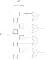
图1是本发明的一种分层全互联结构示意图; Fig. 1 is a schematic diagram of a hierarchical fully interconnected structure of the present invention;
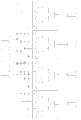
图2是传统全互联结构示意图; Figure 2 is a schematic diagram of a traditional fully interconnected structure;
图3是本发明一种实施例的输入缓存选1到连接开关一电路示意图; Fig. 3 is a schematic diagram of a circuit from input buffer selection 1 to connection switch of an embodiment of the present invention;
图4是本发明一种实施例连接开关一到连接开关二电路示意图; Fig. 4 is a schematic diagram of a connection switch one to a connection switch two circuit diagram of an embodiment of the present invention;
图5是本发明一种实施例案连接开关二到可重构阵列模块的选1电路示意图。 FIG. 5 is a schematic diagram of a select 1
具体实施方式Detailed ways
为使本发明的上述目的、特征和优点能够更加明显易懂,下面结合附图和具体实施方式对本发明作进一步详细的说明。 In order to make the above objects, features and advantages of the present invention more comprehensible, the present invention will be further described in detail below in conjunction with the accompanying drawings and specific embodiments. the
参照图1示出了本发明的一种分层全互联结构示意图。 Referring to FIG. 1 , a schematic diagram of a layered fully interconnected structure of the present invention is shown. the
包括输入缓存阵列模块11,可重构阵列模块14,输出缓存阵列模块17,连接开关一12,连接开关二13,连接开关三15和连接开关四16;可重构阵列模块相邻两列之间全互联;连接开关一12宽度与输入缓存阵列模块11列宽相同,连接开关二13和连接开关三15宽度与可重构阵列模块14列宽相同,连接开关四16与输入缓存阵列模块17列宽相同; Including input cache array module 11,
输入缓存阵列模块11与连接开关一12互联,连接开关一12与连接开关二13全互联,连接开关二13与可重构阵列模块14互联,可重构阵列模块14与连接开关三15互联,连接开关三15与连接开关四16全互联,连接开关四16与输出缓存阵列模块17分互联; The input buffer array module 11 is interconnected with the connection switch one 12, the connection switch one 12 is fully interconnected with the connection switch two 13, the connection switch two 13 is interconnected with the
其中输入缓存阵列模块规模为2m1x2n1,其中2m1为行数,2n1为列数;可重构阵列模块规模为2m2x2n2,其中2m2为行数,2n2为列数;输出缓存阵列模块规模为2m3x2n3,其中2m3为行数,2n3为列数;并和输入缓存规模一致。 The size of the input cache array module is 2m1 x2n1 , where 2m1 is the number of rows and 2n1 is the number of columns; the size of the reconfigurable array module is 2m2 x2n2 , where 2m2 is the number of rows and 2n2 is the number of columns; The size of the output cache array module is 2m3 x2n3 , where 2m3 is the number of rows and 2n3 is the number of columns; and it is consistent with the size of the input cache.
数据由输入缓存阵列模块11输入,然后输入缓存阵列模块11选择一列数据到连接开关一12,连接开关一12将数据输送到连接开关二13,连接开关13选择输入到可重构阵列模块14的一列进行计算单元,数据只可从此列传入相全互联的下一列计算单元进行处理,当可重构阵列模块数据在某一列处理完毕后,处理完数据的那一列计算单元连接到连接开关15,将数据从可重构阵列模块输送到连接开关15,连接开关15将数据输送到连接开关16,连接开关16选择输出缓存的一列连接将数据输出。 The data is input by the input cache array module 11, and then the input cache array module 11 selects a row of data to the connection switch one 12, and the connection switch one 12 transmits the data to the connection switch two 13, and the
其中输入缓存阵列模块的每行按需求与连接开关一全互联;可重构阵列模块的每行按需求与连接开关二全互联;可重构阵列模块的每行按需求与连接开关三全互联;输出缓存的每行按需求与连接开关四全互联; Each row of the input cache array module is fully interconnected with the connection switch 1 according to the requirement; each row of the reconfigurable array module is fully interconnected with the
其中输入缓存阵列模块优选为输入FIFO(First In Out,一种先进先出的数据缓存器),输出缓存阵列模块优选为输出FIFO。 Wherein the input buffer array module is preferably an input FIFO (First In Out, a first-in-first-out data buffer), and the output buffer array module is preferably an output FIFO. the
优选的,可重构阵列模块按列互联形成一维环状结构,例如可重构阵列模块从左至右有4列,那么第1列连接第2列,第2列连接第3列,第3列连接第4列,第4列连接第1列,并且相邻两列之间采取全互联。 Preferably, the reconfigurable array modules are interconnected by column to form a one-dimensional ring structure. For example, the reconfigurable array module has 4 columns from left to right, then the first column is connected to the second column, the second column is connected to the third column, and the second column is connected to the third column. Column 3 is connected to
其中,连接开关一包括与输入缓存阵列模块行的个数相同的子开关,所述的连接开关一的每个子开关连接输入缓存阵列的一行缓存单元。 Wherein, the first connection switch includes the same number of sub-switches as the number of rows of the input buffer array module, and each sub-switch of the first connection switch is connected to a row of buffer units of the input buffer array. the
连接开关二包括与可重构阵列模块行的个数相同的子开关,所述的连接开关二的每个子开关的一端连接可重构阵列模块的一行计算单元。 The
连接开关三包括与可重构阵列模块行的个数相同的子开关,所述的连接开关三的每个子开关的一端连接可重构阵列模块的一行计算单元。 The connection switch three includes the same number of sub-switches as the number of reconfigurable array module rows, and one end of each sub-switch of the connection switch three is connected to a row of computing units of the reconfigurable array module. the
连接开关四包括与输出缓存阵列模块行的个数相同的子开关,所述的连 接开关四的每个子开关的一端连接输出缓存阵列模块的一行缓存单元。
为了充分说明本发明的优点,下面给示出了传统传互联结构作为对比。 In order to fully illustrate the advantages of the present invention, the traditional transmission interconnection structure is shown below as a comparison. the
参照图2,示出了传统全互联结构示意图。 Referring to FIG. 2 , it shows a schematic diagram of a traditional fully interconnected structure. the
传统结构中输入缓存模块21的所有单元与可重构阵列模块22的所有单元之间全互联,可重构阵列模块22的所有单元相互全互联,可重构阵列模块22的所有单元与输出缓存模块23的所有单元之间全互联。比如输入缓存模块为4x2的阵列,可重构阵列模块为4x4的阵列,输出缓存模块为4x2的阵列,那么输入缓存模块的8个单元每个都与与可重构阵列模块的16个单元都相连接,可重构阵列模块的16个单元之间相互连接,输出缓存模块的8个单元每个都与可重构阵列模块的16个单元相连接。其中输入缓存阵列模块规模为2m1x2n1,可重构阵列模块规模为2m2x2n2,输出缓存阵列模块规模为2m3x2n3并和输入缓存规模一致。 In the traditional structure, all units of the input cache module 21 are fully interconnected with all units of the reconfigurable array module 22, all units of the reconfigurable array module 22 are fully interconnected with each other, and all units of the reconfigurable array module 22 are connected to the output cache All units of the module 23 are fully interconnected. For example, the input cache module is a 4x2 array, the reconfigurable array module is a 4x4 array, and the output cache module is a 4x2 array, then each of the 8 units of the input cache module is connected to the 16 units of the reconfigurable array module The 16 units of the reconfigurable array module are connected to each other, and each of the 8 units of the output buffer module is connected to the 16 units of the reconfigurable array module. The size of the input cache array module is 2m1 x2n1 , the size of the reconfigurable array module is 2m2 x2n2 , and the size of the output cache array module is 2m3 x2n3 which is consistent with the size of the input cache.
在传统的全互联结构中,可重构阵列模块为了保证足够的灵活性,需要采用全互联的策略。如上所述,互联的位置分成三个部分: In the traditional fully interconnected structure, in order to ensure sufficient flexibility, the reconfigurable array module needs to adopt a fully interconnected strategy. As mentioned above, interconnected locations are divided into three parts:
1)输入端到计算单元之间的互联 1) The interconnection between the input terminal and the computing unit
2)计算单元之间的互联 2) Interconnection between computing units
3)计算单元到输出端之间的互联 3) The interconnection between the computing unit and the output terminal
图中给出的数种数据互联方式均为示例。 The several data interconnection methods shown in the figure are examples. the
图中输入缓存的宽度为2m1个数据,一次运算所需的数据深度为2n1行。(由于一个任务图所需的数据可能大于缓存宽度2m1,故存在大于等于1的2n1参数。)(使用2的幂指数表示是为了更好的和硬件实现对应,指数上的数据即为编码地址) In the figure, the width of the input cache is 2m1 data, and the data depth required for one operation is 2n1 lines. (Because the data required by a task map may be greater than the
阵列规模为2m2x2n2,数据沿着2n2的方向流动。(由于计算电路总是带有方向性,故可重构阵列模块总能划归成一维的计算数据流。) The size of the array is 2m2 x2n2 , and the data flows along the direction of 2n2 . (Since computing circuits are always directional, reconfigurable array modules can always be classified as one-dimensional computing data flows.)
同理输出缓存的宽度为2m3x2n3,和输入缓存一致。 Similarly, the width of the output buffer is 2m3 x2n3 , which is consistent with the input buffer.
为了更清楚地说明互联的硬件规模,这里先举一个简单的例子:当两排数据之间采用全互联结构,第一排有2m个数据,是源,第二排有2n个数据,是目标。 In order to illustrate the hardware scale of the interconnection more clearly, here is a simple example: when two rows of data adopt a fully interconnected structure, the first row has 2m data, which is the source, and the second row has 2n data, is the target.
1)先从m个数据中选择1个数据给目标地址1: 1) First select 1 data from the m data to the target address 1:
mux开销:2m-1+2m-2+...+20=2m-1(mux为2选1基本电路单元) Mux overhead: 2m-1 +2m-2 +...+20 = 2m -1 (mux is a 2-to-1 basic circuit unit)
2)再重复上述操作2n-1次,使得2n个目标均获得输入数据: 2) Repeat the above operation 2n -1 times, so that all 2n targets can obtain input data:
按乘法乘法原理得:(2m-1)*2nAccording to the principle of multiplication and multiplication: (2m -1)*2n
所以,图1中三部分的全互联结构硬件结构的开销如下: Therefore, the overhead of the hardware structure of the three-part fully interconnected structure in Figure 1 is as follows:
1)输入端到计算单元之间的互联: 1) The interconnection between the input terminal and the computing unit:
(2m1*2n1-1)*(2m2*2n2) (1.1) (2m1 *2n1 -1)*(2m2 *2n2 ) (1.1)
2)计算单元之间的互联: 2) Interconnection between computing units:
(2m2-1)*2m2*(2n2-1+1)/2*(2n2-1)=(2m2-1)*(2n2-1)*2m2*2n2-1 (1.2) (2m2 -1)*2m2 *(2n2 -1+1)/2*(2n2 -1)=(2m2 -1)*(2n2 -1)*2m2 *2n2 -1 ( 1.2)
3)计算单元到输出端之间的互联: 3) The interconnection between the computing unit and the output terminal:
(2m2*2n2-1)*(2m3*2n3) (1.3) (2m2 *2n2 -1)*(2m3 *2n3 ) (1.3)
假定m和n等比例增加,硬件规模和2m*2n成正比。 Assuming that m and n increase proportionally, the hardware scale is proportional to 2m * 2n .
而图1为本发明的一种分层全互联结构示意图。 Fig. 1 is a schematic diagram of a layered fully interconnected structure of the present invention. the
输入缓存从2n1行中选择一列到连接开关一,连接开关一到连接开关二采用全互联,再从2n2行中选择一列连接到连接开关二,如此完成输入缓存到阵列的互联。阵列到输出缓存的连接方式同理。可重构阵列模块只采用行与行之间的全互联。 The input buffer selects a column from the 2n1 rows to connect switch 1, and connects switch 1 to connect
这种互联方式利用算法中数据的局域性,即中相邻的数据大部分情况下在存储器中位置接近。故输入数据可以使用同一行的多个数据,而阵列输入数据位置的调整可以通过阵列中空闲单元进行数据直传,即可以到达所需要的输入位置。当算法映射至可重构阵列模块的过程中,也应当使得计算路径相对比较均衡,这样整个电路图在循环流水的过程中也能取得较高的效率。这说明行间互联也具备算法映射的合理性。 This interconnection method takes advantage of the locality of the data in the algorithm, that is, the adjacent data in the algorithm are mostly close to each other in the memory. Therefore, the input data can use multiple data in the same row, and the adjustment of the input data position of the array can be directly transmitted through the idle units in the array, that is, the required input position can be reached. When the algorithm is mapped to the reconfigurable array module, the calculation path should also be relatively balanced, so that the entire circuit diagram can also achieve higher efficiency in the process of circulating water. This shows that inter-line interconnection also has the rationality of algorithm mapping. the
这里硬件开销的计算如下: The calculation of the hardware overhead here is as follows:
先选择2n1中的一行2m1个数据,需要(2n1-1)*2m1个mux;再实现2m1到2m2个数据之间的全互联,需要(2m1-1)*2m2个mux;最后实现阵列2n1行中选择一行2m2个数据,需要(2n1-1)*2m2个mux。 First select a row of 2m1 data in 2n1 , which requires (2n1 -1)*2m1 muxes; then realize the full interconnection between 2m1 and 2m2 data, which requires (2m1 -1)*2m2 Muxes; Finally, to select a row of 2m2 data in 2n1 rows of the array, (2n1 -1)*2m2 muxes are needed.
故,图2三部分互联结构的硬件开销如下: Therefore, the hardware overhead of the three-part interconnection structure in Figure 2 is as follows:
1)输入端到计算单元之间的互联: 1) The interconnection between the input terminal and the computing unit:
(2n1-1)*2m1+(2m1-1)*2m2+(2n2-1)*2m2 (2.1) (2n1 -1)*2m1 +(2m1 -1)*2m2 +(2n2 -1)*2m2 (2.1)
2)计算单元之间的互联: 2) Interconnection between computing units:
(2m2-1)*2m2*(2n2-1) (2.2) (2m2 -1)*2m2 *(2n2 -1) (2.2)
3)计算单元到输出端之间的互联: 3) The interconnection between the computing unit and the output terminal:
(2n2-1)*2m2+(2m2-1)*2m3+(2n3-1)*2m3 (2.3) (2n2 -1)*2m2 +(2m2 -1)*2m3 +(2n3 -1)*2m3 (2.3)
比较本发明和传统方案中输入互联的部分,
比较本发明和传统方案中阵列互联的部分, 当阵列的行数为16(即n2=4)时,本专利方案的硬件开销约为原来的1/8。 Comparing the part of array interconnection in the present invention and the traditional scheme, When the number of rows of the array is 16 (ie n2=4), the hardware overhead of the patent solution is about 1/8 of the original.
对比三个部分硬件开销的优化幅度如下: Comparing the optimization range of the hardware overhead of the three parts is as follows:
1)输入端到计算单元之间的互联: 1) The interconnection between the input terminal and the computing unit:
2)计算单元之间的互联: 2) Interconnection between computing units:
2n2-1 (3.2) 2n2-1 (3.2)
3)计算单元到输出端之间的互联: 3) The interconnection between the computing unit and the output terminal:
由于每个mux均需要进行配置,故在配置点的数量上,和硬件开销类似,也优化了同等幅度。配置信息量的计算略有不同。原方案中假定所有的配置信息均集中在计算单元上,则输入部分需要(m1+n1)*2m2*2n2;输出部分需要(m3+n3)*2m2*2n2;计算单元之间互联需要(m2+n2)*2m2*2n2。而本专利方案所需配置信息,输入部分需要n1*2n2+m1*2m2;输出部分需要n3*2n2+m3*2m2;计算单元之间互联需要m2*2m2*2n2。 Since each mux needs to be configured, the number of configuration points is similar to the hardware overhead, and the same level of optimization is also optimized. The calculation of configuration information volume is slightly different. In the original scheme, it is assumed that all configuration information is concentrated on the computing unit, then the input part needs (m1+n1)*2m2 *2n2 ; the output part needs (m3+n3)*2m2 *2n2 ; between the computing units The interconnection requires (m2+n2)*2m2 *2n2 . The configuration information required by this patent solution requires n1*2n2 + m1*2m2 for the input part; n3*2n2 + m3*2m2 for the output part; m2*2m2 *2n2 for the interconnection between computing units.
对比三个部分配置信息量的优化幅度如下: Comparing the optimization range of the configuration information of the three parts is as follows:
1)输入端互联配置信息: 1) Input interconnection configuration information:
2)计算单元互联配置信息: 2) Computing unit interconnection configuration information:
3)输出端互联配置信息: 3) Output interconnection configuration information:
当阵列规模为16x16时(即m2=n2=4),输入端的配置信息为原来的1/16;计算单元互联配置信息减少为原来的1/2,输入端的配置信息减少为原来的1/16。 When the array size is 16x16 (that is, m2=n2=4), the configuration information of the input terminal is 1/16 of the original; the interconnection configuration information of the computing unit is reduced to 1/2 of the original, and the configuration information of the input terminal is reduced to 1/16 of the original . the
作为对比,下面为传统全互联结构面积效率实例: For comparison, the following is an example of the area efficiency of the traditional fully interconnected structure:
输入缓存宽度16,单个循环可配置深度8,阵列规模8x8,输出缓存宽度16,单次循环可配置深度8。数据粒度为16比特。采用tsmc65lp工艺,经统计各部分面积比重如下: The input buffer width is 16, the depth of a single cycle can be configured to be 8, the array size is 8x8, the output buffer width is 16, and the depth of a single cycle can be configured to be 8. The data granularity is 16 bits. Using tsmc65lp technology, the area proportion of each part is as follows:
由于阵列具有可扩展的特性,则当阵列规模为16x16、32x32时,推演各部分面积比重如下(输入输出结构同比增大): Due to the scalable nature of the array, when the array size is 16x16 and 32x32, the area ratio of each part is deduced as follows (the input and output structures increase year-on-year):
阵列的长宽各扩展4倍以上,可重构处理器95%以上的面积就被互联消耗掉了。互联面积从原来8x8时是计算单元面积开销的约2倍,到32x32时已经是30倍以上。此时只有小于5%的面积用于真正的计算,大于95%的面积用于数据传递,这样的面积效率显失公平,是不可接受的。 The length and width of the array are expanded by more than 4 times, and more than 95% of the area of the reconfigurable processor is consumed by the interconnection. The interconnection area is about 2 times that of the computing unit area when it was originally 8x8, and it is more than 30 times when it is 32x32. At this time, only less than 5% of the area is used for real calculation, and more than 95% of the area is used for data transmission. Such an area efficiency is unfair and unacceptable. the
下面为本发明面积效率实例: Below is the area efficiency example of the present invention:
当采用本发明所述的分层全互联结构时,面积比重变化为: When adopting the layered fully interconnected structure described in the present invention, the area proportion changes as:
当阵列规模扩展时: When the array scales up:

阵列的长宽各扩展4倍时,可重构处理器1/3左右的面积用于互联,1/3用于计算,1/3用于存储,保持了一个合理的面积效率。输入输出部分的互联开销和计算单元的增加一致,主要在于阵列宽度的增加,导致阵列内部的互联以大于一次方的关系增加。一般情况下,在阵列规模更大的情况下,整个可重构处理器的面积效率还是可以保持在 When the length and width of the array are expanded by 4 times, about 1/3 of the area of the reconfigurable processor is used for interconnection, 1/3 is used for computing, and 1/3 is used for storage, maintaining a reasonable area efficiency. The interconnection overhead of the input and output part is consistent with the increase of the computing unit, mainly due to the increase of the array width, which leads to the increase of the interconnection within the array with a relationship greater than one power. In general, the area efficiency of the entire reconfigurable processor can still be maintained at

相对传统全互联结构,这是十分高效的面积使用方式。 Compared with the traditional fully interconnected structure, this is a very efficient way to use the area. the
故,不论从面积使用效率,还是配置信息量的压缩(服务于动态重构),上述分层全互联结构均为一种非常优秀的动态可重构处理器互联结构。 Therefore, regardless of the area utilization efficiency or the compression of configuration information (serving for dynamic reconfiguration), the above-mentioned layered full interconnection structure is a very excellent dynamic reconfigurable processor interconnection structure. the
图3示出了当输入FIFO宽度为4(也即行数为4),单次循环数据深度为2(也即为列数为2),可重构阵列模块大小为4x4,输出FIFO宽度为4(也即行数为4),单次循环数据深度为2(也即为列数为2)时,输入FIFO到连接开关一的电路示意图。p1为输入FIFO的宽度(也即行数),p2为输入FIFO的深度(即列数)。 Figure 3 shows that when the input FIFO width is 4 (that is, the number of rows is 4), the data depth of a single cycle is 2 (that is, the number of columns is 2), the reconfigurable array module size is 4x4, and the output FIFO width is 4 (that is, the number of rows is 4), and when the data depth of a single cycle is 2 (that is, the number of columns is 2), the schematic diagram of the circuit from the input FIFO to the connection switch 1. p1 is the width of the input FIFO (that is, the number of rows), and p2 is the depth of the input FIFO (that is, the number of columns). the
图4示出了当输入FIFO宽度为4(也即行数为4),单次循环数据深度为2(也即为列数为2),可重构阵列模块大小为4x4,输出FIFO宽度为4(也即行数为4),单次循环数据深度为2(也即为列数为2)时,连接开关一到连接开关二的电路示意图 Figure 4 shows that when the input FIFO width is 4 (that is, the number of rows is 4), the data depth of a single cycle is 2 (that is, the number of columns is 2), the reconfigurable array module size is 4x4, and the output FIFO width is 4 (That is, the number of rows is 4), when the data depth of a single cycle is 2 (that is, the number of columns is 2), the circuit diagram of the connection switch 1 to the
图5示出了当输入FIFO宽度为4(也即行数为4),单次循环数据深度为2(也即为列数为2),可重构阵列模块大小为4x4,输出FIFO宽度为4(也即行数为4),单次循环数据深度为2(也即为列数为2)时,连接开关二到 可重构阵列模块的电路示意图。q1为行地址0,q2为行地址1。 Figure 5 shows that when the input FIFO width is 4 (that is, the number of rows is 4), the data depth of a single cycle is 2 (that is, the number of columns is 2), the reconfigurable array module size is 4x4, and the output FIFO width is 4 (that is, the number of rows is 4), and when the data depth of a single cycle is 2 (that is, the number of columns is 2), the schematic diagram of the
图中a1开关中,如果选择第一行,则{行地址0,行地址1}=11,选择第二行,则{行地址0,行地址1}=01,选择第三行,则{行地址0,行地址1}=10,选择第四行,则{行地址0,行地址1}=00。 In the a1 switch in the figure, if the first row is selected, {row address 0, row address 1}=11, if the second row is selected, {row address 0, row address 1}=01, and the third row is selected, then { Row address 0, row address 1}=10, select the fourth row, then {row address 0, row address 1}=00. the
当{行地址0,行地址1}=11时,开关s1打开,开关s5打开,选通第一行,开关s2关闭,开关s6打开,不选通第二行,开关s3打开,开关s7关闭,不选通第三行,开关s4关闭,开关s8关闭,不选通第四行。 When {row address 0, row address 1}=11, the switch s1 is turned on, the switch s5 is turned on, the first row is selected, the switch s2 is turned off, the switch s6 is turned on, the second row is not selected, the switch s3 is turned on, and the switch s7 is turned off , the third line is not selected, the switch s4 is closed, the switch s8 is closed, and the fourth line is not selected. the
开关电路有很多种实现形式,比如晶体管就是一个开关。 There are many implementation forms of switching circuits, for example, a transistor is a switch. the
以上对本发明所提供的一种全互联路由结构动态可重构处理器进行了详细介绍,本文中应用了具体个例对本发明的原理及实施方式进行了阐述,以上实施例的说明只是用于帮助理解本发明的方法及其核心思想;同时,对于本领域的一般技术人员,依据本发明的思想,在具体实施方式及应用范围上均会有改变之处,综上所述,本说明书内容不应理解为对本发明的限制。 A dynamic reconfigurable processor with fully interconnected routing structure provided by the present invention has been introduced in detail above. In this paper, specific examples are used to illustrate the principle and implementation of the present invention. The description of the above embodiments is only for helping Understand the method of the present invention and its core idea; at the same time, for those of ordinary skill in the art, according to the idea of the present invention, there will be changes in the specific implementation and scope of application. In summary, the content of this specification is not It should be understood as a limitation of the present invention. the
Claims (3)
Priority Applications (1)
| Application Number | Priority Date | Filing Date | Title |
|---|---|---|---|
| CN 201110152238CN102214158B (en) | 2011-06-08 | 2011-06-08 | A Dynamically Reconfigurable Processor with Fully Interconnected Routing Structure |
Applications Claiming Priority (1)
| Application Number | Priority Date | Filing Date | Title |
|---|---|---|---|
| CN 201110152238CN102214158B (en) | 2011-06-08 | 2011-06-08 | A Dynamically Reconfigurable Processor with Fully Interconnected Routing Structure |
Publications (2)
| Publication Number | Publication Date |
|---|---|
| CN102214158A CN102214158A (en) | 2011-10-12 |
| CN102214158Btrue CN102214158B (en) | 2013-05-22 |
Family
ID=44745473
Family Applications (1)
| Application Number | Title | Priority Date | Filing Date |
|---|---|---|---|
| CN 201110152238ActiveCN102214158B (en) | 2011-06-08 | 2011-06-08 | A Dynamically Reconfigurable Processor with Fully Interconnected Routing Structure |
Country Status (1)
| Country | Link |
|---|---|
| CN (1) | CN102214158B (en) |
Families Citing this family (8)
| Publication number | Priority date | Publication date | Assignee | Title |
|---|---|---|---|---|
| CN102541809B (en)* | 2011-12-08 | 2015-03-04 | 清华大学 | Dynamic reconfigurable processor |
| KR101912427B1 (en)* | 2011-12-12 | 2018-10-29 | 삼성전자주식회사 | Reconfigurable processor and mini-core of reconfigurable processor |
| CN102650980B (en)* | 2012-04-09 | 2014-07-23 | 清华大学 | Method and device for generating configuration information with multi-core dynamic reconfigurable processor |
| US9479456B2 (en)* | 2012-11-02 | 2016-10-25 | Altera Corporation | Programmable logic device with integrated network-on-chip |
| US9210486B2 (en) | 2013-03-01 | 2015-12-08 | Qualcomm Incorporated | Switching fabric for embedded reconfigurable computing |
| CN108153549B (en) | 2017-12-13 | 2020-08-28 | 京微齐力(北京)科技有限公司 | FPGA chip of distributed multi-functional-layer structure |
| CN109445752B (en)* | 2018-10-10 | 2019-10-15 | 西安交通大学 | A parallel computing system |
| CN112486905B (en)* | 2020-12-18 | 2024-06-25 | 清华大学 | Reconfigurable Heterogeneous PEA Interconnection Method |
Family Cites Families (3)
| Publication number | Priority date | Publication date | Assignee | Title |
|---|---|---|---|---|
| US6920545B2 (en)* | 2002-01-17 | 2005-07-19 | Raytheon Company | Reconfigurable processor with alternately interconnected arithmetic and memory nodes of crossbar switched cluster |
| CN1564125A (en)* | 2004-04-09 | 2005-01-12 | 哈尔滨工业大学 | Array type reconstructural DSP engine chip structure based on CORDIC unit |
| JP2007141132A (en)* | 2005-11-22 | 2007-06-07 | Renesas Technology Corp | Dynamically-reconfigurable processor and processor control program which controls the same |
- 2011
- 2011-06-08CNCN 201110152238patent/CN102214158B/enactiveActive
Also Published As
| Publication number | Publication date |
|---|---|
| CN102214158A (en) | 2011-10-12 |
Similar Documents
| Publication | Publication Date | Title |
|---|---|---|
| CN102214158B (en) | A Dynamically Reconfigurable Processor with Fully Interconnected Routing Structure | |
| US8478964B2 (en) | Stall propagation in a processing system with interspersed processors and communicaton elements | |
| US20160344629A1 (en) | Directional two-dimensional router and interconnection network for field programmable gate arrays, and other circuits and applications of the router and network | |
| EP3144820B1 (en) | Inter-cluster data communication network for a dynamic shared communication platform | |
| WO2016191304A1 (en) | Directional two-dimensional router and interconnection network for field programmable gate arrays, and other circuits, and applications of the router and network | |
| Feng et al. | A scalable methodology for designing efficient interconnection network of chiplets | |
| JP2018073413A (en) | DRAM-based stochastic computing system | |
| CN102799563A (en) | Reconfigurable computing array and construction method | |
| CN111630487A (en) | Centralized-distributed hybrid organization of shared memory for neural network processing | |
| Ahn et al. | Network within a network approach to create a scalable high-radix router microarchitecture | |
| CN101620587A (en) | Flexible reconfigurable task processing unit structure | |
| CN104035896B (en) | Off-chip accelerator applicable to fusion memory of 2.5D (2.5 dimensional) multi-core system | |
| Xue et al. | 3D floorplanning of low-power and area-efficient Network-on-Chip architecture | |
| Guo et al. | Network-on-Chip (NoC) applications for iot-enabled chip systems: latest designs and modern applications | |
| CN102253920B (en) | Fully-interconnected route structure dynamically-reconfigurable data processing method and processor | |
| CN107807901A (en) | A kind of expansible restructural polycaryon processor connection method | |
| Paul et al. | Energy-efficient hardware acceleration through computing in the memory | |
| Asad et al. | Godiva: green on-chip interconnection for DNNs | |
| CN103914429A (en) | Multi-mode data transmission interconnection device for coarseness dynamic reconfigurable array | |
| CN203982379U (en) | For the multimode data transmission connectors of coarseness dynamic reconfigurable array | |
| CN112486905A (en) | Reconfigurable isomerization PEA interconnection method | |
| CN118093504B (en) | A storage and computing FPGA based on NoC efficient interconnection | |
| Mnejja et al. | Implementing on-chip wireless communication in multi-stage interconnection NoCs | |
| Luo et al. | Hybrid circuit-switched network for on-chip communication in large-scale chip-multiprocessors | |
| Mulajkar et al. | ANALYSIS OF IMPROVED EZ-PASS ROUTER DESIGN AND ITS FPGA IMPLEMENTATION |
Legal Events
| Date | Code | Title | Description |
|---|---|---|---|
| C06 | Publication | ||
| PB01 | Publication | ||
| C10 | Entry into substantive examination | ||
| SE01 | Entry into force of request for substantive examination | ||
| C14 | Grant of patent or utility model | ||
| GR01 | Patent grant | ||
| ASS | Succession or assignment of patent right | Owner name:WUXI APPLICATION TECHNOLOGY RESEARCH INSTITUTE OF Free format text:FORMER OWNER: TSINGHUA UNIVERSITY Effective date:20141219 | |
| C41 | Transfer of patent application or patent right or utility model | ||
| COR | Change of bibliographic data | Free format text:CORRECT: ADDRESS; FROM: 100084 HAIDIAN, BEIJING TO: 214072 WUXI, JIANGSU PROVINCE | |
| TR01 | Transfer of patent right | Effective date of registration:20141219 Address after:214072, A3 building, No. 777 West Building Road, Binhu District, Jiangsu, Wuxi 4, China Patentee after:Wuxi Research Institute of Applied Technologies Tsinghua University Address before:100084 Tsinghua Yuan, Beijing, Haidian District Patentee before:Tsinghua University | |
| ASS | Succession or assignment of patent right | Owner name:SHENZHEN PANGO MICROSYSTEMS CO., LTD. Free format text:FORMER OWNER: WUXI APPLICATION TECHNOLOGY RESEARCH INSTITUTE OF TSINGHUA UNIVERSITY Effective date:20150611 | |
| C41 | Transfer of patent application or patent right or utility model | ||
| TR01 | Transfer of patent right | Effective date of registration:20150611 Address after:518057 Guangdong city of Shenzhen province Nanshan District high tech Industrial Park Road eight South South technology Howare Technology Building 16 Patentee after:Shenzhen Tongchuang Guoxin Electronics Co.,Ltd. Address before:214072, A3 building, No. 777 West Building Road, Binhu District, Jiangsu, Wuxi 4, China Patentee before:Wuxi Research Institute of Applied Technologies Tsinghua University | |
| C56 | Change in the name or address of the patentee | ||
| CP01 | Change in the name or title of a patent holder | Address after:518057 Guangdong city of Shenzhen province Nanshan District high tech Industrial Park Road eight South South technology Howare Technology Building 16 Patentee after:SHENZHEN PANGO MICROSYSTEMS Co.,Ltd. Address before:518057 Guangdong city of Shenzhen province Nanshan District high tech Industrial Park Road eight South South technology Howare Technology Building 16 Patentee before:Shenzhen Tongchuang Guoxin Electronics Co.,Ltd. | |
| CP03 | Change of name, title or address | ||
| CP03 | Change of name, title or address | Address after:518000 Guowei R & D building 401, No.015, Gaoxin South 1st Road, high tech Zone community, Yuehai street, Nanshan District, Shenzhen City, Guangdong Province Patentee after:Shenzhen Ziguang Tongchuang Electronics Co.,Ltd. Country or region after:China Address before:16th Floor, Haowei Technology Building, Science and Technology South Eighth Road, Nanshan District, Shenzhen, Guangdong Province, China Patentee before:SHENZHEN PANGO MICROSYSTEMS Co.,Ltd. Country or region before:China |