CN102201385B - Quad flat no-lead semiconductor package and manufacturing method thereof - Google Patents
Quad flat no-lead semiconductor package and manufacturing method thereofDownload PDFInfo
- Publication number
- CN102201385B CN102201385BCN2011101081892ACN201110108189ACN102201385BCN 102201385 BCN102201385 BCN 102201385BCN 2011101081892 ACN2011101081892 ACN 2011101081892ACN 201110108189 ACN201110108189 ACN 201110108189ACN 102201385 BCN102201385 BCN 102201385B
- Authority
- CN
- China
- Prior art keywords
- lead
- bonding
- leads
- external terminal
- semiconductor package
- Prior art date
- Legal status (The legal status is an assumption and is not a legal conclusion. Google has not performed a legal analysis and makes no representation as to the accuracy of the status listed.)
- Expired - Fee Related
Links
Images


Classifications
- H—ELECTRICITY
- H01—ELECTRIC ELEMENTS
- H01L—SEMICONDUCTOR DEVICES NOT COVERED BY CLASS H10
- H01L23/00—Details of semiconductor or other solid state devices
- H01L23/28—Encapsulations, e.g. encapsulating layers, coatings, e.g. for protection
- H01L23/31—Encapsulations, e.g. encapsulating layers, coatings, e.g. for protection characterised by the arrangement or shape
- H01L23/3107—Encapsulations, e.g. encapsulating layers, coatings, e.g. for protection characterised by the arrangement or shape the device being completely enclosed
- H—ELECTRICITY
- H01—ELECTRIC ELEMENTS
- H01L—SEMICONDUCTOR DEVICES NOT COVERED BY CLASS H10
- H01L21/00—Processes or apparatus adapted for the manufacture or treatment of semiconductor or solid state devices or of parts thereof
- H01L21/02—Manufacture or treatment of semiconductor devices or of parts thereof
- H01L21/04—Manufacture or treatment of semiconductor devices or of parts thereof the devices having potential barriers, e.g. a PN junction, depletion layer or carrier concentration layer
- H01L21/48—Manufacture or treatment of parts, e.g. containers, prior to assembly of the devices, using processes not provided for in a single one of the groups H01L21/18 - H01L21/326 or H10D48/04 - H10D48/07
- H01L21/4814—Conductive parts
- H01L21/4821—Flat leads, e.g. lead frames with or without insulating supports
- H01L21/4828—Etching
- H01L21/4832—Etching a temporary substrate after encapsulation process to form leads
- H—ELECTRICITY
- H01—ELECTRIC ELEMENTS
- H01L—SEMICONDUCTOR DEVICES NOT COVERED BY CLASS H10
- H01L23/00—Details of semiconductor or other solid state devices
- H01L23/48—Arrangements for conducting electric current to or from the solid state body in operation, e.g. leads, terminal arrangements ; Selection of materials therefor
- H01L23/488—Arrangements for conducting electric current to or from the solid state body in operation, e.g. leads, terminal arrangements ; Selection of materials therefor consisting of soldered or bonded constructions
- H01L23/495—Lead-frames or other flat leads
- H01L23/49503—Lead-frames or other flat leads characterised by the die pad
- H—ELECTRICITY
- H01—ELECTRIC ELEMENTS
- H01L—SEMICONDUCTOR DEVICES NOT COVERED BY CLASS H10
- H01L23/00—Details of semiconductor or other solid state devices
- H01L23/48—Arrangements for conducting electric current to or from the solid state body in operation, e.g. leads, terminal arrangements ; Selection of materials therefor
- H01L23/488—Arrangements for conducting electric current to or from the solid state body in operation, e.g. leads, terminal arrangements ; Selection of materials therefor consisting of soldered or bonded constructions
- H01L23/495—Lead-frames or other flat leads
- H01L23/49541—Geometry of the lead-frame
- H01L23/49548—Cross section geometry
- H—ELECTRICITY
- H01—ELECTRIC ELEMENTS
- H01L—SEMICONDUCTOR DEVICES NOT COVERED BY CLASS H10
- H01L23/00—Details of semiconductor or other solid state devices
- H01L23/48—Arrangements for conducting electric current to or from the solid state body in operation, e.g. leads, terminal arrangements ; Selection of materials therefor
- H01L23/488—Arrangements for conducting electric current to or from the solid state body in operation, e.g. leads, terminal arrangements ; Selection of materials therefor consisting of soldered or bonded constructions
- H01L23/495—Lead-frames or other flat leads
- H01L23/49579—Lead-frames or other flat leads characterised by the materials of the lead frames or layers thereon
- H01L23/49586—Insulating layers on lead frames
- H—ELECTRICITY
- H01—ELECTRIC ELEMENTS
- H01L—SEMICONDUCTOR DEVICES NOT COVERED BY CLASS H10
- H01L24/00—Arrangements for connecting or disconnecting semiconductor or solid-state bodies; Methods or apparatus related thereto
- H01L24/01—Means for bonding being attached to, or being formed on, the surface to be connected, e.g. chip-to-package, die-attach, "first-level" interconnects; Manufacturing methods related thereto
- H01L24/42—Wire connectors; Manufacturing methods related thereto
- H01L24/47—Structure, shape, material or disposition of the wire connectors after the connecting process
- H01L24/49—Structure, shape, material or disposition of the wire connectors after the connecting process of a plurality of wire connectors
- H—ELECTRICITY
- H01—ELECTRIC ELEMENTS
- H01L—SEMICONDUCTOR DEVICES NOT COVERED BY CLASS H10
- H01L2224/00—Indexing scheme for arrangements for connecting or disconnecting semiconductor or solid-state bodies and methods related thereto as covered by H01L24/00
- H01L2224/01—Means for bonding being attached to, or being formed on, the surface to be connected, e.g. chip-to-package, die-attach, "first-level" interconnects; Manufacturing methods related thereto
- H01L2224/02—Bonding areas; Manufacturing methods related thereto
- H01L2224/04—Structure, shape, material or disposition of the bonding areas prior to the connecting process
- H01L2224/05—Structure, shape, material or disposition of the bonding areas prior to the connecting process of an individual bonding area
- H01L2224/0554—External layer
- H01L2224/0555—Shape
- H01L2224/05552—Shape in top view
- H01L2224/05554—Shape in top view being square
- H—ELECTRICITY
- H01—ELECTRIC ELEMENTS
- H01L—SEMICONDUCTOR DEVICES NOT COVERED BY CLASS H10
- H01L2224/00—Indexing scheme for arrangements for connecting or disconnecting semiconductor or solid-state bodies and methods related thereto as covered by H01L24/00
- H01L2224/01—Means for bonding being attached to, or being formed on, the surface to be connected, e.g. chip-to-package, die-attach, "first-level" interconnects; Manufacturing methods related thereto
- H01L2224/26—Layer connectors, e.g. plate connectors, solder or adhesive layers; Manufacturing methods related thereto
- H01L2224/31—Structure, shape, material or disposition of the layer connectors after the connecting process
- H01L2224/32—Structure, shape, material or disposition of the layer connectors after the connecting process of an individual layer connector
- H01L2224/321—Disposition
- H01L2224/32151—Disposition the layer connector connecting between a semiconductor or solid-state body and an item not being a semiconductor or solid-state body, e.g. chip-to-substrate, chip-to-passive
- H01L2224/32221—Disposition the layer connector connecting between a semiconductor or solid-state body and an item not being a semiconductor or solid-state body, e.g. chip-to-substrate, chip-to-passive the body and the item being stacked
- H01L2224/32245—Disposition the layer connector connecting between a semiconductor or solid-state body and an item not being a semiconductor or solid-state body, e.g. chip-to-substrate, chip-to-passive the body and the item being stacked the item being metallic
- H01L2224/32257—Disposition the layer connector connecting between a semiconductor or solid-state body and an item not being a semiconductor or solid-state body, e.g. chip-to-substrate, chip-to-passive the body and the item being stacked the item being metallic the layer connector connecting to a bonding area disposed in a recess of the surface of the item
- H—ELECTRICITY
- H01—ELECTRIC ELEMENTS
- H01L—SEMICONDUCTOR DEVICES NOT COVERED BY CLASS H10
- H01L2224/00—Indexing scheme for arrangements for connecting or disconnecting semiconductor or solid-state bodies and methods related thereto as covered by H01L24/00
- H01L2224/01—Means for bonding being attached to, or being formed on, the surface to be connected, e.g. chip-to-package, die-attach, "first-level" interconnects; Manufacturing methods related thereto
- H01L2224/42—Wire connectors; Manufacturing methods related thereto
- H01L2224/44—Structure, shape, material or disposition of the wire connectors prior to the connecting process
- H01L2224/45—Structure, shape, material or disposition of the wire connectors prior to the connecting process of an individual wire connector
- H01L2224/45001—Core members of the connector
- H01L2224/45099—Material
- H01L2224/451—Material with a principal constituent of the material being a metal or a metalloid, e.g. boron (B), silicon (Si), germanium (Ge), arsenic (As), antimony (Sb), tellurium (Te) and polonium (Po), and alloys thereof
- H01L2224/45138—Material with a principal constituent of the material being a metal or a metalloid, e.g. boron (B), silicon (Si), germanium (Ge), arsenic (As), antimony (Sb), tellurium (Te) and polonium (Po), and alloys thereof the principal constituent melting at a temperature of greater than or equal to 950°C and less than 1550°C
- H01L2224/45144—Gold (Au) as principal constituent
- H—ELECTRICITY
- H01—ELECTRIC ELEMENTS
- H01L—SEMICONDUCTOR DEVICES NOT COVERED BY CLASS H10
- H01L2224/00—Indexing scheme for arrangements for connecting or disconnecting semiconductor or solid-state bodies and methods related thereto as covered by H01L24/00
- H01L2224/01—Means for bonding being attached to, or being formed on, the surface to be connected, e.g. chip-to-package, die-attach, "first-level" interconnects; Manufacturing methods related thereto
- H01L2224/42—Wire connectors; Manufacturing methods related thereto
- H01L2224/47—Structure, shape, material or disposition of the wire connectors after the connecting process
- H01L2224/48—Structure, shape, material or disposition of the wire connectors after the connecting process of an individual wire connector
- H01L2224/4805—Shape
- H01L2224/4809—Loop shape
- H01L2224/48091—Arched
- H—ELECTRICITY
- H01—ELECTRIC ELEMENTS
- H01L—SEMICONDUCTOR DEVICES NOT COVERED BY CLASS H10
- H01L2224/00—Indexing scheme for arrangements for connecting or disconnecting semiconductor or solid-state bodies and methods related thereto as covered by H01L24/00
- H01L2224/01—Means for bonding being attached to, or being formed on, the surface to be connected, e.g. chip-to-package, die-attach, "first-level" interconnects; Manufacturing methods related thereto
- H01L2224/42—Wire connectors; Manufacturing methods related thereto
- H01L2224/47—Structure, shape, material or disposition of the wire connectors after the connecting process
- H01L2224/48—Structure, shape, material or disposition of the wire connectors after the connecting process of an individual wire connector
- H01L2224/481—Disposition
- H01L2224/48151—Connecting between a semiconductor or solid-state body and an item not being a semiconductor or solid-state body, e.g. chip-to-substrate, chip-to-passive
- H01L2224/48221—Connecting between a semiconductor or solid-state body and an item not being a semiconductor or solid-state body, e.g. chip-to-substrate, chip-to-passive the body and the item being stacked
- H01L2224/48245—Connecting between a semiconductor or solid-state body and an item not being a semiconductor or solid-state body, e.g. chip-to-substrate, chip-to-passive the body and the item being stacked the item being metallic
- H01L2224/48247—Connecting between a semiconductor or solid-state body and an item not being a semiconductor or solid-state body, e.g. chip-to-substrate, chip-to-passive the body and the item being stacked the item being metallic connecting the wire to a bond pad of the item
- H—ELECTRICITY
- H01—ELECTRIC ELEMENTS
- H01L—SEMICONDUCTOR DEVICES NOT COVERED BY CLASS H10
- H01L2224/00—Indexing scheme for arrangements for connecting or disconnecting semiconductor or solid-state bodies and methods related thereto as covered by H01L24/00
- H01L2224/01—Means for bonding being attached to, or being formed on, the surface to be connected, e.g. chip-to-package, die-attach, "first-level" interconnects; Manufacturing methods related thereto
- H01L2224/42—Wire connectors; Manufacturing methods related thereto
- H01L2224/47—Structure, shape, material or disposition of the wire connectors after the connecting process
- H01L2224/48—Structure, shape, material or disposition of the wire connectors after the connecting process of an individual wire connector
- H01L2224/481—Disposition
- H01L2224/48151—Connecting between a semiconductor or solid-state body and an item not being a semiconductor or solid-state body, e.g. chip-to-substrate, chip-to-passive
- H01L2224/48221—Connecting between a semiconductor or solid-state body and an item not being a semiconductor or solid-state body, e.g. chip-to-substrate, chip-to-passive the body and the item being stacked
- H01L2224/48245—Connecting between a semiconductor or solid-state body and an item not being a semiconductor or solid-state body, e.g. chip-to-substrate, chip-to-passive the body and the item being stacked the item being metallic
- H01L2224/48253—Connecting between a semiconductor or solid-state body and an item not being a semiconductor or solid-state body, e.g. chip-to-substrate, chip-to-passive the body and the item being stacked the item being metallic connecting the wire to a potential ring of the item
- H—ELECTRICITY
- H01—ELECTRIC ELEMENTS
- H01L—SEMICONDUCTOR DEVICES NOT COVERED BY CLASS H10
- H01L2224/00—Indexing scheme for arrangements for connecting or disconnecting semiconductor or solid-state bodies and methods related thereto as covered by H01L24/00
- H01L2224/01—Means for bonding being attached to, or being formed on, the surface to be connected, e.g. chip-to-package, die-attach, "first-level" interconnects; Manufacturing methods related thereto
- H01L2224/42—Wire connectors; Manufacturing methods related thereto
- H01L2224/47—Structure, shape, material or disposition of the wire connectors after the connecting process
- H01L2224/49—Structure, shape, material or disposition of the wire connectors after the connecting process of a plurality of wire connectors
- H01L2224/491—Disposition
- H01L2224/4911—Disposition the connectors being bonded to at least one common bonding area, e.g. daisy chain
- H—ELECTRICITY
- H01—ELECTRIC ELEMENTS
- H01L—SEMICONDUCTOR DEVICES NOT COVERED BY CLASS H10
- H01L2224/00—Indexing scheme for arrangements for connecting or disconnecting semiconductor or solid-state bodies and methods related thereto as covered by H01L24/00
- H01L2224/01—Means for bonding being attached to, or being formed on, the surface to be connected, e.g. chip-to-package, die-attach, "first-level" interconnects; Manufacturing methods related thereto
- H01L2224/42—Wire connectors; Manufacturing methods related thereto
- H01L2224/47—Structure, shape, material or disposition of the wire connectors after the connecting process
- H01L2224/49—Structure, shape, material or disposition of the wire connectors after the connecting process of a plurality of wire connectors
- H01L2224/491—Disposition
- H01L2224/4912—Layout
- H01L2224/49171—Fan-out arrangements
- H—ELECTRICITY
- H01—ELECTRIC ELEMENTS
- H01L—SEMICONDUCTOR DEVICES NOT COVERED BY CLASS H10
- H01L2224/00—Indexing scheme for arrangements for connecting or disconnecting semiconductor or solid-state bodies and methods related thereto as covered by H01L24/00
- H01L2224/01—Means for bonding being attached to, or being formed on, the surface to be connected, e.g. chip-to-package, die-attach, "first-level" interconnects; Manufacturing methods related thereto
- H01L2224/42—Wire connectors; Manufacturing methods related thereto
- H01L2224/47—Structure, shape, material or disposition of the wire connectors after the connecting process
- H01L2224/49—Structure, shape, material or disposition of the wire connectors after the connecting process of a plurality of wire connectors
- H01L2224/491—Disposition
- H01L2224/4912—Layout
- H01L2224/49175—Parallel arrangements
- H—ELECTRICITY
- H01—ELECTRIC ELEMENTS
- H01L—SEMICONDUCTOR DEVICES NOT COVERED BY CLASS H10
- H01L24/00—Arrangements for connecting or disconnecting semiconductor or solid-state bodies; Methods or apparatus related thereto
- H01L24/01—Means for bonding being attached to, or being formed on, the surface to be connected, e.g. chip-to-package, die-attach, "first-level" interconnects; Manufacturing methods related thereto
- H01L24/42—Wire connectors; Manufacturing methods related thereto
- H01L24/44—Structure, shape, material or disposition of the wire connectors prior to the connecting process
- H01L24/45—Structure, shape, material or disposition of the wire connectors prior to the connecting process of an individual wire connector
- H—ELECTRICITY
- H01—ELECTRIC ELEMENTS
- H01L—SEMICONDUCTOR DEVICES NOT COVERED BY CLASS H10
- H01L24/00—Arrangements for connecting or disconnecting semiconductor or solid-state bodies; Methods or apparatus related thereto
- H01L24/01—Means for bonding being attached to, or being formed on, the surface to be connected, e.g. chip-to-package, die-attach, "first-level" interconnects; Manufacturing methods related thereto
- H01L24/42—Wire connectors; Manufacturing methods related thereto
- H01L24/47—Structure, shape, material or disposition of the wire connectors after the connecting process
- H01L24/48—Structure, shape, material or disposition of the wire connectors after the connecting process of an individual wire connector
- H—ELECTRICITY
- H01—ELECTRIC ELEMENTS
- H01L—SEMICONDUCTOR DEVICES NOT COVERED BY CLASS H10
- H01L2924/00—Indexing scheme for arrangements or methods for connecting or disconnecting semiconductor or solid-state bodies as covered by H01L24/00
- H01L2924/01—Chemical elements
- H01L2924/01005—Boron [B]
- H—ELECTRICITY
- H01—ELECTRIC ELEMENTS
- H01L—SEMICONDUCTOR DEVICES NOT COVERED BY CLASS H10
- H01L2924/00—Indexing scheme for arrangements or methods for connecting or disconnecting semiconductor or solid-state bodies as covered by H01L24/00
- H01L2924/01—Chemical elements
- H01L2924/01006—Carbon [C]
- H—ELECTRICITY
- H01—ELECTRIC ELEMENTS
- H01L—SEMICONDUCTOR DEVICES NOT COVERED BY CLASS H10
- H01L2924/00—Indexing scheme for arrangements or methods for connecting or disconnecting semiconductor or solid-state bodies as covered by H01L24/00
- H01L2924/01—Chemical elements
- H01L2924/01015—Phosphorus [P]
- H—ELECTRICITY
- H01—ELECTRIC ELEMENTS
- H01L—SEMICONDUCTOR DEVICES NOT COVERED BY CLASS H10
- H01L2924/00—Indexing scheme for arrangements or methods for connecting or disconnecting semiconductor or solid-state bodies as covered by H01L24/00
- H01L2924/01—Chemical elements
- H01L2924/01028—Nickel [Ni]
- H—ELECTRICITY
- H01—ELECTRIC ELEMENTS
- H01L—SEMICONDUCTOR DEVICES NOT COVERED BY CLASS H10
- H01L2924/00—Indexing scheme for arrangements or methods for connecting or disconnecting semiconductor or solid-state bodies as covered by H01L24/00
- H01L2924/01—Chemical elements
- H01L2924/01029—Copper [Cu]
- H—ELECTRICITY
- H01—ELECTRIC ELEMENTS
- H01L—SEMICONDUCTOR DEVICES NOT COVERED BY CLASS H10
- H01L2924/00—Indexing scheme for arrangements or methods for connecting or disconnecting semiconductor or solid-state bodies as covered by H01L24/00
- H01L2924/01—Chemical elements
- H01L2924/01033—Arsenic [As]
- H—ELECTRICITY
- H01—ELECTRIC ELEMENTS
- H01L—SEMICONDUCTOR DEVICES NOT COVERED BY CLASS H10
- H01L2924/00—Indexing scheme for arrangements or methods for connecting or disconnecting semiconductor or solid-state bodies as covered by H01L24/00
- H01L2924/01—Chemical elements
- H01L2924/01078—Platinum [Pt]
- H—ELECTRICITY
- H01—ELECTRIC ELEMENTS
- H01L—SEMICONDUCTOR DEVICES NOT COVERED BY CLASS H10
- H01L2924/00—Indexing scheme for arrangements or methods for connecting or disconnecting semiconductor or solid-state bodies as covered by H01L24/00
- H01L2924/01—Chemical elements
- H01L2924/01079—Gold [Au]
- H—ELECTRICITY
- H01—ELECTRIC ELEMENTS
- H01L—SEMICONDUCTOR DEVICES NOT COVERED BY CLASS H10
- H01L2924/00—Indexing scheme for arrangements or methods for connecting or disconnecting semiconductor or solid-state bodies as covered by H01L24/00
- H01L2924/01—Chemical elements
- H01L2924/01082—Lead [Pb]
- H—ELECTRICITY
- H01—ELECTRIC ELEMENTS
- H01L—SEMICONDUCTOR DEVICES NOT COVERED BY CLASS H10
- H01L2924/00—Indexing scheme for arrangements or methods for connecting or disconnecting semiconductor or solid-state bodies as covered by H01L24/00
- H01L2924/013—Alloys
- H01L2924/014—Solder alloys
- H—ELECTRICITY
- H01—ELECTRIC ELEMENTS
- H01L—SEMICONDUCTOR DEVICES NOT COVERED BY CLASS H10
- H01L2924/00—Indexing scheme for arrangements or methods for connecting or disconnecting semiconductor or solid-state bodies as covered by H01L24/00
- H01L2924/10—Details of semiconductor or other solid state devices to be connected
- H01L2924/1015—Shape
- H01L2924/1016—Shape being a cuboid
- H01L2924/10162—Shape being a cuboid with a square active surface
- H—ELECTRICITY
- H01—ELECTRIC ELEMENTS
- H01L—SEMICONDUCTOR DEVICES NOT COVERED BY CLASS H10
- H01L2924/00—Indexing scheme for arrangements or methods for connecting or disconnecting semiconductor or solid-state bodies as covered by H01L24/00
- H01L2924/10—Details of semiconductor or other solid state devices to be connected
- H01L2924/11—Device type
- H01L2924/14—Integrated circuits
- H—ELECTRICITY
- H01—ELECTRIC ELEMENTS
- H01L—SEMICONDUCTOR DEVICES NOT COVERED BY CLASS H10
- H01L2924/00—Indexing scheme for arrangements or methods for connecting or disconnecting semiconductor or solid-state bodies as covered by H01L24/00
- H01L2924/15—Details of package parts other than the semiconductor or other solid state devices to be connected
- H01L2924/151—Die mounting substrate
- H01L2924/1515—Shape
- H01L2924/15153—Shape the die mounting substrate comprising a recess for hosting the device
- H—ELECTRICITY
- H01—ELECTRIC ELEMENTS
- H01L—SEMICONDUCTOR DEVICES NOT COVERED BY CLASS H10
- H01L2924/00—Indexing scheme for arrangements or methods for connecting or disconnecting semiconductor or solid-state bodies as covered by H01L24/00
- H01L2924/15—Details of package parts other than the semiconductor or other solid state devices to be connected
- H01L2924/151—Die mounting substrate
- H01L2924/156—Material
- H01L2924/157—Material with a principal constituent of the material being a metal or a metalloid, e.g. boron [B], silicon [Si], germanium [Ge], arsenic [As], antimony [Sb], tellurium [Te] and polonium [Po], and alloys thereof
- H01L2924/15738—Material with a principal constituent of the material being a metal or a metalloid, e.g. boron [B], silicon [Si], germanium [Ge], arsenic [As], antimony [Sb], tellurium [Te] and polonium [Po], and alloys thereof the principal constituent melting at a temperature of greater than or equal to 950 C and less than 1550 C
- H01L2924/15747—Copper [Cu] as principal constituent
- H—ELECTRICITY
- H01—ELECTRIC ELEMENTS
- H01L—SEMICONDUCTOR DEVICES NOT COVERED BY CLASS H10
- H01L2924/00—Indexing scheme for arrangements or methods for connecting or disconnecting semiconductor or solid-state bodies as covered by H01L24/00
- H01L2924/15—Details of package parts other than the semiconductor or other solid state devices to be connected
- H01L2924/181—Encapsulation
- H01L2924/1815—Shape
- H—ELECTRICITY
- H01—ELECTRIC ELEMENTS
- H01L—SEMICONDUCTOR DEVICES NOT COVERED BY CLASS H10
- H01L2924/00—Indexing scheme for arrangements or methods for connecting or disconnecting semiconductor or solid-state bodies as covered by H01L24/00
- H01L2924/19—Details of hybrid assemblies other than the semiconductor or other solid state devices to be connected
- H01L2924/1901—Structure
- H01L2924/1904—Component type
- H01L2924/19042—Component type being an inductor
- H—ELECTRICITY
- H01—ELECTRIC ELEMENTS
- H01L—SEMICONDUCTOR DEVICES NOT COVERED BY CLASS H10
- H01L2924/00—Indexing scheme for arrangements or methods for connecting or disconnecting semiconductor or solid-state bodies as covered by H01L24/00
- H01L2924/19—Details of hybrid assemblies other than the semiconductor or other solid state devices to be connected
- H01L2924/191—Disposition
- H01L2924/19101—Disposition of discrete passive components
- H01L2924/19107—Disposition of discrete passive components off-chip wires
- H—ELECTRICITY
- H01—ELECTRIC ELEMENTS
- H01L—SEMICONDUCTOR DEVICES NOT COVERED BY CLASS H10
- H01L2924/00—Indexing scheme for arrangements or methods for connecting or disconnecting semiconductor or solid-state bodies as covered by H01L24/00
- H01L2924/30—Technical effects
- H01L2924/301—Electrical effects
- H01L2924/30107—Inductance
Landscapes
- Engineering & Computer Science (AREA)
- Physics & Mathematics (AREA)
- Computer Hardware Design (AREA)
- Microelectronics & Electronic Packaging (AREA)
- Power Engineering (AREA)
- Condensed Matter Physics & Semiconductors (AREA)
- General Physics & Mathematics (AREA)
- Geometry (AREA)
- Manufacturing & Machinery (AREA)
- Lead Frames For Integrated Circuits (AREA)
- Wire Bonding (AREA)
Abstract
Description
Translated fromChinese技术领域technical field
本发明有关于一种芯片封装,且特别有关于一种具有扩展的端子引线的高脚数(high-pin-count)方形扁平无引线(quad flat non-lead,以下简称QFN)半导体封装及其相关方法。The present invention relates to a chip package, and in particular to a high-pin-count quad flat non-lead (quad flat non-lead, hereinafter referred to as QFN) semiconductor package with extended terminal leads and its related methods.
背景技术Background technique
随着电子产品的小型化,手持产品的市场不断扩张。主要受手机及数字助理市场的驱动,所述装置的制造商正面临着产品体积压缩以及更多类个人计算机功能的需求的挑战。而额外增加的功能仅能通过高性能的逻辑集成电路结合增加的内存容量来达成。这种挑战,意味着更小的印刷电路板,其为表面贴装元件制造商设计产品,以占用可能的最小面积带来了压力。With the miniaturization of electronic products, the market for handheld products continues to expand. Driven primarily by the mobile phone and digital assistant markets, manufacturers of such devices are being challenged by product size reduction and the need for more PC-like functionality. Additional functionality can only be achieved through high-performance logic integrated circuits combined with increased memory capacity. This challenge, which means smaller printed circuit boards, puts pressure on surface mount component manufacturers to design their products to occupy the smallest possible area.
当前的手持产品市场中,许多广泛使用的元件开始从有引线形式向无引线形式过渡。手持产品制造商的主要驱动力是由于这些元件的较小附着面积而节省的印刷电路板空间。此外,同提高的电子性能一样,绝大多数元件在重量及高度上仍可减少。由于主要的芯片尺寸封装(chip scale package)已转向无引线设计,因此节省出的额外空间可用于配置附加的装置功能所需的元件。由于无引线设计可使用许多现有的导线架(leadframe)工艺,因此产品线的转换成本可降至最低。In the current handheld product market, many widely used components are beginning to transition from leaded to leadless forms. The main driver for manufacturers of handheld products is the saved PCB space due to the smaller attach area of these components. Furthermore, as with the improved electronic performance, most components can still be reduced in weight and height. As the majority of chip scale packages have moved to leadless designs, the additional space saved can be used to accommodate components required for additional device functions. Since the leadless design can use many existing leadframe (leadframe) process, so the conversion cost of the product line can be minimized.
类似于有引线元件,无引线设计使用焊线键合作为集成电路(以下简称IC)与导线架之间的主要连接方式。然而,由于独特的安放位置几何形状以及外观尺寸密度,传统的焊线键合工艺可能无法以高产出率进行生产。对于这些设计来说,需要额外的焊线键合性能以及改进的工艺以达成可接受的产品产出率。Similar to leaded components, leadless designs use wire bonding as the primary connection between an integrated circuit (hereinafter referred to as IC) and a lead frame. However, due to unique placement geometries and apparent dimensional density, traditional wire bonding processes may not be able to produce at high throughput rates. For these designs, additional wire bonding capabilities and improved processes are required to achieve acceptable product yields.
专利号为6,238,955的美国专利揭露了一种低脚数芯片封装,其包含用于接收半导体芯片的晶粒垫以及电性耦接至半导体芯片的多个连接垫,其中晶粒垫及连接垫都具有凹式外形。封装主体形成于半导体芯片之上,晶粒垫及连接垫的一部分由封装主体底部延伸出封装主体。U.S. Patent No. 6,238,955 discloses a low-pin-count chip package, which includes a die pad for receiving a semiconductor chip and a plurality of connection pads electrically coupled to the semiconductor chip, wherein the die pad and the connection pads are both Has a concave profile. The packaging body is formed on the semiconductor chip, and part of the chip pad and the connection pad extend out of the packaging body from the bottom of the packaging body.
专利号为6,261,864的美国专利揭露了一种芯片封装。半导体芯片、晶粒垫以及连接垫被封装于封装主体中,晶粒垫及连接垫的较低表面露于封装主体之外。晶粒垫及连接垫是由蚀刻形成,因此其具有凹式外形,且其厚度比由电镀形成的传统晶粒垫及连接垫厚得多。US Patent No. 6,261,864 discloses a chip package. The semiconductor chip, the die pad and the connection pad are packaged in the package body, and the lower surfaces of the die pad and the connection pad are exposed outside the package body. The die pads and connection pads are formed by etching, so they have a concave shape and are much thicker than conventional die pads and connection pads formed by electroplating.
专利号为6,306,685的美国专利揭露了一种凸点芯片载体(bump chipcarrier)成形方法。干膜被用于具有合适厚度的铜底板的顶面与底面。电路图样形成于每一干膜之上,金属被镀于每一电路图样之上以形成连接垫及散热通道,而晶粒附着于铜底板之上。晶粒所附着的铜底板的表面被塑模以形成模层。US Patent No. 6,306,685 discloses a method for forming a bump chip carrier. Dry film is applied to the top and bottom of copper baseplates of appropriate thickness. A circuit pattern is formed on each dry film, metal is plated on each circuit pattern to form connection pads and heat dissipation channels, and a die is attached on a copper base. The surface of the copper base plate to which the die is attached is molded to form a mold layer.
专利号为6,342,730的美国专利揭露了一种封装结构,其包含接受半导体芯片的晶粒垫以及电性耦接至晶粒垫的多个连接垫。半导体芯片、晶粒垫以及连接垫被封装于封装主体中,晶粒垫及连接垫的较低表面露于封装主体之外。所述晶粒垫及连接垫都具有大体为凹式的外形。US Patent No. 6,342,730 discloses a package structure comprising a die pad receiving a semiconductor chip and a plurality of connection pads electrically coupled to the die pad. The semiconductor chip, the die pad and the connection pad are packaged in the package body, and the lower surfaces of the die pad and the connection pad are exposed outside the package body. Both the die pad and the connection pad have a generally concave shape.
专利号为6,495,909的美国专利揭露了一种芯片封装。半导体芯片、晶粒垫以及连接垫被封装于封装主体中,晶粒垫及连接垫的较低表面露于封装主体之外。晶粒垫及连接垫都具有T形的外形,从而能够延迟水分扩散入封装的时间。US Patent No. 6,495,909 discloses a chip package. The semiconductor chip, the die pad and the connection pad are packaged in the package body, and the lower surfaces of the die pad and the connection pad are exposed outside the package body. Both the die pad and the connection pad have a T-shaped profile, which can delay the time for moisture to diffuse into the package.
专利号为6,621,140的美国专利揭露了一种半导体封装,其具有整体形成于导线架的电感性部分。所述电感性部分可通过焊线键合直接连接于导线架的引线,或间接连接于半导体晶粒的引线或键合垫,以形成电感。US Patent No. 6,621,140 discloses a semiconductor package having an inductive portion integrally formed on a lead frame. The inductive part can be directly connected to the leads of the lead frame through wire bonding, or indirectly connected to the leads or bonding pads of the semiconductor die to form an inductor.
发明内容Contents of the invention
为了减少表面贴装元件所占用印刷电路板的面积并提高产品的产出率,特提供以下技术方案:In order to reduce the area of printed circuit boards occupied by surface mount components and improve the output rate of products, the following technical solutions are provided:
本发明实施方式提供一种方形扁平无引线半导体封装,包含晶粒附着垫、半导体晶粒、一列内部端子引线、多个第一焊线、一列扩展的外部端子引线、一列中间端子、多个第二焊线以及多个第三焊线。所述晶粒附着垫具有凹区;所述半导体晶粒安装于晶粒附着垫的凹区上;所述内部端子引线位于靠近晶粒附着垫的位置;所述第一焊线用于将所述内部端子引线焊接至半导体晶粒;所述扩展的外部端子引线位于沿着方形扁平无引线半导体封装外围的位置;所述中间端子位于所述内部端子引线与所述扩展的外部端子引线之间;所述第二焊线用于将所述中间端子焊接至半导体晶粒;以及所述第三焊线用于将所述中间端子焊接至所述扩展的外部端子引线;其中,该扩展的外部端子引线与该半导体晶粒的距离超过最大焊线长度,该最大焊线长度对应于该半导体晶粒的特定的最小焊盘开窗尺寸。An embodiment of the present invention provides a square flat no-leads semiconductor package, including a die attach pad, a semiconductor die, a row of internal terminal leads, a plurality of first bonding wires, a row of extended external terminal leads, a row of intermediate terminals, and a plurality of first bonding wires. The second welding wire and a plurality of third welding wires. The die attach pad has a recessed area; the semiconductor die is mounted on the recessed area of the die attach pad; the internal terminal lead is located close to the die attach pad; the first bonding wire is used to attach the die attach pad The internal terminal leads are soldered to the semiconductor die; the extended external terminal leads are positioned along the periphery of the quad flat no-lead semiconductor package; the intermediate terminals are located between the internal terminal leads and the extended external terminal leads the second bonding wire is used to bond the intermediate terminal to the semiconductor die; and the third bonding wire is used to bond the intermediate terminal to the extended external terminal lead; wherein the extended external The distance between the terminal leads and the semiconductor die exceeds a maximum bonding wire length corresponding to a specific minimum pad opening size of the semiconductor die.
本发明实施方式另提供一种方形扁平无引线半导体封装,包含晶粒附着垫、半导体晶粒、一列内部端子引线、多个第一焊线、一列扩展的外部端子引线、一列中间端子、多个第二焊线以及走线。所述晶粒附着垫具有凹区;所述半导体晶粒安装于晶粒附着垫的凹区上;所述内部端子引线位于靠近晶粒附着垫的位置;所述第一焊线用于将所述内部端子引线焊接至半导体晶粒;所述扩展的外部端子引线位于沿着方形扁平无引线半导体封装外围的位置;所述中间端子位于所述内部端子引线与所述扩展的外部端子引线之间;所述第二焊线用于将所述中间端子焊接至半导体晶粒;以及所述走线用于将所述至少一个中间端子连接至所述至少一个扩展的外部端子引线;其中,该扩展的外部端子引线与该半导体晶粒的距离超过最大焊线长度,该最大焊线长度对应于该半导体晶粒的特定的最小焊盘开窗尺寸。Embodiments of the present invention further provide a square flat no-leads semiconductor package, including a die attach pad, a semiconductor die, a row of internal terminal leads, a plurality of first bonding wires, a row of extended external terminal leads, a row of intermediate terminals, a plurality of The second bonding wire and routing. The die attach pad has a recessed area; the semiconductor die is mounted on the recessed area of the die attach pad; the internal terminal lead is located close to the die attach pad; the first bonding wire is used to attach the die attach pad The internal terminal leads are soldered to the semiconductor die; the extended external terminal leads are positioned along the periphery of the quad flat no-lead semiconductor package; the intermediate terminals are located between the internal terminal leads and the extended external terminal leads the second bonding wire is used to solder the intermediate terminal to the semiconductor die; and the trace is used to connect the at least one intermediate terminal to the at least one extended external terminal lead; wherein the extended The distance between the external terminal lead and the semiconductor die exceeds a maximum bonding wire length corresponding to a specific minimum pad opening size of the semiconductor die.
本发明实施方式另提供一种方形扁平无引线半导体封装的制作方法,包含半蚀刻载体的第一面,以形成引线阵列的顶部以及晶粒附着垫的晶粒附着面,其中引线阵列包含一列内部端子引线、一列扩展的外部端子引线以及一列中间端子,所述内部端子引线位于靠近晶粒附着垫的位置,所述扩展的外部端子引线位于沿着方形扁平无引线半导体封装外围的位置,所述中间端子位于所述内部端子引线与所述扩展的外部端子引线之间;将半导体晶粒安装于晶粒附着面;通过第一导体焊线将半导体晶粒电性连接至所述内部端子引线以及所述中间端子;通过第二导体焊线将所述中间端子电性连接至所述扩展的外部端子引线;利用模套封装半导体晶粒、第一导体焊线以及第二导体焊线;以及半蚀刻所述载体的与第一面相对的第二面,以形成引线阵列的底部以及该晶粒附着垫;其中,该扩展的外部端子引线与该半导体晶粒的距离超过最大焊线长度,该最大焊线长度对应于该半导体晶粒的特定的最小焊盘开窗尺寸。Embodiments of the present invention further provide a method for fabricating a square flat no-leads semiconductor package, which includes half-etching the first side of the carrier to form the top of the lead array and the die attach surface of the die attach pad, wherein the lead array includes a row of internal terminal leads, an extended column of outer terminal leads positioned proximate to the die attach pad, and a column of intermediate terminals positioned along the periphery of a quad flat no-leads semiconductor package, the The intermediate terminal is located between the internal terminal lead and the extended external terminal lead; the semiconductor die is mounted on the die attachment surface; the semiconductor die is electrically connected to the internal terminal lead through a first conductor bonding wire; the intermediate terminal; electrically connecting the intermediate terminal to the extended external terminal lead through a second conductor bonding wire; packaging the semiconductor die, the first conductor bonding wire and the second conductor bonding wire with a mold cover; and etching the second side of the carrier opposite the first side to form the bottom of the lead array and the die attach pad; wherein the distance between the extended external terminal lead and the semiconductor die exceeds a maximum bond wire length, the The maximum bond wire length corresponds to a particular minimum pad opening size for the semiconductor die.
本发明实施方式另提供一种方形扁平无引线半导体封装的制作方法,包含半蚀刻载体的第一面,以形成引线阵列的顶部以及晶粒附着垫的晶粒附着面,其中该引线阵列包含一列内部端子引线、一列扩展的外部端子引线以及一列中间端子,该内部端子引线位于靠近该晶粒附着垫的位置,该扩展的外部端子引线位于沿着该方形扁平无引线半导体封装外围的位置,该中间端子位于该内部端子引线与该扩展的外部端子引线之间;将半导体晶粒安装于该晶粒附着面;通过第一导体焊线将该半导体晶粒电性连接至该内部端子引线;通过第二导体焊线将该半导体晶粒电性连接至该中间端子;通过走线将该中间端子电性连接至该扩展的外部端子引线;利用模套封装该半导体晶粒、该第一导体焊线、该第二导体焊线;以及半蚀刻该载体的与该第一面相对的第二面,以形成该引线阵列的底部以及该晶粒附着垫;其中,该扩展的外部端子引线与该半导体晶粒的距离超过最大焊线长度,该最大焊线长度对应于该半导体晶粒的特定的最小焊盘开窗尺寸。Embodiments of the present invention further provide a method for fabricating a square flat no-leads semiconductor package, comprising half-etching the first side of the carrier to form the top of the lead array and the die attach surface of the die attach pad, wherein the lead array includes a row of internal terminal leads, an extended column of external terminal leads located proximate to the die attach pad, an extended column of external terminal leads located along the periphery of the quad flat no-leads semiconductor package, and a column of intermediate terminals, the The intermediate terminal is located between the internal terminal lead and the extended external terminal lead; the semiconductor die is installed on the die attachment surface; the semiconductor die is electrically connected to the internal terminal lead by a first conductor bonding wire; The second conductor bonding wire electrically connects the semiconductor crystal grain to the intermediate terminal; the intermediate terminal is electrically connected to the extended external terminal lead through a wire; the semiconductor crystal grain, the first conductor soldering wire, the second conductor bonding wire; and half-etching the second surface of the carrier opposite to the first surface to form the bottom of the lead array and the die attach pad; wherein, the extended external terminal lead and the The distance of the semiconductor die exceeds a maximum bond wire length corresponding to a particular minimum pad opening size of the semiconductor die.
以上所述的方形扁平无引线半导体封装及其制作方法,能够以较低的成本封装表面贴装元件,使其产出率提高并使其占用印刷电路板的面积减少。The above-mentioned square flat no-lead semiconductor package and the manufacturing method thereof can package the surface mount components at a lower cost, increase the output rate and reduce the occupied area of the printed circuit board.
附图说明Description of drawings
图1是依本发明实施例的具有中间端子的QFN半导体封装的剖面示意图。FIG. 1 is a schematic cross-sectional view of a QFN semiconductor package with intermediate terminals according to an embodiment of the present invention.
图2是依本发明实施例的具有中间端子的QFN半导体封装的布线的上视图。FIG. 2 is a top view of wiring of a QFN semiconductor package with intermediate terminals according to an embodiment of the present invention.
图3是依本发明另一实施例的外部端子引线与中间端子连接的放大上视图。Fig. 3 is an enlarged top view of the connection of the external terminal leads and the intermediate terminals according to another embodiment of the present invention.
图4-11是依本发明实施例的用于例示图1所示的QFN半导体封装的制作方法的剖面示意图。4-11 are cross-sectional schematic diagrams for illustrating the fabrication method of the QFN semiconductor package shown in FIG. 1 according to an embodiment of the present invention.
图12是依本发明另一实施例的具有内部端子的QFN半导体封装的剖面示意图。12 is a schematic cross-sectional view of a QFN semiconductor package with internal terminals according to another embodiment of the present invention.
具体实施方式Detailed ways
在说明书及权利要求书当中使用了某些词汇来指称特定的元件。所属技术领域的技术人员应可理解,硬件制造商可能会用不同的名词来称呼同一个元件。本说明书及权利要求书并不以名称的差异作为区分元件的方式,而是以元件在功能上的差异作为区分的准则。在通篇说明书及权利要求项中所提及的“包括”为一开放式的用语,故应解释成“包括但不限定于”。此外,“耦接”一词在此包括任何直接及间接的电气连接手段。因此,若文中描述第一装置耦接于第二装置,则代表第一装置可直接电气连接于第二装置,或通过其它装置或连接手段间接地电气连接至第二装置。Certain terms are used in the description and claims to refer to particular elements. Those skilled in the art should understand that hardware manufacturers may use different terms to refer to the same component. The specification and claims do not use the difference in name as a way to distinguish components, but use the difference in function of components as a criterion for distinguishing. "Includes" mentioned throughout the specification and claims is an open term, so it should be interpreted as "including but not limited to". In addition, the term "coupled" herein includes any direct and indirect means of electrical connection. Therefore, if it is described that the first device is coupled to the second device, it means that the first device may be directly electrically connected to the second device, or indirectly electrically connected to the second device through other devices or connection means.
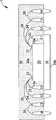
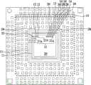
请一并参考图1及图2。图1是依本发明实施例的具有中间端子的QFN半导体封装的剖面示意图。图2是依本发明所述实施例的具有中间端子的QFN半导体封装的布线的上视图。如图1及图2所示,QFN半导体封装1包含具有凹区10a的晶粒附着垫(die attach pad)10。半导体晶粒20附着于晶粒附着垫10的凹区10a中。晶粒附着垫10具有底面10b,其露于模套(moldcap)30之外。晶粒附着垫10可包含电源或接地环11。至少一列内部端子引线12位于靠近晶粒附着垫10的位置。至少一列扩展的外部端子引线14位于沿着QFN半导体封装1外围的位置。至少一列中间端子13位于内部端子引线12与扩展的外部端子引线14之间。依本发明的另一个实施例,晶粒附着垫10可省略。Please refer to Figure 1 and Figure 2 together. FIG. 1 is a schematic cross-sectional view of a QFN semiconductor package with intermediate terminals according to an embodiment of the present invention. 2 is a top view of the wiring of the QFN semiconductor package with intermediate terminals according to the embodiment of the present invention. As shown in FIGS. 1 and 2 , the QFN semiconductor package 1 includes a
半导体晶粒20具有顶面20a,其上有多个键合垫21(包含21a、21b及21c)。半导体晶粒20上的键合垫21a通过金焊线22焊接至电源或接地球环11。半导体晶粒20上的键合垫21b通过金焊线24焊接至内部端子引线12。半导体晶粒20上的键合垫21c通过金焊线26焊接至中间端子13。The semiconductor die 20 has a
依本实施例,外部端子引线14与半导体晶粒的距离超过最大焊线长度,所述最大焊线长度是由焊接工具或焊线机为半导体晶粒的特定的最小焊盘开窗尺寸而提供。如本领域熟悉该项技术的技术人员所知,焊线机所提供的最大焊线长度取决于晶粒上键合垫的最小焊盘开窗尺寸。According to this embodiment, the distance between the external terminal leads 14 and the semiconductor die exceeds the maximum bonding wire length, which is provided by the bonding tool or wire bonding machine for the specific minimum pad opening size of the semiconductor die. . As known to those skilled in the art, the maximum wire length provided by the wire bonder depends on the minimum pad opening size of the bonding pad on the die.
举例来说,对于具有最小焊盘开窗尺寸为43微米(micrometer)的键合垫21来说,典型的焊线机仅可提供140密耳(mil)的最大焊线长度,即3556微米。依本发明的实施例,金焊线26具有焊线键合工具或焊线机可为特定的最小焊盘开窗尺寸而提供的最大焊线长度。为电性连接键合垫21c与外部端子引线14,中间端子13通过金焊线28焊线键合至外部端子引线14。For example, for a
应可理解,上述单一列的中间端子13的排列或布线仅仅是用于例示目的,其不能视为对本发明的范围的限制。在另一个实施例中,中间端子13可被排列成两列或更多列,或可被排列成相互交错的两列。依本实施例,每一中间端子13所占用的键合面面积比每一外部端子引线14所占用的键合面面积小,而外部端子引线14具有与内部端子引线12大体相同的键合面面积。It should be understood that the above-mentioned arrangement or wiring of the
图2较佳地展现了较小的中间端子13。举例来说,每一内部端子引线12与外部端子引线14的尺寸可为270微米×270微米,而每一中间端子13的尺寸可为150微米×150微米。应可理解,每一中间端子13的键合面面积都必须符合金焊线26与28的焊球(squash ball)的需求,上述焊球未在图中明确画出。FIG. 2 preferably shows the smaller
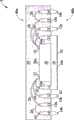
图3是依本发明另一实施例的外部端子引线与中间端子连接的放大上视图。如图3所示,第一列外部端子引线14’通过走线15电性连接至中间端子13’,较远的第二列外部端子引线14”则通过金焊线28电性连接至中间端子13”。Fig. 3 is an enlarged top view of the connection of the external terminal leads and the intermediate terminals according to another embodiment of the present invention. As shown in FIG. 3 , the first column of external terminal leads 14 ′ is electrically connected to the
图4-11是依本发明实施例的用于例示图1所示的具有中间端子的QFN半导体封装的制作方法的剖面示意图,其中相同的标号代表相同的区域、层或元件。如图4所示,提供铜载体40。图样化光阻膜42a及42b分别形成于铜载体40的两个相对面第一面40a及第二面40b之上,以在铜载体40上定义引线阵列图样52及晶粒附着垫图样54。4-11 are cross-sectional schematic diagrams illustrating the fabrication method of the QFN semiconductor package with intermediate terminals shown in FIG. 1 according to an embodiment of the present invention, wherein the same reference numerals represent the same regions, layers or components. As shown in Figure 4, a
如图5所示,执行电镀工艺,以利用可键合金属层62(例如镍、金或其组合)填充铜载体40的两个相对面上的引线阵列图样52及晶粒附着垫图样54。如图6所示,将图样化光阻膜42a及42b剥离以露出铜载体40的表面的一部分。As shown in FIG. 5 , an electroplating process is performed to fill the
如图7所示,接着执行铜蚀刻工艺,以从第一面40a开始半蚀刻铜载体40的露出的部分。在第一面40a上形成凹区10a。在铜蚀刻工艺中,可键合金属层62可作为硬掩膜。依本实施例,图4至7所描述的步骤都可以在导线架制作厂完成。As shown in FIG. 7 , a copper etching process is then performed to half-etch the exposed portion of the
如图8所示,半导体晶粒20附着于凹区10a中,举例来说,可利用表面贴装技术(Surface Mount technology,SMT)或其它适合的方法达成。半导体晶粒20具有顶面20a,顶面20a具有多个键合垫(未明确画出)。As shown in FIG. 8 , the semiconductor die 20 is attached in the
如图9所示,执行焊线键合工艺,以分别通过金焊线22、24、26及28电性连接半导体晶粒20的顶面20a上的键合垫21与对应的端子引线。如前所述,焊线机在焊线键合工艺中提供的最大焊线长度取决于半导体晶粒20上键合垫的最小焊盘开窗尺寸。举例来说,对于具有最小焊盘开窗尺寸为43微米的键合垫来说,典型的焊线机仅可提供140密耳(3556微米)的最大焊线长度。依本实施例,金焊线26具有焊线键合工具或焊线机可为特定的最小焊盘开窗尺寸而提供的最大焊线长度。As shown in FIG. 9 , a wire bonding process is performed to electrically connect the
如图10所示,执行塑模(molding)工艺。金焊线22、24、26及28、半导体晶粒20以及铜载体40的第一面40a被封装在膜套30中,膜套30可例如环氧树脂(epoxy resin)。As shown in FIG. 10, a molding process is performed. The
如图11所示,在塑模工艺之后,执行铜蚀刻工艺以从第二面40b开始半蚀刻铜载体40上未被可键合金属层62覆盖的部分,从而形成晶粒附着垫10、电源或接地环11、内部端子引线12、中间端子13以及外部端子引线14。依本实施例,电源或接地环11可与晶粒附着垫10一起形成,且为环状。电源或接地环11可为连续的或非连续的。晶粒附着垫10、内部端子引线12以及外部端子引线14分别具有大体共面的暴露的底面10b、12b以及14b。暴露的底面10b、12b以及14b最终分别键合至印刷电路板。中间端子13具有凹式底面13b,且凹式底面13b并不与暴露的底面10b、12b以及14b中任何一个共面。依本实施例,图8至11所描述的步骤都可以在组装厂或封装厂完成。As shown in FIG. 11, after the molding process, a copper etching process is performed to half-etch the portion of the
图12是依本发明另一实施例的具有内部端子的QFN半导体封装的剖面示意图。如图12所示,图中QFN半导体封装1a与图1中QFN半导体封装1的区别在于,图12的中间端子13的凹式底面13b被保护层70所覆盖,例如胶粘剂(glue)或其它适合的绝缘材料,以防止与印刷电路板之间发生短路。12 is a schematic cross-sectional view of a QFN semiconductor package with internal terminals according to another embodiment of the present invention. As shown in FIG. 12, the difference between the QFN semiconductor package 1a in the figure and the QFN semiconductor package 1 in FIG. 1 is that the
以上所述仅为本发明的较佳实施例,凡依本发明权利要求所做的均等变化与修饰,皆应属本发明的涵盖范围。The above descriptions are only preferred embodiments of the present invention, and all equivalent changes and modifications made according to the claims of the present invention shall fall within the scope of the present invention.
Claims (22)
Translated fromChineseApplications Claiming Priority (4)
| Application Number | Priority Date | Filing Date | Title |
|---|---|---|---|
| US5417208P | 2008-05-19 | 2008-05-19 | |
| US61/054,172 | 2008-05-19 | ||
| US12/390,492 | 2009-02-22 | ||
| US12/390,492US7786557B2 (en) | 2008-05-19 | 2009-02-22 | QFN Semiconductor package |
Related Parent Applications (1)
| Application Number | Title | Priority Date | Filing Date |
|---|---|---|---|
| CN2009101407334ADivisionCN101587868B (en) | 2008-05-19 | 2009-05-13 | Quad flat no-lead semiconductor package and manufacturing method thereof |
Publications (2)
| Publication Number | Publication Date |
|---|---|
| CN102201385A CN102201385A (en) | 2011-09-28 |
| CN102201385Btrue CN102201385B (en) | 2013-06-12 |
Family
ID=41315378
Family Applications (5)
| Application Number | Title | Priority Date | Filing Date |
|---|---|---|---|
| CN201110108197.7AExpired - Fee RelatedCN102201386B (en) | 2008-05-19 | 2009-05-13 | Quad flat no-lead semiconductor package and manufacturing method thereof |
| CN2011101081892AExpired - Fee RelatedCN102201385B (en) | 2008-05-19 | 2009-05-13 | Quad flat no-lead semiconductor package and manufacturing method thereof |
| CN201110108219XAExpired - Fee RelatedCN102201388B (en) | 2008-05-19 | 2009-05-13 | Quad flat no-lead semiconductor package and manufacturing method thereof |
| CN2009101407334AExpired - Fee RelatedCN101587868B (en) | 2008-05-19 | 2009-05-13 | Quad flat no-lead semiconductor package and manufacturing method thereof |
| CN2011101082170AExpired - Fee RelatedCN102201387B (en) | 2008-05-19 | 2009-05-13 | Quad flat no-lead semiconductor package and manufacturing method thereof |
Family Applications Before (1)
| Application Number | Title | Priority Date | Filing Date |
|---|---|---|---|
| CN201110108197.7AExpired - Fee RelatedCN102201386B (en) | 2008-05-19 | 2009-05-13 | Quad flat no-lead semiconductor package and manufacturing method thereof |
Family Applications After (3)
| Application Number | Title | Priority Date | Filing Date |
|---|---|---|---|
| CN201110108219XAExpired - Fee RelatedCN102201388B (en) | 2008-05-19 | 2009-05-13 | Quad flat no-lead semiconductor package and manufacturing method thereof |
| CN2009101407334AExpired - Fee RelatedCN101587868B (en) | 2008-05-19 | 2009-05-13 | Quad flat no-lead semiconductor package and manufacturing method thereof |
| CN2011101082170AExpired - Fee RelatedCN102201387B (en) | 2008-05-19 | 2009-05-13 | Quad flat no-lead semiconductor package and manufacturing method thereof |
Country Status (3)
| Country | Link |
|---|---|
| US (4) | US7786557B2 (en) |
| CN (5) | CN102201386B (en) |
| TW (1) | TWI385763B (en) |
Families Citing this family (45)
| Publication number | Priority date | Publication date | Assignee | Title |
|---|---|---|---|---|
| US8115285B2 (en)* | 2008-03-14 | 2012-02-14 | Advanced Semiconductor Engineering, Inc. | Advanced quad flat no lead chip package having a protective layer to enhance surface mounting and manufacturing methods thereof |
| US20100015340A1 (en)* | 2008-07-17 | 2010-01-21 | Zenergy Power Inc. | COMPOSITIONS AND METHODS FOR THE MANUFACTURE OF RARE EARTH METAL-Ba2Cu3O7-delta THIN FILMS |
| US20100044850A1 (en) | 2008-08-21 | 2010-02-25 | Advanced Semiconductor Engineering, Inc. | Advanced quad flat non-leaded package structure and manufacturing method thereof |
| US8089145B1 (en)* | 2008-11-17 | 2012-01-03 | Amkor Technology, Inc. | Semiconductor device including increased capacity leadframe |
| US9899349B2 (en) | 2009-01-29 | 2018-02-20 | Semiconductor Components Industries, Llc | Semiconductor packages and related methods |
| US10163766B2 (en) | 2016-11-21 | 2018-12-25 | Semiconductor Components Industries, Llc | Methods of forming leadless semiconductor packages with plated leadframes and wettable flanks |
| US10199311B2 (en) | 2009-01-29 | 2019-02-05 | Semiconductor Components Industries, Llc | Leadless semiconductor packages, leadframes therefor, and methods of making |
| MY163911A (en)* | 2009-03-06 | 2017-11-15 | Shenzhen Standarad Patent & Trademark Agent Ltd | Leadless integrated circuit package having high density contacts |
| US8785253B2 (en) | 2009-04-03 | 2014-07-22 | Kaixin, Inc. | Leadframe for IC package and method of manufacture |
| US8575742B1 (en)* | 2009-04-06 | 2013-11-05 | Amkor Technology, Inc. | Semiconductor device with increased I/O leadframe including power bars |
| US8124447B2 (en) | 2009-04-10 | 2012-02-28 | Advanced Semiconductor Engineering, Inc. | Manufacturing method of advanced quad flat non-leaded package |
| US7993981B2 (en)* | 2009-06-11 | 2011-08-09 | Lsi Corporation | Electronic device package and method of manufacture |
| US20100314728A1 (en)* | 2009-06-16 | 2010-12-16 | Tung Lok Li | Ic package having an inductor etched into a leadframe thereof |
| CN102576701B (en) | 2009-09-02 | 2016-08-17 | 凯信公司 | IC package and method of manufacturing the same |
| MY171813A (en)* | 2009-11-13 | 2019-10-31 | Semiconductor Components Ind Llc | Electronic device including a packaging substrate having a trench |
| TWI479580B (en)* | 2010-03-12 | 2015-04-01 | 矽品精密工業股份有限公司 | Quad flat no-lead package and method for forming the same |
| US8138595B2 (en)* | 2010-03-26 | 2012-03-20 | Stats Chippac Ltd. | Integrated circuit packaging system with an intermediate pad and method of manufacture thereof |
| US8203201B2 (en)* | 2010-03-26 | 2012-06-19 | Stats Chippac Ltd. | Integrated circuit packaging system with leads and method of manufacture thereof |
| CN101853832B (en)* | 2010-04-28 | 2011-12-07 | 江苏长电科技股份有限公司 | Base island exposed type and embedded type base island lead frame structure and first-engraving last-plating method thereof |
| US8860193B2 (en) | 2010-06-04 | 2014-10-14 | Marvell World Trade Ltd. | Pad configurations for an electronic package assembly |
| US8669654B2 (en)* | 2010-08-03 | 2014-03-11 | Stats Chippac Ltd. | Integrated circuit packaging system with die paddle and method of manufacture thereof |
| TWI401755B (en)* | 2010-08-10 | 2013-07-11 | Adl Engineering Inc | Package method for quad flat no-lead package |
| US8552517B1 (en)* | 2010-09-14 | 2013-10-08 | Amkor Technology, Inc. | Conductive paste and mold for electrical connection of photovoltaic die to substrate |
| US8912046B2 (en)* | 2010-10-28 | 2014-12-16 | Stats Chippac Ltd. | Integrated circuit packaging system with lead frame and method of manufacture thereof |
| TWI464852B (en)* | 2010-11-03 | 2014-12-11 | Mediatek Inc | Quad flat no-lead package and board for quad flat no-lead packages |
| US10522518B2 (en)* | 2010-12-23 | 2019-12-31 | Bench Walk Lighting, LLC | Light source with tunable CRI |
| CN102184908A (en)* | 2011-04-26 | 2011-09-14 | 日月光半导体制造股份有限公司 | Advanced quad flat no-lead package structure and manufacturing method thereof |
| US8482109B2 (en)* | 2011-09-22 | 2013-07-09 | Stats Chippac Ltd. | Integrated circuit packaging system with dual connection and method of manufacture thereof |
| CN103107098B (en)* | 2011-11-14 | 2016-05-04 | 美新半导体(无锡)有限公司 | The method for packing of quad flat non-pin and encapsulating structure thereof |
| US8629567B2 (en) | 2011-12-15 | 2014-01-14 | Stats Chippac Ltd. | Integrated circuit packaging system with contacts and method of manufacture thereof |
| US8623711B2 (en)* | 2011-12-15 | 2014-01-07 | Stats Chippac Ltd. | Integrated circuit packaging system with package-on-package and method of manufacture thereof |
| US9219029B2 (en) | 2011-12-15 | 2015-12-22 | Stats Chippac Ltd. | Integrated circuit packaging system with terminals and method of manufacture thereof |
| CN102738019A (en)* | 2012-06-13 | 2012-10-17 | 华天科技(西安)有限公司 | Technology for producing secondary plastic package of AAQFN product on basis of framework carrier open pore and die film |
| CN102738010A (en)* | 2012-06-15 | 2012-10-17 | 华天科技(西安)有限公司 | Technology for producing AAQFN framework product quad flat package on basis of sand blasting |
| US8710636B1 (en) | 2013-02-04 | 2014-04-29 | Freescale Semiconductor, Inc. | Lead frame array package with flip chip die attach |
| US20150084171A1 (en)* | 2013-09-23 | 2015-03-26 | Stmicroelectronics Pte. Ltd. | No-lead semiconductor package and method of manufacturing the same |
| TWI614861B (en)* | 2015-01-30 | 2018-02-11 | 矽品精密工業股份有限公司 | Electronic package structure and the manufacture thereof |
| US9570381B2 (en) | 2015-04-02 | 2017-02-14 | Advanced Semiconductor Engineering, Inc. | Semiconductor packages and related manufacturing methods |
| US9515032B1 (en) | 2015-08-13 | 2016-12-06 | Win Semiconductors Corp. | High-frequency package |
| US9966652B2 (en)* | 2015-11-03 | 2018-05-08 | Amkor Technology, Inc. | Packaged electronic device having integrated antenna and locking structure |
| TW201916182A (en)* | 2017-09-14 | 2019-04-16 | 矽品精密工業股份有限公司 | Electronic package |
| US20200161206A1 (en)* | 2018-11-20 | 2020-05-21 | Advanced Semiconductor Engineering, Inc. | Semiconductor package structure and semiconductor manufacturing process |
| DE102020131070B4 (en) | 2020-11-24 | 2023-03-09 | Infineon Technologies Ag | Package with a raised lead and a structure extending vertically from the bottom of the encapsulant, electronic device, and method of manufacturing a package |
| US11532539B2 (en) | 2020-12-29 | 2022-12-20 | Semiconductor Components Industries, Llc | Semiconductor package with wettable flank |
| IT202300015108A1 (en) | 2023-07-19 | 2025-01-19 | St Microelectronics Int Nv | PROCEDURE FOR MAKING CONNECTIONS IN ELECTRONIC CIRCUITS, CORRESPONDING EQUIPMENT AND COMPUTER PRODUCTS |
Citations (4)
| Publication number | Priority date | Publication date | Assignee | Title |
|---|---|---|---|---|
| US5753970A (en)* | 1993-06-18 | 1998-05-19 | Lsi Logic Corporation | System having semiconductor die mounted in die-receiving area having different shape than die |
| US6906414B2 (en)* | 2000-12-22 | 2005-06-14 | Broadcom Corporation | Ball grid array package with patterned stiffener layer |
| US7060535B1 (en)* | 2003-10-29 | 2006-06-13 | Ns Electronics Bangkok (1993) Ltd. | Flat no-lead semiconductor die package including stud terminals |
| US7361984B2 (en)* | 2006-07-18 | 2008-04-22 | Chipmos Technologies (Shanghai) Ltd. | Chip package structure |
Family Cites Families (15)
| Publication number | Priority date | Publication date | Assignee | Title |
|---|---|---|---|---|
| JPH03167872A (en)* | 1989-11-28 | 1991-07-19 | Seiko Epson Corp | Lead frame semiconductor device |
| WO1998051732A1 (en)* | 1997-05-15 | 1998-11-19 | Chisso Corporation | Unstretched polypropylene molding |
| US6333252B1 (en)* | 2000-01-05 | 2001-12-25 | Advanced Semiconductor Engineering, Inc. | Low-pin-count chip package and manufacturing method thereof |
| US6342730B1 (en)* | 2000-01-28 | 2002-01-29 | Advanced Semiconductor Engineering, Inc. | Low-pin-count chip package and manufacturing method thereof |
| US6261864B1 (en)* | 2000-01-28 | 2001-07-17 | Advanced Semiconductor Engineering, Inc. | Low-pin-count chip package and manufacturing method thereof |
| US6306685B1 (en)* | 2000-02-01 | 2001-10-23 | Advanced Semiconductor Engineering, Inc. | Method of molding a bump chip carrier and structure made thereby |
| US6238952B1 (en)* | 2000-02-29 | 2001-05-29 | Advanced Semiconductor Engineering, Inc. | Low-pin-count chip package and manufacturing method thereof |
| JP4549491B2 (en)* | 2000-03-13 | 2010-09-22 | 大日本印刷株式会社 | Resin-sealed semiconductor device |
| US6507115B2 (en)* | 2000-12-14 | 2003-01-14 | International Business Machines Corporation | Multi-chip integrated circuit module |
| US7132744B2 (en)* | 2000-12-22 | 2006-11-07 | Broadcom Corporation | Enhanced die-up ball grid array packages and method for making the same |
| DE10231385B4 (en)* | 2001-07-10 | 2007-02-22 | Samsung Electronics Co., Ltd., Suwon | Semiconductor chip with bond pads and associated multi-chip package |
| US6621140B1 (en)* | 2002-02-25 | 2003-09-16 | Rf Micro Devices, Inc. | Leadframe inductors |
| US20040178483A1 (en) | 2003-03-12 | 2004-09-16 | Cheng-Ho Hsu | Method of packaging a quad flat no-lead semiconductor and a quad flat no-lead semiconductor |
| DE102004022838A1 (en)* | 2004-05-08 | 2005-12-01 | Forschungszentrum Karlsruhe Gmbh | Ultrasonic transducer and method for producing the same |
| TWI301316B (en)* | 2006-07-05 | 2008-09-21 | Chipmos Technologies Inc | Chip package and manufacturing method threrof |
- 2009
- 2009-02-22USUS12/390,492patent/US7786557B2/enactiveActive
- 2009-05-13TWTW098115827Apatent/TWI385763B/ennot_activeIP Right Cessation
- 2009-05-13CNCN201110108197.7Apatent/CN102201386B/ennot_activeExpired - Fee Related
- 2009-05-13CNCN2011101081892Apatent/CN102201385B/ennot_activeExpired - Fee Related
- 2009-05-13CNCN201110108219XApatent/CN102201388B/ennot_activeExpired - Fee Related
- 2009-05-13CNCN2009101407334Apatent/CN101587868B/ennot_activeExpired - Fee Related
- 2009-05-13CNCN2011101082170Apatent/CN102201387B/ennot_activeExpired - Fee Related
- 2010
- 2010-07-21USUS12/840,304patent/US8039933B2/enactiveActive
- 2010-07-21USUS12/840,308patent/US8039319B2/enactiveActive
- 2010-07-21USUS12/840,307patent/US8044496B2/enactiveActive
Patent Citations (4)
| Publication number | Priority date | Publication date | Assignee | Title |
|---|---|---|---|---|
| US5753970A (en)* | 1993-06-18 | 1998-05-19 | Lsi Logic Corporation | System having semiconductor die mounted in die-receiving area having different shape than die |
| US6906414B2 (en)* | 2000-12-22 | 2005-06-14 | Broadcom Corporation | Ball grid array package with patterned stiffener layer |
| US7060535B1 (en)* | 2003-10-29 | 2006-06-13 | Ns Electronics Bangkok (1993) Ltd. | Flat no-lead semiconductor die package including stud terminals |
| US7361984B2 (en)* | 2006-07-18 | 2008-04-22 | Chipmos Technologies (Shanghai) Ltd. | Chip package structure |
Non-Patent Citations (1)
| Title |
|---|
| JP平3-167872A 1991.07.19 |
Also Published As
| Publication number | Publication date |
|---|---|
| CN102201388B (en) | 2013-01-02 |
| CN102201387A (en) | 2011-09-28 |
| US20100283136A1 (en) | 2010-11-11 |
| CN102201385A (en) | 2011-09-28 |
| CN102201386A (en) | 2011-09-28 |
| CN101587868A (en) | 2009-11-25 |
| US20100285638A1 (en) | 2010-11-11 |
| CN102201387B (en) | 2013-11-13 |
| US20090283882A1 (en) | 2009-11-19 |
| US8039933B2 (en) | 2011-10-18 |
| US20100283137A1 (en) | 2010-11-11 |
| TW200950013A (en) | 2009-12-01 |
| CN102201386B (en) | 2014-04-16 |
| US7786557B2 (en) | 2010-08-31 |
| US8039319B2 (en) | 2011-10-18 |
| US8044496B2 (en) | 2011-10-25 |
| CN101587868B (en) | 2011-07-27 |
| CN102201388A (en) | 2011-09-28 |
| TWI385763B (en) | 2013-02-11 |
Similar Documents
| Publication | Publication Date | Title |
|---|---|---|
| CN102201385B (en) | Quad flat no-lead semiconductor package and manufacturing method thereof | |
| US7932586B2 (en) | Leadframe on heat sink (LOHS) semiconductor packages and fabrication methods thereof | |
| US8836101B2 (en) | Multi-chip semiconductor packages and assembly thereof | |
| US8487424B2 (en) | Routable array metal integrated circuit package fabricated using partial etching process | |
| KR101622805B1 (en) | Leadless array plastic package with various ic packaging configurations | |
| US20110042794A1 (en) | Qfn semiconductor package and circuit board structure adapted for the same | |
| US20090020859A1 (en) | Quad flat package with exposed common electrode bars | |
| US20080308951A1 (en) | Semiconductor package and fabrication method thereof | |
| US20090206459A1 (en) | Quad flat non-leaded package structure | |
| US7298026B2 (en) | Large die package and method for the fabrication thereof | |
| US20100295160A1 (en) | Quad flat package structure having exposed heat sink, electronic assembly and manufacturing methods thereof | |
| US20040021231A1 (en) | Semiconductor device and its manufacturing method | |
| CN102468261B (en) | Quad Flat No-Lead Package and Its Compatible Circuit Board | |
| CN113937074B (en) | Quad Flat No-Lead Package Structure | |
| KR100891649B1 (en) | Semiconductor Package Manufacturing Method | |
| US12125780B2 (en) | Extendable inner lead for leaded package | |
| US20010001069A1 (en) | Metal stud array packaging | |
| KR20020049821A (en) | chip scale semiconductor package in wafer level and method for fabricating the same | |
| KR20010054002A (en) | stack type semiconductor package and method for manucture of the same | |
| KR20040048451A (en) | method for fabricating semiconductor package |
Legal Events
| Date | Code | Title | Description |
|---|---|---|---|
| C06 | Publication | ||
| PB01 | Publication | ||
| C10 | Entry into substantive examination | ||
| SE01 | Entry into force of request for substantive examination | ||
| C14 | Grant of patent or utility model | ||
| GR01 | Patent grant | ||
| CF01 | Termination of patent right due to non-payment of annual fee | Granted publication date:20130612 | |
| CF01 | Termination of patent right due to non-payment of annual fee |