CN102197554A - Monochromatic light source - Google Patents
Monochromatic light sourceDownload PDFInfo
- Publication number
- CN102197554A CN102197554ACN2009801429562ACN200980142956ACN102197554ACN 102197554 ACN102197554 ACN 102197554ACN 2009801429562 ACN2009801429562 ACN 2009801429562ACN 200980142956 ACN200980142956 ACN 200980142956ACN 102197554 ACN102197554 ACN 102197554A
- Authority
- CN
- China
- Prior art keywords
- light
- wavelength
- cases
- light source
- electroluminescent device
- Prior art date
- Legal status (The legal status is an assumption and is not a legal conclusion. Google has not performed a legal analysis and makes no representation as to the accuracy of the status listed.)
- Pending
Links
- 239000004065semiconductorSubstances0.000claimsabstractdescription102
- 230000003287optical effectEffects0.000claimsabstractdescription45
- 230000001427coherent effectEffects0.000claimsdescription17
- SBIBMFFZSBJNJF-UHFFFAOYSA-Nselenium;zincChemical compound[Se]=[Zn]SBIBMFFZSBJNJF-UHFFFAOYSA-N0.000claimsdescription12
- 239000010410layerSubstances0.000description111
- 239000000758substrateSubstances0.000description25
- 238000000034methodMethods0.000description24
- 229910045601alloyInorganic materials0.000description16
- 239000000956alloySubstances0.000description16
- 239000000463materialSubstances0.000description16
- 239000000969carrierSubstances0.000description9
- 229910052751metalInorganic materials0.000description9
- 239000002184metalSubstances0.000description9
- 239000002019doping agentSubstances0.000description7
- IJGRMHOSHXDMSA-UHFFFAOYSA-NAtomic nitrogenChemical compoundN#NIJGRMHOSHXDMSA-UHFFFAOYSA-N0.000description6
- 239000006096absorbing agentSubstances0.000description6
- 230000000903blocking effectEffects0.000description6
- 238000006243chemical reactionMethods0.000description6
- 229910052757nitrogenInorganic materials0.000description6
- 230000001902propagating effectEffects0.000description6
- 239000000853adhesiveSubstances0.000description5
- 230000001070adhesive effectEffects0.000description5
- 238000010276constructionMethods0.000description5
- 238000005530etchingMethods0.000description5
- 238000004519manufacturing processMethods0.000description5
- 230000003595spectral effectEffects0.000description5
- 238000001228spectrumMethods0.000description5
- 238000005229chemical vapour depositionMethods0.000description4
- 239000003086colorantSubstances0.000description4
- 238000005240physical vapour depositionMethods0.000description4
- 229910052782aluminiumInorganic materials0.000description3
- 230000005540biological transmissionEffects0.000description3
- 229910052793cadmiumInorganic materials0.000description3
- 150000001875compoundsChemical class0.000description3
- 238000010586diagramMethods0.000description3
- 239000000203mixtureSubstances0.000description3
- 230000006798recombinationEffects0.000description3
- 238000005215recombinationMethods0.000description3
- 239000000126substanceSubstances0.000description3
- 230000007704transitionEffects0.000description3
- 238000000927vapour-phase epitaxyMethods0.000description3
- 229910000980Aluminium gallium arsenideInorganic materials0.000description2
- 239000004831Hot glueSubstances0.000description2
- 238000003491arrayMethods0.000description2
- 229910052790berylliumInorganic materials0.000description2
- 230000015572biosynthetic processEffects0.000description2
- 229910052794bromiumInorganic materials0.000description2
- 229910052801chlorineInorganic materials0.000description2
- 239000000460chlorineSubstances0.000description2
- 230000007547defectEffects0.000description2
- 238000009792diffusion processMethods0.000description2
- 229910052733galliumInorganic materials0.000description2
- 239000011521glassSubstances0.000description2
- 229910052740iodineInorganic materials0.000description2
- 238000004943liquid phase epitaxyMethods0.000description2
- 229910052749magnesiumInorganic materials0.000description2
- 229910052594sapphireInorganic materials0.000description2
- 239000010980sapphireSubstances0.000description2
- HBMJWWWQQXIZIP-UHFFFAOYSA-Nsilicon carbideChemical compound[Si+]#[C-]HBMJWWWQQXIZIP-UHFFFAOYSA-N0.000description2
- 229910010271silicon carbideInorganic materials0.000description2
- 229910052717sulfurInorganic materials0.000description2
- 229910052714telluriumInorganic materials0.000description2
- 229910052725zincInorganic materials0.000description2
- ZCYVEMRRCGMTRW-UHFFFAOYSA-N7553-56-2Chemical compound[I]ZCYVEMRRCGMTRW-UHFFFAOYSA-N0.000description1
- NIXOWILDQLNWCW-UHFFFAOYSA-MAcrylateChemical compound[O-]C(=O)C=CNIXOWILDQLNWCW-UHFFFAOYSA-M0.000description1
- VHUUQVKOLVNVRT-UHFFFAOYSA-NAmmonium hydroxideChemical compound[NH4+].[OH-]VHUUQVKOLVNVRT-UHFFFAOYSA-N0.000description1
- 241000226585Antennaria plantaginifoliaSpecies0.000description1
- 229910004261CaF 2Inorganic materials0.000description1
- ZAMOUSCENKQFHK-UHFFFAOYSA-NChlorine atomChemical compound[Cl]ZAMOUSCENKQFHK-UHFFFAOYSA-N0.000description1
- 229920001651CyanoacrylatePolymers0.000description1
- 229910001218Gallium arsenideInorganic materials0.000description1
- JMASRVWKEDWRBT-UHFFFAOYSA-NGallium nitrideChemical compound[Ga]#NJMASRVWKEDWRBT-UHFFFAOYSA-N0.000description1
- MWCLLHOVUTZFKS-UHFFFAOYSA-NMethyl cyanoacrylateChemical compoundCOC(=O)C(=C)C#NMWCLLHOVUTZFKS-UHFFFAOYSA-N0.000description1
- -1Si 3 N 4Inorganic materials0.000description1
- 229910004298SiO 2Inorganic materials0.000description1
- 229910010413TiO 2Inorganic materials0.000description1
- QQWICBKIBSOBIT-WXUKJITCSA-N[(e)-2-(4-bicyclo[4.2.0]octa-1(6),2,4-trienyl)ethenyl]-[[(e)-2-(4-bicyclo[4.2.0]octa-1(6),2,4-trienyl)ethenyl]-dimethylsilyl]oxy-dimethylsilaneChemical compoundC1=C2CCC2=CC(/C=C/[Si](C)(O[Si](C)(C)\C=C\C=2C=C3CCC3=CC=2)C)=C1QQWICBKIBSOBIT-WXUKJITCSA-N0.000description1
- 238000010521absorption reactionMethods0.000description1
- 229920006397acrylic thermoplasticPolymers0.000description1
- 230000003044adaptive effectEffects0.000description1
- 238000004026adhesive bondingMethods0.000description1
- 239000012790adhesive layerSubstances0.000description1
- 230000004075alterationEffects0.000description1
- 235000011114ammonium hydroxideNutrition0.000description1
- 230000003321amplificationEffects0.000description1
- 230000004888barrier functionEffects0.000description1
- 230000008901benefitEffects0.000description1
- UMIVXZPTRXBADB-UHFFFAOYSA-NbenzocyclobuteneChemical classC1=CC=C2CCC2=C1UMIVXZPTRXBADB-UHFFFAOYSA-N0.000description1
- UHYPYGJEEGLRJD-UHFFFAOYSA-Ncadmium(2+);selenium(2-)Chemical compound[Se-2].[Cd+2]UHYPYGJEEGLRJD-UHFFFAOYSA-N0.000description1
- 235000012215calcium aluminium silicateNutrition0.000description1
- 239000000404calcium aluminium silicateSubstances0.000description1
- WNCYAPRTYDMSFP-UHFFFAOYSA-Ncalcium aluminosilicateChemical compound[Al+3].[Al+3].[Ca+2].[O-][Si]([O-])=O.[O-][Si]([O-])=O.[O-][Si]([O-])=O.[O-][Si]([O-])=OWNCYAPRTYDMSFP-UHFFFAOYSA-N0.000description1
- 229940078583calcium aluminosilicateDrugs0.000description1
- 238000005253claddingMethods0.000description1
- 238000000151depositionMethods0.000description1
- 229910003460diamondInorganic materials0.000description1
- 239000010432diamondSubstances0.000description1
- 238000001312dry etchingMethods0.000description1
- 230000000694effectsEffects0.000description1
- 238000000295emission spectrumMethods0.000description1
- 230000002708enhancing effectEffects0.000description1
- 239000000835fiberSubstances0.000description1
- 229910052731fluorineInorganic materials0.000description1
- 229910052737goldInorganic materials0.000description1
- 229910052738indiumInorganic materials0.000description1
- 230000010354integrationEffects0.000description1
- 239000011630iodineSubstances0.000description1
- 230000001788irregularEffects0.000description1
- 238000005304joiningMethods0.000description1
- 230000031700light absorptionEffects0.000description1
- 239000007788liquidSubstances0.000description1
- 229910044991metal oxideInorganic materials0.000description1
- 150000004706metal oxidesChemical class0.000description1
- 238000004377microelectronicMethods0.000description1
- 230000004048modificationEffects0.000description1
- 238000012986modificationMethods0.000description1
- 238000001451molecular beam epitaxyMethods0.000description1
- 238000003199nucleic acid amplification methodMethods0.000description1
- 239000013307optical fiberSubstances0.000description1
- 238000000206photolithographyMethods0.000description1
- 238000001020plasma etchingMethods0.000description1
- 229920003229poly(methyl methacrylate)Polymers0.000description1
- 229920000728polyesterPolymers0.000description1
- 229920000098polyolefinPolymers0.000description1
- 235000019353potassium silicateNutrition0.000description1
- 238000003825pressingMethods0.000description1
- 230000008569processEffects0.000description1
- 238000013139quantizationMethods0.000description1
- 238000002310reflectometryMethods0.000description1
- 230000004044responseEffects0.000description1
- 239000000565sealantSubstances0.000description1
- 229910052711seleniumInorganic materials0.000description1
- 238000000926separation methodMethods0.000description1
- 229910052709silverInorganic materials0.000description1
- NTHWMYGWWRZVTN-UHFFFAOYSA-Nsodium silicateChemical compound[Na+].[Na+].[O-][Si]([O-])=ONTHWMYGWWRZVTN-UHFFFAOYSA-N0.000description1
- 238000005476solderingMethods0.000description1
- 238000003756stirringMethods0.000description1
- 230000001629suppressionEffects0.000description1
- ISXSCDLOGDJUNJ-UHFFFAOYSA-Ntert-butyl prop-2-enoateChemical compoundCC(C)(C)OC(=O)C=CISXSCDLOGDJUNJ-UHFFFAOYSA-N0.000description1
- 229920001169thermoplasticPolymers0.000description1
- 239000004416thermosoftening plasticSubstances0.000description1
- 238000007740vapor depositionMethods0.000description1
- XLYOFNOQVPJJNP-UHFFFAOYSA-NwaterSubstancesOXLYOFNOQVPJJNP-UHFFFAOYSA-N0.000description1
- 239000001993waxSubstances0.000description1
- 238000003466weldingMethods0.000description1
- 238000001039wet etchingMethods0.000description1
Images


Classifications
- H—ELECTRICITY
- H01—ELECTRIC ELEMENTS
- H01S—DEVICES USING THE PROCESS OF LIGHT AMPLIFICATION BY STIMULATED EMISSION OF RADIATION [LASER] TO AMPLIFY OR GENERATE LIGHT; DEVICES USING STIMULATED EMISSION OF ELECTROMAGNETIC RADIATION IN WAVE RANGES OTHER THAN OPTICAL
- H01S5/00—Semiconductor lasers
- H01S5/04—Processes or apparatus for excitation, e.g. pumping, e.g. by electron beams
- H01S5/041—Optical pumping
- H—ELECTRICITY
- H10—SEMICONDUCTOR DEVICES; ELECTRIC SOLID-STATE DEVICES NOT OTHERWISE PROVIDED FOR
- H10H—INORGANIC LIGHT-EMITTING SEMICONDUCTOR DEVICES HAVING POTENTIAL BARRIERS
- H10H20/00—Individual inorganic light-emitting semiconductor devices having potential barriers, e.g. light-emitting diodes [LED]
- H10H20/80—Constructional details
- H10H20/85—Packages
- H10H20/851—Wavelength conversion means
- H10H20/8514—Wavelength conversion means characterised by their shape, e.g. plate or foil
- H—ELECTRICITY
- H10—SEMICONDUCTOR DEVICES; ELECTRIC SOLID-STATE DEVICES NOT OTHERWISE PROVIDED FOR
- H10H—INORGANIC LIGHT-EMITTING SEMICONDUCTOR DEVICES HAVING POTENTIAL BARRIERS
- H10H20/00—Individual inorganic light-emitting semiconductor devices having potential barriers, e.g. light-emitting diodes [LED]
- H10H20/80—Constructional details
- H10H20/85—Packages
- H10H20/851—Wavelength conversion means
- H10H20/8515—Wavelength conversion means not being in contact with the bodies
- H—ELECTRICITY
- H01—ELECTRIC ELEMENTS
- H01S—DEVICES USING THE PROCESS OF LIGHT AMPLIFICATION BY STIMULATED EMISSION OF RADIATION [LASER] TO AMPLIFY OR GENERATE LIGHT; DEVICES USING STIMULATED EMISSION OF ELECTROMAGNETIC RADIATION IN WAVE RANGES OTHER THAN OPTICAL
- H01S5/00—Semiconductor lasers
- H01S5/02—Structural details or components not essential to laser action
- H01S5/024—Arrangements for thermal management
- H01S5/02476—Heat spreaders, i.e. improving heat flow between laser chip and heat dissipating elements
- H—ELECTRICITY
- H01—ELECTRIC ELEMENTS
- H01S—DEVICES USING THE PROCESS OF LIGHT AMPLIFICATION BY STIMULATED EMISSION OF RADIATION [LASER] TO AMPLIFY OR GENERATE LIGHT; DEVICES USING STIMULATED EMISSION OF ELECTROMAGNETIC RADIATION IN WAVE RANGES OTHER THAN OPTICAL
- H01S5/00—Semiconductor lasers
- H01S5/10—Construction or shape of the optical resonator, e.g. extended or external cavity, coupled cavities, bent-guide, varying width, thickness or composition of the active region
- H01S5/18—Surface-emitting [SE] lasers, e.g. having both horizontal and vertical cavities
- H01S5/183—Surface-emitting [SE] lasers, e.g. having both horizontal and vertical cavities having only vertical cavities, e.g. vertical cavity surface-emitting lasers [VCSEL]
- H—ELECTRICITY
- H01—ELECTRIC ELEMENTS
- H01S—DEVICES USING THE PROCESS OF LIGHT AMPLIFICATION BY STIMULATED EMISSION OF RADIATION [LASER] TO AMPLIFY OR GENERATE LIGHT; DEVICES USING STIMULATED EMISSION OF ELECTROMAGNETIC RADIATION IN WAVE RANGES OTHER THAN OPTICAL
- H01S5/00—Semiconductor lasers
- H01S5/40—Arrangement of two or more semiconductor lasers, not provided for in groups H01S5/02 - H01S5/30
- H01S5/42—Arrays of surface emitting lasers
- H01S5/423—Arrays of surface emitting lasers having a vertical cavity
Landscapes
- Physics & Mathematics (AREA)
- Condensed Matter Physics & Semiconductors (AREA)
- General Physics & Mathematics (AREA)
- Electromagnetism (AREA)
- Optics & Photonics (AREA)
- Semiconductor Lasers (AREA)
- Luminescent Compositions (AREA)
- Electroluminescent Light Sources (AREA)
Abstract
Translated fromChinese
Description
Translated fromChinese技术领域technical field
本发明总体上涉及半导体光源。本发明特别适用于包含一种或多种II-VI半导体化合物的半导体光源。The present invention generally relates to semiconductor light sources. The invention is particularly applicable to semiconductor light sources comprising one or more II-VI semiconductor compounds.
背景技术Background technique
激光二极管被用于许多不同应用,例如激光指示器、投影显示器和传感器。在光谱的近紫外、紫色、近红外或红外区发光的激光二极管可以是小型且低成本的。然而,在光谱的其他区中,已知的激光二极管(例如,倍频激光二极管)是复杂、大型、低效且高成本的。非常需要能够在其他所需波长下(例如,在光谱的青色、绿色、黄绿色、黄色和琥珀色区)发光的小型、高效且低成本的激光二极管系统。Laser diodes are used in many different applications such as laser pointers, projection displays and sensors. Laser diodes emitting in the near ultraviolet, violet, near infrared or infrared regions of the spectrum can be small and low cost. However, in other regions of the spectrum, known laser diodes (eg, frequency doubled laser diodes) are complex, large, inefficient and costly. Small, efficient, and low-cost laser diode systems capable of emitting at other desired wavelengths (for example, in the cyan, green, yellow-green, yellow, and amber regions of the spectrum) are highly desirable.
发明内容Contents of the invention
总体上,本发明涉及半导体光源。在一个实施例中,光源包括基于III-V的泵浦光源,该光源包含氮并发射第一波长的光。光源进一步包括垂直腔面发射激光器(VCSEL),该激光器将由泵浦光源发射的第一波长的光的至少一部分转换为第二波长的至少部分相干光。VCSEL包括形成第二波长的光的共振腔的第一和第二反射镜。第一反射镜在第二波长下大量地反射,并包括第一多层叠堆。第二反射镜在第一波长下大量地透射并在第二波长下部分反射且部分透射。第二反射镜包括第二多层叠堆。VCSEL进一步包括设置在第一和第二反射镜之间并将第一波长的光的至少一部分转换为第二波长的光的半导体多层叠堆。半导体多层叠堆包括含有Cd(Mg)ZnSe合金的量子阱。In general, the present invention relates to semiconductor light sources. In one embodiment, the light source comprises a III-V based pump light source comprising nitrogen and emitting light at a first wavelength. The light source further includes a vertical cavity surface emitting laser (VCSEL) that converts at least a portion of the light emitted by the pump light source at the first wavelength to at least partially coherent light at the second wavelength. The VCSEL includes first and second mirrors forming a resonant cavity for light of the second wavelength. The first mirror is substantially reflective at the second wavelength and includes a first multilayer stack. The second mirror is substantially transmissive at the first wavelength and partially reflective and partially transmissive at the second wavelength. The second mirror includes a second multilayer stack. The VCSEL further includes a semiconductor multilayer stack disposed between the first and second mirrors and converting at least a portion of the light at the first wavelength to light at the second wavelength. The semiconductor multilayer stack includes quantum wells comprising a Cd(Mg)ZnSe alloy.
在另一实施例中,光源包括基于III-V的泵浦光源,该光源包含氮并发射第一波长的光。光源进一步包括光学组件,该组件将由泵浦光源发射的第一波长的光转换为第二波长的至少部分相干光。光学组件包括形成第二波长的光的共振腔的第一和第二反射镜。第一反射镜在第二波长下大量地反射,并包括第一多层叠堆。第二反射镜在第二波长下部分地反射。光学组件进一步包括设置在第一和第二反射镜之间并将第一波长的光的至少一部分转换为第二波长的光的半导体多层叠堆。半导体多层叠堆包括含有Cd(Mg)ZnSe合金的量子阱。In another embodiment, the light source comprises a III-V based pump light source comprising nitrogen and emitting light at a first wavelength. The light source further includes an optical component that converts light at the first wavelength emitted by the pump light source to at least partially coherent light at a second wavelength. The optical assembly includes first and second mirrors forming a resonant cavity for light of the second wavelength. The first mirror is substantially reflective at the second wavelength and includes a first multilayer stack. The second mirror is partially reflective at the second wavelength. The optical assembly further includes a semiconductor multilayer stack disposed between the first and second mirrors and converting at least a portion of the light at the first wavelength to light at the second wavelength. The semiconductor multilayer stack includes quantum wells comprising a Cd(Mg)ZnSe alloy.
在另一实施例中,发光系统包括发射第一波长的光的电致发光装置。发光系统还包括增强从发光系统的顶面的光发射并抑制从发光系统的一个或多个侧面的光发射的共振腔。光腔包括可接收所发射的第一波长的光并将接收光的至少一部分转换为第二波长的光的半导体多层叠堆。半导体多层叠堆包括II-VI势阱。离开发光系统的第二波长所有光的积分发光强度为离开发光系统的第一波长所有光的积分发光强度的至少10倍。在一些情况下,II-VI势阱包括Cd(Mg)ZnSe或ZnSeTe。在一些情况下,电致发光装置被设计成使得半导体多层叠堆接收的第一波长的光的大部分通过电致发光装置的顶面离开电致发光装置。在一些情况下,由发光系统沿第一方向发射的光具有第一组色坐标,由发光系统沿不同于第一方向的第二方向发射的光具有第二组色坐标,其中第二组色坐标与第一组色坐标基本相同。在一些情况下,第一组色坐标是u1’和v1’,第二组色坐标是u2’和v2’,u1’和u2’之间以及v1’和v2’之间差值中每一个的绝对值不超过0.003。在一些情况下,再发射的第二波长的光的主要部分从发光系统的顶面离开发光系统。顶面具有最小横向尺寸Wmin再发射的第二波长的光的剩余部分的大部分从具有最大边缘厚度Tmax的光腔的一个或多个侧面离开发光系统。比率Wmin/Tmax至少约为30。发射的第一波长的光的主要部分从电致发光装置的顶面离开电致发光装置。顶面具有最小的横向尺寸W1min。发射的第一波长的光的剩余部分从具有最大边缘厚度T1max的电致发光装置的一个或多个侧面离开电致发光装置。比率W1min/T1max至少约为30。在一些情况下,比率Wmin/Tmax和W1min/T1max各自至少为约100。In another embodiment, the light emitting system includes an electroluminescent device that emits light at a first wavelength. The light emitting system also includes a resonant cavity that enhances light emission from the top surface of the light emitting system and suppresses light emission from one or more sides of the light emitting system. The optical cavity includes a semiconductor multilayer stack operable to receive emitted light at a first wavelength and convert at least a portion of the received light to light at a second wavelength. The semiconductor multilayer stack includes II-VI potential wells. The integrated luminous intensity of all light at the second wavelength exiting the light emitting system is at least 10 times the integrated luminous intensity of all light at the first wavelength exiting the light emitting system. In some cases, the II-VI potential well includes Cd(Mg)ZnSe or ZnSeTe. In some cases, the electroluminescent device is designed such that a substantial portion of light at the first wavelength received by the semiconductor multilayer stack exits the electroluminescent device through a top surface of the electroluminescent device. In some cases, light emitted by the light emitting system in a first direction has a first set of color coordinates, and light emitted by the light emitting system in a second direction different from the first direction has a second set of color coordinates, wherein the second set of color coordinates The coordinates are basically the same as the first set of color coordinates. In some cases, the first set of color coordinates is u1 ' and v1 ', the second set of color coordinates is u2 ' and v2 ', between u1 ' and u2 ' and between v1 ' and v2 ' The absolute value of each of the differences between is not more than 0.003. In some cases, a substantial portion of the re-emitted second wavelength light exits the light emitting system from the top surface of the light emitting system. A substantial portion of the remaining portion of the light of the second wavelength re-emitted by the top surface having the smallest lateral dimension Wmin exits the light emitting system from one or more sides of the optical cavity having the largest edge thickness Tmax . The ratio Wmin /Tmax is at least about 30. A substantial portion of the emitted light of the first wavelength exits the electroluminescent device from the top surface of the electroluminescent device. The top surface has the smallest lateral dimension W1min . The remainder of the emitted light of the first wavelength exits the electroluminescent device from one or more sides of the electroluminescent device having a maximum edge thickness T1max . The ratio W1min /T1max is at least about 30. In some cases, the ratios Wmin /Tmax and W1min /T1max are each at least about 100.
附图说明Description of drawings
结合附图对本发明的各种实施例所做的以下详细描述将有利于更完整地理解和体会本发明,其中:The following detailed description of various embodiments of the present invention in conjunction with the accompanying drawings will facilitate a more complete understanding and appreciation of the present invention, wherein:
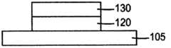
图1是光源的示意性侧视图;Figure 1 is a schematic side view of a light source;
图2是包括离散光源阵列的光源的示意性侧视图;Figure 2 is a schematic side view of a light source comprising an array of discrete light sources;
图3A-3E是处于用于制造光源的方法中的中间阶段或步骤的装置的示意图;3A-3E are schematic diagrams of devices at intermediate stages or steps in a method for manufacturing a light source;
图4是另一光源的示意性侧视图;Figure 4 is a schematic side view of another light source;
图5是另一光源的示意性侧视图;5 is a schematic side view of another light source;
图6是发光系统的示意性侧视图;和Figure 6 is a schematic side view of a lighting system; and
图7是光指示器的示意图。Figure 7 is a schematic diagram of a light pointer.
多个图中使用的相同附图标记指代具有相同或相似性能和功能的相同或相似元件。The same reference numerals used in multiple figures refer to the same or similar elements having the same or similar properties and functions.
具体实施方式Detailed ways
本申请公开了半导体光源,其包括一个或多个泵浦光源和用于将由泵浦光源发射的光转换为不同波长光的一个或多个半导体光腔。在一些情况下,所公开的半导体光腔是能够将入射光变频(例如下变频)的共振腔。在一些情况下,所公开的半导体共振腔波长转换器是垂直腔面发射激光器(VCSEL)。所公开的光源是高效、小型的,并且在一些情况下,将光转换VCSEL与由两个或更多个不同半导体组构成的泵浦光源低成本地集成。例如,本申请公开了一种光源,其将III-V泵浦光源(例如,包括N的泵浦光源,例如AlGaInN泵浦LED或激光二极管)与包括II-VI半导体波长转换器(例如,Cd(Mg)ZnSe波长转换器)的II-VI VCSEL集成。The present application discloses a semiconductor light source, which includes one or more pump light sources and one or more semiconductor optical cavities for converting light emitted by the pump light sources into light of different wavelengths. In some cases, the disclosed semiconductor optical cavities are resonant cavities capable of frequency converting (eg, down converting) incident light. In some cases, the disclosed semiconductor resonator wavelength converters are vertical cavity surface emitting lasers (VCSELs). The disclosed light sources are efficient, compact, and in some cases cost-effectively integrate a light-converting VCSEL with a pump light source composed of two or more different semiconductor groups. For example, the present application discloses a light source that combines a III-V pump light source (e.g., a pump light source comprising N, such as an AlGaInN pump LED or a laser diode) with a II-VI semiconductor wavelength converter (e.g., a Cd (Mg)ZnSe wavelength converter) II-VI VCSEL integration.
在一些情况下,泵浦光源例如激光二极管(LD)光源至少为部分相干光源,这意味着其发射至少部分相干的光。在一些情况下,泵浦光源例如发光二极管(LED)光源是非相干光源,这意味着其发射非相干光。In some cases, the pump light source, such as a laser diode (LD) light source, is at least partially coherent, meaning that it emits at least partially coherent light. In some cases, the pump light source, such as a light emitting diode (LED) light source, is an incoherent light source, meaning that it emits incoherent light.
在一些情况下,半导体VCSEL和泵浦光源来自同一个半导体组,例如III-V组。在此类情况下,直接将例如III-V VCSEL单块生长并制造到III-V泵浦光源(例如,III-V泵浦)是可行的。然而,在一些情况下,发射所需波长光并具有高转换效率和/或其他所需特性的VCSEL来自不同于泵浦LD或LED所属组的半导体组。例如,VCSEL可来自II-VI组,而光源例如LD或LED可来自III-V组。在这种情况下,以高品质将一个元件生长到另一元件上可能是不可能或不可行的。在这种情况下,VCSEL可以附接到泵浦光源来形成混合光源。此类混合光源能够以高的总体效率发射例如在光谱可见区中不同波长的光。2007年10月8日提交的美国专利申请No.60/978304描述了附接两种构造的示例性方法,其全文以引用方式并入本文。In some cases, the semiconductor VCSEL and the pump light source are from the same semiconductor group, eg III-V group. In such cases, it is feasible to monolithically grow and fabricate, for example, a III-V VCSEL directly to a III-V pump source (eg, III-V pump). In some cases, however, the VCSELs that emit light at the desired wavelength and have high conversion efficiency and/or other desired characteristics are from a different group of semiconductors than the group to which the pump LD or LED belongs. For example, VCSELs may be from group II-VI, while light sources such as LDs or LEDs may be from group III-V. In such cases, it may not be possible or feasible to grow one element onto another with high quality. In this case, a VCSEL can be attached to the pump light source to form a hybrid light source. Such hybrid light sources are capable of emitting light of different wavelengths, for example in the visible region of the spectrum, with high overall efficiency. An exemplary method of attaching two configurations is described in US Patent Application No. 60/978304, filed October 8, 2007, which is hereby incorporated by reference in its entirety.
在一些情况下,所公开的光源可以输出例如一种或多种原色,例如RGB原色系统中的蓝色、绿色或红色,或者CMYK原色系统中的青色、品红和黄色。在一些情况下,所公开的光源可以输出具有其他颜色(例如琥珀色或白色)的光。所公开的光源的发射效率和紧凑度可以导致新改进的光学系统,例如重量、尺寸和功耗降低的高效投影系统。In some cases, the disclosed light sources can output, for example, one or more primary colors, such as blue, green, or red in the RGB primary color system, or cyan, magenta, and yellow in the CMYK primary color system. In some cases, the disclosed light sources may output light having other colors, such as amber or white. The emission efficiency and compactness of the disclosed light sources can lead to new and improved optical systems such as efficient projection systems with reduced weight, size and power consumption.
在一些情况下,VCSEL可以包括将光转换为更长波长光的势阱或量子阱,例如半导体势阱或量子阱。在一些情况下,所公开的光源将来自半导体组(例如II-VI组)的一个或多个VCSEL与来自不同半导体组(例如III-V组)的一个或多个泵浦光源(例如泵浦LD或LED)高效地集成。In some cases, a VCSEL may include a potential or quantum well, such as a semiconductor potential or quantum well, that converts light to longer wavelength light. In some cases, the disclosed light sources combine one or more VCSELs from a semiconductor group (e.g., group II-VI) with one or more pump light sources (e.g., pump LD or LED) are efficiently integrated.
所公开的光源阵列包括泵浦光源阵列和对应的VCSEL阵列。这样的光源阵列可以形成单色(例如,绿色或绿黑色)或彩色图像。所公开的光源阵列可以结合常规光源和图像形成装置的主要功能,从而导致功耗、尺寸和成本减少。例如,在显示系统中,所公开的光源阵列可以同时用作光源和图像形成装置,从而消除或减少对单独背光或空间光调制器的需要。又如,将所公开的光源阵列并入投影系统可消除或减少对图像形成装置和中继器光学器件的需要。The disclosed light source array includes a pump light source array and a corresponding VCSEL array. Such arrays of light sources can form monochrome (eg, green or green-black) or color images. The disclosed light source array can combine the primary functions of conventional light sources and image forming devices, resulting in reduced power consumption, size and cost. For example, in a display system, the disclosed array of light sources can be used as both a light source and an image forming device, thereby eliminating or reducing the need for a separate backlight or spatial light modulator. As another example, incorporating the disclosed array of light sources into a projection system can eliminate or reduce the need for image forming devices and repeater optics.
例如,所公开的光源阵列可以在显示系统中形成像素阵列。光源的至少一些包括能够响应电信号而发光的泵浦电致发光装置,例如泵浦LD或LED。光源的至少一些可以包括一个或多个VCSEL,VCSEL包括用于将泵浦电致发光装置发出的光下变频的一个或多个光转换元件,例如一个或多个势阱和/或量子阱。如本文所用,下变频意指被变频光的光子能量低于泵浦光的光子能量,或者被变频光的波长长于未变频光即入射光的波长。For example, the disclosed array of light sources can form an array of pixels in a display system. At least some of the light sources include pumped electroluminescent devices, such as pumped LDs or LEDs, capable of emitting light in response to an electrical signal. At least some of the light sources may comprise one or more VCSELs comprising one or more light conversion elements, such as one or more potential wells and/or quantum wells, for downconverting light emitted by the pump electroluminescent device. As used herein, down-converted means that the photon energy of the converted light is lower than that of the pump light, or that the wavelength of the converted light is longer than that of the unconverted light, ie, the incident light.
例如,所公开的光源阵列可以用于在例如投影系统或其他光学系统中使用的照明系统,例如自适应照明系统。For example, the disclosed light source arrays may be used in lighting systems, such as adaptive lighting systems, used in, for example, projection systems or other optical systems.
图1是包括基于III-V的泵浦光源170的光源100的示意性侧视图,该基于III-V的泵浦光源包括氮N并发射第一波长λ1的光172。在一些情况下,光源170具有带有一个或多个峰值的发射光谱,波长λ1为峰值发射的波长。在一些情况下,光源170发射基本上为单波长λ1的光,这意味着所发射的光谱具有λ1的窄峰和小的半峰全宽(FWHM)。在这类情况下,FWHM可以小于约50nm、小于约10nm、小于约5nm或小于约1nm。在一些情况下,泵浦光源是III-V激光二极管。在一些情况下,泵浦波长λ1在约350nm和约500nm之间。例如,在一些情况下,λ1可以约为405nm。1 is a schematic side view of a light source 100 comprising a III-V based pump
光源100还包括垂直腔面发射激光器(VCSEL)190,其将由泵浦光源170发射的第一波长的光172的至少一部分转换为第二波长λ2的至少部分相干输出光178。The light source 100 also includes a vertical cavity surface emitting laser (VCSEL) 190 that converts at least a portion of the light 172 at the first wavelength emitted by the pump
VCSEL 190包括形成第二波长的光的共振腔的第一反射镜120和第二反射镜160。在一些情况下,光腔的光学厚度可以是第二波长λ2一半的奇数倍(也就是说,(2m+1)(λ2/2),其中m是整数)。在这类情况下,光腔内λ2的光驻波的节点位于或靠近光腔的中心。在一些情况下,光腔的光学厚度可以是第二波长λ2的整数倍(也就是说,mλ2,其中m是整数)。在这类情况下,光腔内λ2的光驻波的腹点位于或靠近光腔的中心。The
在一些情况下,第一反射镜120在第二波长下大量地反射。例如,在这类情况下,在第二波长λ2下第一反射镜120的反射率为至少80%、至少90%、至少95%、至少99%、至少99.5%或至少99.9%。在一些情况下,第一反射镜120在第一波长λ1下大量地透射。例如,在这类情况下,在λ1下第一反射镜120的光透射率为至少50%、至少60%、至少70%、至少80或至少90%。In some cases,
在一些情况下,例如在图1所示的示例性光源100中,第一反射镜120是(或包括)第一布拉格反射镜120。布拉格反射镜包括由具有较低折射率的低折射率层122和具有较高折射率的高折射率层124交替构成的多层叠堆。在示例性光源100中,第一布拉格反射镜120包括四层低折射率层122和四层高折射率层124。通常,第一布拉格反射镜120可以包括一层或多层低折射率层122和一层或多层高折射率层124。例如,在一些情况下,第一布拉格反射镜120可以具有至少5层低折射率层和5层高折射率层、至少10层低折射率层和10层高折射率层、或至少15层低折射率层和15层高折射率层。In some cases, such as in the exemplary light source 100 shown in FIG. 1 , the
在一些情况下,第一布拉格反射镜120中低和/或高折射率层的至少一些的光学厚度是该层中第二波长的四分之一。在这类情况下,对四分之一波厚层而言,物理厚度为λ2/4n,其中n是λ2下该层的折射率。In some cases, the optical thickness of at least some of the low and/or high index layers in
第一布拉格反射镜120可以包括具有合适的较低和较高折射率的任何材料。示例性材料包括SiO2、Si3N4、TiO2、Ta2O5、MgF2、CaF2和HfO2。在一些情况下,第一布拉格反射镜120可以包括II-VI材料,例如ZnSe、ZnS、Cd(Mg)ZnSe、Mg(Zn)Se或其任意组合或合金。The
在一些情况下,第二反射镜160在第二波长λ2下部分地反射。在这类情况下,在第二波长λ2下第二反射镜160的反射率为至少80%、至少90%、至少95%、至少99%、至少99.5%或至少99.9%。在一些情况下,第二反射镜160在第二波长λ2下部分地透射。在这类情况下,在第二波长下第二反射镜的光透射率不超过5%、不超过3%、不超过2%、不超过1%或不超过0.5%。In some cases,
在一些情况下,例如在图1所示的示例性光源中,第二反射镜160是(或包括)第二布拉格反射镜,该第二布拉格反射镜包括由具有较低折射率的低折射率层162和具有较高折射率的高折射率层164交替构成的多层叠堆。在示例性光源100中,第二布拉格反射镜160包括三层低折射率层162和三层高折射率层164。通常,第二布拉格反射镜160可以包括一层或多层低折射率层162和一层或多层高折射率层164。例如,在一些情况下,第二布拉格反射镜160可以具有至少5层低折射率层和5层高折射率层、至少10层低折射率层和10层高折射率层、或至少15层低折射率层和15层高折射率层。In some cases, such as in the exemplary light source shown in FIG. 1 ,
在一些情况下,第二布拉格反射镜160中低和/或高折射率层的至少一些的光学厚度是该层中第二波长的四分之一。在这类情况下,物理厚度为λ2/4n,其中n是λ2下该层的折射率。In some cases, the optical thickness of at least some of the low and/or high index layers in
光源100进一步包括分别设置在第一和第二反射镜120和160之间的半导体多层叠堆130。多层叠堆130将第一波长的光174的至少一部分转换为第二波长的光176。在一些情况下,光从第一波长到第二波长的转换在半导体多层叠堆130吸收光174的至少一部分并作为第二波长的光176重发吸收光的至少一部分时即可告成。在一些情况下,泵浦光源170可发射紫外光或紫色光,并且半导体多层叠堆130可重发蓝色、绿色、黄色、琥珀色或红色光。在一些情况下,泵浦光源170可发射蓝色光,并且重发光半导体多层叠堆130可重发绿色、黄色、琥珀色或红色光。The light source 100 further includes a
半导体多层叠堆130包括各自的第一和第二窗口132和134,以及包括多个交替的势阱和光吸收层的势阱叠堆。具体地讲,示例性半导体多层叠堆130包括各自的第一、第二和第三吸收层140、142和144;以及各自的第一和第二势阱152和154。
半导体多层叠堆130中的光吸收层吸收第一波长的光174的至少一部分,并且(作为引起的反应)产生光生载流子,例如光生电子-空穴对。载流子从光吸收层扩散到半导体多层叠堆中的相邻势阱,在该处它们复合而辐射出第二波长λ2的光。The light absorbing layer in the
在一些情况下,例如当半导体多层叠堆130中光生电子-空穴对的密度足够高时,第二波长的光176可以随着其在反射镜120和160之间来回传播而放大。放大主要发生在势阱中,其中传播的光借助于第二波长λ2光的受激发射来帮助载流子复合。在这类情况下,如果反射镜120和160在λ2下充分地反射,则反射镜可以有效地增加光176穿过势阱的次数。这样,VCSEL可以产生λ2的相干或至少部分相干光。In some cases, such as when the density of photogenerated electron-hole pairs in
通常,重发光多层叠堆130包括至少一层能够将光(例如蓝色光或紫外光)的至少一部分转换为较长波长的光的II-VI化合物。在一些情况下,II-VI波长转换器包括II-VI势阱或量子阱。Typically, light emitting
如本文所用,势阱是指被设计为仅在一个维度上限制载流子的多层半导体结构中的半导体层,其中所述半导体层具有低于周围层的导带能和/或高于周围层的价带能。量子阱通常是指足够薄从而量子化效应增加用于阱中电子-空穴对复合的能量的势阱。量子阱通常具有约100nm或更小、或者约10nm或更小的厚度。As used herein, a potential well refers to a semiconductor layer in a multilayer semiconductor structure designed to confine carriers in only one dimension, where the semiconductor layer has a conduction band energy lower than that of the surrounding layers and/or higher than that of the surrounding layers. The valence band energy of the layer. A quantum well generally refers to a potential well that is thin enough that quantization effects increase the energy available for recombination of electron-hole pairs in the well. Quantum wells typically have a thickness of about 100 nm or less, or about 10 nm or less.
在一些情况下,势阱或量子阱152和/或154是II-VI半导体势阱或量子阱,其具有比由泵浦光源170发射的光子的能量小的带隙能。通常,势阱或量子阱152和/或154的跃迁能基本上等于由势阱或量子阱再发射的光子的能量。In some cases, potential or quantum wells 152 and/or 154 are II-VI semiconductor potential or quantum wells that have a bandgap energy that is less than the energy of photons emitted by pump
在一些情况下,势阱152和154可以包括以化合物ZnSe、CdSe和MgSe作为合金三种组分的CdMgZnSe合金。在一些情况下,合金中可不存在Cd、Mg和Zn(尤其是Mg)中的一种或多种。例如,势阱152和154可以包括能够再发射红光的Cd0.70Zn0.30Se量子阱,或能够再发射绿光的Cd0.33Zn0.67Se量子阱。又如,势阱152和154可以包括Cd、Zn、Se和(可选地)Mg的合金,在这种情况下,该合金系可以用Cd(Mg)ZnSe表示。又如,势阱152和154可以包括Cd、Mg、Se和(可选地)Zn的合金。在一些情况下,势阱可以包括ZnSeTe。在一些情况下,量子阱152或154具有在约1nm至约100nm或约2nm至约35nm范围内的厚度。在一些情况下,势阱152和154可以包括Be、Hg、O、S、Te或其合金。In some cases, potential wells 152 and 154 may include a CdMgZnSe alloy with the compounds ZnSe, CdSe, and MgSe as the three components of the alloy. In some cases, one or more of Cd, Mg, and Zn (especially Mg) may be absent from the alloy. For example, potential wells 152 and 154 may comprise Cd0.70 Zn0.30 Se quantum wells capable of re-emitting red light, or Cd0.33 Zn0.67 Se quantum wells capable of re-emitting green light. As another example, potential wells 152 and 154 may comprise an alloy of Cd, Zn, Se, and (optionally) Mg, in which case the alloy system may be denoted by Cd(Mg)ZnSe. As another example, potential wells 152 and 154 may include an alloy of Cd, Mg, Se, and (optionally) Zn. In some cases, the potential well can include ZnSeTe. In some cases, quantum well 152 or 154 has a thickness in the range of about 1 nm to about 100 nm, or about 2 nm to about 35 nm. In some cases, potential wells 152 and 154 may include Be, Hg, O, S, Te, or alloys thereof.
在一些情况下,势阱152和154能够将由泵浦光源170发射的光的至少一部分转换为较长波长的光。在一些情况下,势阱152和154可以包括II-VI势阱。通常,势阱152和154可以具有任何导带和/或价带轮廓。例如,美国专利申请No.60/893804描述了示例性轮廓,其全文以引用方式并入本文。In some cases, potential wells 152 and 154 are capable of converting at least a portion of the light emitted by pump
相邻势阱(例如势阱152和154)之间的间隔可以是应用中实用和/或所需的任何距离。例如,在一些情况下,第一和第二势阱或量子阱可以用约为分隔两势阱的介质中第二波长λ2一半的距离分隔。例如,在这类情况下,势阱152和154之间的间隔可以是λ2/2n,其中n是第二波长λ2下层142的折射率。The spacing between adjacent wells (eg, wells 152 and 154 ) can be any distance that is practical and/or desired in the application. For example, in some cases, the first and second potential or quantum wells may be separated by a distance of about half the second wavelengthλ2 in the medium separating the two potential wells. For example, in such cases, the separation between potential wells 152 and 154 may be λ2 /2n, where n is the refractive index of layer 142 at the second wavelength λ2 .
在一些情况下,半导体多层叠堆130的至少一部分掺有掺杂物。例如,在一些情况下,势阱152和154可以是n掺杂或p掺杂的,其中掺杂可以通过任何合适的方法和通过添加任何合适的掺杂物(例如,Cl、Br、I、Al、Ga或N)来完成。In some cases, at least a portion of
在一些情况下,泵浦光源170和半导体多层叠堆130可以由两个不同的半导体组构成。例如,在一些情况下,泵浦光源170可以是III-V半导体装置,半导体多层叠堆130可以是II-VI半导体装置。在一些情况下,泵浦光源170可以包括AlGaInN半导体合金,半导体多层叠堆130可以包括Cd(Mg)ZnSe半导体合金。In some cases, pump
图1中的示例性半导体多层叠堆130包括两个势阱152和154。通常,半导体多层叠堆130可以具有一个或多个势阱或量子阱。在一些情况下,半导体多层叠堆130可以具有单个势阱或量子阱。在一些情况下,半导体多层叠堆130可以具有2个或更多个势阱、5个或更多个势阱、或10个或更多个势阱。在一些情况下,多层叠堆130中势阱的至少一些或全部可以位于第二或发射波长λ2的光腔模的腹点处或附近。The exemplary
光吸收层140、142和144有助于光174的吸收和载流子的产生。光吸收层紧接半导体多层叠堆130中的势阱而设,使光生载流子能够高效地扩散到势阱,以进行载流子的辐射复合和第二波长λ2的光的发射。The light absorbing layers 140, 142, and 144 facilitate the absorption of light 174 and the generation of carriers. The light absorbing layer is disposed next to the potential well in the
在一些情况下,半导体多层叠堆130中的光吸收层可以紧邻一个或多个对应的势阱,这意味着无中介层设置在吸收层和势阱之间。例如,第一光吸收层140紧邻对应的第一势阱152。又如,第二光吸收层142紧邻对应的势阱152和154。在一些情况下,半导体多层叠堆130中的光吸收层可以近邻对应的势阱,这意味着一层或几层中介层可以设置在吸收层和势阱之间。例如,在一些情况下,一层或多层中介层可以设置在第一光吸收层140和对应的第一势阱152之间。在这类情况下,中介层不会显著阻碍或妨碍载流子从吸收层140扩散到势阱152。例如,中介层可以足够薄和/或具有足够低的带隙能,以允许载流子从吸收层扩散到势阱。In some cases, a light absorbing layer in
在一些情况下,光吸收层可以包括半导体,例如无机半导体,如II-VI半导体。例如,吸收层140、142和144中的一层或多层可包含Cd(Mg)ZnSe半导体合金。在一些情况下,吸收层140、142和144中的一层或多层可以包括Be、Hg、O、S、Te或其合金。In some cases, the light absorbing layer can include a semiconductor, such as an inorganic semiconductor, such as a II-VI semiconductor. For example, one or more of absorber layers 140, 142, and 144 may comprise a Cd(Mg)ZnSe semiconductor alloy. In some cases, one or more of absorber layers 140, 142, and 144 may include Be, Hg, O, S, Te, or alloys thereof.
在一些情况下,光吸收层可具有小于泵浦光源170发射的光子的能量的带隙能。在这类情况下,光吸收层能够强烈吸收由泵浦光源发射的光。在一些情况下,光吸收层可具有比势阱140的跃迁能高的带隙能。在这类情况下,该光吸收层对由势阱再发射的光基本上光学透明。In some cases, the light absorbing layer may have a bandgap energy that is less than the energy of photons emitted by pump
在一些情况下,半导体多层叠堆130中的至少一层光吸收层掺有掺杂物。在一些情况下,掺杂物可以包括氯或碘。在一些情况下,光吸收层可以是n掺杂或p掺杂的,其中掺杂可以通过任何合适的方法和通过添加任何合适的掺杂物来完成。在一些情况下,掺杂物的数密度在约1017cm-3至约1018cm-3范围内。其他示例性掺杂物包括Al、Ga、In、F、Br和N。In some cases, at least one light absorbing layer in
示例性的半导体多层叠堆130含有三层光吸收层140、142和144。通常,半导体多层叠堆可以具有零层、一层、两层、或两层以上的光吸收层。通常,光吸收层足够靠近一个或多个对应的势阱,以使光吸收层中的光生载流子有扩散到势阱中的适当机会。在半导体多层叠堆不包括光吸收层的情况下,势阱可以在第一波长λ1下大量吸光。The exemplary
第一和第二窗口132和134主要设计成用来形成阻挡层,以使吸收层中光生的载流子(例如,电子-空穴对)不会(或少有机会)迁移到例如其可以非辐射地复合的半导体多层叠堆130的自由表面或外表面。在一些情况下,窗口132和134的带隙能高于由泵浦光源170发射的光子的能量。在这类情况下,窗口132和134对由泵浦光源170发射第一波长λ1的光以及由例如第一势阱140再发射的第二波长λ2的光基本上光学透明。The first and second windows 132 and 134 are primarily designed to form barrier layers so that photogenerated carriers (e.g., electron-hole pairs) in the absorber layer do not (or have little chance) to migrate to, for example, The free or outer surface of the non-radiatively recombined
示例性光源100包括两个窗口。通常,光源可以没有或有任何数量的窗口。例如,在一些情况下,光源100可以具有设置在泵浦光源170和第一势阱152之间或在泵浦光源170和第一光吸收层140之间的单个窗口。在一些情况下,例如在示例性半导体多层叠堆130中,至少一个窗口(例如窗口132和134)是半导体多层叠堆的最外层。Exemplary light source 100 includes two windows. In general, a light source can have no or any number of windows. For example, in some cases, light source 100 may have a single window disposed between pump
在一些情况下,光源100中两个相邻层之间的界面位置可为明确限定或者说是清晰界面。在一些情况下,例如当层内的材料组成随着沿厚度方向的距离而变化时,两个相邻层之间的界面可能不清晰,并且可能是(例如)渐变界面。例如,在一些情况下,第一光吸收层140和第一窗口132可以具有相同的材料组成但材料浓度不同。在这类情况下,光吸收层的材料组成可以逐渐改变到窗口层的材料组成,从而得到两个层之间的渐变界面。例如,在两个层包含Mg的情况下,Mg的浓度可在从光吸收层逐渐过渡到窗口时增大。In some cases, the position of the interface between two adjacent layers in the light source 100 may be a well-defined or clear interface. In some cases, such as when the material composition within a layer varies with distance in the thickness direction, the interface between two adjacent layers may not be sharp and may be, for example, a graded interface. For example, in some cases, the first light absorbing layer 140 and the first window 132 may have the same material composition but different material concentrations. In such cases, the material composition of the light absorbing layer can be gradually changed to that of the window layer, resulting in a graded interface between the two layers. For example, where both layers contain Mg, the concentration of Mg may increase in the gradual transition from the light absorbing layer to the window.
在一些情况下,发射光174的一部分可以作为第一波长λ1的光174A被半导体多层叠堆130透射,其可以转而又作为第一波长的光174B被第二反射镜160至少部分地透射。在这类情况下,光源100的输出光178可以包括第一和第二波长的光。例如,在这类情况下,发射光174可以是蓝色的,再发射光176可以是黄色的,从而产生白色输出光178。In some cases, a portion of emitted light 174 may be transmitted by
光源100进一步包括用于管理由泵浦光源170发射的光172的可选光管理光学器件180。例如,光管理光学器件180可以包括用于聚焦光172的一个或多个光学透镜。其他示例性光管理光学器件包括滤光镜、偏振镜、分色镜、分色镜和光导纤维。Light source 100 further includes optional light management optics 180 for managing light 172 emitted by pump
在示例性光源100中,VCSEL 190设置在散热器105上。散热器通过将VCSEL中产生的热转移或传导到不同场所(例如环境)来冷却VCSEL 190。在一些情况下,散热器105可以是水冷散热器。在一些情况下,散热器105可以在第一波长λ1下大量光学透射。例如,在一些情况下,在第一波长λ1下散热器105的光透射为至少50%、至少60%、至少70%、至少80%或至少90%。In exemplary light source 100 ,
通常,散热器105可以包括适用于将热从VCSEL 190带走的任何材料。示例性的透明散热器材料包括碳化硅、蓝宝石和金刚石。在一些情况下,散热器可以包括不透明材料,例如金属。在这类情况下,散热器可以包括一个或多个小型透明或透光开口,以让泵浦光174通过。In general,
通常,泵浦光源170可以是能够发射所需波长或所需波长范围内的光的任何光源。例如,在一些情况下,泵浦光源170可以是发射相干紫外光、紫光或蓝光的LED。在一些情况下,泵浦光源170可以是III-V半导体光源,例如III-V LED,并可以包括AlGaInN半导体合金。例如,泵浦光源170可以是基于GaN的LED。In general, pump
在一些情况下,泵浦光源170包括一层或多层p-型和/或n-型半导体层、可含有一个或多个势阱和/或量子阱的一层或多层活性层、波导层、熔覆层、缓冲层、基底层和覆盖层。In some cases, pump
在一些情况下,泵浦光源170可以贴附或接合到散热器105上,或者,如果例如散热器105不存在或位于别处,则可贴附或接合到第一反射镜120上。贴附或接合可以通过任何合适的方法(例如通过粘合剂如热熔粘合剂、焊接、压力、热或此类方法的任意组合或应用中所需的其他方法)来实现。合适的热熔粘合剂的例子包括半晶质聚烯烃,热塑性聚酯和丙烯酸类树脂。In some cases, pump
其他示例性粘结材料包括光学透明的聚合材料,例如光学透明的聚合物粘合剂,包括丙烯酸酯类光学粘合剂,如Norland 83H(由Norland Products(Cranbury NJ)供应);氰基丙烯酸酯,如Scotch-Weld瞬干胶(由3M Company(St.Paul,MN)供应);苯并环丁烯类化合物,如CycloteneTM(由Dow Chemical Company(Midland,MI)供应);透明蜡,如CrystalBond(Ted Pella Inc.(Redding CA));基于铝硅酸钙的液体、水或水玻璃;以及旋涂玻璃(SOG)。Other exemplary bonding materials include optically clear polymeric materials, such as optically clear polymeric adhesives, including acrylate-based optical adhesives, such as Norland 83H (supplied by Norland Products, Cranbury NJ); cyanoacrylate , such as Scotch-Weld instant adhesive (supplied by 3M Company (St.Paul, MN)); benzocyclobutene compounds such as Cyclotene™ (supplied by Dow Chemical Company (Midland, MI)); transparent waxes such as CrystalBond (Ted Pella Inc. (Redding CA)); calcium aluminosilicate-based liquid, water, or water glass; and spin-on-glass (SOG).
在一些情况下,泵浦光源170可以通过例如在接合过程期间将一层或多层粘合层设置在两者之间而贴附或接合到散热器105或第一反射镜120上。粘接层可以例如包括一个或多个薄的或非常薄的金属层,或一个或多个薄的金属氧化物层,或一个或多个其他材料层例如粘合剂、密封剂、高指数玻璃或诸如低温溶胶-凝胶材料的溶胶-凝胶材料,或其任何组合。In some cases, pump
通常,泵浦光源170可以是非相干、部分相干或相干光源。例如,在一些情况下,泵浦光源170可以是发射相干光172的相干泵浦光源,例如泵浦激光器如泵浦激光二极管。在一些情况下,泵浦光源170可以是发射非相干光172的非相干泵浦光源,例如泵浦发光二极管(LED)。在一些情况下,例如当反射镜120和160在λ2下高度反射并且势阱152和154在λ2下提供足够增益时,光源100可以是激光或发射相干输出光178的相干光源。在一些情况下,输出光178可以是非相干或部分相干的。In general, the pump
在一些情况下,泵浦光源170可发射包含或显示图像的光172。例如,泵浦光源170可以包括可以单独调制以形成图像的离散光源的一维或二维阵列。例如,图2示出了包括离散光源200-1阵列的光源200的示意性侧视图,其中至少一个离散光源包括离散泵浦光源和离散VCSEL。具体地讲,示例性光源200包括发射对应的发射光272阵列的离散泵浦光源270阵列和重发对应的再发射光276阵列的对应的离散VCSEL 290阵列。在示例性光源200中,阵列270包括发射各自泵浦光272-1至272-5的离散泵浦光源270-1至270-5,并且阵列290包括重发各自光276-1至276-5的VCSEL 290-1至290-5。例如,VCSEL 290-1吸收发射泵浦光272-1的至少一部分并作为较长波长的光276-1重发吸收光的至少一部分。In some cases, pump
在一些情况下,离散泵浦光源的至少一些发射不同光谱色区的光。例如,发射的泵浦光272-1可以是紫外光,发射的泵浦光272-3可以是蓝光。在一些情况下,所有离散泵浦光源可发射相同光谱色区的光。例如,所有离散泵浦光源可发射蓝光。在一些情况下,在同一色区发射的泵浦光的波长基本相同。例如,在这类情况下,发射波长之间的差值不超过约50nm、约40nm、约30nm、约20nm、约10nm、约7nm或约5nm。In some cases, at least some of the discrete pump light sources emit light in different spectral color regions. For example, the emitted pump light 272-1 can be ultraviolet light, and the emitted pump light 272-3 can be blue light. In some cases, all discrete pump light sources may emit light in the same spectral color region. For example, all discrete pump sources can emit blue light. In some cases, the wavelengths of pump light emitted in the same color region are substantially the same. For example, in such cases, the difference between the emission wavelengths is no more than about 50 nm, about 40 nm, about 30 nm, about 20 nm, about 10 nm, about 7 nm, or about 5 nm.
在一些情况下,再发射光276-1至276-5的至少一些可以具有不同的波长。例如,再发射光276-1可以是蓝光,再发射光276-3可以是绿光,再发射光276-5可以是红光。In some cases, at least some of the re-emitted lights 276-1 through 276-5 may have different wavelengths. For example, re-emitted light 276-1 may be blue light, re-emitted light 276-3 may be green light, and re-emitted light 276-5 may be red light.
在一些情况下,光源200可以包括没有对应VCSEL的离散泵浦光源。例如,光源200可以包括离散泵浦光源270-1,但在光源中可以没有VCSEL 290-1。在这类情况下,由泵浦光源270-1发射的光可以是由光源200发射的全部光的一部分。又如,泵浦光源270-1可发射蓝光,并且没有对应的VCSEL,泵浦光源270-2可发射蓝光,对应的VCSEL290-2再发射绿光,并且光源270-3可发射蓝光,对应的VCSEL 290-3再发射红光。在这类情况下,发射的蓝光272-1、再发射的绿光276-2和再发射的红光276-3可以组合而产生白光。在这类情况下,泵浦光源270-1、270-2和270-3可以是光源200中同一像素的一部分,各单独泵浦光源为亚像素部分。In some cases,
又回到图1,光源100可以包括在显示器中。例如,能够显示像素化图像的像素化显示器中的像素可以包括光源100。在一些情况下,像素化显示器中的各个像素可以包括类似于光源100的光源,其中在一些像素中,可以没有半导体多层叠堆。Referring back to FIG. 1 , the light source 100 may be included in a display. For example, a pixel in a pixelated display capable of displaying a pixelated image may include light source 100 . In some cases, individual pixels in a pixelated display may include a light source similar to light source 100, where in some pixels there may be no semiconductor multilayer stack.
在一些情况下,阵列270中的离散泵浦光源可被独立调制以形成例如蓝色的发射图像。VCSEL 290阵列中的离散VCSEL可以在光源200的表面(例如表面295)将发射图像转换为再发射像素化图像。在一些情况下,再发射像素化图像可以是单色(例如,绿色或绿黑色)图像。在一些情况下,再发射像素化图像可以是彩色图像。在显示系统的语景中,光源200中的离散光源可以是例如像素或亚像素。In some cases, discrete pump light sources in
通常,光源200中离散光源的阵列可以是应用中所需的任何类型的阵列。在一些情况下,阵列可以是一行或一列,例如1×n阵列,其中n为2或更大。在一些情况下,阵列可以是方阵列,例如m×m阵列,或矩形阵列,例如m×n阵列,其中n和m均为2或更大,且m不同于n。在一些情况下,阵列可以是梯形阵列、六角形阵列或任何其他类型阵列,例如任何规则或不规则类型阵列。In general, the array of discrete light sources in
在一些情况下,阵列中的离散光源(或在显示系统的语境中的阵列中的像素)可以是相同尺寸,或例如具有不同尺寸,以导致不同颜色转换效率的差异。In some cases, discrete light sources in an array (or pixels in an array in the context of a display system) may be the same size, or have different sizes, for example, to result in differences in color conversion efficiency.
离散光源阵列中离散光源可以具有任何形状,例如方形、椭圆形、矩形或更复杂形状,以与装有该阵列的装置的(例如)光学和电学功能相一致。阵列中的离散光源可以按应用所需的任何方式布置。例如,光源元件可以例如按矩形或六角形布置均匀地间隔开。在一些情况下,元件可以非均匀地布置,以通过例如减少或纠正光学像差(如枕形或桶形失真)来(例如)改善装置性能。Discrete light sources in an array of discrete light sources may have any shape, such as square, oval, rectangular, or more complex shapes, consistent with, for example, the optical and electrical functions of the device in which the array is incorporated. The discrete light sources in the array can be arranged in any way the application requires. For example, the light source elements may be evenly spaced, eg in a rectangular or hexagonal arrangement. In some cases, elements may be arranged non-uniformly, for example, to improve device performance by, for example, reducing or correcting optical aberrations such as pincushion or barrel distortion.
本申请所公开的光源可以使用例如制造微电子和半导体器件以及其他基于晶圆的器件中常用的方法来制造。已知的方法包括分子束外延(MBE)、有机金属汽相磊晶(MOVPE)、物理汽相沉积(PVD)、化学汽相沉积(CVD)、有机金属汽相沉积(MOCVD)、液相外延(LPE)、汽相外延(VPE)、光刻法、晶圆接合、沉积方法和蚀刻方法。参照图3A-3E示意性地概述一种用于制造类似于光源100的光源的示例性方法。The light sources disclosed herein can be fabricated using, for example, methods commonly used in the fabrication of microelectronic and semiconductor devices and other wafer-based devices. Known methods include molecular beam epitaxy (MBE), metalorganic vapor phase epitaxy (MOVPE), physical vapor deposition (PVD), chemical vapor deposition (CVD), metalorganic vapor deposition (MOCVD), liquid phase epitaxy (LPE), vapor phase epitaxy (VPE), photolithography, wafer bonding, deposition methods, and etching methods. An exemplary method for fabricating a light source similar to light source 100 is schematically outlined with reference to FIGS. 3A-3E .
首先,在衬底310上制造半导体多层叠堆130,如图3A示意表示,其中叠堆130的细节(其中一些在图1中示出)为便于图示而未在图3A中示出。衬底310可以是在应用中合适和/或所需的任何衬底。例如,衬底310可以是蓝宝石衬底、SiC衬底、GaN衬底或InP衬底。First, a
在一些情况下,在InP上假晶性(pseudomorphically)生长半导体多层叠堆130,这意味着叠堆130中至少一层(例如紧邻衬底310的层)的晶格常数充分类似于晶体衬底310的晶格常数,从而当在衬底上制造或生长半导体多层叠堆时,多层叠堆可以采用无失配缺陷或失配缺陷密度低的衬底晶格间距。在这类情况下,半导体多层叠堆130中至少一些层的晶格常数可被限制于衬底的晶格常数。In some cases,
在一些情况下,半导体多层叠堆130是(或包括)与衬底310晶格匹配的层,这意味着晶体半导体多层叠堆130的晶格常数与晶体衬底310的晶格常数基本相等,其中基本相等意指两个晶格常数彼此差值不超过约0.2%、不超过约0.1%或不超过0.01%。在一些情况下,例如当衬底310包括InP时,半导体多层叠堆130可以与InP晶格匹配。In some cases,
然后,在半导体多层叠堆130上制造第一反射镜120,如图3B示意表示,其中第一反射镜120的细节(其中一些在图1中示出)为便于图示而未在图3B中示出。第一反射镜120中的不同层可以采用例如化学和/或物理汽相沉积方法在半导体多层叠堆130上制造。在一些情况下,第一反射镜120中可以包括高反射金属层。A
然后,散热器105被附接到第一反射镜120上,如图3C示意表示。散热器105包括具有高导热率的材料,例如金属。附接可以采用任何合适的方法(例如,焊接、直接晶圆接合或粘合剂粘合)来进行。The
然后,从图3C所示的构造去除衬底310,得到图3D示意表示的构造。衬底310可以使用任何合适的去除方法(例如湿式或干式蚀刻方法)来去除。例如,InP衬底310可以在室温或高温下通过在例如HCL溶液中蚀刻衬底来去除。又如,Ge衬底可以通过在例如CF4/O2等离子体中蚀刻衬底来去除,如在例如Venkatasubramanian等人的《为自立的薄GaAs-AlGaAs异质结构对Ge衬底的选择性等离子体蚀刻》(“Selective Plasma Etching of Ge Substrates for Thin Freestanding GaAs-AlGaAs Heterostructures”参见Appl.Phys.lett.第59卷第2153页(1991年))中所描述。又如,GaAs衬底可以通过伴随强力搅拌在室温或高温下在例如NH4OH和足够浓度的H2O2的溶液中蚀刻衬底来去除。
然后,在半导体多层叠堆130上制造第二反射镜160,从而产生图3E示意表示的构造,其中第二反射镜160的细节(其中一些在图1中示出)为便于图示而未在图3E中示出。第二反射镜160中的不同层可以采用例如化学和/或物理汽相沉积方法在半导体多层叠堆130上制造。A
应当理解图3A-3E中所描述的制造方法是示例性方法,也可用其他方法来制造本申请所公开的构造。此外,应当理解图3A-3E所描述的制造步骤可以包括一些附加步骤。例如,该制造方法可以在任何两个所公开的连续步骤之间包括一个或多个中间步骤。It should be understood that the methods of fabrication described in FIGS. 3A-3E are exemplary methods and that other methods can be used to fabricate the constructs disclosed herein. Furthermore, it should be understood that the fabrication steps depicted in FIGS. 3A-3E may include additional steps. For example, the method of manufacture may include one or more intermediate steps between any two disclosed sequential steps.
在图1的示例性光源100中,泵浦光源170、VCSEL 190和光管理光学器件180是共线的,以同一轴线195(平行于y轴)为中心。泵浦光入射在VCSEL的输入平面,例如输入平面128。转换的光178从VCSEL的输出或发出平面(例如输出平面129)发射或发出,其中输出平面129与输入平面128相对且与其不同。通常,光源100的不同分量或部分可以有不同的中心轴线。例如,图4是具有类似于泵浦光源170的泵浦光源470、类似于光管理光学器件180的光管理光学器件480、类似于VCSEL 190的VCSEL 490和类似于散热器105的散热器405的光源400的示意性侧视图,其中光源400的一部分位于第一轴线401上,而光源400的另一部分位于第二轴线402上。In the exemplary light source 100 of FIG. 1 , the pump
泵浦光源470和光管理光学器件480以轴线401为中心。泵浦光源470发射大致以轴线401为中心并沿其传播的第一波长λ1的光472。光管理光学器件480将光472聚焦为大致以轴线401为中心并沿其传播的光474。Pump light source 470 and light management optics 480 are centered on axis 401 . Pump light source 470 emits light 472 at a first wavelength λ1 approximately centered on and propagating along axis401 . Light management optics 480 focus light 472 into light 474 generally centered on and propagating along axis 401 .
VCSEL 490以第二轴线402为中心,其中轴线402与轴线401构成角度θ。VCSEL 490将第一波长λ1的入射光474的至少一部分转换为大致以轴线402为中心并沿其传播的较长波长λ2的输出光478。The VCSEL 490 is centered on a second axis 402, wherein the axis 402 forms an angle Θ with the axis 401 . The VCSEL 490 converts at least a portion of the incident light 474 at the first wavelengthλ1 to output light 478 at the longer wavelengthλ2 approximately centered on and propagating along the axis 402.
VCSEL 490设置在类似于散热器105的散热器405上,并包括第一反射镜420、类似于半导体多层叠堆130的半导体多层叠堆430和类似于第二反射镜160的第二反射镜460。VCSEL 490 is disposed on heat sink 405 similar to
入射或泵浦光474从VCSEL的输入表面429进入VCSEL,而经转换的重发光或发出光478从同一表面离开VCSEL。在示例性光源400中,VCSEL的输入表面与VCSEL的输出表面相同。在示例性光源400中,第一反射镜420不需要对入射光474光学透射,因为入射光474主要被第一反射镜420反射而非透射。类似于第一反射镜120,第一反射镜420包括设置在可选的高反射金属层410上的反射多层叠堆415。在一些情况下,反射金属层410可以可选地在第一波长λ1下不透明。Incident or pump light 474 enters the VCSEL from its input surface 429, while converted re-emitted or emitted light 478 exits the VCSEL from the same surface. In exemplary light source 400, the input surface of the VCSEL is the same as the output surface of the VCSEL. In the exemplary light source 400 , the first mirror 420 need not be optically transmissive to the incident light 474 because the incident light 474 is primarily reflected by the first mirror 420 rather than transmitted. Similar to
在一些情况下,可选的金属反射镜410能够增加第一反射镜420的反射比。在一些情况下,金属反射镜410可以包括例如Al、Ag、Au或其任意组合。在一些情况下,在第二波长λ2下金属反射镜410的光反射率为至少50%、至少60%、至少70%、至少80%或至少90%。In some cases, optional metallic mirror 410 can increase the reflectance of first mirror 420 . In some cases, metal mirror 410 may include, for example, Al, Ag, Au, or any combination thereof. In some cases, metal mirror 410 has an optical reflectance of at least 50%, at least 60%, at least 70%, at least 80%, or at least 90% at the second wavelengthλ2 .
在一些情况下,金属反射镜410层可以减少需要来实现反射镜420所需总反射比的层(例如介质层)的数量。在这类情况下,可以因减少的两组件间的间隔而改进半导体多层叠堆430和散热器405之间的热传导。在一些情况下,被第一反射镜420反射的第一波长入射光的一部分可以作为光475被半导体多层叠堆430反射回去。在这类情况下,金属反射镜410可以通过将光的至少一部分朝着半导体多层叠堆反射回去而再循环光475,以便光可以被半导体多层叠堆吸收,从而增加VCSEL的总转换效率。In some cases, the metal mirror 410 layer can reduce the number of layers (eg, dielectric layers) that are needed to achieve the desired overall reflectance of mirror 420 . In such cases, thermal conduction between semiconductor multilayer stack 430 and heat sink 405 may be improved due to the reduced spacing between the two components. In some cases, a portion of the incident light at the first wavelength reflected by first mirror 420 may be reflected back by semiconductor multilayer stack 430 as light 475 . In such cases, metallic mirror 410 can recycle light 475 by reflecting at least a portion of the light back toward the semiconductor multilayer stack so that the light can be absorbed by the semiconductor multilayer stack, thereby increasing the overall conversion efficiency of the VCSEL.
半导体多层叠堆430吸收第一波长的光474的至少一部分并作为第二波长λ2的光476重发吸收光的至少一部分,其中光476大致以轴线402为中心并沿其传播。转换的光476作为输出光478被第二反射镜460至少部分地透射。在一些情况下,光源400的输出光478可以包括第一和第二两种波长的光。在一些情况下,第一波长下半导体多层叠堆430的吸收率和/或第二反射镜460的反射率可以足够高,以便输出光478没有或极少有第一波长的光。Semiconductor multilayer stack 430 absorbs at least a portion of light 474 at a first wavelength and re-emits at least a portion of the absorbed light as light 476 at a second wavelengthλ2 , wherein light 476 is generally centered on and propagates along axis 402. Converted light 476 is at least partially transmitted by second mirror 460 as output light 478 . In some cases, output light 478 of light source 400 may include light at both the first and second wavelengths. In some cases, the absorptivity of semiconductor multilayer stack 430 and/or the reflectivity of second mirror 460 at the first wavelength may be sufficiently high so that output light 478 has no or very little light at the first wavelength.
在图1的示例性光源100中,VCSEL 190包括直接设置在半导体多层叠堆130的两对侧的相应的第一和第二端镜120和160,其中这两个端镜形成第二波长λ2光的共振腔。在一些情况下,VCSEL中的端镜可以与半导体多层叠堆分离或间隔开,如图5所示。In the exemplary light source 100 of FIG. 1 , the
图5是包括发射第一波长λ1光172的泵浦光源170、散热器105和VCSEL 590的光源500的示意性侧视图,VCSEL 590包括第一端镜120、设置在第一端镜上的半导体多层叠堆130、可选的旋转镜550以及第二端镜560,其中两个端镜形成λ2光的共振腔。在一些情况下,旋转镜550可以是分色旋转镜。第二端镜560通过间隙505与半导体多层叠堆130分离或间隔开。在一些情况下,端镜120和560之间的间隙505可以包括空气间隙。光源500的优点是一个或多个附加的可选光学元件(例如旋转镜550)可以包括在光腔内部。其他示例性可选光学元件包括光导纤维、偏振镜、透镜、分色镜等等。5 is a schematic side view of a
半导体多层叠堆130吸收光172的至少一部分并作为第二波长λ2的光576重发吸收光的至少一部分。第二波长的光576被分色旋转镜550重新导向第二端镜560。第二端镜560至少功能上类似于第二反射镜160,在第二波长λ2下部分地透射和部分地反射。第二波长的光的至少一部分作为由光源500发射的输出光520被第二端镜透射。
在一些情况下,半导体多层叠堆130包括含有Cd(Mg)ZnSe合金的量子阱。在一些情况下,第二端镜560可以具有附加的光学功能,例如用于例如聚焦光576或520的光焦度。In some cases,
图6是发光系统600的示意性侧视图,该发光系统包括类似于VCSEL 190的并接合到类似于泵浦光源170的电致发光装置670上的光腔690。在一些情况下,电致发光装置670可以是相干激光二极管(LD)或非相干发光二极管(LED)。电致发光装置670发射第一波长λ1的光672。光腔690包括第一反射镜120、半导体多层叠堆130和第二反射镜160。半导体多层叠堆130接收第一波长的光672的至少一部分,并转换所接收的第二波长λ2的光674的至少一部分。被重发或转换的光即光674的至少一部分作为输出光678被第二反射镜160透射。6 is a schematic side view of a
在一些情况下,离开发光系统600的光678基本上是单色的,这意味着离开的光基本上是第二波长λ2的光,并包括很少或没有波长为λ1的第一波长的光。在这类情况下,离开发光系统600的第二波长λ2的所有光的积分或总发射强度为离开发光系统600的第一波长λ1的所有光的积分或总发射强度的至少4倍、至少10倍、至少20倍或至少50倍。发光系统600的积分发光强度可以通过在所有发射角和方向上(在这类情况下,其可以为4π平方弧度或4π球面度)对一种或多种波长下的系统的输出强度进行积分来确定。In some cases, light 678 exiting light emitting
在一些情况下,第一波长λ1的任何未转换光的一部分可以离开发光系统600并成为输出光的一部分。在这类情况下,输出光678可以包括两种波长λ1和λ2的光。在这类情况下,沿不同方向离开发光系统600的光可以具有不同光谱(如颜色)特性。例如,沿不同方向传播的光可以具有不同比例的第一和第二波长的光。例如,输出光678可以基本沿第一方向630(y轴)传播,而输出光679可以基本沿第二方向640传播。在一些情况下,光678和679可具有不同的光谱特性。例如,光678可以具有比光679更大的第二波长含量。在一些情况下,光腔690增强从发光系统的工作顶面(active top surface)650的光发射,并抑制从发光系统的一个或多个侧面(例如光腔的侧面652和654)的光射。在这类情况下,输出光678和679可以具有基本上相同的光谱特征。例如,在这类情况下,光678可以具有CIE色坐标u1’和v1’以及色坐标x1和y1的第一颜色C1,而光679可以具有色坐标u2’和v2’以及色坐标x2和y2的第二颜色C2,其中颜色C1和C2基本相同。在这类情况下,u1’与u2’之差值和v1’与v2’之差值各自的绝对值均不超过0.01、不超过0.005、不超过0.004、不超过0.003、不超过0.002、不超过0.001和不超过0.0005,而颜色C1和C2之间的差值Δ(u’,v’)不超过0.01、不超过0.005、不超过0.004、不超过0.003、不超过0.002、不超过0.001或不超过0.0005。在一些情况下,方向630和640之间的角度α不小于约10度、不小于约15度、不小于约20度、不小于约25度、不小于约30度、不小于约35度、不小于约40度、不小于约45度、不小于约50度、不小于约55度、不小于约60度、不小于约65度或不小于约70度。In some cases, a portion of any unconverted light at the first wavelengthλ1 may exit the
如本文所用,工作顶面650意指光通过其发射的发光系统的顶面部分。工作表面650具有最小的横向尺寸Wmin。在一些情况下,Wmin可以在约50μm至约1000μm、约100μm至约600μm、约200μm至约500μm的范围内。在一些情况下,Wmin可以为约250μm、约300μm、约350μm、约4000μm或约4500μm。在一些情况下,最小宽度Wmin可以在约1μm至约50μm、约1μm至约40μm、约1μm至约30μm的范围内。As used herein, the working
光腔690的侧面(例如侧面652和654)限定了具有最大高度Tmax的出口孔径,其中在一些情况下Tmax可以是光腔的最大边缘厚度。光腔的侧面(包括例如侧面652和654)限定了具有最大高度Tmax的最大出口或通光孔径,第一波长λ1的光可以通过该出口或通光孔径离开光腔。通常,Tmax对应于在λ1下至少基本光学透明的光腔中各层厚度的总和。在一些情况下,Tmax对应于光腔中所有半导体层厚度的总和。在一些情况下,Tmax对应于不包括在λ1下不透明的边缘部的光腔的最大边缘厚度。在一些情况下,Tmax在约1μm至约1000μm、约2μm至约500μm、或约3μm至约400μm的范围内。在一些情况下,Tmax为约4μm、约10μm、约20μm、约50μm、约100μm、约200μm或约300μm。The sides of optical cavity 690 (eg, sides 652 and 654 ) define an exit aperture having a maximum height Tmax , where in some cases Tmax may be the maximum edge thickness of the optical cavity. The sides of the optical cavity (including, for example, sides 652 and 654) define a maximum exit or clear aperture having a maximum heightTmax through which light of the first wavelengthλ1 can exit the optical cavity. In general,Tmax corresponds to the sum of the thicknesses of the individual layers in an optical cavity that is at least substantially optically transparent atλ1 . In some cases, Tmax corresponds to the sum of the thicknesses of all semiconductor layers in the optical cavity. In some cases,Tmax corresponds to the maximum edge thickness of the optical cavity excluding edge portions that are opaque atλ1 . In some cases, Tmax is in the range of about 1 μm to about 1000 μm, about 2 μm to about 500 μm, or about 3 μm to about 400 μm. In some instances, Tmax is about 4 μm, about 10 μm, about 20 μm, about 50 μm, about 100 μm, about 200 μm, or about 300 μm.
在一些情况下,比率Wmin/Tmax足够大,以使光腔690增强从发光系统600的工作顶面(active top surface)650的光发射,并抑制从光腔的侧面652和654的光发射。例如,在这类情况下,比率Wmin/Tmax为至少约30、至少约40、至少约50、至少约70、至少约100、至少约200或至少约500。In some cases, the ratio Wmin /Tmax is sufficiently large such that
在一些情况下,通过光腔690侧面的发射可以通过沿侧面652设置阻光构造610并沿侧面654设置阻光构造612来抑制。阻光构造610和612可以通过某个应用中可能是理想的和/或可获得的任何方式来阻挡在光腔中侧向传播的光。例如,在一些情况下,阻光构造610和612可以主要通过吸光来阻光。在其他一些情况下,阻光构造610和612可以主要通过反光来阻光。在一些情况下,所述构造部分地通过吸收且部分地通过反射来阻光。In some cases, emission through the sides of
在一些情况下,通过发光系统的侧面(例如,电致发光装置670的侧面622和626)的发射可以通过沿电致发光装置670的侧面622设置阻光构造620并沿电致发光装置的侧面626设置阻光构造624来进一步抑制。在这类情况下,离开电致发光装置670并被光腔690接收的第一波长的光的大部分通过电致发光装置的工作顶面629离开电致发光装置。例如,在这类情况下,离开电致发光装置670并被光腔690接收的第一波长的光672的至少50%、至少60%、至少70%、至少80%、至少90%、至少95%、至少98%通过电致发光装置的工作顶面629离开电致发光装置。In some cases, emission through the sides of the light emitting system (e.g., sides 622 and 626 of electroluminescent device 670) can be achieved by disposing light-blocking
电致发光装置670的侧面622和626限定了具有最大高度T1max的出口孔径,其中在一些情况下T1max可以是电致发光装置的最大边缘厚度。电致发光装置的侧面(包括例如侧面622和626)限定了具有最大高度Tmax的最大出口或通光孔径,第一波长λ1的光可以通过该出口或通光孔径离开电致发光装置。通常,Tmax对应于在λ1下至少基本光学透明的电致发光装置中各层厚度的总和。在一些情况下,Tmax对应于电致发光装置中所有半导体层的厚度的总和。在一些情况下,Tmax对应于不包括在λ1下不透明的边缘部的电致发光装置的最大边缘厚度。在一些情况下,T1max在约1μm至约1000μm、约2μm至约500μm或约3μm至约400μm的范围内。在一些情况下,T1max为约4μm、约10μm、约20μm、约50μm、约100μm、约200μm或约300μm。
工作顶面629具有最小横向尺寸W1min。在一些情况下,W1min可以在约50μm至约1000μm、约100μm至约600μm或约200μμm至约500μm的范围内。在一些情况下,W1min可以为约250μm、约300μm、约350μm、约4000μm或约4500μm。在一些情况下,最小宽度W1min可以在约1μm至约50μm、约1μm至约40μm或约1μμm至约30μm的范围内。Working
在某些情况下,比率W1min/T1max足够大,以使电致发光装置670增强从发光系统600的工作顶面650的光发射并抑制从发光系统的侧面(例如电致发光装置的侧面622和626)的光发射。例如,在这类情况下,比率W1min/T1max为至少约30、至少约40、至少约50、至少约70、至少约100、至少约200或至少约500。In some cases, the ratioW1min /T1max is sufficiently large so that the
2008年9月4日提交的代理人档案号63518US002的美国专利申请No.61/094180描述了用于增强从发光系统600的工作顶面650的光发射并抑制从发光系统的侧面的光发射的其他示例性方法,其全文以引用方式并入本文。U.S. Patent Application No. 61/094,180, Attorney Docket No. 63518US002, filed September 4, 2008, describes a method for enhancing light emission from the working
图7示出的是示意性光指示器700,其包括外壳730,其中容纳经由电连接715给光源720通电的电池710。一旦通电,光源720就发射可以指向所需位置或指定所需点的输出光740。光源720可以是任何所公开的光源,例如光源100或400。在一些情况下,光源720可以是激光二极管。在这类情况下,光指示器700可以是激光指示器700。Shown in FIG. 7 is an exemplary light indicator 700 that includes a housing 730 housing a battery 710 that energizes a light source 720 via an electrical connection 715 . Once powered on, the light source 720 emits an output light 740 that can be directed at a desired location or designate a desired point. Light source 720 may be any disclosed light source, such as light source 100 or 400 . In some cases, light source 720 may be a laser diode. In such cases, light pointer 700 may be laser pointer 700 .
在一些情况下,光指示器700可以是手持式的,这意味着可以较为容易且方便地握在使用者手中。在这类情况下,使用者可以通过例如操作(例如按压)按钮750使光指示器700通电。在一些情况下,光指示器700可以是笔状的,这意味着其可以例如看起来像书写工具,例如钢笔或铅笔。In some cases, light indicator 700 may be handheld, meaning that it may be held in a user's hand with relative ease and convenience. In such cases, a user may energize light indicator 700 by, for example, manipulating (eg, pressing) button 750 . In some cases, light pointer 700 may be pen-like, meaning that it may, for example, look like a writing implement, such as a pen or pencil.
如本文所用,诸如“竖直”、“水平”、“上方”、“下方”、“左侧”、“右侧”、“上部”和“下部”、“顶部”和“底部”以及其他类似术语的术语是指图中所示的相对位置。通常,物理实施例可具有不同的取向,在这种情况下,所述术语意在指修改到装置的实际取向的相对位置。例如,尽管图1中的构造与图中的取向相比垂直倒转,但第二反射镜160仍被视为顶端镜,并且第二反射镜120仍被视为底端镜。As used herein, terms such as "vertical", "horizontal", "above", "below", "left", "right", "upper" and "lower", "top" and "bottom" and other similar Terms of terms refer to relative positions shown in the figures. In general, a physical embodiment may have a different orientation, in which case the term is intended to refer to a relative position modified to the actual orientation of the device. For example, although the configuration in FIG. 1 is vertically inverted compared to the orientation in the figure,
尽管上面详细描述了本发明的具体实例以有利于说明本发明的各个方面,但是应该理解的是,并不意图将本发明限于这些实例的具体描述。相反,本发明的目的在于覆盖所附权利要求书限定的本发明的精神和范围内的所有修改形式,等同形式和替代形式。While specific examples of the invention are described in detail above to facilitate illustration of various aspects of the invention, it should be understood that there is no intent to limit the invention to the specific descriptions of these examples. On the contrary, the intention is to cover all modifications, equivalents and alternatives falling within the spirit and scope of the invention as defined by the appended claims.
Claims (14)
Translated fromChineseApplications Claiming Priority (3)
| Application Number | Priority Date | Filing Date | Title |
|---|---|---|---|
| US9426708P | 2008-09-04 | 2008-09-04 | |
| US61/094,267 | 2008-09-04 | ||
| PCT/US2009/051920WO2010027581A1 (en) | 2008-09-04 | 2009-07-28 | Monochromatic light source |
Publications (1)
| Publication Number | Publication Date |
|---|---|
| CN102197554Atrue CN102197554A (en) | 2011-09-21 |
Family
ID=41797406
Family Applications (1)
| Application Number | Title | Priority Date | Filing Date |
|---|---|---|---|
| CN2009801429562APendingCN102197554A (en) | 2008-09-04 | 2009-07-28 | Monochromatic light source |
Country Status (6)
| Country | Link |
|---|---|
| US (1) | US8385380B2 (en) |
| EP (1) | EP2335331A1 (en) |
| JP (1) | JP2012502472A (en) |
| CN (1) | CN102197554A (en) |
| TW (1) | TW201012018A (en) |
| WO (1) | WO2010027581A1 (en) |
Cited By (3)
| Publication number | Priority date | Publication date | Assignee | Title |
|---|---|---|---|---|
| CN103236479A (en)* | 2013-04-22 | 2013-08-07 | 中国科学院半导体研究所 | Ultraviolet resonance cavity light emitting diode (LED) |
| CN108533993A (en)* | 2013-11-14 | 2018-09-14 | 晶元光电股份有限公司 | light emitting device |
| CN114787317A (en)* | 2019-12-05 | 2022-07-22 | 埃朗根-纽伦堡 弗里德里希-亚历山大大学 | Composite wavelength converter |
Families Citing this family (20)
| Publication number | Priority date | Publication date | Assignee | Title |
|---|---|---|---|---|
| JP2012502473A (en)* | 2008-09-04 | 2012-01-26 | スリーエム イノベイティブ プロパティズ カンパニー | II-VI multiple quantum well vertical cavity surface emitting laser on a heat sink optically pumped by a gallium nitride laser diode |
| US20110156002A1 (en)* | 2008-09-04 | 2011-06-30 | Leatherdale Catherine A | Light source having light blocking components |
| US9118162B2 (en)* | 2011-01-14 | 2015-08-25 | University Of Central Florida Research Foundation, Inc. | Composite semiconductor light source pumped by a spontaneous light emitter |
| WO2012158256A1 (en) | 2011-05-16 | 2012-11-22 | VerLASE TECHNOLOGIES LLC | Resonator-enhanced optoelectronic devices and methods of making same |
| TWI501439B (en)* | 2012-04-19 | 2015-09-21 | Innocom Tech Shenzhen Co Ltd | Image display system |
| TWI557422B (en)* | 2012-05-02 | 2016-11-11 | 鴻海精密工業股份有限公司 | Ultravilet rays transmission element and light source |
| CN103383474A (en)* | 2012-05-03 | 2013-11-06 | 鸿富锦精密工业(深圳)有限公司 | Ultraviolet transmission component and light source device |
| JP6054705B2 (en)* | 2012-10-24 | 2016-12-27 | スタンレー電気株式会社 | Light emitting device using light emitting element and phosphor |
| US20150288129A1 (en)* | 2012-11-28 | 2015-10-08 | VerLASE TECHNOLOGIES LLC | Optically Surface-Pumped Edge-Emitting Devices and Systems and Methods of Making Same |
| US9705283B1 (en) | 2014-05-20 | 2017-07-11 | University Of Central Florida Research Foundation, Inc. | Diffused channel semiconductor light sources |
| DE102015105693B4 (en) | 2015-04-14 | 2021-05-27 | OSRAM Opto Semiconductors Gesellschaft mit beschränkter Haftung | Radiation-emitting semiconductor component and method for generating radiation using a radiation-emitting semiconductor component |
| DE102016104616B4 (en)* | 2016-03-14 | 2021-09-23 | OSRAM Opto Semiconductors Gesellschaft mit beschränkter Haftung | Semiconductor light source |
| US10483719B2 (en) | 2016-07-13 | 2019-11-19 | University Of Central Florida Research Foundation, Inc. | Semiconductor devices with depleted heterojunction current blocking regions |
| WO2018013717A1 (en) | 2016-07-13 | 2018-01-18 | University Of Central Florida Research Foundation, Inc. | Low resistance vertical cavity light source with pnpn blocking |
| TR201620378A2 (en)* | 2016-12-30 | 2017-05-22 | Abdullah Demir | Method of obtaining surface emission semiconductor light source with embedded electrical and optical restriction layer. |
| DE102017111938B4 (en)* | 2017-05-31 | 2022-09-08 | OSRAM Opto Semiconductors Gesellschaft mit beschränkter Haftung | Optically pumped semiconductor laser diode |
| DE102017124559B4 (en)* | 2017-10-20 | 2024-05-08 | OSRAM Opto Semiconductors Gesellschaft mit beschränkter Haftung | Epitaxial wavelength conversion element, light-emitting semiconductor component and method for producing the epitaxial wavelength conversion element and the light-emitting semiconductor component |
| FI128701B (en)* | 2019-04-03 | 2020-10-30 | Aalto Univ Foundation Sr | White organic light emitting device and process for production thereof |
| GB2600429B (en)* | 2020-10-28 | 2023-11-01 | Plessey Semiconductors Ltd | High colour purity LED |
| US11714275B1 (en) | 2022-11-25 | 2023-08-01 | Christie Digital Systems Usa, Inc. | Dual phosphor wheel projection system |
Citations (9)
| Publication number | Priority date | Publication date | Assignee | Title |
|---|---|---|---|---|
| CN1278961A (en)* | 1997-11-17 | 2001-01-03 | 美国3M公司 | II-VI claser diode with facet degradation reduction structure |
| US20040013154A1 (en)* | 2002-07-16 | 2004-01-22 | Applied Optoelectronics, Inc. | Optically-pumped multiple-quantum well active region with improved distribution of optical pumping power |
| US6693941B1 (en)* | 1999-09-10 | 2004-02-17 | Fuji Photo Film Co., Ltd. | Semiconductor laser apparatus |
| US20040179566A1 (en)* | 2003-03-11 | 2004-09-16 | Aharon El-Bahar | Multi-color stacked semiconductor lasers |
| US20050276301A1 (en)* | 2004-06-14 | 2005-12-15 | Spinelli Luis A | InGaN diode-laser pumped II-VI semiconductor lasers |
| US20060078031A1 (en)* | 2004-10-08 | 2006-04-13 | Govorkov Sergei V | InGaN LED pumped II-VI semiconductor laser |
| CN1879270A (en)* | 2003-11-13 | 2006-12-13 | 奥斯兰姆奥普托半导体有限责任公司 | Semiconductor laser device |
| CN1979983A (en)* | 2005-12-08 | 2007-06-13 | 三星电子株式会社 | Vertical external cavity surface emitting laser with pump beam reflector |
| US20070291808A1 (en)* | 2006-06-16 | 2007-12-20 | Nikolai Ledentsov | Electrooptically Bragg-reflector stopband-tunable optoelectronic device for high-speed data transfer |
Family Cites Families (42)
| Publication number | Priority date | Publication date | Assignee | Title |
|---|---|---|---|---|
| US5258990A (en)* | 1991-11-07 | 1993-11-02 | The United States Of America As Represented By The Secretary Of The United States Department Of Energy | Visible light surface emitting semiconductor laser |
| JPH05343796A (en) | 1992-06-08 | 1993-12-24 | Nec Corp | Surface emission-type semiconductor laser |
| JPH07249835A (en) | 1994-03-11 | 1995-09-26 | Hitachi Ltd | Semiconductor optical device |
| US5818859A (en)* | 1996-06-27 | 1998-10-06 | Minnesota Mining And Manufacturing Company | Be-containing II-VI blue-green laser diodes |
| US5955749A (en)* | 1996-12-02 | 1999-09-21 | Massachusetts Institute Of Technology | Light emitting device utilizing a periodic dielectric structure |
| JP3334598B2 (en) | 1998-03-25 | 2002-10-15 | 日本電気株式会社 | II-VI compound semiconductor thin film on InP substrate |
| JP3540605B2 (en) | 1998-05-15 | 2004-07-07 | 三洋電機株式会社 | Light emitting element |
| US6366018B1 (en)* | 1998-10-21 | 2002-04-02 | Sarnoff Corporation | Apparatus for performing wavelength-conversion using phosphors with light emitting diodes |
| US6873638B2 (en) | 2001-06-29 | 2005-03-29 | 3M Innovative Properties Company | Laser diode chip with waveguide |
| CA2427559A1 (en)* | 2002-05-15 | 2003-11-15 | Sumitomo Electric Industries, Ltd. | White color light emitting device |
| KR100499129B1 (en)* | 2002-09-02 | 2005-07-04 | 삼성전기주식회사 | Light emitting laser diode and fabricatin method thereof |
| US6744077B2 (en) | 2002-09-27 | 2004-06-01 | Lumileds Lighting U.S., Llc | Selective filtering of wavelength-converted semiconductor light emitting devices |
| JP4143732B2 (en) | 2002-10-16 | 2008-09-03 | スタンレー電気株式会社 | In-vehicle wavelength converter |
| US6831302B2 (en)* | 2003-04-15 | 2004-12-14 | Luminus Devices, Inc. | Light emitting devices with improved extraction efficiency |
| US7122843B2 (en)* | 2004-05-28 | 2006-10-17 | Eastman Kodak Company | Display device using vertical cavity laser arrays |
| US7361938B2 (en)* | 2004-06-03 | 2008-04-22 | Philips Lumileds Lighting Company Llc | Luminescent ceramic for a light emitting device |
| US20070267646A1 (en) | 2004-06-03 | 2007-11-22 | Philips Lumileds Lighting Company, Llc | Light Emitting Device Including a Photonic Crystal and a Luminescent Ceramic |
| US7119377B2 (en) | 2004-06-18 | 2006-10-10 | 3M Innovative Properties Company | II-VI/III-V layered construction on InP substrate |
| US7575697B2 (en)* | 2004-08-04 | 2009-08-18 | Intematix Corporation | Silicate-based green phosphors |
| US7223998B2 (en)* | 2004-09-10 | 2007-05-29 | The Regents Of The University Of California | White, single or multi-color light emitting diodes by recycling guided modes |
| US20070284567A1 (en)* | 2004-09-10 | 2007-12-13 | Luminus Devices, Inc | Polarization recycling devices and methods |
| DE102004047727B4 (en) | 2004-09-30 | 2018-01-18 | Osram Opto Semiconductors Gmbh | Luminescence diode chip with a converter layer and method for producing a luminescence diode chip with a converter layer |
| US8134175B2 (en) | 2005-01-11 | 2012-03-13 | Massachusetts Institute Of Technology | Nanocrystals including III-V semiconductors |
| US20060214917A1 (en)* | 2005-03-23 | 2006-09-28 | Inventec Corporation | Key function switching method and system |
| TWI413276B (en)* | 2005-06-15 | 2013-10-21 | Nichia Corp | Illuminating device |
| JP5066084B2 (en) | 2005-07-14 | 2012-11-07 | コーニンクレッカ フィリップス エレクトロニクス エヌ ヴィ | Electroluminescence device |
| US7196354B1 (en)* | 2005-09-29 | 2007-03-27 | Luminus Devices, Inc. | Wavelength-converting light-emitting devices |
| JP2007103511A (en) | 2005-09-30 | 2007-04-19 | Kyocera Corp | Light emitting device |
| TWI291247B (en)* | 2005-11-11 | 2007-12-11 | Univ Nat Chiao Tung | Nanoparticle structure and manufacturing process of multi-wavelength light emitting devices |
| JP4777757B2 (en)* | 2005-12-01 | 2011-09-21 | スタンレー電気株式会社 | Semiconductor light emitting device and manufacturing method thereof |
| JP2007273506A (en) | 2006-03-30 | 2007-10-18 | Sumitomo Chemical Co Ltd | Compound semiconductor light emitting device |
| KR100914784B1 (en)* | 2006-05-17 | 2009-08-31 | 엘지디스플레이 주식회사 | Light emitting device and fabrication method of the same |
| US7863634B2 (en)* | 2006-06-12 | 2011-01-04 | 3M Innovative Properties Company | LED device with re-emitting semiconductor construction and reflector |
| US8704254B2 (en) | 2006-12-22 | 2014-04-22 | Philips Lumileds Lighting Company, Llc | Light emitting device including a filter |
| DE102007003785A1 (en) | 2007-01-19 | 2008-07-24 | Merck Patent Gmbh | Emitter converter chip |
| EP2122695A4 (en)* | 2007-03-08 | 2013-09-11 | 3M Innovative Properties Co | ARRANGEMENT OF LIGHT ELEMENTS |
| EP2206164A2 (en) | 2007-10-08 | 2010-07-14 | 3M Innovative Properties Company | Light emitting diode with bonded semiconductor wavelength converter |
| KR20100099254A (en)* | 2007-12-10 | 2010-09-10 | 쓰리엠 이노베이티브 프로퍼티즈 컴파니 | Semiconductor light emitting device and method of making same |
| CN102197499A (en)* | 2008-09-04 | 2011-09-21 | 3M创新有限公司 | Light source with improved monochromaticity |
| US20110156002A1 (en)* | 2008-09-04 | 2011-06-30 | Leatherdale Catherine A | Light source having light blocking components |
| JP2012502473A (en) | 2008-09-04 | 2012-01-26 | スリーエム イノベイティブ プロパティズ カンパニー | II-VI multiple quantum well vertical cavity surface emitting laser on a heat sink optically pumped by a gallium nitride laser diode |
| JP2012502474A (en) | 2008-09-04 | 2012-01-26 | スリーエム イノベイティブ プロパティズ カンパニー | Monochromatic light source with high aspect ratio |
- 2009
- 2009-07-28CNCN2009801429562Apatent/CN102197554A/enactivePending
- 2009-07-28WOPCT/US2009/051920patent/WO2010027581A1/enactiveApplication Filing
- 2009-07-28USUS13/060,643patent/US8385380B2/ennot_activeExpired - Fee Related
- 2009-07-28JPJP2011526078Apatent/JP2012502472A/ennot_activeWithdrawn
- 2009-07-28EPEP09811907Apatent/EP2335331A1/ennot_activeWithdrawn
- 2009-08-10TWTW098126778Apatent/TW201012018A/enunknown
Patent Citations (9)
| Publication number | Priority date | Publication date | Assignee | Title |
|---|---|---|---|---|
| CN1278961A (en)* | 1997-11-17 | 2001-01-03 | 美国3M公司 | II-VI claser diode with facet degradation reduction structure |
| US6693941B1 (en)* | 1999-09-10 | 2004-02-17 | Fuji Photo Film Co., Ltd. | Semiconductor laser apparatus |
| US20040013154A1 (en)* | 2002-07-16 | 2004-01-22 | Applied Optoelectronics, Inc. | Optically-pumped multiple-quantum well active region with improved distribution of optical pumping power |
| US20040179566A1 (en)* | 2003-03-11 | 2004-09-16 | Aharon El-Bahar | Multi-color stacked semiconductor lasers |
| CN1879270A (en)* | 2003-11-13 | 2006-12-13 | 奥斯兰姆奥普托半导体有限责任公司 | Semiconductor laser device |
| US20050276301A1 (en)* | 2004-06-14 | 2005-12-15 | Spinelli Luis A | InGaN diode-laser pumped II-VI semiconductor lasers |
| US20060078031A1 (en)* | 2004-10-08 | 2006-04-13 | Govorkov Sergei V | InGaN LED pumped II-VI semiconductor laser |
| CN1979983A (en)* | 2005-12-08 | 2007-06-13 | 三星电子株式会社 | Vertical external cavity surface emitting laser with pump beam reflector |
| US20070291808A1 (en)* | 2006-06-16 | 2007-12-20 | Nikolai Ledentsov | Electrooptically Bragg-reflector stopband-tunable optoelectronic device for high-speed data transfer |
Cited By (4)
| Publication number | Priority date | Publication date | Assignee | Title |
|---|---|---|---|---|
| CN103236479A (en)* | 2013-04-22 | 2013-08-07 | 中国科学院半导体研究所 | Ultraviolet resonance cavity light emitting diode (LED) |
| CN108533993A (en)* | 2013-11-14 | 2018-09-14 | 晶元光电股份有限公司 | light emitting device |
| CN114787317A (en)* | 2019-12-05 | 2022-07-22 | 埃朗根-纽伦堡 弗里德里希-亚历山大大学 | Composite wavelength converter |
| CN114787317B (en)* | 2019-12-05 | 2024-03-19 | 埃朗根-纽伦堡弗里德里希-亚历山大大学 | Composite wavelength converter |
Also Published As
| Publication number | Publication date |
|---|---|
| JP2012502472A (en) | 2012-01-26 |
| WO2010027581A1 (en) | 2010-03-11 |
| US20110150019A1 (en) | 2011-06-23 |
| US8385380B2 (en) | 2013-02-26 |
| TW201012018A (en) | 2010-03-16 |
| EP2335331A1 (en) | 2011-06-22 |
Similar Documents
| Publication | Publication Date | Title |
|---|---|---|
| US8488641B2 (en) | II-VI MQW VSEL on a heat sink optically pumped by a GaN LD | |
| CN102197554A (en) | Monochromatic light source | |
| CN100466310C (en) | Light-emitting diode and its manufacturing method | |
| JP3559446B2 (en) | Semiconductor light emitting element and semiconductor light emitting device | |
| JP5681002B2 (en) | Light emitting device and projector | |
| US11329190B2 (en) | Light emitting device and projector | |
| JP2002222989A (en) | Semiconductor light emitting device | |
| JP2011507273A (en) | Semiconductor light emitting device and manufacturing method thereof | |
| US20110156002A1 (en) | Light source having light blocking components | |
| JPWO2018190030A1 (en) | Light emitting element and light emitting device | |
| JP2010245312A (en) | Light emitting element | |
| JP2013235987A (en) | Light emitting device, super luminescent diode, and projector | |
| US20110140128A1 (en) | Monochromatic light source with high aspect ratio | |
| US20110140129A1 (en) | Light source with improved monochromaticity | |
| JP5763261B2 (en) | Display and manufacturing method thereof | |
| KR20090018627A (en) | LED element with re-emitting semiconductor construction and reflector | |
| CN114649452A (en) | Lighting fixtures and projectors | |
| JP2009070929A (en) | Surface emitting diode | |
| JP6159642B2 (en) | Light emitting element | |
| CN117748290A (en) | Vertical cavity surface emitting laser with 2D material layer and preparation method | |
| JP2006270073A (en) | Light emitting diode and manufacturing method thereof | |
| CN101369712B (en) | Semiconductor laser device with high polarization conversion characteristics | |
| TWI870158B (en) | Surface emitting laser device with two-dimensional material layer and its manufacturing method | |
| JP2023156941A (en) | light emitting device | |
| JP5936017B2 (en) | Light emitting device and projector |
Legal Events
| Date | Code | Title | Description |
|---|---|---|---|
| C06 | Publication | ||
| PB01 | Publication | ||
| C10 | Entry into substantive examination | ||
| SE01 | Entry into force of request for substantive examination | ||
| C02 | Deemed withdrawal of patent application after publication (patent law 2001) | ||
| WD01 | Invention patent application deemed withdrawn after publication | Application publication date:20110921 |