CN102193260B - Image display device - Google Patents
Image display deviceDownload PDFInfo
- Publication number
- CN102193260B CN102193260BCN2010106014705ACN201010601470ACN102193260BCN 102193260 BCN102193260 BCN 102193260BCN 2010106014705 ACN2010106014705 ACN 2010106014705ACN 201010601470 ACN201010601470 ACN 201010601470ACN 102193260 BCN102193260 BCN 102193260B
- Authority
- CN
- China
- Prior art keywords
- sub
- tft
- pixel
- image
- line
- Prior art date
- Legal status (The legal status is an assumption and is not a legal conclusion. Google has not performed a legal analysis and makes no representation as to the accuracy of the status listed.)
- Active
Links
Images


Classifications
- H—ELECTRICITY
- H04—ELECTRIC COMMUNICATION TECHNIQUE
- H04N—PICTORIAL COMMUNICATION, e.g. TELEVISION
- H04N13/00—Stereoscopic video systems; Multi-view video systems; Details thereof
- H04N13/30—Image reproducers
- H04N13/332—Displays for viewing with the aid of special glasses or head-mounted displays [HMD]
- H04N13/337—Displays for viewing with the aid of special glasses or head-mounted displays [HMD] using polarisation multiplexing
- G—PHYSICS
- G02—OPTICS
- G02B—OPTICAL ELEMENTS, SYSTEMS OR APPARATUS
- G02B30/00—Optical systems or apparatus for producing three-dimensional [3D] effects, e.g. stereoscopic images
- G02B30/20—Optical systems or apparatus for producing three-dimensional [3D] effects, e.g. stereoscopic images by providing first and second parallax images to an observer's left and right eyes
- G02B30/22—Optical systems or apparatus for producing three-dimensional [3D] effects, e.g. stereoscopic images by providing first and second parallax images to an observer's left and right eyes of the stereoscopic type
- G02B30/25—Optical systems or apparatus for producing three-dimensional [3D] effects, e.g. stereoscopic images by providing first and second parallax images to an observer's left and right eyes of the stereoscopic type using polarisation techniques
- H—ELECTRICITY
- H04—ELECTRIC COMMUNICATION TECHNIQUE
- H04N—PICTORIAL COMMUNICATION, e.g. TELEVISION
- H04N13/00—Stereoscopic video systems; Multi-view video systems; Details thereof
- H04N13/30—Image reproducers
- H04N13/356—Image reproducers having separate monoscopic and stereoscopic modes
- G—PHYSICS
- G02—OPTICS
- G02F—OPTICAL DEVICES OR ARRANGEMENTS FOR THE CONTROL OF LIGHT BY MODIFICATION OF THE OPTICAL PROPERTIES OF THE MEDIA OF THE ELEMENTS INVOLVED THEREIN; NON-LINEAR OPTICS; FREQUENCY-CHANGING OF LIGHT; OPTICAL LOGIC ELEMENTS; OPTICAL ANALOGUE/DIGITAL CONVERTERS
- G02F1/00—Devices or arrangements for the control of the intensity, colour, phase, polarisation or direction of light arriving from an independent light source, e.g. switching, gating or modulating; Non-linear optics
- G02F1/01—Devices or arrangements for the control of the intensity, colour, phase, polarisation or direction of light arriving from an independent light source, e.g. switching, gating or modulating; Non-linear optics for the control of the intensity, phase, polarisation or colour
- G02F1/13—Devices or arrangements for the control of the intensity, colour, phase, polarisation or direction of light arriving from an independent light source, e.g. switching, gating or modulating; Non-linear optics for the control of the intensity, phase, polarisation or colour based on liquid crystals, e.g. single liquid crystal display cells
- G02F1/133—Constructional arrangements; Operation of liquid crystal cells; Circuit arrangements
- G02F1/1333—Constructional arrangements; Manufacturing methods
- G02F1/1335—Structural association of cells with optical devices, e.g. polarisers or reflectors
- G02F1/13363—Birefringent elements, e.g. for optical compensation
- G02F1/133638—Waveplates, i.e. plates with a retardation value of lambda/n
Landscapes
- Engineering & Computer Science (AREA)
- Multimedia (AREA)
- Signal Processing (AREA)
- Physics & Mathematics (AREA)
- General Physics & Mathematics (AREA)
- Optics & Photonics (AREA)
- Control Of Indicators Other Than Cathode Ray Tubes (AREA)
- Liquid Crystal Display Device Control (AREA)
- Testing, Inspecting, Measuring Of Stereoscopic Televisions And Televisions (AREA)
Abstract
Translated fromChineseDescription
Translated fromChinese技术领域technical field
本发明的实施方式涉及一种用于显示二维平面图像(此后称为“2D图像”)和三维立体图像(此后称为“3D图像”)的图像显示装置。Embodiments of the present invention relate to an image display device for displaying a two-dimensional planar image (hereinafter referred to as “2D image”) and a three-dimensional stereoscopic image (hereinafter referred to as “3D image”).
背景技术Background technique
图像显示装置使用立体技术或自动立体技术来显示3D图像。Image display devices display 3D images using stereoscopic technology or autostereoscopic technology.
利用用户的左眼和右眼之间的视差图像而产生立体效果的立体技术包括眼镜型方法和非眼镜型方法,这两种方法都已经被投入实际使用。在眼镜型方法中,通过左和右视差图像的偏振方向的变化或按照时分方式在直视型显示器或投影仪上显示左眼和右眼之间的视差图像,因而立体图像是利用偏振眼镜或液晶快门眼镜来实现的。在非眼镜型方法中,通常在显示屏前或显示屏后安装了用于分离左眼和右眼之间的视差图像的光轴的光学片,如视差栅栏。Stereoscopic techniques for producing a stereoscopic effect using a parallax image between a user's left and right eyes include a glasses-type method and a non-glasses-type method, both of which have been put into practical use. In the glasses type method, the parallax image between the left eye and the right eye is displayed on a direct-view type display or projector by changing the polarization directions of the left and right parallax images or in a time-division manner, so that a stereoscopic image is obtained using polarized glasses or LCD shutter glasses to achieve. In the non-glasses type method, an optical sheet for separating an optical axis of a parallax image between left and right eyes, such as a parallax barrier, is generally installed in front of or behind a display screen.
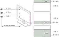
如图1所示,利用眼镜型方法的图像显示装置可以在显示板3上包括经构图的延迟器5,用于转换入射在偏振眼镜6上的光的偏振特性。在眼镜型方法中,在显示板3上交替地显示左眼图像(L)和右眼图像(R),并且通过经构图的延迟器5来转换入射在偏振眼镜6上的光的偏振特性。通过这种操作,眼镜型方法通过空间地分割左眼图像(L)和右眼图像(R)来实现3D图像。在图1中,标号1表示向显示板3提供光的背光单元,标号2和标号4表示分别粘接到显示板3的上表面和下表面以选择线偏振的偏振片。As shown in FIG. 1 , an image display device using a glasses-type method may include a patterned
在眼镜型方法中,3D图像的可视性由于在向上或向下视角的位置处产生的串扰而劣化。结果,在一般的眼镜型方法中,能够允许用户观看图像质量不错的3D图像的向上/向下视角非常窄。串扰的产生是由于在向上/向下视角处左眼图像(L)穿过右眼的经构图的延迟器区域和左眼的经构图的延迟器区域,而右眼图像(R)穿过左眼的经构图的延迟器区域和右眼的经构图的延迟器区域。因而,如图2所示,日本特开No.2002-185983公开了一种通过在与显示板的黑底(BM)相对应的经构图的延迟器区域中形成黑色条纹(BS)而获得更宽的向上/向下视角以改善3D图像的可视性的方法。在图2中,当在预定距离(D)进行观察时,理论上不产生串扰的视角(α)取决于显示板的黑底(BM)的尺寸、经构图的延迟器的黑色条纹(BS)的尺寸以及显示板与经构图的延迟器之间的间隔体。随着黑底的尺寸和黑色条纹的尺寸增大以及显示板与经构图的延迟器之间的间隔体减小,视角(α)变宽。In the glasses-type method, visibility of 3D images is degraded due to crosstalk generated at positions of upward or downward viewing angles. As a result, in a general glasses-type method, an upward/downward viewing angle capable of allowing a user to view a 3D image with good image quality is very narrow. Crosstalk occurs due to the left eye image (L) passing through the patterned retarder region of the right eye and the patterned retarder region of the left eye at up/down viewing angles, while the right eye image (R) passing through the left eye The patterned retarder area of the eye and the patterned retarder area of the right eye. Thus, as shown in FIG. 2 , Japanese Patent Laid-Open No. 2002-185983 discloses a method for obtaining a more robust pattern by forming a black stripe (BS) in a patterned retarder region corresponding to a black matrix (BM) of a display panel. A method of wide up/down viewing angles to improve the visibility of 3D images. In Fig. 2, when viewed at a predetermined distance (D), the viewing angle (α) that theoretically does not cause crosstalk depends on the size of the black matrix (BM) of the display panel, the black stripe (BS) of the patterned retarder The dimensions and the spacer between the display panel and the patterned retarder. As the size of the black matrix and the size of the black stripes increase and the spacer between the display panel and the patterned retarder decreases, the viewing angle (α) becomes wider.
但是,现有技术的图像显示装置存在以下问题。However, the conventional image display device has the following problems.
首先,经构图的延迟器的用于通过改善视角来提高3D图像的可视性的黑色条纹与显示板的黑底相互作用,从而产生了摩尔条纹(moire)。当显示2D图像时,2D图像的可视性更加劣化。图3示出了在与应用了黑色条纹的显示装置相距4米的位置处观察47英寸显示装置样品所得到的结果。当显示2D图像时,基于观察位置A、B和C分别可见90mm、150mm和355mm的摩尔条纹。First, the black stripes of the patterned retarder for improving the visibility of 3D images by improving the viewing angle interact with the black matrix of the display panel, thereby generating moire. When a 2D image is displayed, the visibility of the 2D image is further degraded. FIG. 3 shows the results obtained by observing a 47-inch display device sample at a distance of 4 meters from the display device to which the black stripes were applied. When a 2D image is displayed, moiré fringes of 90 mm, 150 mm, and 355 mm are visible based on observation positions A, B, and C, respectively.
其次,用于通过改善视角来提高3D图像的可视性的黑色条纹导致了使2D图像的亮度大幅下降的副作用。如图4(b)所示,这是由于在现有技术中,显示板的预定部分的像素被黑色条纹图案所覆盖。因此,当显示2D图像时,与图4(a)所示的不形成黑色条纹的情况相比,发光量减少了大约30%。Second, the black stripes for improving the visibility of the 3D image by improving the viewing angle cause a side effect of greatly reducing the brightness of the 2D image. As shown in FIG. 4(b), this is because, in the prior art, pixels of a predetermined portion of the display panel are covered by black stripe patterns. Therefore, when a 2D image is displayed, the amount of light emission is reduced by about 30% compared to the case where black stripes are not formed as shown in FIG. 4( a ).
发明内容Contents of the invention
本发明的示例性实施方式提供了一种能够改善2D图像和3D图像的可视性并防止显示2D图像时亮度下降的图像显示装置。Exemplary embodiments of the present invention provide an image display device capable of improving visibility of 2D images and 3D images and preventing a decrease in luminance when displaying 2D images.
一方面,本发明提供了这样一种图像显示装置,该图像显示装置包括:包括多个红色、绿色和蓝色子像素的显示板,所述显示板被设置成选择性地显示2D图像和3D图像;和位于所述显示板前面的经构图的延迟器,所述经构图的延迟器被设置成在显示所述3D图像时将来自所述显示板的光分成第一偏振的光和第二偏振的光,其中,所述多个红色、绿色和蓝色子像素中的每一个都包括主子像素和副子像素,所述主子像素包括通过数据线来接收数据电压的第一像素电极和位置与第一像素电极相对并通过公共线来接收公共电压的公共电极,所述副子像素包括通过所述数据线来接收所述数据电压的第二像素电极、位置与第二像素电极相对的公共电极,以及基于所显示的图像选择性地将第二像素电极连接到所述公共电极的放电薄膜晶体管(TFT)。In one aspect, the present invention provides an image display device comprising: a display panel comprising a plurality of red, green and blue sub-pixels, the display panel being configured to selectively display 2D images and 3D an image; and a patterned retarder positioned in front of the display panel, the patterned retarder configured to split light from the display panel into light of a first polarization and a second polarization when displaying the 3D image. polarized light, wherein each of the plurality of red, green and blue sub-pixels includes a main sub-pixel and a sub-sub-pixel, the main sub-pixel includes a first pixel electrode receiving a data voltage through a data line and a position A common electrode opposite to the first pixel electrode and receiving a common voltage through a common line, the sub-sub-pixel includes a second pixel electrode receiving the data voltage through the data line, and a common electrode opposite to the second pixel electrode. electrode, and a discharge thin film transistor (TFT) selectively connecting the second pixel electrode to the common electrode based on the displayed image.
附图说明Description of drawings
附图被包括在本说明书中以提供对本发明的进一步理解,并结合到本说明书中且构成本说明书的一部分,附图示出了本发明的实施方式,且与说明书一起用于解释本发明的原理。在附图中:The accompanying drawings, which are included in this specification to provide a further understanding of the invention, are incorporated in this specification and constitute a part of this specification, illustrate the embodiments of the present invention, and together with the specification serve to explain the concept of the present invention. principle. In the attached picture:
图1示意性地例示了眼镜型图像显示装置;FIG. 1 schematically illustrates a glasses-type image display device;
图2例示了具有现有技术的黑色条纹图案的图像显示装置;2 illustrates an image display device having a prior art black stripe pattern;
图3例示了在现有技术图像显示装置中由黑色条纹图案产生的摩尔条纹;3 illustrates moiré fringes generated by a black stripe pattern in a prior art image display device;
图4例示了现有技术图像显示装置中发光量由于黑色条纹图案的减少;FIG. 4 illustrates the reduction of the light emission amount due to the black stripe pattern in the prior art image display device;
图5是根据本发明示例性实施方式的图像显示装置的框图;5 is a block diagram of an image display device according to an exemplary embodiment of the present invention;
图6例示了单位像素的结构;FIG. 6 illustrates the structure of a unit pixel;
图7例示了子像素的第一示例性连接结构;FIG. 7 illustrates a first exemplary connection structure of sub-pixels;
图8例示了子像素的第二示例性连接结构;FIG. 8 illustrates a second exemplary connection structure of sub-pixels;
图9例示了用于操作图7和图8中示出的子像素的信号的波形和这些子像素的充电波形;FIG. 9 illustrates waveforms of signals for operating the subpixels shown in FIGS. 7 and 8 and charging waveforms of these subpixels;
图10例示了子像素的第三示例性连接结构;FIG. 10 illustrates a third exemplary connection structure of sub-pixels;
图11例示了子像素的第四示例性连接结构;FIG. 11 illustrates a fourth exemplary connection structure of sub-pixels;
图12例示了用于操作图10和图11中示出的子像素的信号的波形和这些子像素的充电波形;12 illustrates waveforms of signals for operating the subpixels shown in FIGS. 10 and 11 and charging waveforms of these subpixels;
图13例示了放电TFT的导通时段的示例性扩展;FIG. 13 illustrates an exemplary extension of the conduction period of a discharge TFT;
图14A例示了3D模式下显示在单位像素上的图像;FIG. 14A illustrates an image displayed on a unit pixel in a 3D mode;
图14B例示了2D模式下显示在单位像素上的图像;FIG. 14B illustrates an image displayed on a unit pixel in 2D mode;
图15是例示了副子像素的垂直间距与3D视角之间关系的图;FIG. 15 is a diagram illustrating a relationship between a vertical pitch of a sub-subpixel and a 3D viewing angle;
图16示意性例示了图像显示装置在3D模式下的操作;FIG. 16 schematically illustrates the operation of an image display device in a 3D mode;
图17示意性例示了图像显示装置在2D模式下的操作;FIG. 17 schematically illustrates the operation of the image display device in 2D mode;
图18是例示了基于3D视角的3D图像串扰值的图;FIG. 18 is a diagram illustrating a 3D image crosstalk value based on a 3D viewing angle;
图19是例示了根据本发明示例性实施方式的3D图像的向上视角与现有技术中的3D图像的向上视角之间的比较的图。FIG. 19 is a diagram illustrating a comparison between an upward viewing angle of a 3D image according to an exemplary embodiment of the present invention and an upward viewing angle of a 3D image in the related art.
具体实施方式Detailed ways
下面将详细描述本发明的实施方式,在附图中例示了其示例。Reference will now be made in detail to embodiments of the invention, examples of which are illustrated in the accompanying drawings.
图5是根据本发明示例性实施方式的图像显示装置的框图。图6例示了该图像显示装置的单位像素的结构。FIG. 5 is a block diagram of an image display device according to an exemplary embodiment of the present invention. FIG. 6 illustrates the structure of a unit pixel of the image display device.
如图5所示,根据本发明示例性实施方式的图像显示装置包括显示部件11、控制器12、板驱动电路14、经构图的延迟器18以及偏振眼镜20。经构图的延迟器18与偏振眼镜20充当3D驱动部件并通过空间地分离左眼图像和右眼图像来实现双眼相差。As shown in FIG. 5 , an image display device according to an exemplary embodiment of the present invention includes a
显示部件11可以被实现为液晶显示部件。液晶显示部件包括液晶显示板10、位于液晶显示板10下方的背光单元17、位于液晶显示板10与经构图的延迟器18之间的上偏振膜16a以及位于液晶显示板10与背光单元17之间的下偏振膜16b。The
液晶显示板10包括上玻璃基板、下玻璃基板以及插入在上玻璃基板与下玻璃基板之间的液晶层。薄膜晶体管(TFT)阵列形成在下玻璃基板上。TFT阵列包括被供应R(红色)、G(绿色)和B(蓝色)数据电压的多条数据线、与数据线交叉并接收选通脉冲(或扫描脉冲)的多条选通线、形成在数据线与选通线的交叉处的多个TFT、用于向液晶单元充入数据电压的多个像素电极、连接到各个像素电极并保持液晶单元的电压的存储电容器。滤色器阵列形成在上玻璃基板上。该滤色器阵列包括黑底和滤色器等。位置与像素电极相对并与像素电极一起形成电场的公共电极在如扭曲向列(TN)模式和垂直对准(VA)模式的垂直电场驱动模式下形成在上玻璃基板上。在诸如面内切换(IPS)模式或边缘场切换(FFS)模式的水平电场驱动模式下,公共电极可以与像素电极一起形成在下玻璃基板上。按照透射率或灰度级随着数据电压与供应给公共电极的公共电压之间的差异增大而提高的常黑(normally black)模式来驱动液晶单元。上偏振膜16a粘接在上玻璃基板上,下偏振膜16b粘接在下玻璃基板上。上玻璃基板和下玻璃基板中与液晶相接触的内表面上分别形成有用于设置液晶的预倾角的配向层。列间隔体可以形成在上玻璃基板与下玻璃基板之间以保持液晶单元的单元间隙不变。The liquid
如图6所示,形成在液晶显示板10上的单位像素P包括R子像素SPr、G子像素SPg和B子像素SPb。R子像素SPr包括位于选通线GLj的相对侧的R主子像素SPr1和R副子像素SPr2。当选通线GLj被激活时,R主子像素SPr1和R副子像素SPr2电连接到第一数据线DLj。G子像素SPg包括位于选通线GLj的相对侧的G主子像素SPg1和G副子像素SPg2。当选通线GLj被激活时,G主子像素SPg1和G副子像素SPg2电连接到第二数据线DL(j+1)。B子像素SPg包括位于选通线GLj的相对侧的B主子像素SPb1和B副子像素SPb2。当选通线GLj被激活时,B主子像素SPb1和B副子像素SPb2电连接到第三数据线DL(j+2)。参照图7到图15来详细描述R、G和B子像素的连接结构和操作效果。As shown in FIG. 6, the unit pixel P formed on the liquid
板驱动电路14包括用于驱动液晶显示板10的数据线的数据驱动电路和用于驱动液晶显示板10的选通线的选通驱动电路。数据驱动电路在控制器12的控制下将2D或3D数据格式的RGB数字视频数据转换成模拟伽马电压以生成R、G和B数据电压。数据驱动电路接着将R、G和B数据电压供应给数据线。选通驱动电路在控制器12的控制下生成扫描脉冲并利用扫描脉冲来依次激活选通线。The
控制器12响应于通过用户接口(未示出)输入的模式选择信号或从输入的图像信号中提取出的2D/3D识别码,在2D模式Mode_2D或3D模式Mode_3D下控制板驱动电路14。如图9所示,控制器12可以改变控制电压Vct的电平,使得控制TFTCT基于2D/3D模式而导通或截止。例如,控制器12在3D模式Mode_3D下生成具有第一电平L1的控制电压Vct,使得控制TFT CT可以导通。控制器12在2D模式Mode_2D下生成具有第二电平L2的控制电压Vct,使得控制TFT CT可以截止。The
此外,如图12所示,控制器12可以基于2D/3D模式相等地或有差别地在3D模式Mode_3D下生成施加到第一控制线VL1和第二控制线VL2的电压。例如,在3D模式Mode_3D下,控制器12可以生成将被施加到第一控制线VL1的具有第一电平Vdd的电源和将被施加到第二控制线VL2的具有比第一电平Vdd低的第二电平Vss的电压。在2D模式Mode_2D下,控制器12可以生成将被施加到第一和第二控制线VL1和VL2的具有第二电平Vss的电压。In addition, as shown in FIG. 12 , the
在3D模式Mode_3D下,控制器12将从视频源输入的3D数据格式的RGB数字视频数据分离成与液晶显示板10的分辨率一致的3D数据格式的左眼RGB数据(以下称为“左眼数据”)和3D数据格式的右眼RGB数据(以下称为“右眼数据”)。控制器12接着向数据驱动电路交替地供应与一条水平线相对应的左眼数据和与一条水平线相对应的右眼数据。数据分离操作可以由外部系统板来执行。在2D模式Mode_2D下,控制器12与液晶显示板10的分辨率相一致地布置从视频源输入的2D数据格式的RGB数字视频数据,并且向数据驱动电路提供所布置的2D数据格式的RGB数字视频数据。In the 3D mode Mode_3D, the
控制器12利用从系统板接收到的诸如垂直同步信号、水平同步信号、点时钟和数据使能信号的定时信号来产生用于控制板驱动电路14的操作定时的定时控制信号。控制器12可以将定时控制信号乘以N,并且可以按照(N×f)Hz的帧频来控制板驱动电路14的操作,其中N是大于等于2的正整数,F是输入帧频。The
背光单元17包括多个光源和多个光学部件,所述多个光学部件将来自光源的光转换成来自表面光源的光并且将来自表面光源的光照射到液晶显示板10。光源可以被实现为热阴极荧光灯(HCFL)、冷阴极荧光灯(CCFL)、外部电极荧光灯(EEFL)、发光二极管(LED)中的一种或两种或更多种。光学部件包括导光板(或扩散片)、棱镜片、散射片等,提高了来自光源的光的均匀性。The backlight unit 17 includes a plurality of light sources and a plurality of optical components that convert light from the light sources into light from the surface light source and irradiate the light from the surface light source to the liquid
经构图的延迟器18可以被经构图在玻璃基板、透明塑料基板和薄膜中的一种上。上面形成有经构图的延迟器18的基板等利用粘接剂粘接到上偏振膜16a上。经构图的延迟器18包括光吸收轴彼此垂直的第一和第二延迟器,并且将3D图像分离成偏振分量。第一延迟器形成在经构图的延迟器18的奇数行上并且透射通过上偏振膜16a而入射的光的第一偏振(例如,圆偏振或线偏振)分量。第二延迟器形成在经构图的延迟器18的偶数行上并且透射通过上偏振膜16a而入射的光的第二偏振(例如,圆偏振或线偏振)分量。例如,第一延迟器可以被实现为透射左旋圆偏振光的偏振滤波器,第二延迟器可以被实现为透射右旋圆偏振光的偏振滤波器。The patterned
偏振眼镜20被实现为,其光吸收轴根据从经构图的延迟器18输出的偏振分量而不同。例如,偏振眼镜20的左镜片透射从经构图的延迟器18的第一延迟器入射的左旋圆偏振光并阻断其它偏振分量的光,而偏振眼镜20的右镜片透射从经构图的延迟器18的第二延迟器入射的右旋圆偏振光并阻断其它偏振分量的光。在此情况下,偏振眼镜20的左镜片可以包括左旋圆偏振滤波器,偏振眼镜20的右镜片可以包括右旋圆偏振滤波器。The
图7到图15例示了子像素的连接结构和操作效果。在图7到图10中,子像素对应于R子像素、G子像素和B子像素中的每一个。7 to 15 illustrate connection structures and operational effects of sub-pixels. In FIGS. 7 to 10 , a sub-pixel corresponds to each of an R sub-pixel, a G sub-pixel, and a B sub-pixel.
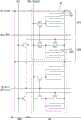
如图7和图8所示,子像素SP包括位于第k条选通线GLk的相对侧的主子像素SP1和副子像素,其中k是正整数。As shown in FIGS. 7 and 8 , the sub-pixel SP includes a main sub-pixel SP1 and a sub-sub-pixel located on opposite sides of the k-th gate line GLk, where k is a positive integer.
如图7所示,主子像素SP1包括彼此相对设置的第一像素电极Ep1和公共电极Ec。第一像素电极Ep1通过第一TFT ST1选择性地连接到第k条数据线DLk。第一TFT ST1响应于第k个扫描脉冲SPk而导通,并且将第k条数据线DLk上的数据电压Vdata供应给第一像素电极Ep1。为此,第一TFT ST1的栅极连接到第k条选通线GLk,第一TFT ST1的源极连接到第k条数据线DLk,并且第一TFT ST1的漏极连接到第一像素电极Ep1。公共电极Ec连接到被充入了公共电压Vcom的公共线。As shown in FIG. 7 , the main sub-pixel SP1 includes a first pixel electrode Ep1 and a common electrode Ec disposed opposite to each other. The first pixel electrode Ep1 is selectively connected to the k-th data line DLk through the first TFT ST1. The first TFT ST1 is turned on in response to the kth scan pulse SPk, and supplies the data voltage Vdata on the kth data line DLk to the first pixel electrode Ep1. For this, the gate of the first TFT ST1 is connected to the kth gate line GLk, the source of the first TFT ST1 is connected to the kth data line DLk, and the drain of the first TFT ST1 is connected to the first pixel electrode Ep1. The common electrode Ec is connected to a common line charged with a common voltage Vcom.
副子像素SP2包括彼此相对设置的第二像素电极Ep2和公共电极Ec,以及基于驱动模式(即,2D/3D模式)选择性地将第二像素电极Ep2连接到公共电极Ec的放电TFT DST。第二像素电极Ep2通过第二TFT ST2选择性地连接到第一像素电极Ep1。第二TFT ST2响应于第k个扫描脉冲而导通,由此将第一像素电极Ep1上的数据电压Vdata供应给第二像素电极Ep2。为此,第二TFT ST2的栅极连接到第k条选通线GLk,第二TFT ST2的源极连接到第一像素电极Ep1,并且第二TFT ST2的漏极连接到第二像素电极Ep2。放电TFT DST响应于通过控制TFT CT施加的第(k+1)个扫描脉冲而导通,因而将第二像素电极Ep2上的数据电压Vdata放电到公共电压Vcom的电平。为此,放电TFT DST的栅极通过TFT CT连接到第(k+1)条选通线GL(k+1),放电TFT DST的源极连接到第二像素电极Ep2,放电TFT DST的漏极连接到公共电极Ec。The sub-subpixel SP2 includes a second pixel electrode Ep2 and a common electrode Ec disposed opposite to each other, and a discharge TFT DST selectively connecting the second pixel electrode Ep2 to the common electrode Ec based on a driving mode (ie, 2D/3D mode). The second pixel electrode Ep2 is selectively connected to the first pixel electrode Ep1 through the second TFT ST2. The second TFT ST2 is turned on in response to the kth scan pulse, thereby supplying the data voltage Vdata on the first pixel electrode Ep1 to the second pixel electrode Ep2. For this, the gate of the second TFT ST2 is connected to the kth gate line GLk, the source of the second TFT ST2 is connected to the first pixel electrode Ep1, and the drain of the second TFT ST2 is connected to the second pixel electrode Ep2 . The discharge TFT DST is turned on in response to the (k+1)th scan pulse applied through the control TFT CT, thereby discharging the data voltage Vdata on the second pixel electrode Ep2 to the level of the common voltage Vcom. To this end, the gate of the discharge TFT DST is connected to the (k+1) gate line GL(k+1) through the TFT CT, the source of the discharge TFT DST is connected to the second pixel electrode Ep2, and the drain of the discharge TFT DST pole is connected to the common electrode Ec.
基于从控制器12接收到的控制电压Vct来对控制TFT CT的用于切换第(k+1)条选通线GL(k+1)与放电TFT DST的栅极之间的电流路径的切换操作进行控制。控制TFT CT可以设置在液晶显示板10的不显示图像的非显示区域NAA中。在图7中,“AA”表示液晶显示板10的包括子像素并显示图像的显示区域AA。The switching of the current path for switching the (k+1)th gate line GL(k+1) of the control TFT CT between the gate line GL(k+1) and the gate of the discharge TFT DST is controlled based on the control voltage Vct received from the
图8的第二TFT ST2的连接结构与图7不同。如图8所示,第二像素电极Ep2通过第二TFT ST2连接到第k条数据线DLk。第二TFT ST2响应于第k个扫描脉冲SPk而导通,因而将第k条数据线DLk上的数据电压Vdata供应给第二像素电极Ep2。为此,第二TFT ST2的栅极连接到第k条选通线GLk,第二TFT ST2的源极连接到第k条数据线DLk,第二TFT ST2的漏极连接到第二像素电极Ep2。The connection structure of the second TFT ST2 of FIG. 8 is different from that of FIG. 7 . As shown in FIG. 8, the second pixel electrode Ep2 is connected to the k-th data line DLk through the second TFT ST2. The second TFT ST2 is turned on in response to the kth scan pulse SPk, thereby supplying the data voltage Vdata on the kth data line DLk to the second pixel electrode Ep2. To this end, the gate of the second TFT ST2 is connected to the kth gate line GLk, the source of the second TFT ST2 is connected to the kth data line DLk, and the drain of the second TFT ST2 is connected to the second pixel electrode Ep2 .
下面,基于图7和图8中例示的连接结构和图9中例示的信号波形与充电波形,根据驱动模式(2D/3D模式)来描述子像素SP的操作和效果。Next, based on the connection structures illustrated in FIGS. 7 and 8 and the signal waveform and charging waveform illustrated in FIG. 9 , the operation and effect of the sub-pixel SP will be described according to the driving mode (2D/3D mode).
在3D模式Mode_3D下,控制TFT CT响应于具有第一电平L1的控制电压Vct而持续地保持导通状态。In the 3D mode Mode_3D, the control TFT CT is continuously maintained in an on state in response to the control voltage Vct having the first level L1.
在输入第k个扫描脉冲SPk的时段T1中,第一TFT ST1和第二TFT ST2导通。因此,向主子像素SP1的第一像素电极Ep1和副子像素SP2的第二像素电极Ep2施加了相同的数据电压Vdata。在时段T1中,由于放电TFT DST保持在截止状态,因此向主子像素SP1充入了跟第一像素电极Ep1与公共电极Ec之间的电压差(即,Vdata-Vcom或Vcom-Vdata)相对应的第一像素电压Vpu,并且向副子像素SP2充入了跟第二像素电极Ep2与公共电极Ec之间的电压差(即,Vdata-Vcom或Vcom-Vdata)相对应的第二像素电压Vpd。在此情况下,第一像素电压Vpu与第二像素电压Vpd具有相同的电平。In the period T1 in which the k-th scan pulse SPk is input, the first TFT ST1 and the second TFT ST2 are turned on. Therefore, the same data voltage Vdata is applied to the first pixel electrode Ep1 of the main sub-pixel SP1 and the second pixel electrode Ep2 of the sub-sub-pixel SP2. In the period T1, since the discharge TFT DST is kept in the off state, the main sub-pixel SP1 is charged with the voltage corresponding to the voltage difference between the first pixel electrode Ep1 and the common electrode Ec (that is, Vdata-Vcom or Vcom-Vdata). The second pixel voltage Vpd corresponding to the voltage difference between the second pixel electrode Ep2 and the common electrode Ec (that is, Vdata-Vcom or Vcom-Vdata) is charged to the sub-subpixel SP2 . In this case, the first pixel voltage Vpu and the second pixel voltage Vpd have the same level.
在输入第(k+1)个扫描脉冲SP(k+1)的时段T2中,第一TFT ST1和第二TFT ST2截止,而放电TFT DST导通。因此,主子像素SP1的第一像素电压Vpu被保持在充电电平,而副子像素SP2的第二像素电压Vpd被放电到公共电压Vcom的电平。In the period T2 in which the (k+1)th scan pulse SP(k+1) is input, the first TFT ST1 and the second TFT ST2 are turned off, and the discharge TFT DST is turned on. Accordingly, the first pixel voltage Vpu of the main sub-pixel SP1 is maintained at the charging level, and the second pixel voltage Vpd of the sub-sub-pixel SP2 is discharged to the level of the common voltage Vcom.
在相应帧中跟随在时段T2后的时段T3中,主子像素SP1持续地将第一电压Vpu保持在充电电平。因此,如图14A所示,在主子像素SP1上显示了3D图像。副子像素SP2持续地将第二像素电压Vpd保持在公共电压Vcom的放电电平。因此,如图14A所示,在副子像素SP2上显示了黑图像。在3D模式Mode_3D下,黑图像增加了在垂直方向上彼此相邻的3D图像之间的显示间隔。因此,本发明的示例性实施方式无需单独的黑色条纹图案就能够通过黑色图像来大范围地保证3D向上或向下视角,因而与现有技术相比可以极大地提高3D可视性。In the period T3 following the period T2 in the corresponding frame, the main sub-pixel SP1 continuously maintains the first voltage Vpu at the charging level. Therefore, as shown in FIG. 14A , a 3D image is displayed on the main sub-pixel SP1. The sub-subpixel SP2 continuously maintains the second pixel voltage Vpd at the discharge level of the common voltage Vcom. Therefore, as shown in FIG. 14A, a black image is displayed on the sub sub-pixel SP2. In the 3D mode Mode_3D, the black image increases the display interval between 3D images adjacent to each other in the vertical direction. Accordingly, the exemplary embodiment of the present invention can widely secure a 3D upward or downward viewing angle through a black image without a separate black stripe pattern, and thus can greatly improve 3D visibility compared to the related art.
另一方面,在2D模式Mode_2D下,控制TFT CT响应于第二电平L2的控制电压Vct而持续地保持截止状态。因此,放电TFT DST持续地保持截止状态。On the other hand, in the 2D mode Mode_2D, the control TFT CT is continuously kept in the off state in response to the control voltage Vct of the second level L2. Therefore, the discharge TFT DST is continuously kept in an off state.
在输入第k个扫描脉冲SPk的时段T1中,由于第一TFT ST1和第二TFT ST2的导通操作,向主子像素SP1的第一像素电极Ep1和副子像素SP2的第二像素电极Ep2施加了相同的数据电压Vdata。在时段T1中,向主子像素SP1充入了跟第一像素电极Ep1与公共电极Ec之间的电压差(即,Vdata-Vcom或Vcom-Vdata)相对应的第一像素电压Vpu,并且向副子像素SP2充入了跟第二像素电极Ep2与公共电极Ec之间的电压差(即,Vdata-Vcom或Vcom-Vdata)相对应的第二像素电压Vpd。在此情况下,第一像素电压Vpu与第二像素电压Vpd具有相同的电平。In the period T1 in which the kth scan pulse SPk is input, due to the conduction operation of the first TFT ST1 and the second TFT ST2, the first pixel electrode Ep1 of the main sub-pixel SP1 and the second pixel electrode Ep2 of the sub-sub-pixel SP2 are applied the same data voltage Vdata. In the period T1, the main sub-pixel SP1 is charged with the first pixel voltage Vpu corresponding to the voltage difference between the first pixel electrode Ep1 and the common electrode Ec (ie, Vdata-Vcom or Vcom-Vdata), and the secondary The sub-pixel SP2 is charged with the second pixel voltage Vpd corresponding to the voltage difference between the second pixel electrode Ep2 and the common electrode Ec (ie, Vdata-Vcom or Vcom-Vdata). In this case, the first pixel voltage Vpu and the second pixel voltage Vpd have the same level.
在输入第(k+1)个扫描脉冲SP(k+1)的时段T2和相应帧中跟随在时段T2后的时段T3中,由于第一TFT ST1的截止操作,主子像素SP1持续地将第一像素电压Vpu保持在充电电平。因此,如图14B所示,在主子像素SP1上显示了2D图像。另外,由于第二TFT ST2的截止操作,副子像素SP2持续地将第二像素电压Vpd保持在充电电平。因此,如图14B所示,在副子像素SP2上显示了与主子像素SP1相同的2D图像。在2D模式Mode_2D下,副子像素SP2上显示的2D图像提高了2D图像的亮度。因此,本发明的示例性实施方式可以在显示2D图像时防止亮度下降和摩尔条纹并因而可以极大地提高2D可视性。During the period T2 in which the (k+1)th scan pulse SP(k+1) is input and the period T3 following the period T2 in the corresponding frame, the main sub-pixel SP1 continuously turns the first TFT ST1 on due to the off operation of the first TFT ST1. A pixel voltage Vpu is maintained at the charging level. Therefore, as shown in FIG. 14B , a 2D image is displayed on the main sub-pixel SP1. In addition, the sub-sub-pixel SP2 continuously maintains the second pixel voltage Vpd at the charging level due to the turn-off operation of the second TFT ST2. Therefore, as shown in FIG. 14B , the same 2D image as that of the main sub-pixel SP1 is displayed on the sub-sub-pixel SP2. In the 2D mode Mode_2D, the brightness of the 2D image displayed on the sub-sub-pixel SP2 is improved. Accordingly, the exemplary embodiments of the present invention can prevent brightness drop and moiré when displaying 2D images and thus can greatly improve 2D visibility.
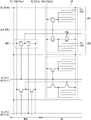
由于图7和图8中示出的控制TFT CT在3D模式Mode_3D下持续地导通,因此控制TFT CT可能由于选通偏压而很容易劣化。为了对此做出补偿,可以使用图10和图11中示出的复用(mux)开关电路MST来替换图7和图8中示出的控制TFT CT。由于图10和图11中示出的子像素在结构上大体与图7和图8中示出的子像素相同,因此可以简要地作进一步描述或者可以完全省略进一步描述。Since the control TFT CT shown in FIGS. 7 and 8 is continuously turned on in the 3D mode Mode_3D, the control TFT CT may be easily degraded due to gate bias. To compensate for this, the control TFT CT shown in FIGS. 7 and 8 may be replaced with a multiplexing (mux) switch circuit MST shown in FIGS. 10 and 11 . Since the sub-pixels shown in FIGS. 10 and 11 are substantially the same in structure as the sub-pixels shown in FIGS. 7 and 8 , further description may be briefly made or may be omitted entirely.
如图10和图11所示,复用开关电路MST响应于第(k+1)个扫描脉冲SP(k+1)来对第一控制线VL1与放电TFT DST的栅极之间的电流路径进行开关,以将第一控制线VL1上的电压施加到放电TFT DST的栅极。此外,复用开关电路MST响应于第(k+2)个扫描脉冲之后的一个扫描脉冲来对第二控制线VL2与放电TFT DST的栅极之间的电流路径进行开关,以将第二控制线VL2上的电压施加到放电TFT DST的栅极。As shown in FIGS. 10 and 11, the multiplexing switch circuit MST controls the current path between the first control line VL1 and the gate of the discharge TFT DST in response to the (k+1) scan pulse SP(k+1). Switching is performed to apply the voltage on the first control line VL1 to the gate of the discharge TFT DST. In addition, the multiplexing switch circuit MST switches the current path between the second control line VL2 and the gate of the discharge TFT DST in response to one scan pulse after the (k+2)th scan pulse to switch the second control line VL2 to the gate of the discharge TFT DST. The voltage on line VL2 is applied to the gate of the discharge TFT DST.
复用开关电路MST包括第一控制TFT CT1和第二控制TFT CT2。第一控制TFTCT1的栅极连接到第(k+1)条选通线GL(k+1),第一控制TFT CT1的源极连接到第一控制线VL1,第一控制TFT CT1的漏极连接到放电TFT DST的栅极。第二控制TFT CT2的栅极连接到第(k+2)条选通线GL(k+2),第二控制TFT CT2的源极连接到第二控制线VL2,第二控制TFT CT2的漏极连接到放电TFT DST的栅极。第一和第二控制线VL1和VL2与复用开关电路MST可以形成在液晶显示板10的不显示图像的非显示区域NAA中。在图10和图11中,“AA”表示液晶显示板10的包括子像素并显示图像的显示区域AA。The multiplexing switch circuit MST includes a first control TFT CT1 and a second control TFT CT2. The gate of the first control TFTCT1 is connected to the (k+1) gate line GL(k+1), the source of the first control TFT CT1 is connected to the first control line VL1, and the drain of the first control TFT CT1 Connect to the gate of the discharge TFT DST. The gate of the second control TFT CT2 is connected to the (k+2) gate line GL(k+2), the source of the second control TFT CT2 is connected to the second control line VL2, and the drain of the second control TFT CT2 The pole is connected to the gate of the discharge TFT DST. The first and second control lines VL1 and VL2 and the multiplexing switch circuit MST may be formed in the non-display area NAA of the liquid
下面,基于图10和图11中例示的连接结构和图12中例示的信号波形与充电波形,根据驱动模式(2D/3D模式)来描述子像素SP的操作和效果。Next, based on the connection structures illustrated in FIGS. 10 and 11 and the signal waveforms and charging waveforms illustrated in FIG. 12 , operations and effects of the sub-pixel SP are described according to drive modes (2D/3D modes).
在3D模式Mode_3D下,将第一电平Vdd的电压施加到第一控制线VL1,并且将第二电平Vss的电压施加到第二控制线VL2。复用开关电路MST在时段T1和T3中输出第二电平Vss的控制电压VGg,并且在时段T2中输出第一电平的控制电压VNg。In the 3D mode Mode_3D, the voltage of the first level Vdd is applied to the first control line VL1, and the voltage of the second level Vss is applied to the second control line VL2. The multiplexing switch circuit MST outputs the control voltage VGg of the second level Vss in the periods T1 and T3, and outputs the control voltage VNg of the first level in the period T2.
在输入第k个扫描脉冲SPk的时段T1中,第一TFT ST1和第二TFT ST2导通。因此,向主子像素SP1的第一像素电极Ep1和副子像素SP2的第二像素电极Ep2施加了相同的数据电压Vdata。在时段T1中,由于放电TFT DST响应于第二电平Vss的控制电压VNg而保持截止状态,因此向主子像素SP1充入了跟第一像素电极Ep1与公共电极Ec之间的电压差(即,Vdata-Vcom或Vcom-Vdata)相对应的第一像素电压Vpu,并且向副子像素SP2充入了跟第二像素电极Ep2与公共电极Ec之间的电压差(即,Vdata-Vcom或Vcom-Vdata)相对应的第二像素电压Vpd。在此情况下,第一像素电压Vpu与第二像素电压Vpd具有相同的电平。In the period T1 in which the k-th scan pulse SPk is input, the first TFT ST1 and the second TFT ST2 are turned on. Therefore, the same data voltage Vdata is applied to the first pixel electrode Ep1 of the main sub-pixel SP1 and the second pixel electrode Ep2 of the sub-sub-pixel SP2. In the period T1, since the discharge TFT DST remains in the off state in response to the control voltage VNg of the second level Vss, the main sub-pixel SP1 is charged with the voltage difference between the first pixel electrode Ep1 and the common electrode Ec (i.e. , Vdata-Vcom or Vcom-Vdata) corresponding to the first pixel voltage Vpu, and the sub-subpixel SP2 is charged with the voltage difference between the second pixel electrode Ep2 and the common electrode Ec (that is, Vdata-Vcom or Vcom -Vdata) corresponding to the second pixel voltage Vpd. In this case, the first pixel voltage Vpu and the second pixel voltage Vpd have the same level.
在输入第(k+1)个扫描脉冲SP(k+1)的时段T2中,第一TFT ST1和第二TFT ST2截止,而放电TFT DST响应于第一电平Vdd的控制电压VNg而导通。因此,主子像素SP1的第一像素电压Vpu被保持在充电电平,而副子像素SP2的第二像素电压Vpd被放电到公共电压Vcom的电平。In the period T2 in which the (k+1)th scan pulse SP(k+1) is input, the first TFT ST1 and the second TFT ST2 are turned off, and the discharge TFT DST is turned on in response to the control voltage VNg of the first level Vdd. Pass. Accordingly, the first pixel voltage Vpu of the main sub-pixel SP1 is maintained at the charging level, and the second pixel voltage Vpd of the sub-sub-pixel SP2 is discharged to the level of the common voltage Vcom.
在相应帧中跟在时段T2后的时段T3中,主子像素SP1持续地将第一电压Vpu保持在充电电平。因此,如图14A所示,在主子像素SP1上显示了3D图像。副子像素SP2持续地将第二像素电压Vpd保持在公共电压Vcom的放电电平。因此,如图14A所示,在副子像素SP2上显示了黑图像。在3D模式Mode_3D下,黑图像增加了在垂直方向上彼此相邻的3D图像之间的显示间隔。因此,本发明的示例性实施方式无需单独的黑色条纹图案就能够通过黑色图像来大范围地保证3D向上或向下视角,因而与现有技术相比可以极大地提高3D可视性。In the period T3 following the period T2 in the corresponding frame, the main sub-pixel SP1 continuously maintains the first voltage Vpu at the charging level. Therefore, as shown in FIG. 14A , a 3D image is displayed on the main sub-pixel SP1. The sub-subpixel SP2 continuously maintains the second pixel voltage Vpd at the discharge level of the common voltage Vcom. Therefore, as shown in FIG. 14A, a black image is displayed on the sub sub-pixel SP2. In the 3D mode Mode_3D, the black image increases the display interval between 3D images adjacent to each other in the vertical direction. Accordingly, the exemplary embodiment of the present invention can widely secure a 3D upward or downward viewing angle through a black image without a separate black stripe pattern, and thus can greatly improve 3D visibility compared to the related art.
在时段T3中,放电TFT DST响应于第二电平Vss的控制电压VNg而截止。放电TFT DST响应于第一电平Vdd的控制电压VNg而导通的持续时间可以设置成图12中示出的一个水平时段1H。此外,如图13所示,放电TFTDST响应于第一电平Vdd的控制电压VNg而导通的持续时间可以设置成比一个水平时段1H长的j个水平时段jH,其中j是大于1的正整数。第二控制TFT CT2的栅极必须连接到第(k+1+j)条选通线GL(k+1+j),以将第一电平Vdd的控制电压VNg的保持长度扩展到j个水平时段jH。In the period T3, the discharge TFT DST is turned off in response to the control voltage VNg of the second level Vss. The duration for which the discharge TFT DST is turned on in response to the control voltage VNg of the first level Vdd may be set to one
另一方面,在2D模式Mode_2D下,将第二电平Vss的电压施加到第一和第二控制线VL1和VL2。复用开关电路MST在时段T1到时段T3中持续地输出第二电平Vss的控制电压VNg。因此,放电TFT DST持续地保持截止状态。On the other hand, in the 2D mode Mode_2D, the voltage of the second level Vss is applied to the first and second control lines VL1 and VL2. The multiplexing switch circuit MST continuously outputs the control voltage VNg of the second level Vss in the period T1 to the period T3. Therefore, the discharge TFT DST is continuously kept in an off state.
在输入第k个扫描脉冲SPk的时段T1中,由于第一TFT ST1和第二TFT ST2的导通操作,向主子像素SP1的第一像素电极Ep1和副子像素SP2的第二像素电极Ep2施加了相同的数据电压Vdata。在时段T1中,向主子像素SP1充入跟第一像素电极Ep1与公共电极Ec之间的电压差(即,Vdata-Vcom或Vcom-Vdata)相对应的第一像素电压Vpu,并且向副子像素SP2充入跟第二像素电极Ep2与公共电极Ec之间的电压差(即,Vdata-Vcom或Vcom-Vdata)相对应的第二像素电压Vpd。在此情况下,第一像素电压Vpu与第二像素电压Vpd具有相同的电平。In the period T1 in which the kth scan pulse SPk is input, due to the conduction operation of the first TFT ST1 and the second TFT ST2, the first pixel electrode Ep1 of the main sub-pixel SP1 and the second pixel electrode Ep2 of the sub-sub-pixel SP2 are applied the same data voltage Vdata. In the period T1, the first pixel voltage Vpu corresponding to the voltage difference between the first pixel electrode Ep1 and the common electrode Ec (that is, Vdata-Vcom or Vcom-Vdata) is charged to the main sub-pixel SP1, and the sub-subpixel The pixel SP2 is charged with the second pixel voltage Vpd corresponding to the voltage difference (ie, Vdata-Vcom or Vcom-Vdata) between the second pixel electrode Ep2 and the common electrode Ec. In this case, the first pixel voltage Vpu and the second pixel voltage Vpd have the same level.
在输入第(k+1)个扫描脉冲SP(k+1)的时段T2和相应帧中跟在时段T2后的时段T3中,由于第一TFT ST1和第二TFT ST2的截止操作,主子像素SP1持续地将第一像素电压Vpu保持在充电电平。因此,如图14B所示,在主子像素SP1上显示了2D图像。另外,由于第一TFT ST1和第二TFT ST2的截止操作,副子像素SP2持续地将第二像素电压Vpd保持在充电电平。因此,如图14B所示,在副子像素SP2上显示了与主子像素SP1相同的2D图像。在2D模式Mode_2D下,副子像素SP2上显示的2D图像提高了2D图像的亮度。因此,本发明的示例性实施方式可以在显示2D图像时防止亮度下降和摩尔条纹并因而可以极大地提高2D可视性。In the period T2 in which the (k+1)th scan pulse SP(k+1) is input and the period T3 following the period T2 in the corresponding frame, due to the off-operation of the first TFT ST1 and the second TFT ST2, the main sub-pixel SP1 continuously maintains the first pixel voltage Vpu at the charging level. Therefore, as shown in FIG. 14B , a 2D image is displayed on the main sub-pixel SP1. In addition, the sub-sub-pixel SP2 continuously maintains the second pixel voltage Vpd at the charging level due to the turn-off operation of the first TFT ST1 and the second TFT ST2. Therefore, as shown in FIG. 14B , the same 2D image as that of the main sub-pixel SP1 is displayed on the sub-sub-pixel SP2. In the 2D mode Mode_2D, the brightness of the 2D image displayed on the sub-sub-pixel SP2 is improved. Accordingly, the exemplary embodiments of the present invention can prevent brightness drop and moiré when displaying 2D images and thus can greatly improve 2D visibility.
如图15所示,副子像素SP2的垂直间距与3D向上/向下视角有着紧密的关联。换言之,3D向上/向下视角随着副子像素SP2的垂直间距P2占子像素SP的垂直间距P1的百分比(P2*100)/P1的增加而增大,并且随着百分比(P2*100)/P1的减小而减小。另一方面,3D图像的亮度随着百分比(P2*100)/P1的增加而增加,并且随着百分比(P2*100)/P1的减小而减小。根据实验,当副子像素SP2的垂直间距P2与主子像素SP1的垂直间距的比是1∶2时,3D向上/向下视角与3D图像的亮度可以接近令人满意的水平。但是,由于该比可能根据3D特性而变化,因此可以考虑3D向上/向下视角与3D图像的亮度之间的关系而将副子像素SP2的垂直间距设计成适合的尺寸。As shown in FIG. 15 , the vertical pitch of the sub-sub-pixel SP2 is closely related to the 3D up/down viewing angle. In other words, the 3D upward/downward viewing angle increases as the percentage (P2*100)/P1 of the vertical pitch P2 of the sub-sub-pixel SP2 to the vertical pitch P1 of the sub-pixel SP increases, and increases as the percentage (P2*100) /P1 decreases. On the other hand, the brightness of the 3D image increases as the percentage (P2*100)/P1 increases, and decreases as the percentage (P2*100)/P1 decreases. According to experiments, when the ratio of the vertical pitch P2 of the sub-sub-pixel SP2 to the vertical pitch of the main sub-pixel SP1 is 1:2, the 3D up/down viewing angle and the brightness of the 3D image can approach a satisfactory level. However, since the ratio may vary according to 3D characteristics, the vertical pitch of the sub-sub-pixel SP2 may be designed to an appropriate size in consideration of the relationship between the 3D up/down viewing angle and the brightness of the 3D image.
图16示意性例示了图像显示装置在3D模式下的操作。FIG. 16 schematically illustrates the operation of the image display device in 3D mode.
如图16所示,在3D模式(Mode_3D)下,在位于液晶显示板10的奇数水平线上的主子像素上显示左眼RGB图像L,并且在位于液晶显示板10的偶数水平线上的主子像素上显示右眼RGB图像R。通过经构图的延迟器18的交替形成在经构图的延迟器18的一条水平线上的第一延迟器和第二延迟器,将左眼RGB图像L与右眼RGB图像R分离成偏振分量。经第一延迟器透射的左眼RGB图像L被发送到偏振眼镜20的左镜片,经第二延迟器透射的右眼RGB图像R被发送到偏振眼镜20的右镜片。因此实现了3D图像。As shown in FIG. 16 , in the 3D mode (Mode_3D), the left-eye RGB image L is displayed on the main sub-pixels located on the odd horizontal lines of the liquid
在3D模式(Mode_3D)下,在液晶显示板10的副子像素上显示黑色图像。该黑色图像提高了在垂直方向上彼此相邻的左眼RGB图像L和右眼TGB图像的显示间隔。In the 3D mode (Mode_3D), black images are displayed on the sub-sub-pixels of the liquid
图17示意性例示了图像显示装置在2D模式下的操作。FIG. 17 schematically illustrates the operation of the image display device in 2D mode.
如图17所示,在2D模式Mode_2D下,液晶显示板10的主子像素和副子像素上显示了相同的RGB图像。在副子像素上显示的RGB图像提高了2D图像的亮度。As shown in FIG. 17 , in the 2D mode Mode_2D, the same RGB image is displayed on the main sub-pixel and the sub-sub-pixel of the liquid
图18是例示了基于3D视角的3D图像的串扰值的图。在图18中,水平轴表示3D图像的向上(+)/向下(-)视角(单位:度),垂直轴表示3D串扰值(单位:%)。FIG. 18 is a graph illustrating crosstalk values of a 3D image based on a 3D viewing angle. In FIG. 18 , the horizontal axis represents an upward (+)/downward (−) viewing angle (unit: degree) of a 3D image, and the vertical axis represents a 3D crosstalk value (unit: %).
如上所述,在利用按照每一条水平线的方式交替地显示左眼图像和右眼图像的显示板和与显示板相距预定距离设置并按照每一条水平线的方式改变偏振特性的经构图的延迟器来显示3D图像的图像显示装置中,可以通过利用左眼延迟器只透过左眼图像且利用右眼延迟器只透过右眼图像来实现具有不错图像质量的3D图像。但是,当不是在图像显示装置的前面而是在向上/向下视角的位置来观察图像显示装置时,左眼图像可以穿过右眼延迟器以及左眼延迟器,而右眼图像可以穿过左眼延迟器以及右眼延迟器。因此,产生了3D串扰C/T。所产生的3D串扰由下面的等式1来表示:As described above, using a display panel that alternately displays images for the left eye and images for the right eye every horizontal line and a patterned retarder that is placed at a predetermined distance from the display panel and that changes polarization characteristics every horizontal line In an image display device displaying 3D images, it is possible to realize a 3D image with good image quality by using a left-eye retarder to transmit only a left-eye image and using a right-eye retarder to transmit only a right-eye image. However, when the image display device is viewed not in front of the image display device but at an upward/downward viewing angle position, the left-eye image may pass through the right-eye retarder and the left-eye retarder, and the right-eye image may pass through the Left eye retarder and right eye retarder. Therefore, 3D crosstalk C/T is generated. The resulting 3D crosstalk is expressed by
[等式1][equation 1]
在等式1中,LBlackRwhite是在左眼像素上显示黑色图像并在右眼像素上显示白色图像的图案的亮度值,LWhiteRBlack是在左眼像素上显示白色图像并在右眼像素上显示黑色图像的图案的亮度值,并且Black是在所有像素上显示了黑色图像后测出的亮度值。一般来讲,当通过等式1计算出的3D串扰值C/T小于等于7%时获得的视角被定义为可以得到不错图像质量的3D图像的3D视角。但是,临界值(7%)可以根据图像显示装置的型号而改变。In
如在图18的曲线中注意到的那样,用户可在3D串扰值(单位:%)小于等于预定临界值(例如,7%)的视角范围VA1内看到具有不错图像质量的3D图像。另一方面,由于左眼图像和右眼图像的交迭,用户在3D串扰值(单位:%)大于预定临界值(例如,7%)的视角范围VA2内看不到具有不错图像质量的3D图像。As noted in the graph of FIG. 18 , the user can see a 3D image with good image quality within the viewing angle range VA1 where the 3D crosstalk value (unit: %) is less than or equal to a predetermined critical value (eg, 7%). On the other hand, due to the overlapping of the left-eye image and the right-eye image, the user cannot see 3D images with good image quality within the viewing angle range VA2 where the 3D crosstalk value (unit: %) is larger than a predetermined critical value (for example, 7%). image.
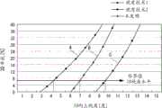
图19是例示了根据本发明示例性实施方式的3D图像的向上视角与现有技术中的3D图像的向上视角之间的比较的图。在图19中,水平轴表示3D图像的向上视角(单位:度),垂直轴表示3D图像的串扰值(单位:%)。FIG. 19 is a diagram illustrating a comparison between an upward viewing angle of a 3D image according to an exemplary embodiment of the present invention and an upward viewing angle of a 3D image in the related art. In FIG. 19 , the horizontal axis represents the upward viewing angle of the 3D image (unit: degree), and the vertical axis represents the crosstalk value of the 3D image (unit: %).
在图19中,曲线A表示左眼图像和右眼图像由于黑底而具有80μm的显示间隔而经构图的延迟器没有黑色条纹的现有技术1的向上视角。根据曲线A,在现有技术1中,满足3D串扰的临界值(例如,7%)的向上视角是大约0°到4°且非常窄。曲线C表示左眼图像和右眼图像由于黑底而具有80μm的显示间隔而经构图的延迟器具有宽度为210μm的黑色条纹图案的现有技术2的向上视角。根据曲线C,在现有技术2中,满足3D串扰的临界值(例如,7%)的向上视角是大约0°到10°并且较宽。但是,现有技术2存在2D图像的可视性和亮度由于用于保证视角的黑色条纹图案的存在而下降的副作用。In FIG. 19 , curve A represents the upward viewing angle of
相反,在显示3D图像时,本发明的示例性实施方式无需单独的黑色条纹图案就可以充分地保证左眼图像与右眼图像之间的显示间隔。因而,如图19中的曲线B所示,在不降低2D图像的可视性和亮度的情况下,满足3D串扰的临界值(例如,7%)的向上视角可以增加到大约0°到7°。In contrast, the exemplary embodiment of the present invention can sufficiently secure the display interval between the left-eye image and the right-eye image without a separate black stripe pattern when displaying a 3D image. Thus, as shown in curve B in FIG. 19 , without reducing the visibility and brightness of the 2D image, the upward viewing angle that satisfies the critical value (for example, 7%) of 3D crosstalk can be increased to about 0° to 7°. °.
如上所述,根据本发明示例性实施方式的图像显示装置可以提高2D和3D图像的可视性并且特别在显示2D图像过程中可以防止亮度下降。As described above, the image display device according to the exemplary embodiments of the present invention can improve the visibility of 2D and 3D images and can prevent a decrease in brightness particularly during displaying a 2D image.
尽管参照多个示例性实施方式描述了实施方式,应理解的是本领域技术人员可建议落入本公开的原理的精神和范围内的许多其它修改和实施方式。更具体地,在本公开、附图以及所附的权利要求的范围内,在主题组合设置的组成部分和/或设置中可以做出各种变型和修改。除了组成部分和/或设置中的变型和修改之外,替换使用对于本领域技术人员也是明显的。Although embodiments have been described with reference to a number of illustrative embodiments thereof, it should be understood that numerous other modifications and embodiments can be devised by those skilled in the art that will fall within the spirit and scope of the principles of this disclosure. More particularly, various variations and modifications may be made in the constituent parts and/or arrangements of the subject combination arrangement within the scope of the disclosure, the drawings and the appended claims. Besides variations and modifications in components and/or arrangements, alternative uses will be apparent to those skilled in the art.
本申请要求2010年3月17日提交的韩国专利申请No.10-2010-0023888的优先权,此处以引证的方式并入其全部内容,就像在此进行了完整阐述一样。This application claims priority from Korean Patent Application No. 10-2010-0023888 filed March 17, 2010, the entire contents of which are hereby incorporated by reference as if fully set forth herein.
Claims (20)
Translated fromChineseApplications Claiming Priority (4)
| Application Number | Priority Date | Filing Date | Title |
|---|---|---|---|
| KR10-2010-0023888 | 2010-03-17 | ||
| KR20100023888 | 2010-03-17 | ||
| KR10-2010-0054678 | 2010-06-10 | ||
| KR1020100054678AKR101679076B1 (en) | 2010-03-17 | 2010-06-10 | Image display device |
Publications (2)
| Publication Number | Publication Date |
|---|---|
| CN102193260A CN102193260A (en) | 2011-09-21 |
| CN102193260Btrue CN102193260B (en) | 2013-12-04 |
Family
ID=44645382
Family Applications (1)
| Application Number | Title | Priority Date | Filing Date |
|---|---|---|---|
| CN2010106014705AActiveCN102193260B (en) | 2010-03-17 | 2010-12-22 | Image display device |
Country Status (2)
| Country | Link |
|---|---|
| US (1) | US8519908B2 (en) |
| CN (1) | CN102193260B (en) |
Families Citing this family (38)
| Publication number | Priority date | Publication date | Assignee | Title |
|---|---|---|---|---|
| FR2584965B1 (en)* | 1985-07-16 | 1989-10-27 | Pele Cie | METHOD AND APPARATUS FOR POLISHING PLATES |
| TWI465769B (en)* | 2011-03-18 | 2014-12-21 | Au Optronics Corp | Three-dimensional display |
| KR101829455B1 (en)* | 2011-04-20 | 2018-03-29 | 엘지디스플레이 주식회사 | Image display device and driving method thereof |
| KR101446381B1 (en)* | 2011-07-15 | 2014-10-02 | 엘지디스플레이 주식회사 | Image display device |
| KR101859677B1 (en)* | 2011-07-27 | 2018-05-21 | 삼성디스플레이 주식회사 | Display device |
| KR101818251B1 (en)* | 2011-08-04 | 2018-01-15 | 엘지디스플레이 주식회사 | Stereoscopic image display |
| CN102402026B (en)* | 2011-08-31 | 2014-07-16 | 深圳市华星光电技术有限公司 | Liquid crystal display |
| KR101868611B1 (en)* | 2011-10-05 | 2018-06-20 | 엘지디스플레이 주식회사 | Stereoscopic image display |
| KR101878482B1 (en)* | 2011-10-06 | 2018-07-16 | 엘지디스플레이 주식회사 | Stereoscopic image display |
| KR101868145B1 (en)* | 2011-10-06 | 2018-06-18 | 엘지디스플레이 주식회사 | Stereoscopic image display |
| CN102650781B (en)* | 2011-10-18 | 2014-11-19 | 京东方科技集团股份有限公司 | Pixel structure for stereoscopic display and its control method |
| TWI428901B (en)* | 2011-10-20 | 2014-03-01 | Au Optronics Corp | Liquid crystal display and display driving method thereof |
| KR101818253B1 (en)* | 2011-10-21 | 2018-01-15 | 엘지디스플레이 주식회사 | Stereoscopic Image Display Device |
| KR101457746B1 (en)* | 2011-10-26 | 2014-11-04 | 엘지디스플레이 주식회사 | Stereoscopic image display |
| TWI449954B (en)* | 2011-10-28 | 2014-08-21 | Chunghwa Picture Tubes Ltd | Method, device and system for displaying three-dimensional stereo image |
| CN102654701B (en)* | 2011-11-21 | 2014-06-11 | 京东方科技集团股份有限公司 | Array substrate, display panel and display device |
| US9171520B2 (en)* | 2011-11-21 | 2015-10-27 | Boe Technology Group Co., Ltd. | Array substrate, method for controlling the same and display panel including the array substrate |
| KR20130066902A (en)* | 2011-12-13 | 2013-06-21 | 삼성디스플레이 주식회사 | Method of displaying three-dimensional stereoscopic image and an display apparatus for performing the same |
| CN102655599B (en)* | 2012-01-05 | 2015-06-10 | 京东方科技集团股份有限公司 | Image display device and image display method |
| TWI440012B (en)* | 2012-02-17 | 2014-06-01 | Chunghwa Picture Tubes Ltd | Double-layer switchable stereo liquid crystal display and operation method thereof |
| CN102651203B (en)* | 2012-02-28 | 2014-06-11 | 京东方科技集团股份有限公司 | Display equipment and driving method thereof |
| JP5990743B2 (en)* | 2012-03-09 | 2016-09-14 | 株式会社Joled | Organic EL display device and driving method thereof |
| CN102663982B (en)* | 2012-04-27 | 2015-03-11 | 深圳市华星光电技术有限公司 | Three-dimensional display device and drive method thereof |
| CN102707492B (en)* | 2012-06-14 | 2015-05-20 | 深圳市华星光电技术有限公司 | Three-dimensional image display device of patterned phase delay |
| US9217877B2 (en) | 2012-06-14 | 2015-12-22 | Shenzhen China Star Optoelectronics Technology Co., Ltd. | Stereoscopic image display apparatus having film-type patterned retarder |
| CN102749768B (en)* | 2012-07-05 | 2015-02-25 | 深圳市华星光电技术有限公司 | 3D (Three-dimensional) display and pixel structure thereof |
| TWI489175B (en)* | 2012-11-30 | 2015-06-21 | Au Optronics Corp | Array substrate of a display panel and the driving method thereof |
| CN103257495B (en)* | 2013-05-24 | 2015-11-25 | 深圳市华星光电技术有限公司 | A kind of array base palte and display panels |
| US20150022510A1 (en)* | 2013-07-19 | 2015-01-22 | Shenzhen China Star Optoelectronics Technology Co., Ltd. | Array substrate and liquid crystal panel with the same |
| CN103531143B (en)* | 2013-10-22 | 2015-12-30 | 深圳市华星光电技术有限公司 | Array base palte and 3D display device |
| CN103728751B (en)* | 2013-12-27 | 2016-03-30 | 深圳市华星光电技术有限公司 | Switch the liquid crystal display of display two and three dimensions image |
| KR102144733B1 (en)* | 2013-12-30 | 2020-08-18 | 엘지디스플레이 주식회사 | Stereopsis image display device |
| CN103869485B (en)* | 2014-03-11 | 2016-02-24 | 深圳市华星光电技术有限公司 | The method of display device and display image thereof |
| CN103995407B (en)* | 2014-05-08 | 2016-08-24 | 京东方科技集团股份有限公司 | Array base palte and display floater |
| CN104238216B (en)* | 2014-09-03 | 2017-04-19 | 深圳市华星光电技术有限公司 | Pixel structure and display device |
| CN106200130A (en)* | 2016-09-07 | 2016-12-07 | 京东方科技集团股份有限公司 | 3d display device and 3d display system |
| CN108132570B (en) | 2016-12-01 | 2021-04-23 | 元太科技工业股份有限公司 | Display device and electronic paper display device |
| CN110047900B (en)* | 2019-04-26 | 2021-07-23 | 武汉华星光电半导体显示技术有限公司 | Display panel and electronic device |
Citations (3)
| Publication number | Priority date | Publication date | Assignee | Title |
|---|---|---|---|---|
| US5943038A (en)* | 1995-12-08 | 1999-08-24 | Kabushiki Kaisha Toshiba | Liquid crystal display panel |
| CN101093630A (en)* | 2006-06-19 | 2007-12-26 | Lg.菲利浦Lcd株式会社 | Three-dimensional image display |
| CN101196649A (en)* | 2006-12-06 | 2008-06-11 | 索尼株式会社 | Display device |
Family Cites Families (4)
| Publication number | Priority date | Publication date | Assignee | Title |
|---|---|---|---|---|
| KR101394434B1 (en)* | 2007-06-29 | 2014-05-15 | 삼성디스플레이 주식회사 | Display apparatus and driving method thereof |
| KR101381348B1 (en)* | 2008-02-14 | 2014-04-17 | 삼성디스플레이 주식회사 | Liquid crystal display |
| KR101354329B1 (en)* | 2009-04-17 | 2014-01-22 | 엘지디스플레이 주식회사 | Image display device |
| KR101318443B1 (en)* | 2009-05-29 | 2013-10-16 | 엘지디스플레이 주식회사 | Stereoscopic Image Display Device |
- 2010
- 2010-12-15USUS12/969,025patent/US8519908B2/enactiveActive
- 2010-12-22CNCN2010106014705Apatent/CN102193260B/enactiveActive
Patent Citations (3)
| Publication number | Priority date | Publication date | Assignee | Title |
|---|---|---|---|---|
| US5943038A (en)* | 1995-12-08 | 1999-08-24 | Kabushiki Kaisha Toshiba | Liquid crystal display panel |
| CN101093630A (en)* | 2006-06-19 | 2007-12-26 | Lg.菲利浦Lcd株式会社 | Three-dimensional image display |
| CN101196649A (en)* | 2006-12-06 | 2008-06-11 | 索尼株式会社 | Display device |
Also Published As
| Publication number | Publication date |
|---|---|
| US8519908B2 (en) | 2013-08-27 |
| US20110227886A1 (en) | 2011-09-22 |
| CN102193260A (en) | 2011-09-21 |
Similar Documents
| Publication | Publication Date | Title |
|---|---|---|
| CN102193260B (en) | Image display device | |
| CN101867836B (en) | Image display device | |
| CN102075775B (en) | Image display device | |
| CN102540599B (en) | Image display device and driving method thereof | |
| KR101279120B1 (en) | Image display device | |
| US9052519B2 (en) | Image display device | |
| KR101739139B1 (en) | Stereoscopic image display | |
| KR101679076B1 (en) | Image display device | |
| KR101310383B1 (en) | Stereoscopic Image Display Device | |
| US20120274748A1 (en) | Stereoscopic Image Display Device and Method for Driving the Same | |
| KR20120070986A (en) | Image display device | |
| KR101900938B1 (en) | Stereoscopic image display device | |
| KR101948894B1 (en) | Stereoscopic image display device | |
| KR101279662B1 (en) | Video display device | |
| KR101803564B1 (en) | Stereoscopic image display device and driving method thereof | |
| KR20120122606A (en) | Stereoscopic image display |
Legal Events
| Date | Code | Title | Description |
|---|---|---|---|
| C06 | Publication | ||
| PB01 | Publication | ||
| C10 | Entry into substantive examination | ||
| SE01 | Entry into force of request for substantive examination | ||
| C14 | Grant of patent or utility model | ||
| GR01 | Patent grant |