CN102187400A - Integrated circuit device - Google Patents
Integrated circuit deviceDownload PDFInfo
- Publication number
- CN102187400A CN102187400ACN2009801416666ACN200980141666ACN102187400ACN 102187400 ACN102187400 ACN 102187400ACN 2009801416666 ACN2009801416666 ACN 2009801416666ACN 200980141666 ACN200980141666 ACN 200980141666ACN 102187400 ACN102187400 ACN 102187400A
- Authority
- CN
- China
- Prior art keywords
- voltage
- integrated circuit
- output terminal
- frequency
- output
- Prior art date
- Legal status (The legal status is an assumption and is not a legal conclusion. Google has not performed a legal analysis and makes no representation as to the accuracy of the status listed.)
- Pending
Links
Images


Classifications
- G—PHYSICS
- G11—INFORMATION STORAGE
- G11C—STATIC STORES
- G11C5/00—Details of stores covered by group G11C11/00
- G11C5/02—Disposition of storage elements, e.g. in the form of a matrix array
- G11C5/04—Supports for storage elements, e.g. memory modules; Mounting or fixing of storage elements on such supports
- G—PHYSICS
- G11—INFORMATION STORAGE
- G11C—STATIC STORES
- G11C11/00—Digital stores characterised by the use of particular electric or magnetic storage elements; Storage elements therefor
- G11C11/005—Digital stores characterised by the use of particular electric or magnetic storage elements; Storage elements therefor comprising combined but independently operative RAM-ROM, RAM-PROM, RAM-EPROM cells
- G—PHYSICS
- G11—INFORMATION STORAGE
- G11C—STATIC STORES
- G11C16/00—Erasable programmable read-only memories
- G11C16/02—Erasable programmable read-only memories electrically programmable
- G11C16/06—Auxiliary circuits, e.g. for writing into memory
- G11C16/10—Programming or data input circuits
- G11C16/12—Programming voltage switching circuits
- G—PHYSICS
- G11—INFORMATION STORAGE
- G11C—STATIC STORES
- G11C16/00—Erasable programmable read-only memories
- G11C16/02—Erasable programmable read-only memories electrically programmable
- G11C16/06—Auxiliary circuits, e.g. for writing into memory
- G11C16/30—Power supply circuits
- G—PHYSICS
- G11—INFORMATION STORAGE
- G11C—STATIC STORES
- G11C5/00—Details of stores covered by group G11C11/00
- G11C5/02—Disposition of storage elements, e.g. in the form of a matrix array
- G—PHYSICS
- G11—INFORMATION STORAGE
- G11C—STATIC STORES
- G11C5/00—Details of stores covered by group G11C11/00
- G11C5/14—Power supply arrangements, e.g. power down, chip selection or deselection, layout of wirings or power grids, or multiple supply levels
- G11C5/145—Applications of charge pumps; Boosted voltage circuits; Clamp circuits therefor
- H—ELECTRICITY
- H01—ELECTRIC ELEMENTS
- H01L—SEMICONDUCTOR DEVICES NOT COVERED BY CLASS H10
- H01L25/00—Assemblies consisting of a plurality of semiconductor or other solid state devices
- H01L25/03—Assemblies consisting of a plurality of semiconductor or other solid state devices all the devices being of a type provided for in a single subclass of subclasses H10B, H10D, H10F, H10H, H10K or H10N, e.g. assemblies of rectifier diodes
- H01L25/04—Assemblies consisting of a plurality of semiconductor or other solid state devices all the devices being of a type provided for in a single subclass of subclasses H10B, H10D, H10F, H10H, H10K or H10N, e.g. assemblies of rectifier diodes the devices not having separate containers
- H01L25/065—Assemblies consisting of a plurality of semiconductor or other solid state devices all the devices being of a type provided for in a single subclass of subclasses H10B, H10D, H10F, H10H, H10K or H10N, e.g. assemblies of rectifier diodes the devices not having separate containers the devices being of a type provided for in group H10D89/00
- H01L25/0657—Stacked arrangements of devices
- H—ELECTRICITY
- H01—ELECTRIC ELEMENTS
- H01L—SEMICONDUCTOR DEVICES NOT COVERED BY CLASS H10
- H01L25/00—Assemblies consisting of a plurality of semiconductor or other solid state devices
- H01L25/18—Assemblies consisting of a plurality of semiconductor or other solid state devices the devices being of the types provided for in two or more different main groups of the same subclass of H10B, H10D, H10F, H10H, H10K or H10N
- H—ELECTRICITY
- H01—ELECTRIC ELEMENTS
- H01L—SEMICONDUCTOR DEVICES NOT COVERED BY CLASS H10
- H01L2225/00—Details relating to assemblies covered by the group H01L25/00 but not provided for in its subgroups
- H01L2225/03—All the devices being of a type provided for in the same main group of the same subclass of class H10, e.g. assemblies of rectifier diodes
- H01L2225/04—All the devices being of a type provided for in the same main group of the same subclass of class H10, e.g. assemblies of rectifier diodes the devices not having separate containers
- H01L2225/065—All the devices being of a type provided for in the same main group of the same subclass of class H10
- H01L2225/06503—Stacked arrangements of devices
- H01L2225/06513—Bump or bump-like direct electrical connections between devices, e.g. flip-chip connection, solder bumps
- H—ELECTRICITY
- H01—ELECTRIC ELEMENTS
- H01L—SEMICONDUCTOR DEVICES NOT COVERED BY CLASS H10
- H01L2225/00—Details relating to assemblies covered by the group H01L25/00 but not provided for in its subgroups
- H01L2225/03—All the devices being of a type provided for in the same main group of the same subclass of class H10, e.g. assemblies of rectifier diodes
- H01L2225/04—All the devices being of a type provided for in the same main group of the same subclass of class H10, e.g. assemblies of rectifier diodes the devices not having separate containers
- H01L2225/065—All the devices being of a type provided for in the same main group of the same subclass of class H10
- H01L2225/06503—Stacked arrangements of devices
- H01L2225/06517—Bump or bump-like direct electrical connections from device to substrate
- H—ELECTRICITY
- H01—ELECTRIC ELEMENTS
- H01L—SEMICONDUCTOR DEVICES NOT COVERED BY CLASS H10
- H01L25/00—Assemblies consisting of a plurality of semiconductor or other solid state devices
- H01L25/16—Assemblies consisting of a plurality of semiconductor or other solid state devices the devices being of types provided for in two or more different subclasses of H10B, H10D, H10F, H10H, H10K or H10N, e.g. forming hybrid circuits
- H—ELECTRICITY
- H01—ELECTRIC ELEMENTS
- H01L—SEMICONDUCTOR DEVICES NOT COVERED BY CLASS H10
- H01L2924/00—Indexing scheme for arrangements or methods for connecting or disconnecting semiconductor or solid-state bodies as covered by H01L24/00
- H01L2924/0001—Technical content checked by a classifier
- H01L2924/0002—Not covered by any one of groups H01L24/00, H01L24/00 and H01L2224/00
- H—ELECTRICITY
- H01—ELECTRIC ELEMENTS
- H01L—SEMICONDUCTOR DEVICES NOT COVERED BY CLASS H10
- H01L2924/00—Indexing scheme for arrangements or methods for connecting or disconnecting semiconductor or solid-state bodies as covered by H01L24/00
- H01L2924/19—Details of hybrid assemblies other than the semiconductor or other solid state devices to be connected
- H01L2924/191—Disposition
- H01L2924/19101—Disposition of discrete passive components
- H01L2924/19106—Disposition of discrete passive components in a mirrored arrangement on two different side of a common die mounting substrate
Landscapes
- Engineering & Computer Science (AREA)
- Microelectronics & Electronic Packaging (AREA)
- Power Engineering (AREA)
- Computer Hardware Design (AREA)
- Physics & Mathematics (AREA)
- Condensed Matter Physics & Semiconductors (AREA)
- General Physics & Mathematics (AREA)
- Dc-Dc Converters (AREA)
- Semiconductor Integrated Circuits (AREA)
Abstract
Translated fromChinese
Description
Translated fromChinese技术领域technical field
本发明涉及集成电路装置,详细地说,涉及具备由包括具有在第1电压下操作的第1集成电路的第1集成电路芯片的集成电路芯片多个层叠而成的层叠体的集成电路装置。The present invention relates to an integrated circuit device, and more specifically, relates to an integrated circuit device including a laminated body in which a plurality of integrated circuit chips including a first integrated circuit chip having a first integrated circuit operating at a first voltage are stacked.
背景技术Background technique
传统,作为该种集成电路装置,提出了具有闪速存储器的闪速存储器芯片多个层叠而成的装置(例如,参照非专利文献1)。该装置中,通过多个层叠闪速存储器芯片,实现装置的小型化。Conventionally, as such an integrated circuit device, a device including a plurality of stacked flash memory chips having a flash memory has been proposed (see, for example, Non-Patent Document 1). In this device, miniaturization of the device is realized by stacking a plurality of flash memory chips.
非专利文献1:田中啓安及另外2名,「NAND型闪速存储器」,東芝レビユ一(Toshiba Review),2008年,Vol.63,No.2,p.28-31。Non-Patent Document 1: Kean Tanaka and 2 others, "NAND Flash Memory", Toshiba Review, 2008, Vol.63, No.2, p.28-31.
发明内容Contents of the invention
闪速存储器中,用于写入存储内容用的写入电压比用于读出存储内容用的读出电压高,因此,上述集成电路装置中,需要将电源电压升压到写入电压后供给闪速存储器芯片的升压供电电路。这样的升压供电电路,即使在电源电压互异的逻辑电路和模拟电路混合搭载的模拟数字混载芯片等的集成电路芯片多个层叠而成的装置中也是必要的,虽然一般形成于集成电路芯片,但是,若在集成电路芯片形成升压供电电路,则集成电路芯片的面积变大,难以实现装置全体的小型化。In the flash memory, the write voltage for writing the stored content is higher than the read voltage for reading the stored content. Therefore, in the above-mentioned integrated circuit device, it is necessary to boost the power supply voltage to the write voltage and supply Boost power supply circuit for flash memory chips. Such a step-up power supply circuit is necessary even in a device in which a plurality of integrated circuit chips such as an analog-digital hybrid chip in which logic circuits and analog circuits with different power supply voltages are mixed are mounted. However, if the step-up power supply circuit is formed on the integrated circuit chip, the area of the integrated circuit chip will increase, making it difficult to miniaturize the entire device.
本发明的集成电路装置的主要目的是实现装置全体的小型化。The main purpose of the integrated circuit device of the present invention is to achieve miniaturization of the entire device.
本发明的集成电路装置为了达成上述的主要目的,采用以下的手段。The integrated circuit device of the present invention employs the following means in order to achieve the above-mentioned main object.
本发明的集成电路装置,其特征在于,具备:The integrated circuit device of the present invention is characterized by comprising:
层叠体,其由多个集成电路芯片层叠而成,上述集成电路芯片包括具有在第1电压下操作的第1集成电路的第1集成电路芯片,a stack formed by stacking a plurality of integrated circuit chips including a first integrated circuit chip having a first integrated circuit operating at a first voltage,
在上述层叠体的一个端面配置有介入层,上述介入层具有升压供电电路,上述升压供电电路将从电源侧供给的规定电压升压到上述第1电压后供给构成上述层叠体的上述第1集成电路芯片的上述第1集成电路。An intervening layer is arranged on one end face of the above-mentioned laminate, and the above-mentioned interpose layer has a boost power supply circuit, and the above-mentioned boost power supply circuit boosts the predetermined voltage supplied from the power supply side to the above-mentioned first voltage and supplies it to the above-mentioned first voltage constituting the above-mentioned laminate. 1. The aforementioned first integrated circuit of an integrated circuit chip.
该本发明的集成电路装置中,在层叠体的一个端面配置介入层,该介入层具有将从电源侧供给的规定电压升压到第1电压后供给构成层叠体的第1集成电路芯片的第1集成电路的升压供电电路。其结果,与将升压供电电路在第1集成电路芯片搭载的情况比,可实现装置全体的小型化。In the integrated circuit device of the present invention, an intervening layer having a first voltage that boosts a predetermined voltage supplied from a power supply side to a first voltage and supplies it to the first integrated circuit chip constituting the laminated body is disposed on one end surface of the laminated body. 1. The boost power supply circuit of the integrated circuit. As a result, compared with the case where the boost power supply circuit is mounted on the first integrated circuit chip, the overall size of the device can be realized.
这样的本发明的集成电路装置中,上述升压供电电路具备:In such an integrated circuit device of the present invention, the above-mentioned step-up power supply circuit includes:
升压转换器,其具备:在被供给上述规定电压的输入端子和供给上述第1电压的输出端子之间串联连接的电感器;在上述电感器和上述输出端子之间串联连接,将电流整流为从上述输入端子朝向上述输出端子的方向的整流元件;在上述电感器和上述整流元件之间,从上述电感器看,与上述输出端子并联连接的开关元件;在上述整流元件和上述输出端子之间,从上述整流元件看,与上述输出端子并联连接的电容器;和在上述整流元件和上述输出端子之间,从上述整流元件看,与上述输出端子并联连接的电阻器;和A step-up converter comprising: an inductor connected in series between an input terminal supplied with the predetermined voltage and an output terminal supplied with the first voltage; connected in series between the inductor and the output terminal to rectify a current It is a rectifying element in the direction from the above-mentioned input terminal toward the above-mentioned output terminal; between the above-mentioned inductor and the above-mentioned rectifying element, viewed from the above-mentioned inductor, a switching element connected in parallel with the above-mentioned output terminal; between the above-mentioned rectifying element and the above-mentioned output terminal Between, a capacitor connected in parallel to the aforementioned output terminal as viewed from the aforementioned rectifying element; and, between the aforementioned rectifying element and the aforementioned output terminal, a resistor connected in parallel to the aforementioned output terminal as viewed from the aforementioned rectifying element; and
开关控制电路,其对上述开关元件进行开关控制。A switch control circuit, which performs switch control on the above-mentioned switch element.
这样,即使具备升压转换器作为升压供电电路时,也可实现装置的小型化。In this way, even when a boost converter is provided as a boost power supply circuit, it is possible to reduce the size of the device.
另外,在升压供电电路具备升压转换器和开关控制电路的本发明的集成电路装置中,上述开关控制电路控制上述开关元件,以使上述开关元件以随着上述输出端子的电压越高而越高的倾向被调节的频率进行开关。这样,输出端子的电压越高则越缓慢地将电压升压,因此可更适当地将从电源侧供给的规定电压升压到第1电压。上述开关控制电路也可以控制上述开关元件,以使上述开关元件以使上述输出端子的电压成为上述第1电压被调节的频率进行开关。该场合,上述开关控制电路进行以下控制:控制上述开关元件,以使上述开关元件,在上述输出端子的电压从上述规定电压达到比上述规定电压高而比上述第1电压低的第1控制用电压为止,以第1频率进行开关;控制上述开关元件,以使上述开关元件,从上述输出端子的电压达到上述第1控制用电压起,至达到比上述第1控制用电压高而比上述第1电压低的第2控制用电压为止,以比上述第1频率高的第2频率进行开关;控制上述开关元件,以使上述开关元件,从上述输出端子的电压达到上述第2控制用电压起,至达到上述第1电压为止,以比上述第2频率高的第3频率进行开关;从上述输出端子的电压达到上述第1电压起,停止上述开关元件的开关。能够控制上述开关元件,以使上述开关元件,从上述输出端子的电压达到上述第1电压后降低到上述第2控制电压为止时起,至达到上述第1电压为止,以上述第3频率进行开关。由于在输出端子的电压从规定电压达到第1控制用电压为止,以第1频率开关上述开关元件,在输出端子的电压从达到上述第1控制用电压起,至达到第2控制用电压为止,以第2频率开关上述开关元件,在输出端子的电压从达到第2控制用电压起,至达到第1电压为止,以第3频率开关上述开关元件,因此,输出端子的电压到第1控制用电压为止的过程中,比较迅速地升压,到第2控制用电压为止的过程与到第1控制用电压为止的过程相比,缓慢升压,到第1电压为止的过程与到第2控制用电压为止的过程相比,缓慢升压。这样,可更适当地将电源侧供给的规定电压升压到第1电压。另外,在输出端子的电压达到第1电压后降低到第2控制电压时,以第3频率开关上述开关元件,直到达到第1电压为止,因此,即使输出端子的电压从第1电压降低时,也可迅速返回第1电压。In addition, in the integrated circuit device of the present invention in which the boost power supply circuit includes a boost converter and a switch control circuit, the switch control circuit controls the switch element so that the switch element operates as the voltage of the output terminal increases. The higher the frequency the tendency is to be regulated for switching. In this way, the higher the voltage of the output terminal, the more gradually the voltage is boosted, so that the predetermined voltage supplied from the power supply side can be boosted more appropriately to the first voltage. The switching control circuit may control the switching element so that the switching element switches so that the voltage of the output terminal becomes the frequency at which the first voltage is adjusted. In this case, the switch control circuit controls the switch element so that the voltage at the output terminal of the switch element reaches a first control voltage higher than the specified voltage but lower than the first voltage from the predetermined voltage. The switching element is controlled at the first frequency; the switching element is controlled so that the switching element starts from the voltage of the output terminal reaching the first control voltage until it reaches a voltage higher than the first control voltage and higher than the first control voltage. 1. Switching is performed at a second frequency higher than the first frequency until the second control voltage is low; , until the first voltage is reached, switching is performed at a third frequency higher than the second frequency; and switching of the switching element is stopped after the voltage of the output terminal reaches the first voltage. The switching element can be controlled so that the switching element switches at the third frequency from when the voltage of the output terminal reaches the first voltage and then falls to the second control voltage until it reaches the first voltage. . Since the switching element is switched at the first frequency until the voltage at the output terminal reaches the first control voltage from the predetermined voltage, the voltage at the output terminal reaches the second control voltage from the first control voltage, The above-mentioned switching element is switched at the second frequency, and the voltage at the output terminal reaches the second control voltage until it reaches the first voltage, and the above-mentioned switching element is switched at the third frequency, so the voltage at the output terminal reaches the first control voltage. In the process of reaching the first control voltage, the voltage is raised relatively quickly, and the process of reaching the second control voltage is slower than that of the first control voltage, and the process of reaching the first voltage is the same as that of the second control voltage. Compared with the process of voltage so far, the voltage is slowly increased. In this way, the predetermined voltage supplied from the power supply side can be boosted to the first voltage more appropriately. In addition, when the voltage of the output terminal reaches the first voltage and then decreases to the second control voltage, the switching element is switched at the third frequency until it reaches the first voltage. Therefore, even when the voltage of the output terminal decreases from the first voltage, It can also quickly return to the first voltage.
而且,本发明的集成电路装置中,上述升压供电电路具备:Furthermore, in the integrated circuit device of the present invention, the above-mentioned step-up power supply circuit includes:
升压转换器,其具备:在被供给上述规定电压的输入端子和供给上述第1电压的输出端子之间串联连接的电感器;在上述电感器和上述输出端子之间串联连接,将电流整流为从上述输入端子朝向上述输出端子的方向的整流元件;在上述电感器和上述整流元件之间,从上述电感器看,与上述输出端子并联连接的开关元件;A step-up converter comprising: an inductor connected in series between an input terminal supplied with the predetermined voltage and an output terminal supplied with the first voltage; connected in series between the inductor and the output terminal to rectify a current being a rectifying element in a direction from the aforementioned input terminal toward the aforementioned output terminal; between the aforementioned inductor and the aforementioned rectifying element, a switching element connected in parallel with the aforementioned output terminal as viewed from the aforementioned inductor;
开关控制电路,其采用脉冲信号对上述开关元件进行开关控制。A switch control circuit, which uses a pulse signal to perform switch control on the switch element.
这样,即使具备升压转换器作为升压供电电路时,也可实现装置的小型化。In this way, even when a boost converter is provided as a boost power supply circuit, it is possible to reduce the size of the device.
在升压供电电路具备升压转换器和采用脉冲信号进行开关元件的开关控制的开关控制电路的本发明集成电路装置中,上述开关控制电路也可以具备:In the integrated circuit device of the present invention in which the step-up power supply circuit is provided with a step-up converter and a switch control circuit using a pulse signal for switching control of the switch element, the switch control circuit may also include:
电压检测部,其检测作为上述输出端子的电压的输出电压;a voltage detection section that detects an output voltage that is a voltage of the output terminal;
电压变化量检测部,其检测向上述开关元件施加1周期量的上述脉冲信号时的上述输出电压的变化量;以及a voltage change detection unit that detects a change in the output voltage when the pulse signal for one cycle is applied to the switching element; and
开关控制部,其采用上述脉冲信号的频率及占空比、上述检测的输出电压和上述检测的输出电压的变化量,推定与上述输出端子连接的负载电容量,采用以使上述输出电压成为上述第1电压且针对上述推定的负载电容量高效驱动上述升压转换器被调节的频率及占空比的脉冲信号,对上述开关元件进行开关控制。The switch control unit estimates a load capacitance connected to the output terminal by using the frequency and duty ratio of the pulse signal, the detected output voltage, and the amount of change in the detected output voltage, and adopts the method to make the output voltage equal to the above-mentioned output voltage. The first voltage and the pulse signal of the adjusted frequency and duty ratio of the boost converter are efficiently driven with respect to the estimated load capacitance, and the switching element is controlled to be switched.
这样,通过改变与输出端子连接的负载电容,可抑制升压转换器中的消耗功率的增加。In this way, by changing the load capacitance connected to the output terminal, an increase in power consumption in the boost converter can be suppressed.
该场合中,上述开关控制电路具备:In this case, the above switch control circuit has:
第1存储部,其存储作为上述推定的负载电容量的推定负载电容量、上述检测的输出电压以及上述脉冲信号的频率及占空比;和a first storage unit that stores an estimated load capacitance as the estimated load capacitance, the detected output voltage, and the frequency and duty ratio of the pulse signal; and
第2存储部,其存储作为相对于上述负载电容量和上述输出电压,在上述输出电压达到上述第1电压为止由上述升压转换器消耗的能量成为较低的上述脉冲信号的频率及占空比的关系而预先设定的规定关系,The second storage unit stores the frequency and duty of the pulse signal at which the energy consumed by the boost converter before the output voltage reaches the first voltage is lower with respect to the load capacity and the output voltage. Ratio relationship and pre-set prescribed relationship,
上述开关控制部进行以下控制:The switch control unit performs the following controls:
在上述检测的输出电压达到上述第1电压为止,上述输出端子与上述第1存储部存储的推定负载电容量的负载连接的状态下,采用上述第1存储部存储的频率及占空比的脉冲信号,推定对上述开关元件进行开关控制时的上述输出端子的电压的变化量,When the detected output voltage reaches the first voltage and the output terminal is connected to a load with an estimated load capacitance stored in the first storage unit, pulses with a frequency and a duty ratio stored in the first storage unit are used. signal to estimate the amount of change in the voltage of the output terminal when the switch element is switched on and off,
在上述检测的电压变化量和上述推定的输出端子的电压的变化量的差值小于规定值时,采用上述第1存储部存储的频率及占空比的脉冲信号,对上述开关元件进行开关控制并将上述检测的输出电压存储在第1存储部,When the difference between the detected voltage variation and the estimated output terminal voltage variation is smaller than a predetermined value, the switching element is controlled by using a pulse signal of a frequency and a duty ratio stored in the first storage unit. and storing the detected output voltage in the first storage unit,
在上述检测的电压变化量和上述推定的输出端子的电压的变化量的差值在规定值以上时,采用上述检测的电压变化量,推定上述负载电容量,采用该推定的负载电容量和上述第2存储部存储的规定关系,设定高效驱动上述升压转换器的上述脉冲信号的频率及占空比,采用该设定的频率及占空比的脉冲信号,对上述开关元件进行开关控制并将上述推定的负载电容量和上述脉冲信号的频率及占空比以及上述检测的输出电压存储在上述第1存储部,以及,When the difference between the detected voltage change and the estimated output terminal voltage change is greater than a specified value, the detected voltage change is used to estimate the load capacitance, and the estimated load capacitance and the above-mentioned The predetermined relationship stored in the second storage unit sets the frequency and duty ratio of the pulse signal for efficiently driving the boost converter, and performs switching control of the switching element using the pulse signal of the set frequency and duty ratio. and storing the estimated load capacitance, the frequency and duty ratio of the pulse signal, and the detected output voltage in the first storage unit, and,
从上述输出端子的电压达到上述第1电压起,停止上述开关元件的开关。Switching of the switching element is stopped after the voltage of the output terminal reaches the first voltage.
在升压供电电路具备升压转换器和采用脉冲信号对开关元件进行开关控制的开关控制电路的本发明集成电路装置中,具备检测上述输入端子的电压的电压检测部,上述开关控制部针对上述检测的输入端子的电压,采用被调节以使上述升压转换器中的消耗功率比较低的频率及占空比的脉冲信号,对上述开关元件进行开关控制。这样,不管输入端子的电压是否变动,都可高效进行升压。In the integrated circuit device of the present invention in which a boost power supply circuit includes a boost converter and a switch control circuit for switching a switching element using a pulse signal, a voltage detection unit that detects the voltage of the input terminal is provided, and the switch control unit is directed to the above-mentioned The detected voltage of the input terminal controls the switching of the switching element using a pulse signal with a frequency and a duty ratio adjusted so that power consumption in the boost converter is relatively low. In this way, regardless of fluctuations in the voltage of the input terminal, the voltage can be boosted efficiently.
而且,在升压供电电路具有升压转换器和开关控制电路的本发明集成电路装置中,上述开关元件是漏极与上述电感器连接且源极接地的增强型的n型金属氧化物半导体晶体管,或者,上述开关元件具备:漏极与电感器连接的耗尽型的n型金属氧化物半导体晶体管;和漏极与上述耗尽型的n型金属氧化物半导体晶体管的源极连接且源极接地的增强型的n型金属氧化物半导体晶体管。在升压供电电路具备升压转换器和开关控制电路的本发明集成电路装置中,上述整流元件是栅极及源极与上述电感器连接且漏极与上述电容器连接的增强型的n型金属氧化物半导体晶体管。Furthermore, in the integrated circuit device of the present invention in which the boost power supply circuit has a boost converter and a switch control circuit, the switch element is an enhancement type n-type metal oxide semiconductor transistor whose drain is connected to the inductor and whose source is grounded. , or, the switching element includes: a depletion-type n-type metal oxide semiconductor transistor whose drain is connected to an inductor; grounded enhancement mode n-type metal-oxide-semiconductor transistor. In the integrated circuit device of the present invention in which the boost power supply circuit includes a boost converter and a switch control circuit, the rectification element is an enhanced n-type metal whose gate and source are connected to the inductor and whose drain is connected to the capacitor. oxide semiconductor transistors.
本发明的集成电路装置中,上述第1集成电路也可以是闪速存储器。这样,第1集成电路为闪速存储器时也可实现装置全体的小型化。In the integrated circuit device of the present invention, the first integrated circuit may be a flash memory. In this way, even when the first integrated circuit is a flash memory, the overall size of the device can be realized.
另外,本发明的集成电路装置中,上述第1集成电路是在上述第1电压及不同于上述第1电压的第2电压下操作的电路,上述介入层具有将上述规定电压升压到上述第2电压后供给构成上述层叠体的上述第1集成电路芯片的上述第1集成电路的第2升压供电电路。这样,第1集成电路在不同于第1电压的第2电压下操作时,也可以实现装置全体的小型化。In addition, in the integrated circuit device of the present invention, the first integrated circuit is a circuit that operates at the first voltage and a second voltage different from the first voltage, and the intervening layer has a function of boosting the predetermined voltage to the first voltage. 2 voltage is then supplied to the second step-up power supply circuit of the first integrated circuit constituting the first integrated circuit chip of the laminated body. In this way, even when the first integrated circuit is operated at the second voltage different from the first voltage, the overall size of the device can be realized.
而且,本发明集成电路装置中,上述层叠体也可以包括具有在不同于上述第1电压的第2电压下操作的第2集成电路的第2集成电路芯片,上述介入层具有将上述规定电压升压到上述第2电压后供给构成上述层叠体的上述第2集成电路芯片的上述第2集成电路的第2升压供电电路。这样,层叠体包含具有在不同于第1电压的第2电压下操作的第2集成电路的第2集成电路芯片时,也可以实现装置全体的小型化。Furthermore, in the integrated circuit device of the present invention, the laminated body may include a second integrated circuit chip having a second integrated circuit operating at a second voltage different from the first voltage, and the intervening layer has a function of raising the predetermined voltage to After reaching the second voltage, it is supplied to the second step-up power supply circuit of the second integrated circuit constituting the second integrated circuit chip of the laminated body. In this way, even when the laminate includes the second integrated circuit chip having the second integrated circuit operated at the second voltage different from the first voltage, the overall size of the device can be reduced.
附图说明Description of drawings
图1是本发明的第1实施例的采用SS作为计算机的内部存储装置的集成电路装置10的构成的概略构成图。FIG. 1 is a schematic configuration diagram showing the configuration of an
图2是在介入层30搭载的升压电路40的构成的概略电路图。FIG. 2 is a schematic circuit diagram showing the configuration of the
图3是振荡器DCO的构成的概略的电路图。FIG. 3 is a schematic circuit diagram of a configuration of an oscillator DCO.
图4是从振荡器DCO输出的时钟信号CLK随时间变化的一例说明图。FIG. 4 is an explanatory diagram showing an example of a temporal change of the clock signal CLK output from the oscillator DCO.
图5是从升压电路40输出的电压V2及从开关控制电路44输出的时钟信号CLK随时间变化的一例说明图。FIG. 5 is an explanatory diagram showing an example of temporal changes of the voltage V2 output from the
图6是升压电路140的构成的概略的电路图。FIG. 6 is a schematic circuit diagram of the configuration of the
图7是输入电压Vin为一定时的输出端子Vout所连接的负载电容Cl和导通时间Ton以及消耗能量Ebo的关系的说明图。7 is an explanatory diagram of the relationship between the load capacitance Cl connected to the output terminal Vout, the on-time Ton, and the consumed energy Ebo when the input voltage Vin is constant.
图8是输入电压Vin一定时的负载电容Cl和截止时间Toff以及消耗能量Ebo的关系的说明图。8 is an explanatory diagram of the relationship between the load capacitance Cl, the off-time Toff, and the consumed energy Ebo when the input voltage Vin is constant.
图9是负载电容Cl一定时的输入电压Vin和导通时间Ton以及消耗能量Ebo的关系的说明图。9 is an explanatory diagram of the relationship between the input voltage Vin, the on-time Ton, and the consumed energy Ebo when the load capacitance Cl is constant.
图10是负载电容Cl一定时的输入电压Vin和截止时间Toff以及消耗能量Ebo的关系的说明图。10 is an explanatory diagram of the relationship between the input voltage Vin, the off time Toff, and the consumed energy Ebo when the load capacitance Cl is constant.
图11是输入电压Vin一定(例如,1.8V)时负载电容Cl和消耗能量Ebo成为最小值Emin的导通时间Ton、截止时间Toff的关系的一例说明图。11 is an explanatory diagram showing an example of the relationship between the on-time Ton and the off-time Toff when the input voltage Vin is constant (for example, 1.8V) and the load capacitance Cl and the energy consumption Ebo reach the minimum value Emin.
图12是负载电容Cl一定(例如,100pF)时输入电压Vin和消耗能量Ebo成为最小值Emin的导通时间Ton、截止时间Toff的一例的说明图。12 is an explanatory diagram of an example of on-time Ton and off-time Toff when the input voltage Vin and the energy consumption Ebo reach the minimum value Emin when the load capacitance Cl is constant (for example, 100 pF).
图13是振荡器DCO1的构成概略的电路图。FIG. 13 is a circuit diagram showing a schematic configuration of the oscillator DCO1.
图14是参考电压Vref和电容器电压Vcap1(实线)、Vcap2(虚线)以及时钟信号CLK的电压随时间变化的一例说明图。FIG. 14 is an explanatory diagram showing an example of changes with time of the reference voltage Vref, capacitor voltages Vcap1 (solid line), Vcap2 (dashed line), and the voltage of the clock signal CLK.
图15是负载电容Cl为100pF、800pF时的升压开始后到第1次的升压、第2次的升压结束为止的输出电压Vout及时钟信号CLK随时间变化的一例说明图。15 is an explanatory diagram illustrating an example of the output voltage Vout and the clock signal CLK changing with time after the start of boosting to the end of the first boosting and the second boosting when the load capacitance Cl is 100 pF and 800 pF.
图16是输出端子Vout的负载在负载电容Cl为100pF、800pF时的升压开始后3微秒期间的输出电压Vout及从开关控制电路144输出的时钟信号CLK随时间变化的一例说明图。16 is an explanatory diagram illustrating an example of the output voltage Vout and the clock signal CLK output from the
图17是变形例的升压转换器的构成的概略的电路图。FIG. 17 is a schematic circuit diagram showing the configuration of a boost converter according to a modified example.
具体实施方式Detailed ways
接着,用实施例说明本发明的最佳实施例。Next, preferred embodiments of the present invention will be described using examples.
图1是本发明的第1实施例的采用SSD(Solid State Disk:固态硬盘)作为计算机的内部存储装置的集成电路装置10的构成的概略构成图。集成电路装置10具备:将作为形成了DRAM(Dynamic Random Access Memory:动态随机存取存储器)的硅芯片的DRAM芯片20和作为形成了NAND型闪速存储器的硅芯片的闪速存储器芯片22多个层叠而成的层叠体24;在层叠体24的上面配置的介入层(interposer)30。从没有图示的外部的电源向集成电路装置10供给电压V1(例如,1.8V),作为电源电压,在实施例中,DRAM芯片20设为在电压V1下操作,NAND型闪速存储器的写入电压设为电压V1,读出电压设为电压V2(例如,20V)。另外,在DRAM芯片20和/或闪速存储器芯片22中,形成从芯片的表面贯通到背面的没有图示的贯通孔,DRAM芯片20和/或闪速存储器芯片22之间,通过在贯通孔中埋入导电性比较高的金属材料(例如,铜等)而形成的连接布线电气连接。1 is a schematic configuration diagram of an
在介入层30搭载将从电源供给的电压V1升压到电压V2后供给闪速存储器芯片22的闪速存储器的升压电路40、用于控制DRAM和/或闪速存储器的存储器控制器42、没有图示的来自升压电路40和/或存储器控制器42的连接布线等。图2是在介入层30搭载的升压电路40的构成的概略电路图。升压电路40具备:将供给输入端子Vin的电压V1升压后从输出端子Vout向闪速存储器输出的升压转换器(booster converter)42;控制升压转换器42的开关控制电路44。升压转换器42具备:在被供给电压V1的输入端子Vin和输出电压V2的输出端子Vout之间串联连接的电感器L;栅极和源极相互连接、源极与电感器L连接且漏极与输出端子Vout连接的增强型的NMOS(N-channel Metal Oxide Semiconductor)晶体管N1(以下称为晶体管N1);在电感器L和晶体管N1之间从电感器L看,与输出端子Vout并联连接的耗尽型的NMOS晶体管N2(以下称为晶体管N2);在晶体管N1和输出端子Vout之间从晶体管N2看,与输出端子并联连接的电容器CL、电阻器RL。晶体管N2由来自开关控制电路44的时钟信号CLK控制开关。On the intervening
开关控制电路44具备:输出时钟信号CLK的振荡器(oscillator,谐振器)DCO;将来自振荡器DCO的时钟信号CLK以适当定时输入升压转换器40的晶体管N2的栅极的输出缓冲器OB;比较输出端子Vout的电压Vout和阈值Vth_L、Vth_M、Vth_H(例如,分别是15V、18V、20V等)的比较器CMP1~CMP3;根据从比较器CMP1~CMP3输入的比较结果,输出用于停止从振荡器DCO输出的时钟信号CLK的频率模式FM和/或振荡器DCO的操作的待机(standby)信号STB的控制逻辑电路46;存储与频率模式FM对应的振荡器DCO的开关SW1~SW5各自的导通截止的信息的寄存器REG;读出与输入的频率模式FM对应的振荡器DCO的各开关的信息,切换后述的振荡器DCO的第2电路M2、第3电路M3的各开关的选择器SL。接着,说明振荡器DCO的构成及操作,但暂时中断使用图2的说明,使用图3、图4进行说明。The
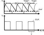
图3是振荡器DCO的构成概略的电路图,图4是从振荡器DCO输出的时钟信号CLK的时间变化的一例说明图。振荡器DCO如图3所示,包括:构成为恒流电路的第1电路M1;与第1电路M1构成电流镜电路(current mirror)的第2电路M2、第3电路M3;根据第2电路M2、M3的输出生成时钟信号CLK并输出的时钟信号输出电路CKO。第1电路M1包括:电阻器R;漏极经由电阻器R被供给电源电压Vdd(这里是电压V1)、栅极和漏极连接、源极接地的NMOS晶体管NM1。第2电路M2、M3具有相同的构成,包括:源极被供给电源电压Vdd的PMOS(P-channel Metal Oxide Semiconductor)晶体管PM1;栅极、漏极分别与晶体管PM1的栅极、漏极连接的NMOS晶体管NM2;栅极与晶体管NM1的栅极连接、漏极与晶体管NM2的漏极连接的NMOS晶体管NM3。在第2电路M2、M3的晶体管PM1的漏极和接地之间,经由开关SW1~SW5,电容器C1~C5相互并联连接。时钟信号输出电路CKO包括:比较第1电路M1的晶体管NM1的漏极与接地之间的电压即参考电压Vref和第2电路M2的晶体管PM1的漏极与接地之间的电压即作为电容器C1~C5的电极间电压的电容器电压Vcap1,将比较结果输出的比较器CMP11;比较参考电压Vref和第3电路M3的晶体管PM1的漏极与接地之间的电压即作为电容器C1~C5的电极间电压的电容器电压Vcap2,将比较结果输出的比较器CMP12;根据CMP11、12的比较结果,置位(set)或复位(reset)的触发器(Flip Flop)FF。触发器FF在电容器电压Vcap1为参考电压Vref以下时置位,将低电平的逻辑电压的信号作为时钟信号CLK输出,在电容器电压Vcap2为参考电压Vref以下时复位,将高电平的逻辑电压的信号作为时钟信号CLK输出,将与这样的时钟信号CLK反相的时钟信号CLKB也输出。另外,振荡器DCO还具备从控制逻辑电路46输入待机信号STB时将时钟信号CLK的电压固定为低电平的逻辑电压的没有图示的晶体管。FIG. 3 is a circuit diagram showing a schematic configuration of an oscillator DCO, and FIG. 4 is an explanatory diagram illustrating an example of a temporal change of a clock signal CLK output from the oscillator DCO. As shown in Figure 3, the oscillator DCO includes: a first circuit M1 constituted as a constant current circuit; a second circuit M2 and a third circuit M3 constituting a current mirror circuit (current mirror) with the first circuit M1; The outputs of M2 and M3 generate and output a clock signal CLK to a clock signal output circuit CKO. The first circuit M1 includes: a resistor R; and an NMOS transistor NM1 whose drain is supplied with a power supply voltage Vdd (here, voltage V1 ) via the resistor R, whose gate and drain are connected, and whose source is grounded. The second circuits M2 and M3 have the same configuration and include: a PMOS (P-channel Metal Oxide Semiconductor) transistor PM1 whose source is supplied with a power supply voltage Vdd; a gate and a drain connected to the gate and drain of the transistor PM1, respectively. NMOS transistor NM2; NMOS transistor NM3 having a gate connected to the gate of the transistor NM1 and a drain connected to the drain of the transistor NM2. Capacitors C1 to C5 are connected in parallel to each other via switches SW1 to SW5 between the drain of the transistor PM1 in the second circuits M2 and M3 and the ground. The clock signal output circuit CKO includes: comparing the voltage between the drain of the transistor NM1 of the first circuit M1 and the ground, that is, the reference voltage Vref, and the voltage between the drain of the transistor PM1 of the second circuit M2 and the ground, that is, capacitors C1~ The capacitor voltage Vcap1 of the inter-electrode voltage of C5, the comparator CMP11 that outputs the comparison result; compare the reference voltage Vref and the voltage between the drain of the transistor PM1 of the third circuit M3 and the ground, that is, the inter-electrode voltage of the capacitors C1-C5 The capacitor voltage Vcap2 is the comparator CMP12 that outputs the comparison result; according to the comparison results of CMP11 and 12, the flip-flop (Flip Flop) FF is set or reset. The flip-flop FF is set when the capacitor voltage Vcap1 is below the reference voltage Vref, outputs a low-level logic voltage signal as a clock signal CLK, and resets when the capacitor voltage Vcap2 is below the reference voltage Vref, and outputs a high-level logic voltage The signal of is output as a clock signal CLK, and a clock signal CLKB that is an inverted version of the clock signal CLK is also output. In addition, the oscillator DCO further includes a transistor (not shown) that fixes the voltage of the clock signal CLK to a low-level logic voltage when the standby signal STB is input from the
接着,说明这样构成的振荡器DCO的振荡操作。图4是参考电压Vref和电容器电压Vcap1、Vcap2和时钟信号CLK的电压随时间变化的一例说明图。第1电路M1、第2电路M2、第3电路M3构成电流镜电路,因此,流向各个电路的电流若设为Iref、Icap1、Icap2,则电流Iref、Icap1、Icap2互相相等,成为恒定。从而,参考电压Vref是恒定电压,可用下式(1)计算。式(1)中,值R是电阻器R的电阻值。如图4所示,第2电路M2的电容器电压Vcap1与电源电压Vdd为相等状态(图中″1″的状态)时,与开关SW1~SW5中导通的开关连接的电容器开始放电,电容器电压Vcap1的电压下降,成为与参考电压Vref相等的状态(图中″2″的状态)。此时,由于电流Icap1一定,因此电容器电压Vcap1以一定的时间变化率下降。电容器电压Vcap1的电压若变得比参考电压Vref小,则触发器FF输出的时钟信号CLK成为低电位而时钟信号CLKB成为高电位,第3电路M3的与开关SW1~SW5中导通的开关连接的电容器开始放电,电容器电压Vcap2的电压下降,成为与参考电压Vref相等的状态(图中″1″的状态)。此时,第2电路M2中与导通的开关连接的电容器被充电,电容器电压Vcap1上升。电容器电压Vcap2的电压下降,成为与参考电压Vref相等的状态后,从触发器FF输出的时钟信号CLK成为高电位而时钟信号CLKB成为低电位。这样,振荡器DCO振荡,生成时钟信号CLK。与开关SW1~SW5中导通的开关连接的电容器放电的时间T,即时钟信号CLK的半周期T,可用下式(2)计算,可根据式(2)和上述式(1)导出式(3)。另外,式(2)、(3)中,值C表示第2电路M2、第3电路中的与开关SW1~SW5中导通的开关连接的电容器的合成电容。这样,从振荡器DCO输出的时钟信号CLK的频率取决于电阻器R的电阻值R和第2电路M2、第3电路中的与开关SW1~SW5中导通的开关连接的电容器的合成电容C,因此,通过开关SW1~SW5中导通的开关的组合,可输出多个种类的频率的时钟信号CLK。实施例中,第2电路M2、第3电路M3采用相同的构成,因此,时钟信号CLK的占空比(时钟信号CLK成为高电位的时间除以周期2T后)成为0.5左右。以上,说明了振荡器DCO。Next, the oscillating operation of the thus configured oscillator DCO will be described. FIG. 4 is an explanatory diagram illustrating an example of changes in reference voltage Vref, capacitor voltages Vcap1 , Vcap2 , and clock signal CLK over time. The first circuit M1, the second circuit M2, and the third circuit M3 constitute a current mirror circuit. Therefore, if the currents flowing in each circuit are Iref, Icap1, and Icap2, the currents Iref, Icap1, and Icap2 are equal to each other and become constant. Therefore, the reference voltage Vref is a constant voltage and can be calculated by the following equation (1). In the formula (1), the value R is the resistance value of the resistor R. As shown in FIG. 4, when the capacitor voltage Vcap1 of the second circuit M2 is equal to the power supply voltage Vdd (the state of "1" in the figure), the capacitor connected to the conductive switch among the switches SW1 to SW5 starts to discharge, and the capacitor voltage The voltage of Vcap1 drops to become equal to the reference voltage Vref (the state of "2" in the figure). At this time, since the current Icap1 is constant, the capacitor voltage Vcap1 drops at a constant rate of change over time. When the voltage of the capacitor voltage Vcap1 becomes lower than the reference voltage Vref, the clock signal CLK output from the flip-flop FF becomes a low potential and the clock signal CLKB becomes a high potential, and the third circuit M3 is connected to the conductive switches SW1 to SW5. The capacitor starts to discharge, and the voltage of the capacitor voltage Vcap2 drops to become equal to the reference voltage Vref (the state of "1" in the figure). At this time, the capacitor connected to the turned-on switch in the second circuit M2 is charged, and the capacitor voltage Vcap1 rises. After the voltage of the capacitor voltage Vcap2 falls and becomes equal to the reference voltage Vref, the clock signal CLK output from the flip-flop FF becomes a high potential and the clock signal CLKB becomes a low potential. Thus, the oscillator DCO oscillates to generate the clock signal CLK. The discharge time T of the capacitors connected to the switches SW1-SW5 that are turned on, that is, the half period T of the clock signal CLK, can be calculated by the following formula (2), which can be derived from the formula (2) and the above formula (1) ( 3). In addition, in the formulas (2) and (3), the value C represents the composite capacitance of the capacitors connected to the switched on switches SW1 to SW5 in the second circuit M2 and the third circuit. In this way, the frequency of the clock signal CLK output from the oscillator DCO depends on the resistance value R of the resistor R and the combined capacitance C of the capacitors connected to the switches SW1 to SW5 in the second circuit M2 and the third circuit. Therefore, the clock signal CLK of a plurality of types of frequencies can be output by a combination of switches SW1 to SW5 that are turned on. In the embodiment, since the second circuit M2 and the third circuit M3 have the same configuration, the duty ratio of the clock signal CLK (the time during which the clock signal CLK becomes high potential divided by the period 2T) is about 0.5. The oscillator DCO has been described above.
Vref=Vdd-Iref·R (1)Vref=Vdd-Iref·R (1)
T=(Vdd-Vref)·C/Icap1 (2)T=(Vdd-Vref)·C/Icap1 (2)
T=RC (3)T=RC (3)
这里,再次使用图2说明。控制逻辑电路46在输出电压Vout为0V以上阈值Vth_L以下时,将频率模式FM设定成表示比较低的频率f0(例如,10MHz)的值0,在输出电压Vout比阈值Vth_L大而在阈值Vth_M以下时,将频率模式FM没定成表示比频率f0高的频率f1(例如,13.5MHz)的值1,在输出电压Vout比阈值Vth_M大而在阈值Vth_H以下时,将频率模式FM设定成表示比频率f1高的频率f2(例如,20MHz)的值2,在输出电压Vout比阈值Vth_H大时,将待机信号STB向振荡器DCO输出。Here, it demonstrates using FIG. 2 again. The
寄存器REG在内部具有寄存器Reg1、Reg2、Reg3,寄存器Reg1、Reg2、Reg3分别按预先频率模式FM的值存储开关SW1~SW5的导通截止的信息。从上述式(3)可明白,频率模式FM的值越小,从振荡器DCO应该输出的时钟信号CLK的频率越低(周期越长),与振荡器DCO连接的电容器C1~C5的合成电容必须越大,因此,使得频率模式FM的值越小则与振荡器DCO连接的电容器C1~C5的合成电容越大的各开关的导通截止信息预先存储在寄存器Reg1、Reg2、Reg3。The register REG has registers Reg1, Reg2, and Reg3 inside, and the registers Reg1, Reg2, and Reg3 respectively store on-off information of the switches SW1 to SW5 according to the value of the pre-frequency mode FM. It can be understood from the above formula (3) that the smaller the value of the frequency mode FM, the lower the frequency of the clock signal CLK that should be output from the oscillator DCO (the longer the period), and the combined capacitance of the capacitors C1 to C5 connected to the oscillator DCO Therefore, the smaller the value of the frequency mode FM, the larger the combined capacitance of the capacitors C1-C5 connected to the oscillator DCO. The on-off information of each switch is stored in the registers Reg1, Reg2, and Reg3 in advance.
从控制逻辑电路46输入频率模式FM后,选择器SL从寄存器REG读出与输入的频率模式FM的值对应的各开关的导通截止的信息,以开关SW1~SW5按照从寄存器REG读出的信息而导通截止的方式使振荡器DCO的开关SW1~SW5导通截止。另外,寄存器REG构成为可由与来自外部的时钟信号CLOCK同步输入的串行数据SDATA改写在寄存器REG存储的开关SW1~SW5的导通截止的信息,即使暂时在寄存器REG存储各开关的导通截止的信息后,也可以通过改写寄存器REG存储的信息,变更从振荡器DCO输出的时钟信号CLK的频率。After the frequency mode FM is input from the
接着,说明这样构成的升压电路40的操作。图5是从升压电路40输出的电压V2及从开关控制电路44输出的时钟信号CLK的时间变化的一例说明图。电压V1供给输入端子Vin后,开始升压操作,从控制逻辑电路46向选择器SL输出值0的频率模式FM,直到输出端子Vout的电压Vout超过阈值Vth_L为止。输入值0的频率模式FM的选择器SL从寄存器REG读出频率模式FM为值0时的各开关的导通截止的信息,切换振荡器DCO的第2电路M2、第3电路M3的开关SW1~SW5的导通截止。这样,开关SW1~SW5切换后,频率f0的时钟信号CLK从振荡器DCO经由输出缓冲器OB输入升压转换器42的晶体管N2的栅极,晶体管N2由频率f0的时钟信号CLK开关。从而,输出端子Vout的电压Vout比较迅速地上升。这样,电压Vout上升达到阈值VthL后,从控制逻辑电路46向选择器SL输出值1的频率模式FM,选择器SL从寄存器REG读出频率模式FM为值1时的各开关的导通截止的信息,切换振荡器DCO的第2电路M2、第3电路M3的开关SW1~SW5的导通截止。这样,开关SW1~SW5切换后,频率f1的时钟信号CLK从振荡器DCO经由输出缓冲器OB输入升压转换器42的晶体管N2的栅极,晶体管N2由比频率f0高的频率f1的时钟信号CLK开关。从而,输出端子Vout的电压Vout进一步上升,但是由于频率f1比频率f0高,电压Vout更缓慢上升。电压Vout达到阈值Vth_M后,从控制逻辑电路46向选择器SL输出值2的频率模式FM,选择器SL从寄存器REG读出频率模式FM为值2时的各开关的导通截止的信息,切换振荡器DCO的第2电路M2、第3电路M3的开关SW1~SW5的导通截止。这样,开关SW1~SW5切换后,频率f2的时钟信号CLK从振荡器DCO经由输出缓冲器OB输入升压转换器42的晶体管N2的栅极,晶体管N2由比频率f1高的频率f2的时钟信号CLK开关。从而,输出端子Vout的电压Vout进一步上升,但是由于频率f2比频率f1高,因此电压Vout更缓慢上升。电压Vout达到阈值Vth_H(与电压V2相同)后,从控制逻辑电路46向振荡器DCO输出待机信号STB,输入待机信号STB的振荡器DCO停止振荡操作,电压Vout的上升停止,升压电路40的升压操作停止。通过这样的操作,可使供给输入端子Vin的电压V1升压到电压V2为止,由于输出电压Vout的电压越接近电压V2则振荡器DCO的振荡频率设为越高,因此可使输出电压Vout缓慢升压。因此,可更适当地将输入的电压Vin升压到电压V2。另外,这样,升压操作停止后,电压Vout开始缓缓降低,但是,电压Vout低于阈值Vth_H(电压V2)后(图中,时间为2.6μs时),再次开始振荡器DCO的振荡操作使电压Vout上升,因此可将电压Vout升压到电压V2。Next, the operation of the
这样构成的升压电路40包含电感器L,需要比较大的面积,因此认为若在闪速存储器芯片22搭载,则闪速存储器芯片22的面积变大,但是,实施例的集成电路装置10中,升压电路40搭载于在层叠体24的上面配置的介入层30,因此与将升压电路40在层叠体24的闪速存储器芯片22搭载的情况相比,可实现装置的小型化。另外,在进行相对于输入电压Vin以较高比率使输出电压Vout升压的高放大率升压的场合,若利用采用并联连接的多个电容器使输入电压升压的充电泵,则需要更多的电容器,因此认为面积变大,升压的效率降低,但是,即使在通过采用升压转换器42进行这样的高放大率的升压的场合,通过调节电感器L、电容器CL、电阻器RL也可获得期望的升压性能,与采用充电泵的场合比,可实现装置的小型化和效率降低的抑制。The
根据以上说明的第1实施例的集成电路装置10,升压电路40搭载于层叠体24的上面配置的介入层30,因此可实现装置的小型化。另外,采用升压转换器作为升压电路40,因此与采用多个电容器并联连接而成的充电泵的情况比,可实现装置的小型化。而且,输出电压Vout越接近电压V2而振荡器DCO的振荡频率设为越高,因此可使输出电压Vout缓慢升压。从而,可更适当地将输入的电压Vin升压到电压V2。According to the
第1实施例的集成电路装置10中,采用3种频率的时钟信号CLK开关晶体管N2,但是也可以采用3种以上的频率的时钟信号CLK或者2种以下的频率的时钟信号CLK。该场合,根据时钟信号CLK的种类,通过适宜变更开关控制电路44的振荡器DCO的构成和寄存器REG存储的信息等,可变更时钟信号CLK的种类。In the
第1实施例的集成电路装置10中,将第2电路M2、第3电路M3设为相同的构成,即通过切换开关SW1~SW5的导通截止而输出占空比为0.5的时钟信号CLK,但是,也可以通过相互独立切换第2电路M2的开关SW1~SW5和第3电路M3的开关SW1~SW5,使时钟信号CLK的占空比比0.5大或者比0.5小。该场合,寄存器REG按照要预先输出的时钟信号CLK的占空比,并按照第2电路M2、第3电路M3的各电路,预先存储开关SW1~SW5的导通截止的信息,控制逻辑电路46根据输出电压Vout向选择器SL输出要输出的时钟信号CLK的占空比的信息,选择器SL根据来自控制逻辑电路46的信息,从寄存器REG读出对应的第2电路M2、第3电路M3的开关SW1~SW5的信息,采用读出的信息,相互独立地导通截止第2电路M2、第3电路M3的开关SW1~SW5。In the
接着,说明第2实施例的集成电路装置110。第2实施例的集成电路装置110除了在介入层30搭载的升压电路140的构成与第1实施例的升压电路40的构成不同外,具有与第1实施例的集成电路装置10同样的构成。从而,这里为了避免重复说明,集成电路装置110的构成中与第1实施例的集成电路装置10同样的构成附上相同的符号,省略详细的说明。Next, the integrated circuit device 110 of the second embodiment will be described. The integrated circuit device 110 of the second embodiment has the same configuration as the
图6是升压电路140的构成的概略的电路图。升压电路140具备:使供给输入端子Vin的电压V1升压后从输出端子Vout向闪速存储器输出的升压转换器142;控制升压转换器142的开关控制电路144。升压转换器142具有:在被供给电压V1的输入端子Vin和输出电压V2的输出端子Vout之间串联连接的电感器L;栅极和源极相互连接,源极与电感器L连接而漏极与输出端子Vout连接的晶体管N1;在电感器L和晶体管N1之间从电感器L看,与输出端子Vout并联连接的晶体管N2。晶体管N2根据来自开关控制电路144的时钟信号CLK进行开关控制。FIG. 6 is a schematic circuit diagram of the configuration of the
开关控制电路144包括:输出时钟信号CLK的振荡器DCO1;将来自振荡器DCO1的时钟信号CLK以适当定时输入升压转换器142的晶体管N2的栅极的输出缓冲器OB;检测输出端子Vout的输出电压Vout,将检测值变换为数字值的A/D转换器AD;根据从A/D转换器AD输入的输出电压Vout和将输出电压Vout延迟了以作为接近时钟信号CLK的周期的时间而预先设定的规定时间T的延迟电压Vdlay的差值,运算时钟信号CLK的1周期量的电压变化量dVout的延迟运算电路D1;检测输入端子Vin的输入电压Vin,将检测值变换为数字值的输入电压检测电路VD;被分别输入来自A/D转换器AD的输出电压Vout、来自延迟运算电路D1的电压变化量dVout、来自输入电压检测电路VD的输入电压Vin,并且,运算并输出要从振荡器DCO1输出的时钟信号CLK在1周期使晶体管N2导通的导通时间Ton和在1周期使晶体管N2截止的截止时间Toff,或者输出用于停止振荡器DCO的操作的待机信号STB的控制逻辑电路146。The switch control circuit 144 includes: an oscillator DCO1 that outputs a clock signal CLK; an output buffer OB that inputs the clock signal CLK from the oscillator DCO1 to the gate of the transistor N2 of the boost converter 142 at an appropriate timing; The output voltage Vout, the A/D converter AD that converts the detected value into a digital value; based on the output voltage Vout input from the A/D converter AD and the time that the output voltage Vout is delayed so as to be close to the period of the clock signal CLK The delay calculation circuit D1 that calculates the difference of the delay voltage Vdlay for a predetermined time T in advance and calculates the voltage change dVout of one cycle of the clock signal CLK; detects the input voltage Vin of the input terminal Vin, and converts the detected value into a digital value The input voltage detection circuit VD of the input voltage detection circuit VD; the output voltage Vout from the A/D converter AD, the voltage change dVout from the delay operation circuit D1, and the input voltage Vin from the input voltage detection circuit VD are respectively input, and the operation and output The clock signal CLK output from the oscillator DCO1 has an on-time Ton for turning on the transistor N2 for one cycle and an off-time Toff for turning the transistor N2 off for one cycle, or outputs a standby signal STB for stopping the operation of the oscillator DCO Control logic circuit 146 .
控制逻辑电路146具有可存储信息的存储部146a、146b和采用存储部146a、146b存储的信息运算时钟信号CLK的导通时间Ton、截止时间Toff的运算部146c,在存储部M1存储输出电压Vout、电压变化量dVout、输入电压Vin、通过后述的方法推定与输出端子Vout连接的作为负载电容量的推定负载电容量Cle,在存储部M2存储对照映射(map),该对照映射为相对于与输出端子Vout连接的负载电容量Cl和输出电压Vout,在输出电压Vout从电压V1升压到电压V2为止升由压转换器142消耗的能量成为较低的时钟信号CLK的导通时间Ton、截止时间Toff的关系。另外,在存储部146a中,到后述的第1次的升压结束为止,作为推定负载电容量Cle,存储值C1(例如,100pF),作为输入电压Vin,存储值Vref(例如,1.8V)。另外,控制逻辑电路146在输入的输出电压Vout为规定电压V2以上时,向振荡器DCO1输出待机信号STB。The
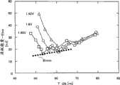
这里,说明存储部146b存储的对照映射。图7是输入电压Vin为一定时的输出端子Vout所连接的负载电容量Cl和导通时间Ton以及将输出电压Vout从电压V1升压到电压V2为止由升压转换器142消耗的能量即消耗能量Ebo的关系的说明图,图8是输入电压Vin一定时的负载电容量Cl和截止时间Toff以及消耗能量Ebo的关系的说明图。图7中,截止时间Toff,按每个负载电容量Cl,设为图8中消耗能量Ebo成为最低的时间,图8中,导通时间Ton,按每个负载电容量Cl,设为图7中消耗能量Ebo成为最低的时间。在负载电容量Cl为一定的场合,消耗能量Ebo如图示,在某导通时间Ton、截止时间Toff成为最小功率Pmin,成为最小值Pmin的导通时间Ton、截止时间Toff具有随着负载电容量Cl变大而变长的倾向。图9是负载电容量Cl一定时的输入电压Vin和导通时间Ton以及消耗能量Ebo的关系的说明图,图10是负载电容量Cl一定时的输入电压Vin和截止时间Toff以及消耗能量Ebo的关系的说明图。图9中,截止时间Toff,按每个输入电压Vin,设为图10中消耗能量Ebo成为最低的时间,图10中,导通时间Ton,按每个输入电压Vin,成为图9中消耗能量Ebo成为最低的时间。在输入电压Vin为一定的场合,消耗能量Ebo如图示,在某导通时间Ton、截止时间Toff成为最小值Emin。从而,针对输入电压Vin和负载电容量Cl,可确定消耗能量Ebo成为最小值Emin的时钟信号CLK的导通时间Ton、截止时间Toff。图11是输入电压Vin一定(例如,1.8V)时负载电容量Cl和消耗能量Ebo成为最小值Emin的导通时间Ton、截止时间Toff的关系的一例说明图,图12是负载电容量Cl一定(例如,100pF)时输入电压Vin和消耗能量Ebo成为最小值Emin的导通时间Ton、截止时间Toff的一例的说明图。从而,针对负载电容量Cl和输入电压Vin,若以消耗能量Ebo成为最小的导通时间Ton、截止时间Toff,即,消耗能量Ebo成为最小的频率及占空比的时钟信号CLK,来开关升压转换器142的晶体管N2,则可有效使电压Vout升压。对照映射作为针对负载电容量Cl和输入电压Vin,消耗能量Ebo成为最小的导通时间Ton、截止时间Toff的关系,预先通过实验、解析等求出。Here, the collation map stored in the
控制逻辑电路146的运算部146c,检测输入的输出电压Vout因晶体管N2的1次开关而导致的上升结束后的上升结束定时,检测到上升结束定时后,采用在存储部146a存储的时钟信号CLK的导通时间Ton、截止时间Toff推定负载电容量Cle、输入电压Vin、输出电压Vout,运算出输出端子Vout与推定负载电容量Cle连接的状态下以导通时间Ton、截止时间Toff的时钟信号CLK开关晶体管N2时产生的电压变化量的推定值dVe。然后,比较输入的电压变化量dVout和运算的推定值dVe,输入的电压变化量dVout和运算的推定值dVe在规定范围内一致时(电压变化量dVout和推定值dVe的差值小于规定值时),判断输出端子Vout与在存储部146a存储的推定负载电容量Cle的负载连接,将存储部146a存储的导通时间Ton、截止时间Toff向振荡器DCO1输出,并在控制逻辑电路146的存储部146a存储输入的输入电压Vin、输出电压Vout。输入的电压变化量dVout和运算的推定值dVe在规定范围内不一致时(电压变化量dVout和推定值dVe的差值在规定值以上时),判断与输出端子Vout连接的负载的电容量发生了变更,将使以导通时间Ton、截止时间Toff的时钟信号CLK开关晶体管N2时的电压变化量成为输入的电压变化量dVout的负载电容量设定为推定负载电容量Cle,参照存储部146b存储的对照映射,向振荡器DCO1输出推定负载电容量Cle和与输入电压Vin对应的导通时间Ton、截止时间Toff。例如,输入的电压变化量dVout比运算的推定值dVe大时,将比存储部146a存储的负载电容量小的负载电容量设定为推定负载电容量Cle。这样,将导通时间Ton、截止时间Toff向振荡器DCO1输出后,在存储部146a存储输入的输出电压Vout、输入电压Vin、新设定的导通时间Ton、截止时间Toff、推定负载电容量Cle。通过这样的处理,在存储部146a存储了前一循环的升压操作中的输出电压Vout、输入电压Vin、导通时间Ton、截止时间Toff、推定负载电容量Cle。这样,控制逻辑电路146采用前一循环的升压操作中的输出电压Vout、输入电压Vin、导通时间Ton、截止时间Toff、推定负载电容量Cle,推定与输出端子Vout连接的负载电容量,相对于推定的负载电容量(推定负载电容量Cle)和输入电压Vin,将可高效驱动升压转换器142的导通时间Ton、截止时间Toff向振荡器DCO1输出。另外,最初进行升压时,由于在存储部146b存储前一循环的升压操作中的输出电压Vout、输入电压Vin、导通时间Ton、截止时间Toff、推定负载电容量Cle,因此,采用从输入电压检测电路VD输入的输入电压Vin、从A/D转换器AD输入的输出电压Vout、作为推定负载电容量Cle预先在存储部146b存储的电容Cref(例如,100pF),设定导通时间Ton、截止时间Toff,向振荡器DCO1输出。The
图13是振荡器DCO1的构成的概略的电路图。振荡器DCO1如图示,除了在第2电路M2、第3电路M3的晶体管PM1的漏极和接地之间,电容器C1s、C2s不经由开关而连接方面,第2电路M2、第3电路M3中在晶体管PM1的漏极和接地之间,电容器C11~C25经由相互独立控制的开关SW11~SW25而连接方面以及电容器C11~C25的电容互异的方面,具有与第1实施例的振荡器DCO同样的构成。从而,从振荡器DCO1输出的时钟信号CLK的频率及占空比,由电阻器R的电阻值R和第2电路M2、第3电路中不经由开关而连接的电容器C1s、C2s、与开关SW11~SW25中导通的开关连接的电容器的合成电容C确定。即,通过开关SW11~SW25的导通截止的组合,可调节输出的时钟信号CLK的频率及占空比,即,导通时间Ton、截止时间Toff。另外,实施例中,电容器C1s、C2s不经由开关与晶体管PM1的漏极连接,但是,电容器C1s、C2s也可以常时与晶体管PM1的漏极连接,也可以经由常时导通的开关与晶体管PM1的漏极连接。FIG. 13 is a schematic circuit diagram of the configuration of the oscillator DCO1. As shown in the figure, the oscillator DCO1 is connected between the drain of the transistor PM1 of the second circuit M2 and the third circuit M3 and the ground, and the capacitors C1s and C2s are connected without a switch. In the second circuit M2 and the third circuit M3 Between the drain of the transistor PM1 and the ground, the capacitors C11 to C25 are connected via the switches SW11 to SW25 independently controlled, and the capacitances of the capacitors C11 to C25 are different from each other, which is the same as that of the oscillator DCO of the first embodiment. composition. Therefore, the frequency and duty ratio of the clock signal CLK output from the oscillator DCO1 are determined by the resistance value R of the resistor R and the capacitors C1s and C2s connected without switches in the second circuit M2 and the third circuit, and the switch SW11. The resultant capacitance C of the capacitors connected by switches that are turned on in ~SW25 is determined. That is, the frequency and duty cycle of the output clock signal CLK, ie, the on-time Ton and the off-time Toff, can be adjusted through the on-off combination of the switches SW11˜SW25. In addition, in the embodiment, the capacitors C1s and C2s are not connected to the drain of the transistor PM1 through a switch, but the capacitors C1s and C2s can also be connected to the drain of the transistor PM1 at all times, or can be connected to the transistor through a switch that is always on. Drain connection of PM1.
时钟信号CLK的导通时间Ton、截止时间Toff可用下式(4)、(5)计算。式(4)中,C1n是第2电路M2中与开关SW11~SW15中导通的开关连接的电容器的合成电容,C2n是第3电路M3中与开关SW21~SW25中导通的开关连接的电容器的合成电容。图14是振荡器DCO1的第1电路M1的晶体管NM1的漏极和接地之间的电压即参考电压Vref和第2电路M2、第3电路M3的各自的晶体管PM1的漏极和接地之间的电压即电容器电压Vcap1(实线)、Vcap2(虚线)以及时钟信号CLK的电压随时间变化的一例说明图。振荡器DCO1,首先以开关SW11~SW25截止的状态开始时钟信号CLK的输出,由控制逻辑电路146在输出导通时间Ton、截止时间Toff时(图中,例如时刻t1、t2)切换与导通时间Ton、截止时间Toff对应的开关SW11~SW25的导通截止。这是因为,由控制逻辑电路146设定导通时间Ton、截止时间Toff需要某程度的时间,因此,设置不经由开关与晶体管PM1连接的电容器C1s、C2s,确保由控制逻辑电路146设定导通时间Ton、截止时间Toff所需时间程度的导通时间Ton,从而,从控制逻辑电路146输出导通时间Ton、截止时间Toff前,可避免时钟信号CLK使晶体管N2导通截止而进行升压操作。这样的控制逻辑电路146,可根据控制逻辑电路146的性能等预先设定导通时间Ton、截止时间Toff的设定所需的时间,因此,电容器C1s、C2s的电容可根据由控制逻辑电路146设定导通时间Ton、截止时间Toff所需的时间等确定。通过这样构成的振荡器DCO1,可输出期望的导通时间Ton、截止时间Toff的时钟信号CLK。The on-time Ton and off-time Toff of the clock signal CLK can be calculated by the following equations (4) and (5). In formula (4), C1n is the composite capacitance of the capacitor connected to the switches SW11~SW15 that are turned on in the second circuit M2, and C2n is the capacitor connected to the switches SW21~SW25 that are turned on in the third circuit M3 synthetic capacitance. 14 is the voltage between the drain of the transistor NM1 of the first circuit M1 of the oscillator DCO1 and the ground, that is, the reference voltage Vref, and the voltage between the drains of the respective transistors PM1 of the second circuit M2 and the third circuit M3 and the ground. It is an explanatory diagram of an example of voltage, that is, capacitor voltages Vcap1 (solid line) and Vcap2 (dashed line), and the voltage of the clock signal CLK changing with time. The oscillator DCO1 first starts to output the clock signal CLK with the switches SW11-SW25 turned off, and is switched and turned on by the
Ton=(C1s+C1n)·(Vdd-Vcap1)/Iref=R·(C1s+C1n) (4)Ton=(C1s+C1n)·(Vdd-Vcap1)/Iref=R·(C1s+C1n) (4)
Toff=(C2s+C1n)·(Vdd-Vcap2)/lref=R·(C2s+C2n) (5)Toff=(C2s+C1n)·(Vdd-Vcap2)/lref=R·(C2s+C2n) (5)
接着,说明这样构成的升压电路140的操作。图15是负载电容量Cl为100pF、800pF时的升压开始后到第1次的升压、第2次的升压结束为止的输出电压Vout及时钟信号CLK随时间变化的一例说明图,图16是输出端子Vout的负载在负载电容量Cl为100pF、800pF时开始升压后3微秒期间的输出电压Vout及从开关控制电路144输出的时钟信号CLK随时间变化的一例说明图。电压Vin供给输入端子Vin,开始升压操作后,开关控制电路144的控制逻辑电路146,首先采用从输入电压检测电路VD输入的输入电压Vin和/或从A/D转换器AD输入的输出电压Vout、存储部146b存储的推定负载电容量Cle(值Cref),设定导通时间Ton、截止时间Toff,向振荡器DCO1输出,并将输入的输出电压Vout和输入电压Vin、设定的导通时间Ton、截止时间Tof、推定负载电容量Cle在存储部146a存储。输入了导通时间Ton、截止时间Toff的振荡器DCO1切换开关SW11~SW25的导通截止,使得仅仅与输入的导通时间Ton、截止时间Tof附应的开关SW11~SW25导通。这样,开关SW11~SW25切换后,来自振荡器DCO1的设定的导通时间Ton、截止时间Toff的时钟信号CLK经由输出缓冲器OB输入升压转换器142的晶体管N2的栅极,晶体管N2以设定的导通时间Ton、截止时间Toff的时钟信号CLK开关1次。这样,第1次的升压操作结束。即,第1次的升压操作中,推定负载电容量Cl为值Cref,将由负载电容量C1和现在输入的输入电压Vin可高效驱动升压转换器142的导通时间Ton、截止时间Toff,即,可高效驱动升压转换器142的频率及占空比的时钟信号CLK,输入晶体管N2的栅极,进行升压。从而,不管实际与输出端子Vout连接的负载电容量Cl如何,输入电压Vin为一定的场合,第1次的升压操作在推定负载电容量Cl为100pF后进行升压,因此导通时间Ton、截止时间Toff相同。Next, the operation of the
接着,开始第2次以下的升压操作。第2次以下的升压操作中,开关控制电路144的控制逻辑电路146运算电压变化量的推定值dVe,比较来自延迟运算电路D1的电压变化量dVout和运算的电压变化量的推定值dVe,将与比较结果相应的导通时间Ton、截止时间Toff向振荡器DCO1输出。负载电容量Cl为100pF时,第1次的升压产生的电压变化量dVout与推定负载电容量Cl为100pF时的电压变化量的推定值Cle大致相同,因此,推定负载电容量Cle为100pF时,以可高效驱动升压转换器142的导通时间Ton、截止时间Toff进行晶体管N2的开关。另一方面,在负载电容量Cl为800pF时,第1次的升压产生的电压变化量dVout比电压变化量的推定值dVe小,因此,根据第1次的升压产生的电压变化量dVout,将更大的电容量(例如,800pF)设定为推定负载电容量Cl,以与推定负载电容量Cl和输入电压Vin对应的导通时间Ton、截止时间Toff进行晶体管N2的开关。从而,第2次以下的升压操作中,根据前一循环的升压操作推定实际连接的负载电容量Cl,对于推定的负载电容量Cl和输入电压Vin,可一边高效驱动升压转换器142,一边将输出端子Vout的电压Vout升压到规定电压V2为止。Next, the second and subsequent boosting operations are started. In the second and subsequent step-up operations, the
这样进行升压操作,电压Vout达到规定电压V2后,从控制逻辑146向振荡器DCO1输出待机信号STB,输入待机信号STB的振荡器DCO停止振荡操作,升压电路40的操作停止。从而,电压Vout达到规定电压V2为止期间,即使负载电容量、输入电压Vin变动也可高效驱动升压转换器142,同时,由于电压Vout升压,可以实现升压转换器142的能量效率的提高。特别是,在集成电路装置110搭载于进行存储交织的CPU(Central Processing Unit)时,考虑在升压电路140进行升压的中途,要供给电压的闪速存储器的存储器存储体被切换,与输出端子Vout连接的负载电容量变化的情况,但是即使在这样的场合,也可以高效进行输出电压Vout的升压。The boosting operation is performed in this way, and when the voltage Vout reaches the predetermined voltage V2, the
这样构成的升压电路140包含电感器L,需要比较大的面积,因此认为若在闪速存储器芯片22搭载,则闪速存储器芯片22的面积变大,但是,实施例的集成电路装置10中在层叠体24的上面配置的介入层30搭载升压电路140,因此与将升压电路410搭载于层叠体24的闪速存储器芯片22的情况比,可实现装置的小型化。另外,在进行相对于输入电压Vin以较高比率使输出电压Vout升压的高放大率升压的场合,若利用采用并联连接的多个电容器使输入电压升压的充电泵,则需要更多的电容器,因此认为面积变大,升压的效率降低,但是,即使在通过采用升压转换器42进行这样的高放大率的升压的场合,通过调节电感器L、电容器CL、电阻器RL也可获得期望的升压性能,与采用充电泵的场合比,可实现装置的小型化和效率降低的抑制。The
根据以上说明的第2实施例的集成电路装置110,升压电路140搭载于层叠体24的上面配置的介入层30,因此可实现装置的小型化。另外,采用升压转换器作为升压电路140,因此与采用多个电容器并联连接而成的充电泵的情况比,可实现装置的小型化。而且,推定实际连接的负载电容量Cl,相对于推定的负载电容量Cl和输入电压Vin,可高效驱动升压转换器142的同时,可将输出端子Vout的电压Vout升压到规定电压V2为止。According to the integrated circuit device 110 of the second embodiment described above, the
第2实施例的集成电路装置110中,在控制逻辑电路146的存储部146b预先存储对照映射,但是,也可以预先通过实验、解析等求出确定负载电容量Cl和输入电压Vin与消耗能量Ebo成为最小的导通时间Ton、截止时间Toff的关系的公式,采用这样的公式,相对于负载电容量Cl和输入电压Vin,运算消耗能量Ebo成为最小的导通时间Ton、截止时间Toff。In the integrated circuit device 110 of the second embodiment, the comparison map is stored in advance in the
第2实施例的集成电路装置110中,振荡器DCO1在由控制逻辑电路146输出导通时间Ton、截止时间Toff的定时切换与导通时间Ton、截止时间Toff对应的开关SW11~SW25的导通截止,但是,也可以在晶体管N2截止的定时切换与导通时间Ton、截止时间Toff对应的开关SW11~SW25的导通截止。In the integrated circuit device 110 of the second embodiment, the oscillator DCO1 switches the conduction of the switches SW11 to SW25 corresponding to the on-time Ton and the off-time Toff at the timing when the
第2实施例的集成电路装置110中,相对于推定的负载电容量Cl和输入电压Vin,采用可高效驱动升压转换器142的导通时间Ton、截止时间Toff的时钟信号CLK来开关晶体管N2,但是,也可以不考虑输入电压Vin,仅仅相对于推定的负载电容量Cl,采用可高效驱动升压转换器142的导通时间Ton、截止时间Toff的时钟信号CLK,也可以不考虑负载电容量Cl,仅仅相对于输入电压Vin,采用可高效驱动升压转换器142的导通时间Ton、截止时间Toff的时钟信号CLK。In the integrated circuit device 110 of the second embodiment, the transistor N2 is switched by using the clock signal CLK capable of efficiently driving the ON time Ton and the OFF time Toff of the
第1、第2实施例的集成电路装置10、110中,升压转换器42、142具备:在电感器L和晶体管N1之间从电感器L看与输出端子Vout并联连接的耗尽型的NMOS晶体管N2,但是,只要具备在电感器L和晶体管N1之间从电感器L看与输出端子Vout并联且由时钟信号CLK开关的元件即可,因此,如图17例示的变形例的升压转换器42B那样,也可以取代耗尽型的NMOS晶体管N2,而具备在电感器L和晶体管N1之间连接的耗尽型的NMOS晶体管N21(以下称为晶体管N21)和与晶体管N21串联的增强型的NMOS晶体管N22(以下称为晶体管N22),将晶体管N21的栅极的电压固定为规定电压VH并向晶体管N22的栅极输入时钟信号CLK。这里,规定电压VH优选为电压V1和电压V2之间的电压(例如,3.6V)。另外,升压转换器42、142设为具备栅极和源极相互连接、源极与电感器L连接而漏极与输出端子Vout连接的增强型的NMOS晶体管N1,但是,只要具备在电感器L和输出端子Vout之间串联连接、将电流整流为从输入端子Vin朝向输出端子Vout的方向的整流元件即可,因此也可以取代晶体管N1而具备二极管。In the
第1、第2实施例的集成电路装置10、110中,闪速存储器芯片22设为以与电源电压相同的电压V1和比电压V1高的电压V2操作,但是,也可以使闪速存储器芯片22以比电源电压高而比电压V2低的电压V3和电压V2操作。该场合,在介入层30搭载升压电路40、140以及将电压V1升压到电压V3的升压电路即可。In the
第1、第2实施例的集成电路装置10、110中,设为在层叠体24的上面配置介入层30,但是,也可以在下面配置。另外,也可以在介入层30上层叠其他集成电路芯片和介入层。In the
第1、第2实施例中,集成电路装置10用于SSD,层叠体24由DRAM芯片20和闪速存储器芯片22层叠而成,但是,集成电路10也可以在不同于SSD的装置中采用,例如,集成电路装置也可以用于微计算机,层叠体也可以由搭载MPU(Micro Processing Unit)的芯片等层叠而成。另外,也可以适用于计算机以外的电子设备。In the first and second embodiments, the
以上,用实施例说明了本发明的最佳实施例,但是本发明不限于这样的实施例,在不脱离本发明的要旨的范围内可以各种各样的形态实施。As mentioned above, the preferred embodiment of the present invention was described using the embodiment, but the present invention is not limited to such embodiment, and can be implemented in various forms without departing from the gist of the present invention.
产业上的利用可能性Industrial Utilization Possibility
本发明可适用于集成电路装置的制造产业等。The present invention is applicable to the manufacturing industry of integrated circuit devices and the like.
Claims (15)
Translated fromChineseApplications Claiming Priority (3)
| Application Number | Priority Date | Filing Date | Title |
|---|---|---|---|
| JP2008270062 | 2008-10-20 | ||
| JP2008-270062 | 2008-10-20 | ||
| PCT/JP2009/057773WO2010047140A1 (en) | 2008-10-20 | 2009-04-17 | Integrated circuit device |
Publications (1)
| Publication Number | Publication Date |
|---|---|
| CN102187400Atrue CN102187400A (en) | 2011-09-14 |
Family
ID=42119190
Family Applications (1)
| Application Number | Title | Priority Date | Filing Date |
|---|---|---|---|
| CN2009801416666APendingCN102187400A (en) | 2008-10-20 | 2009-04-17 | Integrated circuit device |
Country Status (4)
| Country | Link |
|---|---|
| US (1) | US8742838B2 (en) |
| JP (1) | JP5504507B2 (en) |
| CN (1) | CN102187400A (en) |
| WO (1) | WO2010047140A1 (en) |
Cited By (3)
| Publication number | Priority date | Publication date | Assignee | Title |
|---|---|---|---|---|
| CN103312163A (en)* | 2012-03-13 | 2013-09-18 | 上海华虹集成电路有限责任公司 | PFM (Pulse Frequency Modulation) switching circuit of switch power supply |
| CN105264743A (en)* | 2013-06-26 | 2016-01-20 | 英特尔公司 | Power management in multi-die assemblies |
| CN115116499A (en)* | 2021-03-18 | 2022-09-27 | 铠侠股份有限公司 | Semiconductor memory device with a plurality of memory cells |
Families Citing this family (16)
| Publication number | Priority date | Publication date | Assignee | Title |
|---|---|---|---|---|
| US8289065B2 (en)* | 2008-09-23 | 2012-10-16 | Transphorm Inc. | Inductive load power switching circuits |
| JP5709197B2 (en)* | 2010-05-21 | 2015-04-30 | 国立大学法人 東京大学 | Integrated circuit device |
| WO2011155295A1 (en)* | 2010-06-10 | 2011-12-15 | Semiconductor Energy Laboratory Co., Ltd. | Dc/dc converter, power supply circuit, and semiconductor device |
| US8363418B2 (en) | 2011-04-18 | 2013-01-29 | Morgan/Weiss Technologies Inc. | Above motherboard interposer with peripheral circuits |
| US9036443B2 (en) | 2011-05-18 | 2015-05-19 | The University Of Tokyo | Integrated circuit device |
| JP5387629B2 (en)* | 2011-07-30 | 2014-01-15 | 株式会社デンソー | DCDC converter control device |
| US10263519B2 (en) | 2015-07-23 | 2019-04-16 | International Business Machines Corporation | Resonant virtual supply booster for synchronous digital circuits having a predictable evaluate time |
| US9612614B2 (en) | 2015-07-31 | 2017-04-04 | International Business Machines Corporation | Pulse-drive resonant clock with on-the-fly mode change |
| US9634654B2 (en) | 2015-08-07 | 2017-04-25 | International Business Machines Corporation | Sequenced pulse-width adjustment in a resonant clocking circuit |
| US9568548B1 (en) | 2015-10-14 | 2017-02-14 | International Business Machines Corporation | Measurement of signal delays in microprocessor integrated circuits with sub-picosecond accuracy using frequency stepping |
| US20170213951A1 (en)* | 2016-01-27 | 2017-07-27 | Korea Research Institute Of Standards And Science | Flexible thin multi-layered thermoelectric energy generating module, voltage boosting module using super capacitor, and portable thermoelectric charging apparatus using the same |
| JP2019128829A (en)* | 2018-01-25 | 2019-08-01 | 東芝メモリ株式会社 | Semiconductor storage and memory system |
| US10700028B2 (en) | 2018-02-09 | 2020-06-30 | Sandisk Technologies Llc | Vertical chip interposer and method of making a chip assembly containing the vertical chip interposer |
| US10879260B2 (en) | 2019-02-28 | 2020-12-29 | Sandisk Technologies Llc | Bonded assembly of a support die and plural memory dies containing laterally shifted vertical interconnections and methods for making the same |
| US10839918B1 (en)* | 2019-06-24 | 2020-11-17 | Sandisk Technologies Llc | Boost converter in memory chip |
| TWI780980B (en)* | 2021-11-10 | 2022-10-11 | 創意電子股份有限公司 | Semiconductor chiplet device |
Citations (2)
| Publication number | Priority date | Publication date | Assignee | Title |
|---|---|---|---|---|
| US20080009124A1 (en)* | 2006-07-07 | 2008-01-10 | Masakazu Ishino | Method of forming a semiconductor device |
| TW200838141A (en)* | 2007-03-07 | 2008-09-16 | Orise Technology Co Ltd | Method for stabling voltage, pulse frequency modulating circuit and power supply using the same |
Family Cites Families (11)
| Publication number | Priority date | Publication date | Assignee | Title |
|---|---|---|---|---|
| TW521858U (en)* | 2000-04-28 | 2003-02-21 | Agc Technology Inc | Integrated circuit apparatus with expandable memory |
| US6434044B1 (en)* | 2001-02-16 | 2002-08-13 | Sandisk Corporation | Method and system for generation and distribution of supply voltages in memory systems |
| US6577535B2 (en)* | 2001-02-16 | 2003-06-10 | Sandisk Corporation | Method and system for distributed power generation in multi-chip memory systems |
| US7639542B2 (en)* | 2006-05-15 | 2009-12-29 | Apple Inc. | Maintenance operations for multi-level data storage cells |
| US7619945B2 (en)* | 2006-08-18 | 2009-11-17 | Unity Semiconductor Corporation | Memory power management |
| JP2008071953A (en) | 2006-09-14 | 2008-03-27 | Nec Electronics Corp | Semiconductor device |
| JP2008071935A (en)* | 2006-09-14 | 2008-03-27 | Toshiba Corp | Semiconductor device |
| KR100843148B1 (en)* | 2006-12-22 | 2008-07-02 | 삼성전자주식회사 | Liquid crystal display device, connector for test of liquid crystal display device and test method thereof |
| JP2009003991A (en)* | 2007-06-19 | 2009-01-08 | Toshiba Corp | Semiconductor device and semiconductor memory test device |
| JP2009210448A (en)* | 2008-03-05 | 2009-09-17 | Toshiba Corp | Semiconductor device |
| US7894230B2 (en)* | 2009-02-24 | 2011-02-22 | Mosaid Technologies Incorporated | Stacked semiconductor devices including a master device |
- 2009
- 2009-04-17CNCN2009801416666Apatent/CN102187400A/enactivePending
- 2009-04-17JPJP2010534730Apatent/JP5504507B2/enactiveActive
- 2009-04-17USUS13/123,811patent/US8742838B2/ennot_activeExpired - Fee Related
- 2009-04-17WOPCT/JP2009/057773patent/WO2010047140A1/enactiveApplication Filing
Patent Citations (2)
| Publication number | Priority date | Publication date | Assignee | Title |
|---|---|---|---|---|
| US20080009124A1 (en)* | 2006-07-07 | 2008-01-10 | Masakazu Ishino | Method of forming a semiconductor device |
| TW200838141A (en)* | 2007-03-07 | 2008-09-16 | Orise Technology Co Ltd | Method for stabling voltage, pulse frequency modulating circuit and power supply using the same |
Cited By (5)
| Publication number | Priority date | Publication date | Assignee | Title |
|---|---|---|---|---|
| CN103312163A (en)* | 2012-03-13 | 2013-09-18 | 上海华虹集成电路有限责任公司 | PFM (Pulse Frequency Modulation) switching circuit of switch power supply |
| CN103312163B (en)* | 2012-03-13 | 2016-11-23 | 上海华虹集成电路有限责任公司 | The PFM switching circuit of Switching Power Supply |
| CN105264743A (en)* | 2013-06-26 | 2016-01-20 | 英特尔公司 | Power management in multi-die assemblies |
| CN105264743B (en)* | 2013-06-26 | 2018-11-16 | 英特尔公司 | Power management in multi-die assembly |
| CN115116499A (en)* | 2021-03-18 | 2022-09-27 | 铠侠股份有限公司 | Semiconductor memory device with a plurality of memory cells |
Also Published As
| Publication number | Publication date |
|---|---|
| US8742838B2 (en) | 2014-06-03 |
| JPWO2010047140A1 (en) | 2012-03-22 |
| WO2010047140A1 (en) | 2010-04-29 |
| US20110260781A1 (en) | 2011-10-27 |
| JP5504507B2 (en) | 2014-05-28 |
Similar Documents
| Publication | Publication Date | Title |
|---|---|---|
| JP5504507B2 (en) | Integrated circuit device | |
| JP4497991B2 (en) | Power supply driver circuit and switching power supply device | |
| JP5940691B1 (en) | Voltage generation circuit, semiconductor device, and flash memory | |
| JP4230997B2 (en) | Semiconductor device and memory card using the same | |
| JP5888754B2 (en) | Integrated circuit device | |
| JP2008113269A (en) | Charge pump circuit | |
| JP6031883B2 (en) | Semiconductor integrated circuit and power supply circuit | |
| CN101860205A (en) | Regulator control circuit and method of operating same and switching regulator | |
| JPH08297986A (en) | Nonvolatile semiconductor memory device | |
| CN111211682B (en) | Charge pump circuit with improved discharge and corresponding discharge method | |
| US8514013B2 (en) | Integrated circuit device having a plurality of integrated circuit chips and an interposer | |
| CN101340144B (en) | Boosting circuit and boosting method | |
| US10650866B2 (en) | Charge pump drive circuit | |
| JP2008071935A (en) | Semiconductor device | |
| JP4643996B2 (en) | Charge pump circuit and boosting method thereof | |
| CN102456395A (en) | Electronic pump for low supply voltage | |
| CN1674155A (en) | Power supply circuit and semiconductor storage device with the power supply circuit | |
| JP2019144729A (en) | Electronic apparatus | |
| CN1870431A (en) | Semiconductor circuit apparatus | |
| US12255491B2 (en) | Power loss protection integrated circuit using low voltage capacitor | |
| US20160291629A1 (en) | Charge pump and voltage generation circuit | |
| TW201042895A (en) | Boosting circuit | |
| CN115085541A (en) | Electronic device with booster circuit |
Legal Events
| Date | Code | Title | Description |
|---|---|---|---|
| C06 | Publication | ||
| PB01 | Publication | ||
| C10 | Entry into substantive examination | ||
| SE01 | Entry into force of request for substantive examination | ||
| C02 | Deemed withdrawal of patent application after publication (patent law 2001) | ||
| WD01 | Invention patent application deemed withdrawn after publication | Application publication date:20110914 |