CN102176672A - Level shifting circuit - Google Patents
Level shifting circuitDownload PDFInfo
- Publication number
- CN102176672A CN102176672ACN 201110066729CN201110066729ACN102176672ACN 102176672 ACN102176672 ACN 102176672ACN 201110066729CN201110066729CN 201110066729CN 201110066729 ACN201110066729 ACN 201110066729ACN 102176672 ACN102176672 ACN 102176672A
- Authority
- CN
- China
- Prior art keywords
- unit
- integrated transformer
- output
- level
- resistance
- Prior art date
- Legal status (The legal status is an assumption and is not a legal conclusion. Google has not performed a legal analysis and makes no representation as to the accuracy of the status listed.)
- Granted
Links
- 238000001514detection methodMethods0.000claimsabstractdescription31
- 238000006073displacement reactionMethods0.000claimsdescription15
- 238000002955isolationMethods0.000abstractdescription13
- 238000010586diagramMethods0.000description13
- 239000003990capacitorSubstances0.000description9
- 239000004065semiconductorSubstances0.000description5
- 238000006243chemical reactionMethods0.000description3
- 238000000034methodMethods0.000description3
- 238000005516engineering processMethods0.000description2
- 238000004519manufacturing processMethods0.000description2
- 238000012986modificationMethods0.000description2
- 230000004048modificationEffects0.000description2
- 230000010355oscillationEffects0.000description2
- 102100039435C-X-C motif chemokine 17Human genes0.000description1
- 101000889048Homo sapiens C-X-C motif chemokine 17Proteins0.000description1
- 230000002238attenuated effectEffects0.000description1
- 230000009286beneficial effectEffects0.000description1
- 230000000052comparative effectEffects0.000description1
- 229910052715tantalumInorganic materials0.000description1
- GUVRBAGPIYLISA-UHFFFAOYSA-Ntantalum atomChemical compound[Ta]GUVRBAGPIYLISA-UHFFFAOYSA-N0.000description1
- 230000009466transformationEffects0.000description1
Images


Landscapes
- Amplifiers (AREA)
Abstract
Description
Translated fromChinese技术领域technical field
本发明属于芯片设计技术领域,具体涉及一种电平位移电路的设计。The invention belongs to the technical field of chip design, and in particular relates to the design of a level shift circuit.
背景技术Background technique
半导体芯片内部不同电源电压的电路模块之间信号的变换,涉及到电平位移电路的使用。目前半导体功率器件技术发展迅猛,实际应用要求的工作电压越来越高,可达到千伏级的高电压。但半导体功率器件的驱动控制信号通常由普通的数字信号电路产生,其电压的幅度通常为几伏。因此,信号在低压电路和高压电路之间的变换越来越重要,同时随着高压部分电压的升高,这种高低电平的位移变换会变得越来越困难。The conversion of signals between circuit modules with different power supply voltages inside the semiconductor chip involves the use of level shift circuits. At present, the technology of semiconductor power devices is developing rapidly, and the working voltage required for practical applications is getting higher and higher, which can reach a high voltage of kilovolts. However, the drive control signal of the semiconductor power device is usually generated by a common digital signal circuit, and its voltage amplitude is usually several volts. Therefore, the conversion of signals between low-voltage circuits and high-voltage circuits is becoming more and more important. At the same time, as the voltage of the high-voltage part increases, this high-low level displacement conversion will become more and more difficult.
目前比较常用的一种集成的高压电平位移电路如图1所示。其中VH为高端浮动电源,VB为高端浮动地,MP1和MP2须为高压PMOS管,该电路具有较小的功耗。但是该电路在高压应用时,MP1和MP2管的栅极与源极之间,漏极和源极之间需要承受很高的电压。而高低压器件的设计和工艺制造比较复杂,并且随着高压部分的工作电压越来越高,高低压器件的隔离将变得更加困难,成本也越来越高。A commonly used integrated high-voltage level shift circuit is shown in Figure 1. Among them, VH is a high-end floating power supply, VB is a high-end floating ground, MP1 and MP2 must be high-voltage PMOS tubes, and this circuit has relatively low power consumption. However, when the circuit is used in high-voltage applications, the gates and sources of the MP1 and MP2 tubes, and between the drain and the source need to withstand very high voltages. The design and process manufacturing of high and low voltage devices are more complicated, and as the operating voltage of the high voltage part becomes higher and higher, the isolation of high and low voltage devices will become more difficult and the cost will become higher and higher.
变压器可以通过初级端线圈和次级端线圈的匝数比实现电压的变换,因此变压器可以实现高低压电平的位移。集成变压器是一种采用半导体工艺技术制作的变压器,初级端的电路和次级端的电路是通过绝缘介质层进行隔离的。集成变压器通常具有较高的带宽,其初级和次级线圈的自激频率一般高达几百兆赫兹至几千兆赫兹,而通常的功率集成器件的驱动控制信号频率是几十兆赫兹至几百兆赫兹。由于集成变压器的线圈具有低电感,高阻抗的特点,较小的电感/电阻(L/R)比值一般使得低频数字控制信号无法直接通过。例如初级线圈的输入端数字信号脉宽大于电感/电阻(L/R)比值,该集成变压器将很容易出现电流饱和。The transformer can achieve voltage transformation through the turns ratio of the primary side coil and the secondary side coil, so the transformer can realize the displacement of high and low voltage levels. An integrated transformer is a transformer manufactured using semiconductor process technology. The circuit on the primary side and the circuit on the secondary side are isolated by an insulating dielectric layer. Integrated transformers usually have a high bandwidth, and the self-excited frequencies of their primary and secondary coils are generally as high as several hundred megahertz to several gigahertz, while the driving control signal frequency of common power integrated devices is tens of megahertz to hundreds of megahertz. Since the coil of the integrated transformer has the characteristics of low inductance and high impedance, the small inductance/resistance (L/R) ratio generally makes it impossible for low-frequency digital control signals to pass through directly. For example, if the pulse width of the digital signal at the input terminal of the primary coil is larger than the inductance/resistance (L/R) ratio, the integrated transformer will be prone to current saturation.
发明内容Contents of the invention
本发明的目的是为了解决现有的电平位移电路的设计中隔离比较困难的问题,提出了一种电平位移电路。The object of the present invention is to propose a level shift circuit in order to solve the problem of difficult isolation in the design of the existing level shift circuit.
为了实现上述目的,本发明的技术方案是:一种电平位移电路,其特征在于,包括振荡器单元、可变增益放大器单元、集成变压器单元、回路电阻、普通放大器单元、检波单元和比较器单元,具体连接关系如下:In order to achieve the above object, the technical solution of the present invention is: a level shift circuit, characterized in that it includes an oscillator unit, a variable gain amplifier unit, an integrated transformer unit, a loop resistor, an ordinary amplifier unit, a detection unit and a comparator unit, the specific connection relationship is as follows:
可变增益放大器单元连接外部的输入电平;The variable gain amplifier unit is connected to the external input level;
振荡器单元的输出端连接可变增益放大器单元;The output end of the oscillator unit is connected to the variable gain amplifier unit;
可变增益放大器单元的输出端连接集成变压器单元的初级端;The output end of the variable gain amplifier unit is connected to the primary end of the integrated transformer unit;
集成变压器单元的次级端连接回路电阻和普通放大器单元的输入端连接;The secondary end of the integrated transformer unit is connected to the loop resistance and the input end of the common amplifier unit;
普通放大器单元的输出端连接检波单元的输入端,检波单元输出端连接比较器单元的输入端;The output end of the ordinary amplifier unit is connected to the input end of the detection unit, and the output end of the detection unit is connected to the input end of the comparator unit;
比较器单元的输出端即为电平位移电路的输出端。The output terminal of the comparator unit is the output terminal of the level shift circuit.
本发明的有益效果:本发明通过集成变压器单元实现的电平位移电路,借助集成变压器单元良好的隔离特性,解决了电平位移电路的设计中隔离比较困难的问题;同时实现输入电压信号的整体电平位移,即输入电压信号的高电平电位和低电平电位一起位移相同的幅度;并且借助载波的概念,通过振荡器单元使得各种频率的低频电压控制信号都能够进行电平位移。Beneficial effects of the present invention: the level displacement circuit realized by the integrated transformer unit in the present invention solves the difficult problem of isolation in the design of the level displacement circuit by virtue of the good isolation characteristics of the integrated transformer unit; Level shift, that is, the high-level potential and low-level potential of the input voltage signal are shifted by the same amplitude; and with the help of the concept of carrier, the low-frequency voltage control signals of various frequencies can be level-shifted through the oscillator unit.
附图说明Description of drawings
图1为现有的一种电平位移电路图。FIG. 1 is a circuit diagram of an existing level shifting circuit.
图2为本发明所述的电平位移电路框图。Fig. 2 is a block diagram of the level shifting circuit of the present invention.
图3为本发明实施例的电平位移电路的振荡器单元结构示意图。FIG. 3 is a schematic structural diagram of an oscillator unit of a level shift circuit according to an embodiment of the present invention.
图4为本发明实施例的电平位移电路的可变增益放大器单元结构示意图。FIG. 4 is a schematic structural diagram of the variable gain amplifier unit of the level shift circuit according to the embodiment of the present invention.
图5为本发明实施例的电平位移电路的普通放大器单元结构示意图。FIG. 5 is a schematic structural diagram of a common amplifier unit of a level shift circuit according to an embodiment of the present invention.
图6为本发明实施例的电平位移电路的两种检波单元结构示意图,其中图6(a)所示的为并联型二极管包络检波电路,图6(b)为串联型二极管包络检波电路。Figure 6 is a schematic structural diagram of two detection units of the level shift circuit of the embodiment of the present invention, wherein Figure 6(a) shows a parallel diode envelope detection circuit, and Figure 6(b) shows a series diode envelope detection circuit circuit.
图7为本发明实施例的电平位移电路的比较器单元结构示意图。FIG. 7 is a schematic structural diagram of a comparator unit of a level shift circuit according to an embodiment of the present invention.
图8为本发明实施例的电平位移电路的波形示意图。FIG. 8 is a schematic waveform diagram of a level shift circuit according to an embodiment of the present invention.
具体实施方式Detailed ways
以下结合附图和具体实施方式对本发明作进一步的说明。The present invention will be further described below in conjunction with the accompanying drawings and specific embodiments.
如图2所示,本实施例的电平位移电路包括振荡器单元、可变增益放大器单元、集成变压器单元、回路电阻、普通放大器单元、检波单元和比较器单元,具体连接关系如下:可变增益放大器单元连接外部的输入电平;振荡器单元的输出端连接可变增益放大器单元;可变增益放大器单元的输出端连接集成变压器单元的初级端;集成变压器单元的次级端连接回路电阻和普通放大器单元的输入端连接;普通放大器单元的输出端连接检波单元的输入端,检波单元输出端连接比较器的输入端;比较器单元的输出端即为电平位移电路的输出端。As shown in Figure 2, the level shifting circuit of this embodiment includes an oscillator unit, a variable gain amplifier unit, an integrated transformer unit, a loop resistor, an ordinary amplifier unit, a detection unit and a comparator unit, and the specific connections are as follows: variable The gain amplifier unit is connected to the external input level; the output terminal of the oscillator unit is connected to the variable gain amplifier unit; the output terminal of the variable gain amplifier unit is connected to the primary terminal of the integrated transformer unit; the secondary terminal of the integrated transformer unit is connected to the loop resistance and The input end of the ordinary amplifier unit is connected; the output end of the ordinary amplifier unit is connected to the input end of the detection unit, and the output end of the detection unit is connected to the input end of the comparator; the output end of the comparator unit is the output end of the level shift circuit.
这里集成变压器单元的匝数比是1∶N,其中N是不小于1的自然数。其中N的取值一方面要根据集成变压器单元次级电路的工作电压来确定,即当N取某个值的时候,必须满足集成变压器单元的次级输出信号波形的高电平不超过次级端电路的工作电压,另一方面,集成变压器单元初级端的输入信号经过集成变压器单元之后可能会发生电压幅度的衰减,N的取值同时也应对变压器次级端的输出信号进行电压补偿,使其接近次级端电路的工作电压。在实际应用中根据具体情况具体选择。在本实施例中,N取1。Here the turns ratio of the integrated transformer unit is 1:N, where N is a natural number not less than 1. The value of N must be determined according to the working voltage of the secondary circuit of the integrated transformer unit on the one hand, that is, when N takes a certain value, it must be satisfied that the high level of the secondary output signal waveform of the integrated transformer unit does not exceed the secondary On the other hand, the input signal at the primary end of the integrated transformer unit may attenuate the voltage amplitude after passing through the integrated transformer unit. The value of N should also perform voltage compensation on the output signal at the secondary end of the transformer to make it close to The operating voltage of the secondary side circuit. In practical applications, select according to specific conditions. In this embodiment, N is 1.
集成变压器单元初级端有两条电路支路,分别为振荡器单元和可变增益放大器单元;集成变压器单元次级端有四条电路支路,分别为回路电阻、普通放大器单元、检波单元和比较器单元。中间通过集成变压器单元来实现对信号的电平位移。振荡器单元和可变增益放大器单元产生集成变压器的初级端输入信号,回路电阻、普通放大器单元、检波单元和比较器单元用来对通过集成变压器单元的次级输出信号进行还原,实现对输入电平的成比例的电平位移。The primary side of the integrated transformer unit has two circuit branches, which are the oscillator unit and the variable gain amplifier unit; the secondary side of the integrated transformer unit has four circuit branches, which are the loop resistance, the ordinary amplifier unit, the detection unit and the comparator unit. In the middle, the level shift of the signal is realized by integrating the transformer unit. The oscillator unit and the variable gain amplifier unit generate the primary-side input signal of the integrated transformer, and the loop resistance, ordinary amplifier unit, detection unit and comparator unit are used to restore the secondary output signal through the integrated transformer unit to realize the input voltage Flat proportional level shift.
为了便于书写方便,下面作如下规定:输入电平信号记为:Vin;振荡器单元的输出信号记为:S1;振荡器单元的输出信号记为:S2;集成变压器单元的次级输出信号记为:S3;普通放大器单元输出信号记为:S4;检波单元输出信号记为:S5;比较器单元的输出端即为电平位移电路的输出,其输出的信号记为:Vout。For the convenience of writing, the following provisions are made as follows: the input level signal is marked as: Vin; the output signal of the oscillator unit is marked as: S1; the output signal of the oscillator unit is marked as: S2; the secondary output signal of the integrated transformer unit is marked as It is: S3; the output signal of the ordinary amplifier unit is recorded as: S4; the output signal of the detection unit is recorded as: S5; the output terminal of the comparator unit is the output of the level shift circuit, and the output signal is recorded as: Vout.
集成变压器单元的设计属于现有技术,在此不再详细描述。为了便于对本发明的理解,下面给出除集成变压器单元之外的其它各个模块的一种具体实现方式,但需要说明的是,本发明并不限于这些实现方式。The design of the integrated transformer unit belongs to the prior art and will not be described in detail here. In order to facilitate the understanding of the present invention, a specific implementation of each module except the integrated transformer unit is given below, but it should be noted that the present invention is not limited to these implementations.
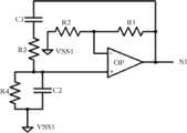
振荡器单元的结构示意图如图3所示,由电阻R1、R2、R3、R4和电容C1、C2和一个放大器OP构成,输出一个与集成变压器单元的特征频率fT频率值相同的正弦波信号。其中R3、C1和R4、C2及R1和R2组成一四臂电桥;C1的一端与R1一端相连,并作为振荡器的输出端,输出信号为S1;C1的另一端与R3相连,R3的另一端与R4和C2的一端相连,并构成放大器OP的正向输入信号,R4的另一端和C2的另一端与地电位VSS1相连;R1的另一端与R2的一端相连,R2的另一端与地电位VSS1相连;S1通过R1、R2进行分压构成放大器OP的反向输入信号;S1通过R1、R2构成的反馈支路对振荡器改善振荡波形,减小放大电路对选频特性的影响并提高振荡电路的带负载能力。The structural diagram of the oscillator unit is shown in Figure 3. It is composed of resistors R1, R2, R3, R4, capacitors C1, C2 and an amplifier OP, and outputs a sine wave signal with the same frequency value as the characteristic frequency fT of the integrated transformer unit. Among them, R3, C1 and R4, C2 and R1 and R2 form a four-arm bridge; one end of C1 is connected to one end of R1, and is used as the output end of the oscillator, and the output signal is S1; the other end of C1 is connected to R3, and R3’s The other end is connected to one end of R4 and C2, and constitutes the positive input signal of the amplifier OP. The other end of R4 and the other end of C2 are connected to the ground potential VSS1; the other end of R1 is connected to one end of R2, and the other end of R2 is connected to The ground potential VSS1 is connected; S1 divides the voltage through R1 and R2 to form the reverse input signal of the amplifier OP; S1 improves the oscillation waveform of the oscillator through the feedback branch formed by R1 and R2, reduces the influence of the amplifier circuit on the frequency selection characteristics and Improve the load capacity of the oscillation circuit.
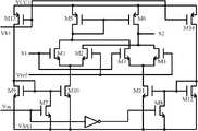
可变增益放大器单元的结构示意图如图4所示,包括PMOS管M5、M6、M13、M14,NMOS管M1、M2、M3、M4、M7、M8、M9、M10、M11、M12。M5、M6、M13、M14的源极与电源电压源VCC1相连,M7、M8、M9、M10、M11、M12的源极接地电位VSS1。M13、M14的栅极相连,接外部偏置信号Vb1,构成电流镜结构;M13的漏极与NMOS管M9、M10的栅极相连,并与M7的漏极相连;M14的漏极与M11、M12的栅极相连,并与M8的漏极相连;M7的栅极接输入电平Vin,M8的栅极接输入电平Vin经过一级反相器后的信号;M9、M12栅漏短接,M10的漏极与差分输入对M1、M2的源极相连,M11的漏极与差分输入对M3、M4的源极相连;M1、M3的漏极与M5的漏极相连,M1、M3的栅极相连;M2、M4的漏极与M6的漏极相连,M2、M4的栅极相连;M5、M6的栅极相连且M5的栅漏短接构成差分输入对M1、M2和M3、M4的电流源负载,M1、M3的栅极接输入信号S1,M2、M4的栅极接外部的作为比较的固定电平Vref。The structural diagram of the variable gain amplifier unit is shown in Figure 4, including PMOS transistors M5, M6, M13, and M14, and NMOS transistors M1, M2, M3, M4, M7, M8, M9, M10, M11, and M12. The sources of M5, M6, M13 and M14 are connected to the power supply voltage source VCC1, and the sources of M7, M8, M9, M10, M11 and M12 are grounded at potential VSS1. The gates of M13 and M14 are connected and connected to the external bias signal Vb1 to form a current mirror structure; the drain of M13 is connected to the gates of NMOS transistors M9 and M10, and is connected to the drain of M7; the drain of M14 is connected to M11, The gate of M12 is connected and connected to the drain of M8; the gate of M7 is connected to the input level Vin, and the gate of M8 is connected to the signal after the input level Vin passes through the first-stage inverter; the gate and drain of M9 and M12 are short-circuited , the drain of M10 is connected to the source of the differential input pair M1, M2, the drain of M11 is connected to the source of the differential input pair M3, M4; the drain of M1, M3 is connected to the drain of M5, and the drain of M1, M3 The gates are connected; the drains of M2 and M4 are connected to the drains of M6, and the gates of M2 and M4 are connected; the gates of M5 and M6 are connected and the gate-drain of M5 is shorted to form a differential input pair M1, M2 and M3, M4 The gates of M1 and M3 are connected to the input signal S1, and the gates of M2 and M4 are connected to an external fixed level Vref for comparison.
这里可变增益放大器单元由两条恒流源支路、有源负载和两对差动输入管构成。M13、M9、M10和M14、M11、M12构成两条恒流源支路,输入电平Vin通过M7和M8分别控制恒流源M9、M10和M11、M12的开关,M7、M8的栅极信号为输入的输入电平Vin和经过一级反相器后的输入电平Vin;M10和M11分别为M1、M2所组成的差分输入对M3、M4组成的差分输入对提供尾电流偏置;M5、M6组成可变增益放大器的有源负载。Here the variable gain amplifier unit is composed of two constant current source branches, an active load and two pairs of differential input transistors. M13, M9, M10 and M14, M11, M12 form two constant current source branches, the input level Vin controls the switches of constant current sources M9, M10 and M11, M12 respectively through M7 and M8, and the gate signals of M7 and M8 M10 and M11 provide tail current bias for the differential input pair M3 and M4 composed of M1 and M2 respectively; M5 , M6 constitutes the active load of the variable gain amplifier.
可变增益放大器单元的工作原理如下:当输入电平Vin为高电平时,M7导通、M8关断,M13、M9、M10组成的恒流源关断,M11、M12、M14组成的恒流源开启,M3、M4组成的差动运放工作,电压增益为Av1;当输入电平Vin为低电平时,M7关断、M8导通,M13、M9、M10组成的恒流源开启,M11、M12、M14组成的恒流源关断,M1、M2组成的差动运放工作,电压增益为Av2,通过调节M13与M14的宽长比得到不同的尾电流,从而得到不同的电压增益。The working principle of the variable gain amplifier unit is as follows: when the input level Vin is high, M7 is turned on, M8 is turned off, the constant current source composed of M13, M9, and M10 is turned off, and the constant current source composed of M11, M12, and M14 is turned off. The source is turned on, the differential operational amplifier composed of M3 and M4 works, and the voltage gain is Av1; when the input level Vin is low, M7 is turned off, M8 is turned on, the constant current source composed of M13, M9, and M10 is turned on, and M11 The constant current source composed of , M12 and M14 is turned off, the differential operational amplifier composed of M1 and M2 works, and the voltage gain is Av2. By adjusting the width-to-length ratio of M13 and M14, different tail currents can be obtained, thereby obtaining different voltage gains.
通过输入电平Vin对振荡器单元所产生的正弦波进行不同增益值的放大,得到一个频率与集成变压器单元特征频率值相同但幅度不同的信号,该信号包含了输入电平Vin的频率信息,该信号与集成变压器的特征频率值相同,可以无失真地通过集成变压器单元进行电平的转换。Through the input level Vin, the sine wave generated by the oscillator unit is amplified with different gain values, and a signal with the same frequency as the characteristic frequency value of the integrated transformer unit but different amplitude is obtained. The signal contains the frequency information of the input level Vin, This signal is the same as the characteristic frequency value of the integrated transformer, and can be converted through the integrated transformer unit without distortion.
普通放大器单元的结构示意图如图5所示,采用折叠式共源共栅放大器结构,包括:PMOS管M28、M29、M30、M31、M37,NMOS管M24、M25、M26、M27、M32、M33、M34、M35、M36。具体电路的连接关系为:M28、M29、M37的源极接外部电源电压源VCC2,M26、M27、M34、M35、M36的源极接地电位VSS2。M26、M27的栅极接在一起,M27栅漏短接且接到恒流源Iref1,M26的漏极与差分输入对M24、M25的源极相连,M24的栅极接输入信号S3,M25的栅极与外部的比较的固定电平Vref相连;M28、M29、M37的栅极相连,M37栅漏短接且接到恒流源Iref2;M28的漏极与M24的漏极、M30的源极相连,M29的漏极与M25的漏极、M31的源极相连;M30、M31的栅极短接且接到外部偏置信号Vb2;M30的漏极与M32的漏极接信号S3,M31的漏极和M33的漏极分别与外部的作为比较的固定电平Vref相连(对应的图5已修改),M32、M33的栅极相连且接到外部偏置信号Vb3;M32的源极与M34的漏极相连,M33的源极与M35的漏极相连;M34、M35、M36的栅极接到一起,M36栅漏短接且接到恒流源Iref3。The schematic diagram of the common amplifier unit structure is shown in Figure 5, which adopts a folded cascode amplifier structure, including: PMOS tubes M28, M29, M30, M31, M37, NMOS tubes M24, M25, M26, M27, M32, M33, M34, M35, M36. The connection relationship of the specific circuit is: the sources of M28, M29 and M37 are connected to the external power supply voltage source VCC2, and the sources of M26, M27, M34, M35 and M36 are connected to the ground potential VSS2. The gates of M26 and M27 are connected together, the gate-drain of M27 is short-circuited and connected to the constant current source Iref1, the drain of M26 is connected to the source of the differential input pair M24 and M25, the gate of M24 is connected to the input signal S3, and the gate of M25 The gate is connected to the external comparative fixed level Vref; the gates of M28, M29, and M37 are connected, and the gate-drain of M37 is short-circuited and connected to the constant current source Iref2; the drain of M28 is connected to the drain of M24 and the source of M30 The drain of M29 is connected to the drain of M25 and the source of M31; the gates of M30 and M31 are short-circuited and connected to the external bias signal Vb2; the drain of M30 and the drain of M32 are connected to the signal S3, and the drain of M31 The drain and the drain of M33 are respectively connected to the external fixed level Vref as a comparison (the corresponding figure 5 has been modified), the gates of M32 and M33 are connected and connected to the external bias signal Vb3; the source of M32 is connected to the M34 The drain of M33 is connected to the drain of M35; the gates of M34, M35, and M36 are connected together, and the gate-drain of M36 is short-circuited and connected to the constant current source Iref3.
检波单元的结构示意图如图6所示,检波单元可以使用并联型二极管包络检波电路,也可以使用串联型二极管包络检波电路。The structural schematic diagram of the detection unit is shown in FIG. 6 , and the detection unit may use a parallel diode envelope detection circuit or a series diode envelope detection circuit.
并联型二极管包络检波电路如图6(a),包括大电容C3、电阻R5和二极管D1,这里的大电容指的是钽电容、电解电容等具有极性的电容。串联型二极管包络检波电路如图6(b),包括电容C4、电阻R6和二极管D2。The parallel diode envelope detection circuit is shown in Figure 6(a), including a large capacitor C3, a resistor R5, and a diode D1. The large capacitor here refers to polarized capacitors such as tantalum capacitors and electrolytic capacitors. The series diode envelope detection circuit is shown in Figure 6(b), including capacitor C4, resistor R6 and diode D2.
图6(a)的具体连接关系为:大电容C3的正极板接普通放大器单元的输出信号S4,C3的负极板与电阻R5和二极管D1的阳极相连,并作为输出信号S5的输出端;R5的另一端和D1的阴极、参考地电位VSS2相连。The specific connection relationship of Fig. 6 (a) is: the positive plate of the large capacitor C3 is connected to the output signal S4 of the ordinary amplifier unit, the negative plate of C3 is connected with the anode of the resistor R5 and the diode D1, and is used as the output terminal of the output signal S5; R5 The other end of D1 is connected to the cathode of D1 and the reference ground potential VSS2.
图6(b)的具体连接关系为:D2的阳极与普通放大器单元的输出信号S4相连,D2的阴极与电阻R6、电容C4的一端相连,且作为输出信号S5的输出端;R6的另一端与C4的另一端、参考地电位VSS2相连。The specific connection relationship in Figure 6(b) is: the anode of D2 is connected to the output signal S4 of the ordinary amplifier unit, the cathode of D2 is connected to one end of the resistor R6 and capacitor C4, and is used as the output end of the output signal S5; the other end of R6 Connect with the other end of C4 and the reference ground potential VSS2.
比较器单元的结构示意图如图7所示,包括PMOS管M17、M18、M22、M23和NMOS管M15、M16、M19、M20、M21。具体连接关系为:PMOS管M17、M18、M22、M23的源极均接电源电压源VCC2,M19、M20、M21的源极均接地电位VSS2。M22的栅极接外部偏置信号Vb4,漏极接M19、M20、M21的栅极,M19栅漏短接,与M20、M21组成电流镜结构,为运放提供尾电流;M20的漏极接运放的差分输入对M15、M16的源极,M15的栅极接输入信号S5,M16的栅极接作为比较的固定电平Vref,M15的漏极接M17、M18的栅极,M17栅漏短接,M17、M18构成比较器的有源负载,M18的漏极与M16的漏极和M23的栅极相连,作为比较器的第一级输出;M23的漏极与M21的漏极相连,并作为两级比较器的输出端,输出信号为Vout。The structural diagram of the comparator unit is shown in FIG. 7 , including PMOS transistors M17, M18, M22, M23 and NMOS transistors M15, M16, M19, M20, M21. The specific connection relationship is: the sources of the PMOS transistors M17, M18, M22, and M23 are all connected to the power supply voltage source VCC2, and the sources of the M19, M20, and M21 are all connected to the ground potential VSS2. The gate of M22 is connected to the external bias signal Vb4, and the drain is connected to the gates of M19, M20, and M21. The differential input pair of the operational amplifier is connected to the source of M15 and M16, the gate of M15 is connected to the input signal S5, the gate of M16 is connected to the fixed level Vref as a comparison, the drain of M15 is connected to the gate of M17 and M18, and the gate of M17 is drained Short circuit, M17, M18 constitute the active load of the comparator, the drain of M18 is connected with the drain of M16 and the gate of M23, as the first stage output of the comparator; the drain of M23 is connected with the drain of M21, And as the output terminal of the two-stage comparator, the output signal is Vout.
下面结合图8说明本发明实施例的工作原理:The working principle of the embodiment of the present invention is illustrated below in conjunction with FIG. 8:
振荡器单元用来产生一个与集成变压器单元的特征频率fT频率值相同的正弦波信号S1,一般说来S1的频率远高于输入电平Vin的频率;输入电平Vin作为可变增益放大器单元的尾电流的控制信号,振荡器单元的输出信号S1作为可变增益放大器单元的输入信号,通过输入电平Vin的控制,得到一个载波信号S2;S2信号频率与S1信号相同,即与集成变压器单元特征频率fT频率相同,因此它可以无失真地通过集成变压器单元,得到信号S3。集成变压器单元负载端的回路电阻R,使得集成变压器单元负载端形成一个完整的回路而正常工作,但经过的信号可能会衰减。为了使检波单元的包络更宽而有利于检波,将S3信号进行放大,得到信号S4。S4信号经过包络检波电路后可以将输入的输入电平Vin的频率特性检波出来得到信号S5,再通过比较器单元进行整形后得到输出信号Vout。Vout信号的频率特性与输入端的输入电平Vin相同。由于集成变压器单元初级端的参考地电位为VSS1,次级端的参考地电位为VSS2,因此Vout波形中的低电压部分的电平位移幅度,由这两个地电位的相对电位来确定。而Vout波形中的高电压部分的电平位移幅度,由集成变压器单元次级端电路的电源电位决定。The oscillator unit is used to generate a sine wave signal S1 with the same frequency value as the characteristic frequency fT of the integrated transformer unit. Generally speaking, the frequency of S1 is much higher than the frequency of the input level Vin; the input level Vin is used as a variable gain amplifier The control signal of the tail current of the unit, the output signal S1 of the oscillator unit is used as the input signal of the variable gain amplifier unit, and a carrier signal S2 is obtained through the control of the input level Vin; the frequency of the S2 signal is the same as that of the S1 signal, that is, the integrated The characteristic frequency fT of the transformer unit is the same frequency, so it can pass through the integrated transformer unit without distortion to obtain the signal S3. The loop resistance R at the load end of the integrated transformer unit makes the load end of the integrated transformer unit form a complete loop and work normally, but the passing signal may be attenuated. In order to make the envelope of the detection unit wider and facilitate detection, the S3 signal is amplified to obtain the signal S4. After the S4 signal passes through the envelope detection circuit, the frequency characteristic of the input level Vin can be detected to obtain the signal S5, and then the output signal Vout is obtained after being shaped by the comparator unit. The frequency characteristic of the Vout signal is the same as the input level Vin at the input terminal. Since the reference ground potential of the primary side of the integrated transformer unit is VSS1, and the reference ground potential of the secondary side is VSS2, the magnitude of the level shift of the low voltage part of the Vout waveform is determined by the relative potential of the two ground potentials. The level shift amplitude of the high voltage part in the Vout waveform is determined by the power supply potential of the secondary end circuit of the integrated transformer unit.
可以看出,本发明通过集成变压器单元实现电平位移电路,可实现输入电压信号的整体电平位移,即输入电压信号的高电平电位和低电平电位一起位移相同的幅度;同时由于集成变压器单元良好的隔离特性,保证了该电平位移电路中高低压电路的隔离性很好,解决了现有的电平位移电路设计中隔离比较困难的问题。通过集成变压器单元的隔离性,使输入电压信号的整体位移幅度可以特别大,并且这种电压信号的整体电平位移既可以是往正电压方向的电平位移,也可以是往负电压方向的电平位移;如果对于输入电压信号的相对幅度值(即输入电压信号的高电平值减去低电平值)不需要做电平位移的话,集成变压器次级电路部分的地电位相对于初级电路部分的地电位可以是一个电压值相差很大的电位,次级电路的工作电压但两部分相对于彼此地电位的电源的幅度可以是相同的,因此即使电平位移的电压变换幅度很大,但两部分电路所使用的器件对耐压的要求是相同的,都可采用低压器件来实现,避免了对高压器件的要求;同时这种方案借助了载波的概念,使得由振荡器产生的特定频率的信号,而不是由低频的电压输入信号,通过集成变压器进行变换,从而很好解决了集成变压器由于制造工艺的限制不能通过低频电压信号的缺点,使得各种频率的低频电压控制信号都能够进行电平位移。It can be seen that the present invention realizes the level displacement circuit through the integrated transformer unit, which can realize the overall level displacement of the input voltage signal, that is, the high-level potential and the low-level potential of the input voltage signal are displaced by the same amplitude; at the same time, due to the integrated The good isolation characteristic of the transformer unit ensures good isolation of the high and low voltage circuits in the level shifting circuit, and solves the difficult problem of isolation in the existing level shifting circuit design. By integrating the isolation of the transformer unit, the overall displacement of the input voltage signal can be particularly large, and the overall level displacement of this voltage signal can be either a level displacement in the positive voltage direction or a negative voltage direction. Level shift; if no level shift is required for the relative amplitude value of the input voltage signal (that is, the high level value of the input voltage signal minus the low level value), the ground potential of the secondary circuit part of the integrated transformer is relative to the primary The ground potential of the circuit part can be a potential with a large difference in voltage value, the operating voltage of the secondary circuit, but the magnitude of the power supply of the two parts relative to each other's ground potential can be the same, so even if the voltage change range of the level shift is large , but the devices used in the two parts of the circuit have the same requirements for withstand voltage, and both can be realized by using low-voltage devices, avoiding the requirements for high-voltage devices; at the same time, this scheme uses the concept of carrier wave to make the vibration generated by the oscillator The signal of a specific frequency, instead of the low-frequency voltage input signal, is transformed by the integrated transformer, which solves the problem that the integrated transformer cannot pass the low-frequency voltage signal due to the limitation of the manufacturing process, so that the low-frequency voltage control signals of various frequencies are all Capable of level shifting.
本发明所述的基于集成变压器的高压电平位移电路系统,是一个能对输入控制电压信号进行无失真的电平位移,同时又能很好地应用于高压环境的电路系统。同时由于集成变压器良好的隔离特性,所以该电路系统中高低压电路的隔离性很好,因此它可以作为半导体集成电路高压功率电子芯片中基本的电平位移电路。The high-voltage level shifting circuit system based on the integrated transformer of the present invention is a circuit system capable of level shifting the input control voltage signal without distortion, and at the same time can be well applied in a high-voltage environment. At the same time, due to the good isolation characteristics of the integrated transformer, the isolation of the high and low voltage circuits in the circuit system is very good, so it can be used as the basic level shift circuit in the high voltage power electronic chip of the semiconductor integrated circuit.
本领域的普通技术人员将会意识到,这里所述的实施例是为了帮助读者理解本发明的原理,应被理解为本发明的保护范围并不局限于这样的特别陈述和实施例。本领域的普通技术人员可以根据本发明公开的这些技术启示做出各种不脱离本发明实质的其它各种具体变形和组合,这些变形和组合仍然在本发明的保护范围内。Those skilled in the art will appreciate that the embodiments described here are to help readers understand the principles of the present invention, and it should be understood that the protection scope of the present invention is not limited to such specific statements and embodiments. Those skilled in the art can make various other specific modifications and combinations based on the technical revelations disclosed in the present invention without departing from the essence of the present invention, and these modifications and combinations are still within the protection scope of the present invention.
Claims (5)
Priority Applications (1)
| Application Number | Priority Date | Filing Date | Title |
|---|---|---|---|
| CN201110066729ACN102176672B (en) | 2011-03-18 | 2011-03-18 | Level shifting circuit |
Applications Claiming Priority (1)
| Application Number | Priority Date | Filing Date | Title |
|---|---|---|---|
| CN201110066729ACN102176672B (en) | 2011-03-18 | 2011-03-18 | Level shifting circuit |
Publications (2)
| Publication Number | Publication Date |
|---|---|
| CN102176672Atrue CN102176672A (en) | 2011-09-07 |
| CN102176672B CN102176672B (en) | 2012-09-12 |
Family
ID=44519781
Family Applications (1)
| Application Number | Title | Priority Date | Filing Date |
|---|---|---|---|
| CN201110066729AExpired - Fee RelatedCN102176672B (en) | 2011-03-18 | 2011-03-18 | Level shifting circuit |
Country Status (1)
| Country | Link |
|---|---|
| CN (1) | CN102176672B (en) |
Cited By (2)
| Publication number | Priority date | Publication date | Assignee | Title |
|---|---|---|---|---|
| CN102394627A (en)* | 2011-09-28 | 2012-03-28 | 电子科技大学 | High Voltage Level Shift Circuit Based on Integrated Capacitor |
| CN106896858A (en)* | 2017-03-17 | 2017-06-27 | 厦门思力科电子科技有限公司 | A kind of circuit for designing common-mode voltage |
Citations (5)
| Publication number | Priority date | Publication date | Assignee | Title |
|---|---|---|---|---|
| US5533054A (en)* | 1993-07-09 | 1996-07-02 | Technitrol, Inc. | Multi-level data transmitter |
| US6122180A (en)* | 1998-12-18 | 2000-09-19 | Fairfield Korea Semiconductor Ltd. | SMPS with constant power control circuit |
| CN101090256A (en)* | 2006-06-13 | 2007-12-19 | 美国芯源系统股份有限公司 | High-impedance level-shifting amplifier |
| CN101697454A (en)* | 2009-10-30 | 2010-04-21 | 北京航星力源科技有限公司 | Grid drive circuit of insulated grid device |
| CN101820272A (en)* | 2009-02-27 | 2010-09-01 | 恩益禧电子股份有限公司 | Level shifting circuit and switching circuit including the level shifting circuit |
- 2011
- 2011-03-18CNCN201110066729Apatent/CN102176672B/ennot_activeExpired - Fee Related
Patent Citations (5)
| Publication number | Priority date | Publication date | Assignee | Title |
|---|---|---|---|---|
| US5533054A (en)* | 1993-07-09 | 1996-07-02 | Technitrol, Inc. | Multi-level data transmitter |
| US6122180A (en)* | 1998-12-18 | 2000-09-19 | Fairfield Korea Semiconductor Ltd. | SMPS with constant power control circuit |
| CN101090256A (en)* | 2006-06-13 | 2007-12-19 | 美国芯源系统股份有限公司 | High-impedance level-shifting amplifier |
| CN101820272A (en)* | 2009-02-27 | 2010-09-01 | 恩益禧电子股份有限公司 | Level shifting circuit and switching circuit including the level shifting circuit |
| CN101697454A (en)* | 2009-10-30 | 2010-04-21 | 北京航星力源科技有限公司 | Grid drive circuit of insulated grid device |
Cited By (2)
| Publication number | Priority date | Publication date | Assignee | Title |
|---|---|---|---|---|
| CN102394627A (en)* | 2011-09-28 | 2012-03-28 | 电子科技大学 | High Voltage Level Shift Circuit Based on Integrated Capacitor |
| CN106896858A (en)* | 2017-03-17 | 2017-06-27 | 厦门思力科电子科技有限公司 | A kind of circuit for designing common-mode voltage |
Also Published As
| Publication number | Publication date |
|---|---|
| CN102176672B (en) | 2012-09-12 |
Similar Documents
| Publication | Publication Date | Title |
|---|---|---|
| US5594383A (en) | Analog filter circuit and semiconductor integrated circuit device using the same | |
| US8427122B2 (en) | Enhancement of power supply rejection for operational amplifiers and voltage regulators | |
| CN113726298A (en) | Fully-differential two-stage operational amplifier circuit | |
| CN114710124B (en) | Rail-to-rail input-output operational transconductance amplifier based on low ripple charge pump | |
| CN101800519B (en) | Operational amplifier and method for reducing offset voltage of operational amplifier | |
| TWI487262B (en) | Voltage to current converting circuit | |
| CN109672418A (en) | A kind of high gain operational amplifier using feedforward compensation | |
| CN108712800A (en) | N bit digital calibration errors amplifying circuit, LED drive circuit and its error amplify offset compensation method | |
| JP2004320712A (en) | Amplifier circuit | |
| CN102176672B (en) | Level shifting circuit | |
| CN107834986A (en) | Single-stage AB classes operation transconductance amplifier and analog circuit | |
| CN107968635A (en) | Electric current reclaiming type amplifier and analog circuit | |
| EP4388656A1 (en) | Class-d amplifier with deadtime distortion compensation | |
| CN114826175A (en) | Power amplifying circuit | |
| JP5456896B2 (en) | Switching amplifier circuit configuration and switching amplification method | |
| CN103414329A (en) | Voltage peak value locking circuit | |
| CN114938129B (en) | An Adaptive High Linearity Slope Compensation Circuit | |
| CN111654244A (en) | A High Linearity GΩ Class Equivalent Resistance Circuit with PVT Robustness | |
| CN113676159B (en) | Oscillator, chip and electronic equipment | |
| CN114614671B (en) | Power supply suitable for 5GNR broadband high-efficiency envelope tracking power amplifier | |
| JP4624221B2 (en) | Differential operational amplifier | |
| CN101902208A (en) | Operational amplification circuit | |
| CN114077272B (en) | Radio frequency power rectifier circuit | |
| JP2004180268A (en) | Amplifier circuit and liquid crystal display device using the same | |
| CN118100812B (en) | Amplitude limiting amplifying circuit for radio frequency integrated chip |
Legal Events
| Date | Code | Title | Description |
|---|---|---|---|
| C06 | Publication | ||
| PB01 | Publication | ||
| C10 | Entry into substantive examination | ||
| SE01 | Entry into force of request for substantive examination | ||
| C14 | Grant of patent or utility model | ||
| GR01 | Patent grant | ||
| CF01 | Termination of patent right due to non-payment of annual fee | Granted publication date:20120912 Termination date:20150318 | |
| EXPY | Termination of patent right or utility model |