CN102174676A - Preparation method for stannum, indium and stibium series lead-free solder tinning copper strip used for solar battery - Google Patents
Preparation method for stannum, indium and stibium series lead-free solder tinning copper strip used for solar batteryDownload PDFInfo
- Publication number
- CN102174676A CN102174676ACN2011100302864ACN201110030286ACN102174676ACN 102174676 ACN102174676 ACN 102174676ACN 2011100302864 ACN2011100302864 ACN 2011100302864ACN 201110030286 ACN201110030286 ACN 201110030286ACN 102174676 ACN102174676 ACN 102174676A
- Authority
- CN
- China
- Prior art keywords
- tin
- antimony
- copper
- indium
- silver
- Prior art date
- Legal status (The legal status is an assumption and is not a legal conclusion. Google has not performed a legal analysis and makes no representation as to the accuracy of the status listed.)
- Pending
Links
- 229910000679solderInorganic materials0.000titleclaimsabstractdescription64
- RYGMFSIKBFXOCR-UHFFFAOYSA-NCopperChemical compound[Cu]RYGMFSIKBFXOCR-UHFFFAOYSA-N0.000titleclaimsabstractdescription50
- 229910052802copperInorganic materials0.000titleclaimsabstractdescription46
- 239000010949copperSubstances0.000titleclaimsabstractdescription46
- ATJFFYVFTNAWJD-UHFFFAOYSA-NTinChemical compound[Sn]ATJFFYVFTNAWJD-UHFFFAOYSA-N0.000titleclaimsabstractdescription31
- 229910052738indiumInorganic materials0.000titleclaimsabstractdescription24
- APFVFJFRJDLVQX-UHFFFAOYSA-Nindium atomChemical compound[In]APFVFJFRJDLVQX-UHFFFAOYSA-N0.000titleclaimsabstractdescription21
- 238000002360preparation methodMethods0.000titleclaimsabstractdescription7
- 229910045601alloyInorganic materials0.000claimsabstractdescription63
- 239000000956alloySubstances0.000claimsabstractdescription63
- 229910052787antimonyInorganic materials0.000claimsabstractdescription32
- 229910052718tinInorganic materials0.000claimsabstractdescription32
- 239000011135tinSubstances0.000claimsabstractdescription31
- WATWJIUSRGPENY-UHFFFAOYSA-Nantimony atomChemical compound[Sb]WATWJIUSRGPENY-UHFFFAOYSA-N0.000claimsabstractdescription24
- 229910052709silverInorganic materials0.000claimsabstractdescription18
- 239000004332silverSubstances0.000claimsabstractdescription17
- BQCADISMDOOEFD-UHFFFAOYSA-NSilverChemical compound[Ag]BQCADISMDOOEFD-UHFFFAOYSA-N0.000claimsabstractdescription16
- 229910052797bismuthInorganic materials0.000claimsabstractdescription7
- JCXGWMGPZLAOME-UHFFFAOYSA-Nbismuth atomChemical compound[Bi]JCXGWMGPZLAOME-UHFFFAOYSA-N0.000claimsabstractdescription7
- 238000003466weldingMethods0.000claimsabstractdescription6
- BRMNETVQNQAIKC-UHFFFAOYSA-N[Sn].[In].[Sb]Chemical class[Sn].[In].[Sb]BRMNETVQNQAIKC-UHFFFAOYSA-N0.000claimsabstractdescription5
- 238000005303weighingMethods0.000claimsabstractdescription3
- 238000002844meltingMethods0.000claimsdescription23
- 230000008018meltingEffects0.000claimsdescription23
- 238000007747platingMethods0.000claimsdescription11
- 238000007598dipping methodMethods0.000claimsdescription3
- 238000007654immersionMethods0.000claimsdescription2
- 239000000203mixtureSubstances0.000claimsdescription2
- NTSDHVIXFWZYSM-UHFFFAOYSA-N[Ag].[Sb].[Sn]Chemical group[Ag].[Sb].[Sn]NTSDHVIXFWZYSM-UHFFFAOYSA-N0.000claims1
- 239000000470constituentSubstances0.000claims1
- 238000000034methodMethods0.000abstractdescription13
- 238000003723SmeltingMethods0.000abstractdescription5
- XUFUDVIAKKOUOK-UHFFFAOYSA-N[Cu].[Sb].[Ag].[Sn]Chemical compound[Cu].[Sb].[Ag].[Sn]XUFUDVIAKKOUOK-UHFFFAOYSA-N0.000abstractdescription4
- 238000003756stirringMethods0.000abstractdescription3
- 238000004519manufacturing processMethods0.000description10
- 239000002245particleSubstances0.000description10
- WPYVAWXEWQSOGY-UHFFFAOYSA-Nindium antimonideChemical compound[Sb]#[In]WPYVAWXEWQSOGY-UHFFFAOYSA-N0.000description7
- 239000011159matrix materialSubstances0.000description7
- GVFOJDIFWSDNOY-UHFFFAOYSA-Nantimony tinChemical compound[Sn].[Sb]GVFOJDIFWSDNOY-UHFFFAOYSA-N0.000description6
- 239000011248coating agentSubstances0.000description5
- 238000000576coating methodMethods0.000description5
- 229910000765intermetallicInorganic materials0.000description5
- 239000000463materialSubstances0.000description5
- 229910020816Sn PbInorganic materials0.000description4
- 229910020922Sn-PbInorganic materials0.000description4
- 229910008783Sn—PbInorganic materials0.000description4
- 238000005260corrosionMethods0.000description4
- 230000007797corrosionEffects0.000description4
- 238000005476solderingMethods0.000description4
- 229910006640β-SnInorganic materials0.000description4
- 229910006632β—SnInorganic materials0.000description4
- 229910017482Cu 6 Sn 5Inorganic materials0.000description3
- 229910017944Ag—CuInorganic materials0.000description2
- VEXZGXHMUGYJMC-UHFFFAOYSA-NHydrochloric acidChemical compoundClVEXZGXHMUGYJMC-UHFFFAOYSA-N0.000description2
- OAICVXFJPJFONN-UHFFFAOYSA-NPhosphorusChemical compound[P]OAICVXFJPJFONN-UHFFFAOYSA-N0.000description2
- 230000007423decreaseEffects0.000description2
- 238000009713electroplatingMethods0.000description2
- 238000003912environmental pollutionMethods0.000description2
- 230000007774longtermEffects0.000description2
- 229910052698phosphorusInorganic materials0.000description2
- 239000011574phosphorusSubstances0.000description2
- -1tin-indium-bismuth-aluminum-phosphorusChemical compound0.000description2
- XLYOFNOQVPJJNP-UHFFFAOYSA-NwaterSubstancesOXLYOFNOQVPJJNP-UHFFFAOYSA-N0.000description2
- 229910001245Sb alloyInorganic materials0.000description1
- HCHKCACWOHOZIP-UHFFFAOYSA-NZincChemical compound[Zn]HCHKCACWOHOZIP-UHFFFAOYSA-N0.000description1
- 229910052782aluminiumInorganic materials0.000description1
- XAGFODPZIPBFFR-UHFFFAOYSA-NaluminiumChemical compound[Al]XAGFODPZIPBFFR-UHFFFAOYSA-N0.000description1
- 238000004140cleaningMethods0.000description1
- 239000003245coalSubstances0.000description1
- 238000001035dryingMethods0.000description1
- 230000005611electricityEffects0.000description1
- 238000005265energy consumptionMethods0.000description1
- 238000005516engineering processMethods0.000description1
- 230000004907fluxEffects0.000description1
- 239000012535impuritySubstances0.000description1
- 230000002427irreversible effectEffects0.000description1
- 239000007788liquidSubstances0.000description1
- 238000010309melting processMethods0.000description1
- 231100000252nontoxicToxicity0.000description1
- 230000003000nontoxic effectEffects0.000description1
- 239000005022packaging materialSubstances0.000description1
- 238000004806packaging method and processMethods0.000description1
- 238000005554picklingMethods0.000description1
- 238000010248power generationMethods0.000description1
- 238000001556precipitationMethods0.000description1
- 230000001360synchronised effectEffects0.000description1
- 238000005406washingMethods0.000description1
- 239000002699waste materialSubstances0.000description1
- 229910052725zincInorganic materials0.000description1
- 239000011701zincSubstances0.000description1
Images


Classifications
- Y—GENERAL TAGGING OF NEW TECHNOLOGICAL DEVELOPMENTS; GENERAL TAGGING OF CROSS-SECTIONAL TECHNOLOGIES SPANNING OVER SEVERAL SECTIONS OF THE IPC; TECHNICAL SUBJECTS COVERED BY FORMER USPC CROSS-REFERENCE ART COLLECTIONS [XRACs] AND DIGESTS
- Y02—TECHNOLOGIES OR APPLICATIONS FOR MITIGATION OR ADAPTATION AGAINST CLIMATE CHANGE
- Y02P—CLIMATE CHANGE MITIGATION TECHNOLOGIES IN THE PRODUCTION OR PROCESSING OF GOODS
- Y02P70/00—Climate change mitigation technologies in the production process for final industrial or consumer products
- Y02P70/50—Manufacturing or production processes characterised by the final manufactured product
Landscapes
- Coating With Molten Metal (AREA)
Abstract
Translated fromChinese
Description
Translated fromChinese技术领域technical field
本发明属于电子工业基础材料领域,特别涉及一种无铅焊料及其镀锡铜丝或铜带的制备方法。The invention belongs to the field of basic materials in the electronic industry, in particular to a preparation method of lead-free solder and tinned copper wire or copper strip.
背景技术Background technique
当电力、煤炭、石油等不可再生能源频频告急,能源问题日益成为制约国际社会经济发展的瓶颈时,越来越多的国家开始实行“阳光计划”,开发太阳能资源,寻求经济发展的新动力。可以说,太阳能是取之不尽的清洁能源。目前把太阳能转化为电能的主要方式是太阳能电池,太阳能电池能够保证经济与环境的双赢,而且比风力发电制约条件少,人类也许在可以预期的未来,在更大范围内用太阳能电池取代化石能源,彻底解决人类的能源问题。无铅焊料作为太阳能电池封装的主要材料之一,除了实现各个组件的连接之外,更重要的是在汇流带和互连条中的应用,汇流带和互连条镀锡用无铅焊料,对于其载流能力及其他性能影响很大。Sn-Pb钎料在各方面的优越性,使其成为过去太阳能电池领域广泛使用的封装材料,但鉴于铅的危害,目前全球许多国家和组织都通过立法限制其使用,应该看到无铅化已成为电子制造锡焊技术不可逆转的潮流。经过多年努力,目前中国电子组装无铅化比率已经达到70%以上。然而目前市场上的无铅焊料虽能满足无毒害、环保的行业基本要求,但全面取代传统焊料也面临很大挑战。When non-renewable energy sources such as electricity, coal, and oil are running out frequently, and energy issues have increasingly become a bottleneck restricting the development of the international society and economy, more and more countries have begun to implement the "Sunshine Plan" to develop solar energy resources and seek new impetus for economic development. It can be said that solar energy is an inexhaustible clean energy. At present, the main way to convert solar energy into electrical energy is solar cells. Solar cells can ensure a win-win situation for the economy and the environment, and there are fewer constraints than wind power generation. Humans may use solar cells to replace fossil energy on a larger scale in the foreseeable future. , completely solve the human energy problem. Lead-free solder is one of the main materials for solar cell packaging. In addition to realizing the connection of various components, more importantly, it is used in bus strips and interconnection strips. Lead-free solder is used for tinning of bus strips and interconnection strips. It has a great influence on its current carrying capacity and other properties. The superiority of Sn-Pb solder in all aspects made it a widely used packaging material in the field of solar cells in the past. However, in view of the hazards of lead, many countries and organizations around the world have passed legislation to restrict its use. Lead-free should be seen It has become an irreversible trend in electronic manufacturing soldering technology. After years of hard work, the lead-free rate of electronic assembly in China has reached over 70%. However, although the lead-free solder currently on the market can meet the basic requirements of the non-toxic and environmentally friendly industry, it is still facing great challenges to completely replace traditional solder.
目前各国研究的焦点都集中于Sn-Ag-Cu合金,优良的性能使其成为目前最被看好的用以替代Sn-37Pb焊料的无铅焊料。但是Sn-Ag-Cu合金具有较高的Ag含量,而银的高价格直接导致了焊料生产成本的增加,产品竞争力下降。另一方面无铅焊料的焊接工艺较传统含铅焊料差,这些无铅焊料的熔点多数在210℃以上,远高于传统含铅焊料,对被焊材料和焊接设备要求高。这些因素制约着无铅焊料的进一步发展和应用。因此研发成本低、性能与应用环境匹配更好的低银第二代无铅焊料成为无铅焊料发展的必然趋势和研发热点之一。At present, the focus of research in various countries is on Sn-Ag-Cu alloy, and its excellent performance makes it the most promising lead-free solder to replace Sn-37Pb solder. However, the Sn-Ag-Cu alloy has a relatively high Ag content, and the high price of silver directly leads to an increase in solder production costs and a decline in product competitiveness. On the other hand, the soldering process of lead-free solder is worse than that of traditional lead-containing solder. The melting point of these lead-free solders is mostly above 210°C, which is much higher than that of traditional lead-containing solder, and has high requirements for soldered materials and welding equipment. These factors restrict the further development and application of lead-free solder. Therefore, the low-silver second-generation lead-free solder with low R&D cost and better performance matching with the application environment has become an inevitable trend in the development of lead-free solder and one of the R&D hotspots.
镀锡铜丝或铜带是电子工业的一种基础材料,太阳能电池组件中,汇流带及互连条一般均为镀锡铜带。镀锡铜带的生产工艺有两种传统工艺,一种是电镀工艺,一种是热浸工艺,采用无铅焊料合金进行。而电镀工艺由于耗能大,对环境污染严重,废液处理成本高,应用不多。热浸工艺成本低,节能对环境污染小。Tinned copper wire or copper strip is a basic material in the electronics industry. In solar cell modules, busbars and interconnection strips are generally tinned copper strips. There are two traditional processes for the production of tinned copper strip, one is the electroplating process, and the other is the hot dip process, which is carried out with lead-free solder alloys. The electroplating process is not widely used due to its high energy consumption, serious environmental pollution, and high cost of waste liquid treatment. The cost of the hot dipping process is low, and the energy saving has little environmental pollution.
发明内容Contents of the invention
本发明目的是提供低成本高性能的锡铟锑系无铅焊料,满足太阳能电池汇流带和互连条热浸镀锡的要求。汇流带的选用主要是依据其载流能力,要求焊料具有良好的可焊性和焊接可靠性,抗腐蚀性能好,在与太阳能电池使用同步的环境下长期工作不会脱落,镀层需保证汇流带和互连条的优良的导电性和加工延展性,镀层均匀,尤其重要的是焊料该焊料由于银含量较低所以降低了生产成本,但其性能仍可满足工业应用要求,其制备方法简单。The purpose of the invention is to provide low-cost and high-performance tin-indium-antimony-based lead-free solder to meet the requirements of hot-dip tinning of solar cell busbars and interconnection strips. The selection of the busbar is mainly based on its current-carrying capacity. The solder is required to have good solderability and welding reliability, good corrosion resistance, and it will not fall off for a long time in an environment that is synchronized with the use of solar cells. The coating must ensure that the busbar And the excellent electrical conductivity and processing ductility of the interconnection strip, the uniform coating, and especially the solder, which reduces the production cost due to its low silver content, but its performance can still meet the requirements of industrial applications, and its preparation method is simple.
本发明提供一种无铅焊料合金的镀锡铜带,是以锡为基料添加重量百分比为0.5-1.5的铟、0.7-2.5的锑形成锡铟锑系无铅焊料,采用热浸镀方式镀在铜带的表面上,制成无铅焊料合金镀锡铜带。The invention provides a tin-plated copper strip of a lead-free solder alloy, which uses tin as a base material to add 0.5-1.5 weight percent of indium and 0.7-2.5 weight percent of antimony to form tin-indium-antimony-based lead-free solder, and adopts a hot-dip plating method Plated on the surface of copper strip to make lead-free solder alloy tinned copper strip.
本发明的技术方案如下:Technical scheme of the present invention is as follows:
太阳能电池用锡铟锑系无铅焊料镀锡铜丝或铜带的制备方法,其特征是将纯锡、铟、锑及铋、铜、银按质量比为83~99∶0.5~9∶0.1~8∶0~4∶0~1∶0~1进行称量,首先将锑、铜和银与锡按1∶10在熔炼炉中熔化并搅拌,使锑、铜和银完全熔化在锡里,形成锡锑银铜中间合金;然后将剩余的锡与其他组元一起熔炼并形成相应的中间合金;最后将两种中间合金一起熔炼并搅拌,使其均匀混合;然后再应用传统的热浸焊工艺,将无铅焊料合金浸镀在铜丝或铜带上。A method for preparing tin-indium-antimony lead-free solder tinned copper wire or copper strip for solar cells, characterized in that pure tin, indium, antimony, bismuth, copper, and silver are mixed in a mass ratio of 83-99:0.5-9:0.1 ~8:0~4:0~1:0~1 for weighing, first melt antimony, copper, silver and tin in a smelting furnace at a ratio of 1:1 and stir, so that antimony, copper and silver are completely melted in tin , to form a tin-antimony-silver-copper master alloy; then the remaining tin is smelted together with other components to form a corresponding master alloy; finally, the two master alloys are melted together and stirred to make them evenly mixed; and then traditional hot dipping is applied Soldering process in which lead-free solder alloys are dip-plated on copper wire or strip.
所述的锑优选质量比为0.7~2.5.The preferred mass ratio of described antimony is 0.7~2.5.
所述的铟优选质量比为0.5~1.5.The preferable mass ratio of described indium is 0.5~1.5.
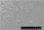
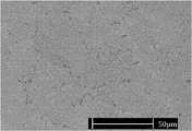
采用传统的热浸焊工艺,将无铅焊料合金浸镀在铜带上。其中传统热浸镀工艺流程如图1所示,部分成分的无铅焊料背散射照片如图2-6所示。The lead-free solder alloy is dip-plated on the copper strip using the conventional hot-dip soldering process. The traditional hot-dip plating process flow is shown in Figure 1, and the backscattered photos of some components of lead-free solder are shown in Figure 2-6.
本发明的合金锑的加入可以提高了合金的硬度、抗拉强度及屈服强度,改善焊料合金的润湿性能,使疲劳寿命延长。同时,引入了组元铟,其最主要优点是能够降低焊料熔点,并且可以降低焊料熔化焓。在铟的含量低于4%时,能够增加焊料的润湿性,同时还可以降低裂纹扩展速度,提高疲劳抗性和焊料硬度,显著改变焊料内部金属间化合物的析出。The addition of antimony to the alloy of the invention can increase the hardness, tensile strength and yield strength of the alloy, improve the wettability of the solder alloy, and prolong the fatigue life. At the same time, the introduction of component indium, its main advantage is that it can lower the melting point of solder and reduce the melting enthalpy of solder. When the content of indium is less than 4%, the wettability of the solder can be increased, and at the same time, the speed of crack growth can be reduced, the fatigue resistance and the hardness of the solder can be improved, and the precipitation of intermetallic compounds inside the solder can be significantly changed.
本发明所涉及无铅焊料合金Sn-In-Sb系焊料银的含量较低,大大降低了焊料合金的成本,具有较好的延展性和拉伸强度,界面结合好。以这种高性能焊料合金为研究对象,使其满足工业应用要求,具有良好的发展前景。本合金具有较低的熔化温度,如图7所示:铟最主要优点是能够降低焊料熔点,随着加入In组元的量的增加,焊料熔点不断降低,当加入铟的量为4%时,焊料的熔点为186℃左右,已经接近传统Sn-Pb焊料的熔点。The silver content of the lead-free solder alloy Sn-In-Sb series solder involved in the invention is low, greatly reduces the cost of the solder alloy, has good ductility and tensile strength, and good interface bonding. Taking this high-performance solder alloy as the research object makes it meet the requirements of industrial applications and has a good development prospect. This alloy has a lower melting temperature, as shown in Figure 7: the main advantage of indium is that it can lower the melting point of the solder. With the increase of the amount of added In components, the melting point of the solder continues to decrease. , The melting point of the solder is about 186°C, which is close to the melting point of the traditional Sn-Pb solder.
较高的拉伸强度和较高的显微硬度,如表1所示,满足了太阳能电池汇流带和互连条镀锡的性能要求,并可以应用在各个组件的连接中,使镀锡铜带或铜线的产品质量得到很大提升。利用Sn-In-Sb合金替代传统的Sn-Pb合金,熔点可以与之媲美,使得汇流带和互连条的载流能力有一定程度的提升,此系合金形成的镀层涂覆均匀,没有孔洞,对铜带保护性良好,汇流带和互连条长期工作后,不会脱落,提高了太阳能电池寿命。同时Ag的含量有所降低,成本下降,此系合金具有优越的润湿性,同时有了Sb的加入,合金拉伸强度和硬度较高,延展性较好。一些微量合金组元的加入使得合金组织细化,抗腐蚀性能较好。Higher tensile strength and higher microhardness, as shown in Table 1, meet the performance requirements of tinned solar cell busbars and interconnection strips, and can be used in the connection of various components to make tinned copper The product quality of strip or copper wire has been greatly improved. Using Sn-In-Sb alloy to replace the traditional Sn-Pb alloy, the melting point can be comparable to it, so that the current carrying capacity of the bus strip and interconnection bar is improved to a certain extent, and the coating formed by this alloy is evenly coated and has no holes. , It has good protection for copper strips, and the bus strips and interconnection strips will not fall off after long-term work, which improves the life of solar cells. At the same time, the content of Ag is reduced, and the cost is reduced. This alloy has excellent wettability. At the same time, with the addition of Sb, the alloy has higher tensile strength and hardness, and better ductility. The addition of some trace alloy components makes the structure of the alloy finer and the corrosion resistance is better.
表1部分Sn-In-Sb系焊料合金的显微硬度Table 1 Part of the microhardness of Sn-In-Sb based solder alloys
附图说明Description of drawings
图1为传统浸镀生产工艺流程图;Fig. 1 is the flow chart of traditional immersion plating production process;
图2Sn-0.5%In-0.5%Sb焊料合金的显微组织;The microstructure of Fig. 2Sn-0.5%In-0.5%Sb solder alloy;
图3Sn-1.5%In-2.5%Sb焊料合金的显微组织;The microstructure of Fig. 3Sn-1.5%In-2.5%Sb solder alloy;
图4Sn-9%In-8%Sb焊料合金的显微组织;The microstructure of Fig. 4Sn-9%In-8%Sb solder alloy;
图5Sn-0.7%In-0.1%Sb-2%Bi-0.3%Ag-0.9%Cu焊料合金的显微组织;The microstructure of Fig. 5Sn-0.7%In-0.1%Sb-2%Bi-0.3%Ag-0.9%Cu solder alloy;
图6Sn-0.9%In-1%Sb-4%Bi-1%Ag-1%Cu焊料合金的显微组织;The microstructure of Fig. 6Sn-0.9%In-1%Sb-4%Bi-1%Ag-1%Cu solder alloy;
图7Sn-x%In-0.7%Sb-2%Bi-0.3%Ag(x=1、2、3和4)焊料合金的熔点。Figure 7 Melting points of Sn-x%In-0.7%Sb-2%Bi-0.3%Ag (x=1, 2, 3 and 4) solder alloys.
具体实施方式Detailed ways
实施例1:Example 1:
将纯锡、铟、锑按质量比为99∶0.5∶0.5称量,锑与锡按1∶10比例在熔炼炉中加热熔化,形成锡锑中间合金。将余量锡与铟加热熔化形成锡锑中间合金。再将两中间合金加热熔化,同时加以搅拌并水冷,得到Sn-0.5%In-0.7%Sb无铅焊料。然后将其在传统热浸镀生产工艺条件下浸镀在铜带上形成镀锡铜带,如图1所示:酸洗是将铜带在浓度为10%的盐酸中进行清洗,水洗是在纯净水进行清洗,二者是为了去除铜带表面的氧化层和杂质。烘干后,将铜带通过装有助焊剂的容器,然后经过熔锡炉,熔锡炉的温度应控制在比无铅焊料合金熔点高10℃~15℃的范围内。其显微组织如图2所示:颗粒为InSb相,此无铅焊料合金组织较为细小,熔点在203℃左右,熔炼过程中几乎无残渣,镀层均匀无空洞,具有优良的延展性,Sn-0.5%In-0.5%Sb焊料合金的显微组织。合金组织中基体为β-Sn相,由于铟、锑含量较低,所以在基体上只分布有少量的颗粒状金属间化合物InSb。Pure tin, indium, and antimony are weighed in a mass ratio of 99:0.5:0.5, and the antimony and tin are heated and melted in a melting furnace at a ratio of 1:10 to form a tin-antimony master alloy. The remaining tin and indium are heated and melted to form a tin-antimony master alloy. Then heat and melt the two intermediate alloys, stir and water-cool at the same time to obtain Sn-0.5%In-0.7%Sb lead-free solder. Then it is dip-plated on the copper strip under the traditional hot-dip plating production process conditions to form a tin-plated copper strip, as shown in Figure 1: pickling is to clean the copper strip in hydrochloric acid with a concentration of 10%, and the water washing is in Cleaning with pure water, the two are to remove the oxide layer and impurities on the surface of the copper strip. After drying, pass the copper strip through a container containing flux, and then through a tin melting furnace. The temperature of the tin melting furnace should be controlled within the range of 10°C to 15°C higher than the melting point of the lead-free solder alloy. Its microstructure is shown in Figure 2: the particles are InSb phase, the structure of this lead-free solder alloy is relatively small, the melting point is about 203 °C, there is almost no residue in the melting process, the coating is uniform and void-free, and has excellent ductility. Sn- Microstructure of 0.5%In-0.5%Sb solder alloy. The matrix in the alloy structure is β-Sn phase, and because of the low content of indium and antimony, only a small amount of granular intermetallic compound InSb is distributed on the matrix.
实施例2:Example 2:
将纯度为99.99%的锡、铟、锑按质量比为96∶1.5∶2.5称量,锑与锡按1∶10比例在熔炼炉中加热熔化形成锡锑中间合金,然后水冷凝固。将余量锡与铟在熔炼炉中加热熔化形成锡锑中间合金。再将两中间合金在熔炼炉中加热熔化,得到Sn-1.5%In-2.5%Sb无铅焊料。然后将其在传统热浸镀生产工艺条件下浸镀在铜带上形成镀锡铜带。其显微组织如图3所示,合金组织中基体为β-Sn相,由于In、Sb含量较高,所以在基体上分布有大量的颗粒状及棒状金属间化合物InSb。颗粒为InSb相,该合金具有较低的熔点(186℃),接近传统镀锡用Sn-Pb焊料,具有较高的显微硬度和拉伸强度,使汇流带导电性能提高,提升了其载流能力,同时有了锑的加入,细化了组织,使其延展性和润湿性也很优越,这使得镀锡层厚度均匀光亮,较为美观。Sn, indium and antimony with a purity of 99.99% are weighed in a mass ratio of 96:1.5:2.5, antimony and tin are heated and melted in a smelting furnace at a ratio of 1:10 to form a tin-antimony master alloy, and then water-cooled and solidified. The remaining tin and indium are heated and melted in a smelting furnace to form a tin-antimony master alloy. Then heat and melt the two intermediate alloys in a melting furnace to obtain Sn-1.5%In-2.5%Sb lead-free solder. It is then dip-plated on copper strips to form tinned copper strips under conventional hot-dip plating production process conditions. Its microstructure is shown in Figure 3. The matrix in the alloy structure is β-Sn phase. Due to the high content of In and Sb, a large number of granular and rod-shaped intermetallic compounds InSb are distributed on the matrix. The particles are InSb phase, the alloy has a lower melting point (186°C), which is close to the traditional Sn-Pb solder for tin plating, and has higher microhardness and tensile strength, which improves the conductivity of the busbar and improves its load At the same time, with the addition of antimony, the structure is refined, so that the ductility and wettability are also excellent, which makes the thickness of the tin plating layer even and bright, and is more beautiful.
实施例3:Example 3:
将纯锡、铟、锑按质量比为83∶9∶8称量,锑与锡按1∶10比例在熔炼炉中加热熔化形成锡锑中间合金。将余量锡与铟在熔炼炉中加热熔化,形成锡锑中间合金,然后水冷凝固。再将两中间合金在熔炼炉中加热熔化,得到Sn-9%In-8%Sb无铅焊料。然后将其在传统热浸镀生产工艺条件下浸镀在铜带上形成镀锡铜带。其显微组织如图4所示,合金组织中基体为β-Sn相,基体上分布有颗粒状及棒状金属间化合物InSb。颗粒为InSb相,其熔点在191℃左右,硬度和拉伸强度较高,同时延展性也较好,满足了太阳能电池对汇流带载流能力的基本要求,焊接可靠性较好。Pure tin, indium and antimony are weighed in a mass ratio of 83:9:8, antimony and tin are heated and melted in a melting furnace at a ratio of 1:10 to form a tin-antimony master alloy. The remaining tin and indium are heated and melted in a smelting furnace to form a tin-antimony master alloy, which is then cooled and solidified. Then heat and melt the two intermediate alloys in a melting furnace to obtain Sn-9%In-8%Sb lead-free solder. It is then dip-plated on copper strips to form tinned copper strips under conventional hot-dip plating production process conditions. Its microstructure is shown in Figure 4. The matrix in the alloy structure is β-Sn phase, and granular and rod-shaped intermetallic compounds InSb are distributed on the matrix. The particles are InSb phase, with a melting point of about 191°C, high hardness and tensile strength, and good ductility, which meets the basic requirements of solar cells for the current-carrying capacity of the busbar, and has good welding reliability.
实施例4:Example 4:
将纯锡、铟、锑、铋、银、铜按质量比为96∶0.7∶0.1∶2∶0.3∶0.9称量,将加入的锑、铜、银与锡按1∶10比例加热熔化,形成锡锑铜银中间合金。将余量锡与铟、铋、锌、铝、磷加热熔化,形成锡铟铋铝磷中间合金。再将两中间合金加热熔化,得到Sn-0.7%In-0.1%Sb-2%Bi-0.3%Ag-0.9%Cu无铅焊料。然后将其在传统热浸镀生产工艺条件下浸镀在铜带上形成镀锡铜带。其显微组织如图5所示,颗粒为AgZn3相、Cu6Sn5相、InSb相和Ag3(Sn,In)相,白色颗粒为Bi,组织细小,各种金属间化合物分布均匀,使拉伸轻度和硬度较高,延展性好,同时润湿性良好,有较好的抗腐蚀性能,在与太阳能电池同步工作的环境下长期使用不会脱落,熔点在192℃左右。Weigh pure tin, indium, antimony, bismuth, silver, and copper in a mass ratio of 96:0.7:0.1:2:0.3:0.9, heat and melt the added antimony, copper, silver, and tin in a ratio of 1:10 to form Tin antimony copper silver master alloy. Heat and melt the remaining tin with indium, bismuth, zinc, aluminum and phosphorus to form a tin-indium-bismuth-aluminum-phosphorus master alloy. Then heat and melt the two master alloys to obtain Sn-0.7%In-0.1%Sb-2%Bi-0.3%Ag-0.9%Cu lead-free solder. It is then dip-plated on copper strips to form tinned copper strips under conventional hot-dip plating production process conditions. Its microstructure is shown in Figure 5, the particles are AgZn3 phase, Cu6 Sn5 phase, InSb phase and Ag3 (Sn, In) phase, the white particles are Bi, the structure is fine, and various intermetallic compounds are evenly distributed. It has light stretching and high hardness, good ductility, good wettability, and good corrosion resistance. It will not fall off after long-term use in an environment that works synchronously with solar cells. The melting point is around 192°C.
实施例5:Example 5:
将纯锡、铟、锑、铋、银、铜按质量百分比为92.1∶0.9∶1∶4∶1∶1称量,将加入的锑、铜、银与锡按1∶10比例加热熔化,形成锡锑铜银中间合金。将余量锡与铟、铋、磷加热熔化,同时加以磁搅拌,形成锡铟铋磷中间合金。再将两中间合金加热熔化,得到Sn-0.9%In-1%Sb-4%Bi-1%Ag-1%Cu无铅焊料。然后将其在传统热浸镀生产工艺条件下浸镀在铜带上形成镀锡铜带。其显微组织如图6所示,合金组织中基体为β-Sn相,颗粒由Ag3Sn相和Cu6Sn5相组成,颜色较浅的颗粒为AgZn3相,少量浅色颗粒为Ag3(Sn,In)相,而颜色较深的颗粒为Cu6Sn5相,少量的白色颗粒为Bi。该合金具有较高的机械性能,延展性好,具有很好的可焊性和焊接后的可靠性,同时大大提高了载流能力,润湿性好,镀锡后在铜带表面形成均匀的镀层,没有孔洞,耐腐蚀性能较好,组织较为细小,熔点在193℃左右。Weigh pure tin, indium, antimony, bismuth, silver and copper according to the mass percentage of 92.1:0.9:1:4:1:1, heat and melt the added antimony, copper, silver and tin according to the ratio of 1:10 to form Tin antimony copper silver master alloy. The remaining tin, indium, bismuth and phosphorus are heated and melted, and magnetically stirred at the same time to form a tin-indium-bismuth-phosphorus master alloy. Then heat and melt the two master alloys to obtain Sn-0.9%In-1%Sb-4%Bi-1%Ag-1%Cu lead-free solder. It is then dip-plated on copper strips to form tinned copper strips under conventional hot-dip plating production process conditions. Its microstructure is shown in Figure 6. The matrix in the alloy structure is β-Sn phase, the particles are composed of Ag3 Sn phase and Cu6 Sn5 phase, the lighter-colored particles are AgZn3 phase, and a small amount of light-colored particles are Ag3 (Sn, In) phase, while the darker particles are Cu6 Sn5 phase, and a small amount of white particles are Bi. The alloy has high mechanical properties, good ductility, good weldability and reliability after welding, and at the same time greatly improves the current-carrying capacity, good wettability, and forms a uniform layer on the surface of the copper strip after tinning. The coating has no holes, good corrosion resistance, relatively fine structure, and a melting point of about 193°C.
Claims (3)
Priority Applications (1)
| Application Number | Priority Date | Filing Date | Title |
|---|---|---|---|
| CN2011100302864ACN102174676A (en) | 2011-01-27 | 2011-01-27 | Preparation method for stannum, indium and stibium series lead-free solder tinning copper strip used for solar battery |
Applications Claiming Priority (1)
| Application Number | Priority Date | Filing Date | Title |
|---|---|---|---|
| CN2011100302864ACN102174676A (en) | 2011-01-27 | 2011-01-27 | Preparation method for stannum, indium and stibium series lead-free solder tinning copper strip used for solar battery |
Publications (1)
| Publication Number | Publication Date |
|---|---|
| CN102174676Atrue CN102174676A (en) | 2011-09-07 |
Family
ID=44517911
Family Applications (1)
| Application Number | Title | Priority Date | Filing Date |
|---|---|---|---|
| CN2011100302864APendingCN102174676A (en) | 2011-01-27 | 2011-01-27 | Preparation method for stannum, indium and stibium series lead-free solder tinning copper strip used for solar battery |
Country Status (1)
| Country | Link |
|---|---|
| CN (1) | CN102174676A (en) |
Cited By (10)
| Publication number | Priority date | Publication date | Assignee | Title |
|---|---|---|---|---|
| CN102560311A (en)* | 2012-03-16 | 2012-07-11 | 鹰潭市众鑫成铜业有限公司 | Alloy used in hot plating process of tinned wire |
| CN104889592A (en)* | 2015-04-28 | 2015-09-09 | 太仓巨仁光伏材料有限公司 | Solder for solar cell module interconnector |
| CN105103279A (en)* | 2013-05-10 | 2015-11-25 | 富士电机株式会社 | Semiconductor device and method for manufacturing semiconductor device |
| CN108393608A (en)* | 2018-02-13 | 2018-08-14 | 西安泰力松新材料股份有限公司 | A kind of photovoltaic welding belt lead-free solder alloy and preparation method thereof |
| CN109628870A (en)* | 2019-01-22 | 2019-04-16 | 陶乐敏 | A kind of environment-friendly type lead-free alloy material and its processing technology |
| CN110392621A (en)* | 2017-03-10 | 2019-10-29 | 株式会社田村制作所 | Lead-free solder alloy, soldering paste and electronic circuit board |
| CN112440030A (en)* | 2020-12-04 | 2021-03-05 | 太仓巨仁光伏材料有限公司 | Lead-free solder for heterojunction low-temperature solder strip and smelting furnace |
| CN112475664A (en)* | 2020-11-24 | 2021-03-12 | 苏州优诺电子材料科技有限公司 | Soldering tin alloy and preparation method thereof |
| CN115476069A (en)* | 2022-10-28 | 2022-12-16 | 云南锡业集团(控股)有限责任公司研发中心 | Five-membered or six-membered lead-free tin-based solder with low Ag, high thermal stability and high toughness |
| CN120190529A (en)* | 2025-05-27 | 2025-06-24 | 云南锡铟实验室有限公司 | A method for preparing Sn42-In58 alloy preformed solder sheet |
Citations (6)
| Publication number | Priority date | Publication date | Assignee | Title |
|---|---|---|---|---|
| US6197253B1 (en)* | 1998-12-21 | 2001-03-06 | Allen Broomfield | Lead-free and cadmium-free white metal casting alloy |
| CN101264557A (en)* | 2008-01-07 | 2008-09-17 | 常州市晶尔力金属制品厂 | Tin-copper-based lead-free solder and preparation method thereof |
| CN101357421A (en)* | 2005-12-16 | 2009-02-04 | 浙江亚通焊材有限公司 | Lead-free tin solder |
| CN101563185A (en)* | 2006-10-06 | 2009-10-21 | W.C.贺利氏有限公司 | Lead-free soft solder having improved properties at elevated temperatures |
| CN101831574A (en)* | 2010-05-26 | 2010-09-15 | 南京达迈科技实业有限公司 | Lead-free tin solder alloy of low-silver SnAgCuSb and preparation method thereof |
| JP2011005510A (en)* | 2009-06-24 | 2011-01-13 | Mitsubishi Electric Corp | Solder alloy and electronic circuit board |
- 2011
- 2011-01-27CNCN2011100302864Apatent/CN102174676A/enactivePending
Patent Citations (6)
| Publication number | Priority date | Publication date | Assignee | Title |
|---|---|---|---|---|
| US6197253B1 (en)* | 1998-12-21 | 2001-03-06 | Allen Broomfield | Lead-free and cadmium-free white metal casting alloy |
| CN101357421A (en)* | 2005-12-16 | 2009-02-04 | 浙江亚通焊材有限公司 | Lead-free tin solder |
| CN101563185A (en)* | 2006-10-06 | 2009-10-21 | W.C.贺利氏有限公司 | Lead-free soft solder having improved properties at elevated temperatures |
| CN101264557A (en)* | 2008-01-07 | 2008-09-17 | 常州市晶尔力金属制品厂 | Tin-copper-based lead-free solder and preparation method thereof |
| JP2011005510A (en)* | 2009-06-24 | 2011-01-13 | Mitsubishi Electric Corp | Solder alloy and electronic circuit board |
| CN101831574A (en)* | 2010-05-26 | 2010-09-15 | 南京达迈科技实业有限公司 | Lead-free tin solder alloy of low-silver SnAgCuSb and preparation method thereof |
Cited By (14)
| Publication number | Priority date | Publication date | Assignee | Title |
|---|---|---|---|---|
| CN102560311A (en)* | 2012-03-16 | 2012-07-11 | 鹰潭市众鑫成铜业有限公司 | Alloy used in hot plating process of tinned wire |
| CN105103279A (en)* | 2013-05-10 | 2015-11-25 | 富士电机株式会社 | Semiconductor device and method for manufacturing semiconductor device |
| CN105103279B (en)* | 2013-05-10 | 2018-03-23 | 富士电机株式会社 | Semiconductor device and method for manufacturing semiconductor device |
| CN104889592A (en)* | 2015-04-28 | 2015-09-09 | 太仓巨仁光伏材料有限公司 | Solder for solar cell module interconnector |
| CN110392621A (en)* | 2017-03-10 | 2019-10-29 | 株式会社田村制作所 | Lead-free solder alloy, soldering paste and electronic circuit board |
| CN108393608A (en)* | 2018-02-13 | 2018-08-14 | 西安泰力松新材料股份有限公司 | A kind of photovoltaic welding belt lead-free solder alloy and preparation method thereof |
| CN108393608B (en)* | 2018-02-13 | 2020-12-01 | 西安泰力松新材料股份有限公司 | Lead-free alloy solder for photovoltaic solder strip and preparation method thereof |
| CN109628870A (en)* | 2019-01-22 | 2019-04-16 | 陶乐敏 | A kind of environment-friendly type lead-free alloy material and its processing technology |
| CN112475664A (en)* | 2020-11-24 | 2021-03-12 | 苏州优诺电子材料科技有限公司 | Soldering tin alloy and preparation method thereof |
| CN112440030A (en)* | 2020-12-04 | 2021-03-05 | 太仓巨仁光伏材料有限公司 | Lead-free solder for heterojunction low-temperature solder strip and smelting furnace |
| CN112440030B (en)* | 2020-12-04 | 2023-08-22 | 太仓巨仁光伏材料有限公司 | Lead-free solder for heterojunction low-temperature welding strip and smelting furnace |
| CN115476069A (en)* | 2022-10-28 | 2022-12-16 | 云南锡业集团(控股)有限责任公司研发中心 | Five-membered or six-membered lead-free tin-based solder with low Ag, high thermal stability and high toughness |
| CN120190529A (en)* | 2025-05-27 | 2025-06-24 | 云南锡铟实验室有限公司 | A method for preparing Sn42-In58 alloy preformed solder sheet |
| CN120190529B (en)* | 2025-05-27 | 2025-08-08 | 云南锡铟实验室有限公司 | Preparation method of Sn42-In58 alloy preformed solder sheet |
Similar Documents
| Publication | Publication Date | Title |
|---|---|---|
| CN102174676A (en) | Preparation method for stannum, indium and stibium series lead-free solder tinning copper strip used for solar battery | |
| CN104889592B (en) | A kind of solder on the mutual latticing of solar cell module | |
| CN102660723B (en) | Rare-earth modified tin alloy for continuous hot-dip coating of copper wire and copper-coated metal composite wire, and manufacturing method thereof | |
| CN102881756B (en) | Aluminium base photovoltaic welding belt and manufacture method thereof | |
| CN105171168B (en) | A kind of High-temperature Packaging Cu6Sn5The orientation interconnecting method of base monocrystalline Lead-Free Solder Joint | |
| WO2017101436A1 (en) | Alloy solder, and preparation method therefor and use thereof | |
| CN108213767A (en) | A kind of preparation method of low melting point Sn-Zn-Bi-Ga brazing filler metal alloys | |
| CN102152021A (en) | Lead-free solder for hot dipping of solar battery and preparation method thereof | |
| CN102152022A (en) | Corrosion-resistant Sn-Zn-based lead-free solder with high oxidation resistance | |
| CN108465971A (en) | A kind of preparation method of low melting point Sn-Zn-Bi brazing filler metal alloys | |
| CN108544122A (en) | A kind of photovoltaic welding belt Antioxidant Solder alloy and preparation method thereof | |
| CN104103335A (en) | Metal wire for solar energy battery back electrode and preparation method thereof, solar energy battery sheet and preparation thereof, and solar energy battery assembly | |
| CN108544120A (en) | A kind of photovoltaic welding belt tin-lead base low-melting brazing filler metal alloy and preparation method thereof | |
| CN101486133A (en) | Lead-free solder for aluminum soft soldering | |
| CN104070300A (en) | Silver-contained tin solder for photovoltaic solder strips | |
| CN108274148A (en) | A kind of photovoltaic welding belt tin-zinc-based leadless solder alloy and preparation method thereof | |
| CN101880792A (en) | A kind of anti-corrosion and anti-oxidation lead-free solder alloy for aluminum soft soldering | |
| CN104801877A (en) | Soldering flux for confluence strap of solar cell module and preparation method of soldering flux | |
| CN108544123A (en) | A kind of photovoltaic welding belt tin-lead indium base solder alloy and preparation method thereof | |
| CN107262957A (en) | A kind of photovoltaic welding belt containing Ge low temperature Sn Bi solders and preparation method thereof | |
| CN100509258C (en) | Low-temperature welding material | |
| CN108546846A (en) | A kind of photovoltaic welding belt low-melting point leadless brazing filler metal alloy and preparation method thereof | |
| CN108544121A (en) | A kind of photovoltaic welding belt tin-lead antimony base low-melting brazing filler metal alloy and preparation method thereof | |
| CN101323064A (en) | A kind of oxidation-resistant Sn-Cu lead-free solder | |
| CN101318269A (en) | SnAgZn lead-free solder with low silver content |
Legal Events
| Date | Code | Title | Description |
|---|---|---|---|
| C06 | Publication | ||
| PB01 | Publication | ||
| C10 | Entry into substantive examination | ||
| SE01 | Entry into force of request for substantive examination | ||
| C02 | Deemed withdrawal of patent application after publication (patent law 2001) | ||
| WD01 | Invention patent application deemed withdrawn after publication | Application publication date:20110907 |