CN102169943A - Light-emitting diode (LED) with indium tin oxide (ITO)/zinc oxide based composite transparent electrode and preparation method of LED - Google Patents
Light-emitting diode (LED) with indium tin oxide (ITO)/zinc oxide based composite transparent electrode and preparation method of LEDDownload PDFInfo
- Publication number
- CN102169943A CN102169943ACN2011100755794ACN201110075579ACN102169943ACN 102169943 ACN102169943 ACN 102169943ACN 2011100755794 ACN2011100755794 ACN 2011100755794ACN 201110075579 ACN201110075579 ACN 201110075579ACN 102169943 ACN102169943 ACN 102169943A
- Authority
- CN
- China
- Prior art keywords
- ito
- zinc oxide
- electrode
- gallium nitride
- type gallium
- Prior art date
- Legal status (The legal status is an assumption and is not a legal conclusion. Google has not performed a legal analysis and makes no representation as to the accuracy of the status listed.)
- Pending
Links
Images

Landscapes
- Led Devices (AREA)
- Electrodes Of Semiconductors (AREA)
Abstract
Translated fromChineseDescription
Translated fromChinese技术领域technical field
本发明涉及一种发光二极管芯片及其制备方法,特别是一种ITO/氧化锌基复合透明电极发光二极管及其制作方法。The invention relates to a light-emitting diode chip and a preparation method thereof, in particular to an ITO/zinc oxide-based composite transparent electrode light-emitting diode and a preparation method thereof.
背景技术Background technique
理论上LED的发光效能可以高达200lm/W以上,而现在的白光LED则只有100lm/W左右,与节能型荧光灯相比还有一定差距;而且其价格与传统光源相比也有很大的劣势。提高LED的发光效率主要有两种途径:1)提高LED芯片的内量子效率;2)提高LED芯片的外量子效率。目前,超高亮度LED的内量子发光效率已经有非常大的改善,最高已经达到80%,进一步改善的空间不大。因此提高LED芯片的外量子效率是提高LED总发光效率的关键。而传统结构的GaNg基LED由于全反射和吸收等原因,光提取效率只有百分之几,提高空间很大。同时LED芯片发热也影响着大功率LED的质量和寿命。目前采用的提高LED外量子效率的方法主要有:透明衬底技术、金属膜反射技术、表面微结构技术、倒装芯片技术、芯片键合技术、激光剥离技术等。Theoretically, the luminous efficiency of LED can be as high as 200lm/W or more, but the current white LED is only about 100lm/W, which is still far behind energy-saving fluorescent lamps; and its price is also at a great disadvantage compared with traditional light sources. There are two main ways to improve the luminous efficiency of LEDs: 1) Improve the internal quantum efficiency of LED chips; 2) Improve the external quantum efficiency of LED chips. At present, the internal quantum luminous efficiency of ultra-high-brightness LEDs has been greatly improved, reaching a maximum of 80%, and there is little room for further improvement. Therefore, improving the external quantum efficiency of LED chips is the key to improving the total luminous efficiency of LEDs. However, due to total reflection and absorption of GaNg-based LEDs with traditional structures, the light extraction efficiency is only a few percent, and there is a lot of room for improvement. At the same time, the heating of LED chips also affects the quality and life of high-power LEDs. The methods currently used to improve the external quantum efficiency of LEDs mainly include: transparent substrate technology, metal film reflection technology, surface microstructure technology, flip chip technology, chip bonding technology, laser lift-off technology, etc.
特别是由于p-GaN欧姆接触的阻抗一直难以降低,GaN基LED在工作时很大一部分电压会落在p-GaN欧姆接触的界面上,这也会导致在p-GaN欧姆接触界面上产生大量的热量,从而引起器件失效。目前改善欧姆接触的主要有表面预处理技术、退火技术、采用异质结和超晶格结构技术、重掺杂技术等。而Ni/Au基金属化和ITO透明导电薄膜是其中比较成熟的技术。Especially since the impedance of the p-GaN ohmic contact has been difficult to reduce, a large part of the voltage of the GaN-based LED will fall on the interface of the p-GaN ohmic contact during operation, which will also cause a large amount of voltage to be generated on the p-GaN ohmic contact interface. heat, causing device failure. At present, there are mainly surface pretreatment technology, annealing technology, heterojunction and superlattice structure technology, and heavy doping technology to improve ohmic contact. Ni/Au-based metallization and ITO transparent conductive film are relatively mature technologies.
为了降低p-GaN的接触电阻和使电流扩散均匀,p-GaN厚度较薄,一般小于0.2微米,同时p-GaN电极面积较大。电极层对光的遮挡和吸收是影响外量子效率的一个重要因素。因此,实现低欧姆接触阻抗的p-GaN透明电极,对提高LED的质量、使用寿命和发光效率,促使LED在照明领域中的应用,有重要意义。In order to reduce the contact resistance of p-GaN and make the current spread evenly, the thickness of p-GaN is relatively thin, generally less than 0.2 microns, and the area of p-GaN electrodes is relatively large. The shading and absorption of light by the electrode layer is an important factor affecting the external quantum efficiency. Therefore, realizing p-GaN transparent electrodes with low ohmic contact resistance is of great significance for improving the quality, service life and luminous efficiency of LEDs, and promoting the application of LEDs in the lighting field.
发明内容Contents of the invention
本发明的目的在于针对已有技术存在的缺陷,提供一种ITO/氧化锌基复合透明电极发光二极管芯片及其制造方法,本发光二极管芯片提高了大功率发光二极管的出光效率,增加p型半导体层电流扩散的均匀性。The object of the present invention is to aim at the defects existing in the prior art, and provide an ITO/zinc oxide-based composite transparent electrode light-emitting diode chip and a manufacturing method thereof. The light-emitting diode chip improves the light extraction efficiency of high-power light-emitting diodes and increases the Uniformity of layer current spreading.
为达到上述目的,本发明的构思是:针对当前LED存在的铟资源紧缺、铟的有毒性、工艺复杂等问题,提高采用透过率高、掺杂导电性好、资源丰富的氧化锌做为电流扩展层,为了氧化锌电流扩展与p型氮化镓表面形成良好的欧姆接触,在p型氮化镓表面溅射氧化锌薄膜前先蒸镀一层ITO薄膜,同时通过设计特定形状的p型金属电极极大的提高了p型半导体层的电流扩展层的电流扩散均匀性,从而提高LED光效和可靠性。In order to achieve the above-mentioned purpose, the idea of the present invention is to improve the use of zinc oxide with high transmittance, good doping conductivity, and abundant resources in view of the current shortage of indium resources, toxicity of indium, and complicated processes in LEDs. The current expansion layer, in order to form a good ohmic contact with the surface of p-type gallium nitride in order to expand the current of zinc oxide, evaporate a layer of ITO film before sputtering zinc oxide film on the surface of p-type gallium nitride, and at the same time, by designing a specific shape p The type metal electrode greatly improves the current diffusion uniformity of the current spreading layer of the p-type semiconductor layer, thereby improving the light efficiency and reliability of the LED.
根据上述的发明构思,本发明采用下述技术方案:According to above-mentioned inventive design, the present invention adopts following technical scheme:
一种ITO/氧化锌基复合透明电极发光二极管,包括:蓝宝石衬底、缓冲层、本征层、n型氮化镓、量子阱、p型氮化镓、透明电极,n型金属电极连接n型氮化镓、p型金属电极连接透明电极,其中缓冲层、本征层、n型氮化镓、量子阱、p型氮化镓是在MOCVD中依次生长完毕;所述透明电极是ITO/氧化锌基透明导电薄膜,其中ITO透明导电薄膜的材质是Sn2O3:In2O3=1:9的铟锡氧化物,氧化锌基透明导电薄膜的材质是ZnO:Ga或ZnO:Al或ZnO:In;所述n型金属电极是金属复合电极,材质是Ti/Al或Cr/Pt/Au;所述p型金属电极是金属复合电极,材质是Ni/Au或Cr/Pt/Au。An ITO/zinc oxide-based composite transparent electrode light-emitting diode, including: sapphire substrate, buffer layer, intrinsic layer, n-type gallium nitride, quantum well, p-type gallium nitride, transparent electrode, n-type metal electrode connected to n Type gallium nitride and p-type metal electrodes are connected to transparent electrodes, wherein the buffer layer, intrinsic layer, n-type gallium nitride, quantum wells, and p-type gallium nitride are grown sequentially in MOCVD; the transparent electrodes are ITO/ Zinc oxide-based transparent conductive film, wherein the material of ITO transparent conductive film is indium tin oxide of Sn2 O3 :In2 O3 =1:9, and the material of zinc oxide-based transparent conductive film is ZnO:Ga or ZnO:Al or ZnO:In; the n-type metal electrode is a metal composite electrode made of Ti/Al or Cr/Pt/Au; the p-type metal electrode is a metal composite electrode made of Ni/Au or Cr/Pt/Au .
上述的p型金属电极具有特殊形状: 为正十字架形,此种形状p型金属电极(9)使得电流扩散更均匀,提高LED芯片的可靠性。The above-mentioned p-type metal electrode has a special shape: it is in the shape of a positive cross, and this shape of the p-type metal electrode (9) makes the current spread more uniform and improves the reliability of the LED chip.
一种制造ITO/氧化锌基复合透明电极发光二极管的制作方法,其工艺步骤如下:A method for manufacturing an ITO/zinc oxide-based composite transparent electrode light-emitting diode, the process steps of which are as follows:
a. 用MOCVD的方法在衬底上依次缓冲层、本征层、n型氮化镓、量子阱、p型氮化镓;a. Use MOCVD method to sequentially build buffer layer, intrinsic layer, n-type gallium nitride, quantum well, p-type gallium nitride on the substrate;
b. 对外延片进行镁激活退火处理;b. Perform magnesium activation annealing treatment on the epitaxial wafer;
c. 使用化学试剂对外延片进行表面处理,其化学试剂是KOH或者HCl或者王水;c. Use chemical reagents for surface treatment of epitaxial wafers, the chemical reagents are KOH or HCl or aqua regia;
d. 通过电子束蒸发或磁控溅射和磁控溅射分别沉积ITO透明导电薄膜和氧化锌透明导电薄膜,形成ITO/氧化锌基复合电极;d. Deposit ITO transparent conductive film and zinc oxide transparent conductive film by electron beam evaporation or magnetron sputtering and magnetron sputtering to form ITO/zinc oxide based composite electrode;
e. 用湿法腐蚀的方法刻蚀出所设计的氧化锌透明导电薄膜图形;e. Etch the designed zinc oxide transparent conductive film pattern by wet etching;
f. 通过氩离子刻蚀或ICP干法刻蚀将n型氮化镓暴露出来,制备出所需芯片结构;f. Expose the n-type gallium nitride by argon ion etching or ICP dry etching to prepare the required chip structure;
g. 对外延片进行退火处理,一方面降低ITO薄膜层与氮化镓表面层以及ITO薄膜层和氧化锌基薄膜层以及之间的接触电阻,一方面修复刻蚀损伤;g. Annealing the epitaxial wafer, on the one hand, reduces the contact resistance between the ITO film layer and the gallium nitride surface layer, as well as the ITO film layer and the zinc oxide-based film layer, and repairs the etching damage on the one hand;
h. 通过热蒸发或电子束蒸发的方法沉积n型金属电极和p型金属电极h. Deposit n-type metal electrodes and p-type metal electrodes by thermal evaporation or electron beam evaporation
i. 再次退火处理,进行金属电极的合金化;i. Another annealing treatment for alloying of metal electrodes;
j. 分割外延片。j. Split epitaxial wafers.
上述的ITO/氧化锌基复合透明电极是依次利用电子束蒸镀或者磁控溅射的方法将ITO透明薄膜蒸镀在p型氮化镓表面,再利用磁控溅射的方法将氧化锌透明薄膜溅射在ITO薄膜表面,形成ITO/氧化锌复合透明电极。The above-mentioned ITO/zinc oxide-based composite transparent electrode uses electron beam evaporation or magnetron sputtering to evaporate the ITO transparent film on the surface of p-type gallium nitride in sequence, and then utilizes the method of magnetron sputtering to make the zinc oxide transparent The film is sputtered on the surface of the ITO film to form an ITO/zinc oxide composite transparent electrode.
利用氩离子或ICP干法刻蚀将n型氮化镓暴露出来,退火处理后利用热蒸发等薄膜沉积方法生长金属电极。芯片的尺寸为1mm*1mm,为了辅助ITO/氧化锌进行更好的电流扩散,设计了一种正十字p型金属电极,ITO/氧化锌透明电极改善了p型氮化镓表面与透明电极层之间的接触电阻,提高了LED的光提取效率,而此种形状的p型金属电极是的电流扩散更均匀,从而提高了LED芯片的可靠性。The n-type gallium nitride is exposed by argon ion or ICP dry etching, and metal electrodes are grown by thin film deposition methods such as thermal evaporation after annealing. The size of the chip is 1mm*1mm. In order to assist ITO/zinc oxide for better current diffusion, a positive cross p-type metal electrode is designed. The ITO/zinc oxide transparent electrode improves the surface of p-type gallium nitride and the transparent electrode layer The contact resistance between them improves the light extraction efficiency of the LED, and the p-type metal electrode of this shape makes the current spread more uniform, thereby improving the reliability of the LED chip.
本发明的ITO/氧化锌基复合透明电极发光二极管与传统的镍金电极和掺锡氧化铟电极以及纯氧化锌基电极相比有显而易见的优势:透过率较高,降低了透明电极和p型氮化镓表面的接触电阻,形成更好的欧姆接触,制备工艺简单,成本低廉,p型半导体层电流扩散更均匀。效率的提高、可靠性的提高和成本的降低都将推动LED照明的步伐。Compared with the traditional nickel-gold electrode, tin-doped indium oxide electrode and pure zinc oxide-based electrode, the ITO/zinc oxide-based composite transparent electrode light-emitting diode of the present invention has obvious advantages: the transmittance is higher, and the transparent electrode and p The contact resistance of the p-type gallium nitride surface forms a better ohmic contact, the preparation process is simple, the cost is low, and the current diffusion of the p-type semiconductor layer is more uniform. The improvement of efficiency, the improvement of reliability and the reduction of cost will all promote the pace of LED lighting.
附图说明Description of drawings
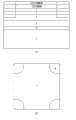
图1是本发明的未沉积金属的电极的LED芯片结构图,其中(a)为主视图,(b)为俯视图;Fig. 1 is the structure diagram of the LED chip of the electrode of the present invention without depositing metal, wherein (a) is a front view, and (b) is a top view;
图2是本发明p型电极形状,其中(a)为主视图,(b)为俯视图。Fig. 2 is the p-type electrode shape of the present invention, wherein (a) is a front view, and (b) is a top view.
具体实施方式Detailed ways
本发明的优选实例结合附图说明如下:Preferred examples of the present invention are described as follows in conjunction with accompanying drawings:
实施例一:参见图1和图2,本ITO/氧化锌基透明电极发光二极管包括:在蓝宝石衬底1上依次有缓冲层2、本征层3、n型氮化镓4、量子阱5、p型氮化镓6和透明电极7,并有n型金属电极(PAD)8连接n型氮化镓4,p型金属电极(PAD)9连接透明电极7。其中缓冲层2、本征层3、n型氮化镓4、量子阱5、p型氮化镓6是在MOCVD中依次生长完成的;所述的透明电极7是ITO/氧化锌复合透明电极,其中ITO薄膜的材质是是Sn2O3:In2O3=1:9的铟锡氧化物,氧化锌基透明导电薄膜的材质是ZnO:Ga或ZnO:Al或ZnO:In;所述的n型金属电极(8)是金属复合电极,材质是Ti/Al或Cr/Pt/Au;所属的p型金属电极(9)是金属复合电极,材质是Ni/Au或Cr/Pt/Au。Embodiment 1: Referring to Fig. 1 and Fig. 2, the present ITO/zinc oxide-based transparent electrode light-emitting diode comprises: a
实施例二:本实施例与与实施例一基本相同,特别之处是:p型电极的特殊形状:正十字架形,此种形状的p型金属电极9使得电流扩散更均匀,提高了LED芯片的可靠性。Embodiment 2: This embodiment is basically the same as Embodiment 1. The special feature is: the special shape of the p-type electrode: a positive cross shape. The p-type metal electrode 9 of this shape makes the current spread more uniform and improves the LED chip. reliability.
实施例三:本透明电极发光二极管芯片制造方法如下:首先,用MOCVD的方法在衬底上依次缓冲层2、本征层3、n型氮化镓4、量子阱5、p型氮化镓6;紧接着对外延片进行镁激活退火处理;然后使用KOH或者HCl或者王水等化学试剂对外延片进行表面处理,通过电子束蒸镀的方法沉积ITO透明导电薄膜,再通过射频磁控溅射氧化锌透明导电薄膜形成了ITO/氧化锌基复合透明电极7,用湿法腐蚀的方法,将复合透明电极腐蚀出所需图形,再通过离子刻蚀或者ICP刻蚀将n型氮化镓暴露出来,并进行退火处理;通过热蒸发或电子束蒸发的方法沉积n型金属电极(PAD)8和p型金属电极(PAD)9;最后,进行金属电极的合金化退火处理并分割外延片。Embodiment three: the manufacturing method of the transparent electrode light-emitting diode chip is as follows: first,
实施例四:本实施与实施例三基本相同,特别之处在于:所述的ITO/氧化锌基复合电极是通过直流磁控溅射沉积ITO薄膜,再通过射频磁控溅射沉积氧化锌基薄膜形成ITO/氧化锌基复合透明电极7,用湿法腐蚀的方法,将复合透明电极腐蚀出所需图形,再通过离子刻蚀将n型氮化镓暴露出来,并进行退火处理;通过热蒸发或电子束蒸发的方法沉积n型金属电极(PAD)8和p型金属电极(PAD)9;最后,进行金属电极的合金化退火处理并分割外延片。Embodiment 4: This implementation is basically the same as Embodiment 3. The special feature is that the ITO/zinc oxide-based composite electrode is deposited by DC magnetron sputtering ITO film, and then deposited by radio frequency magnetron sputtering. Form the ITO/zinc oxide-based composite
实施例五:本实施与实施例四基本相同,特别之处在于:所述的ITO/氧化锌基复合电极是通过直流磁控溅射沉积ITO薄膜,再通过射频磁控溅射沉积氧化锌基薄膜形成ITO/氧化锌基复合透明电极7后,直接通过离子刻蚀或者ICP刻蚀将n型氮化镓暴露出来,使得p型氮化镓呈现出所想要的图案。芯片尺寸为1mm×1mm,为辅助氧化锌进行更好的电流扩散,设计出此种特殊的形状的p型金属电极。氧化锌透明电极提高了LED芯片光提取效率,此种形状的p型电极使得电流扩散更均匀,从而提高了LED芯片的可靠性。Embodiment 5: This implementation is basically the same as
Claims (6)
Translated fromChinesePriority Applications (1)
| Application Number | Priority Date | Filing Date | Title |
|---|---|---|---|
| CN2011100755794ACN102169943A (en) | 2011-03-29 | 2011-03-29 | Light-emitting diode (LED) with indium tin oxide (ITO)/zinc oxide based composite transparent electrode and preparation method of LED |
Applications Claiming Priority (1)
| Application Number | Priority Date | Filing Date | Title |
|---|---|---|---|
| CN2011100755794ACN102169943A (en) | 2011-03-29 | 2011-03-29 | Light-emitting diode (LED) with indium tin oxide (ITO)/zinc oxide based composite transparent electrode and preparation method of LED |
Publications (1)
| Publication Number | Publication Date |
|---|---|
| CN102169943Atrue CN102169943A (en) | 2011-08-31 |
Family
ID=44491011
Family Applications (1)
| Application Number | Title | Priority Date | Filing Date |
|---|---|---|---|
| CN2011100755794APendingCN102169943A (en) | 2011-03-29 | 2011-03-29 | Light-emitting diode (LED) with indium tin oxide (ITO)/zinc oxide based composite transparent electrode and preparation method of LED |
Country Status (1)
| Country | Link |
|---|---|
| CN (1) | CN102169943A (en) |
Cited By (10)
| Publication number | Priority date | Publication date | Assignee | Title |
|---|---|---|---|---|
| CN102637786A (en)* | 2012-04-21 | 2012-08-15 | 浙江大学 | Method for preparing LED (light-emitting diode) electrode taking ITO/ZnO based composite film as p electrode |
| CN102916100A (en)* | 2012-11-08 | 2013-02-06 | 安徽三安光电有限公司 | Light emitting diode and manufacturing method thereof |
| CN103346231A (en)* | 2013-06-18 | 2013-10-09 | 上海大学 | Copper sulfide/oxide zinc base composite transparent electrode light-emitting diode and preparation method thereof |
| CN103346230A (en)* | 2013-06-18 | 2013-10-09 | 上海大学 | Copper sulfide/oxide zinc radical composite transparent electrode light-emitting diode and preparation method thereof |
| CN103730558A (en)* | 2013-12-31 | 2014-04-16 | 中国科学院半导体研究所 | LED adopting composite transparent conducting layer and preparation method thereof |
| CN103855255A (en)* | 2012-11-29 | 2014-06-11 | 上海蓝光科技有限公司 | Manufacturing method of light-emitting diode |
| CN105023985A (en)* | 2015-07-28 | 2015-11-04 | 聚灿光电科技股份有限公司 | LED (Light Emitting Diode) chip and preparation method thereof |
| CN109950378A (en)* | 2017-12-20 | 2019-06-28 | 大连德豪光电科技有限公司 | LED chip and preparation method thereof |
| WO2021088786A1 (en)* | 2019-11-04 | 2021-05-14 | The University Of Hong Kong | Spectral red-shifting of light-emitting diodes by indium tin oxide deposition and annealing |
| CN115312636A (en)* | 2022-10-11 | 2022-11-08 | 罗化芯显示科技开发(江苏)有限公司 | A micro light-emitting diode display panel and its manufacturing method |
Citations (1)
| Publication number | Priority date | Publication date | Assignee | Title |
|---|---|---|---|---|
| CN101789479A (en)* | 2010-01-29 | 2010-07-28 | 上海大学 | Transparent electrode LED and method for manufacturing same |
- 2011
- 2011-03-29CNCN2011100755794Apatent/CN102169943A/enactivePending
Patent Citations (1)
| Publication number | Priority date | Publication date | Assignee | Title |
|---|---|---|---|---|
| CN101789479A (en)* | 2010-01-29 | 2010-07-28 | 上海大学 | Transparent electrode LED and method for manufacturing same |
Non-Patent Citations (2)
| Title |
|---|
| 吴正杰: "《国立成功大学材料科学及工程学系硕士论文》", 30 June 2004* |
| 郝彦忠等: "ZnO纳米团簇与CdSe纳米棒复合膜的光电化学性能研究", 《功能材料》* |
Cited By (17)
| Publication number | Priority date | Publication date | Assignee | Title |
|---|---|---|---|---|
| CN102637786A (en)* | 2012-04-21 | 2012-08-15 | 浙江大学 | Method for preparing LED (light-emitting diode) electrode taking ITO/ZnO based composite film as p electrode |
| CN102637786B (en)* | 2012-04-21 | 2015-08-26 | 浙江大学 | With the LED electrical pole manufacture method that ITO ∕ zno-based composite membrane is p-electrode |
| CN102916100B (en)* | 2012-11-08 | 2015-04-08 | 安徽三安光电有限公司 | Light-emitting diode and method of making the same |
| CN102916100A (en)* | 2012-11-08 | 2013-02-06 | 安徽三安光电有限公司 | Light emitting diode and manufacturing method thereof |
| US9337384B2 (en) | 2012-11-08 | 2016-05-10 | Xiamen Sanan Optoelectronics Technology Co., Ltd. | Light-emitting diode and fabrication method thereof |
| WO2014071839A1 (en)* | 2012-11-08 | 2014-05-15 | 厦门巿三安光电科技有限公司 | Light emitting diode and manufacturing method thereof |
| CN103855255B (en)* | 2012-11-29 | 2016-08-24 | 上海蓝光科技有限公司 | A kind of manufacture method of light emitting diode |
| CN103855255A (en)* | 2012-11-29 | 2014-06-11 | 上海蓝光科技有限公司 | Manufacturing method of light-emitting diode |
| CN103346231B (en)* | 2013-06-18 | 2016-02-17 | 上海大学 | Copper sulfide/Zinc oxide-base composite transparent electrode light-emitting diode and preparation method thereof |
| CN103346230A (en)* | 2013-06-18 | 2013-10-09 | 上海大学 | Copper sulfide/oxide zinc radical composite transparent electrode light-emitting diode and preparation method thereof |
| CN103346231A (en)* | 2013-06-18 | 2013-10-09 | 上海大学 | Copper sulfide/oxide zinc base composite transparent electrode light-emitting diode and preparation method thereof |
| CN103730558A (en)* | 2013-12-31 | 2014-04-16 | 中国科学院半导体研究所 | LED adopting composite transparent conducting layer and preparation method thereof |
| CN105023985A (en)* | 2015-07-28 | 2015-11-04 | 聚灿光电科技股份有限公司 | LED (Light Emitting Diode) chip and preparation method thereof |
| CN109950378A (en)* | 2017-12-20 | 2019-06-28 | 大连德豪光电科技有限公司 | LED chip and preparation method thereof |
| WO2021088786A1 (en)* | 2019-11-04 | 2021-05-14 | The University Of Hong Kong | Spectral red-shifting of light-emitting diodes by indium tin oxide deposition and annealing |
| CN115312636A (en)* | 2022-10-11 | 2022-11-08 | 罗化芯显示科技开发(江苏)有限公司 | A micro light-emitting diode display panel and its manufacturing method |
| CN115312636B (en)* | 2022-10-11 | 2022-12-16 | 罗化芯显示科技开发(江苏)有限公司 | Micro light-emitting diode display panel and manufacturing method thereof |
Similar Documents
| Publication | Publication Date | Title |
|---|---|---|
| CN102169943A (en) | Light-emitting diode (LED) with indium tin oxide (ITO)/zinc oxide based composite transparent electrode and preparation method of LED | |
| TWI324401B (en) | Fabrication method of high-brightness light emitting diode having reflective layer | |
| CN101771119B (en) | LED (light-emitting diode) of zinc-oxide based transparent electrode and manufacturing method thereof | |
| CN1851947A (en) | Efficient full-bright all-reflection light-emitting-diode and making method | |
| CN104576872A (en) | Semiconductor LED chip and manufacturing method thereof | |
| CN102185074A (en) | Light emitting diode of Ag/zinc-oxide-based composite transparent electrode and preparation method thereof | |
| WO2015003564A1 (en) | Gallium nitride based light emitting diode and manufacturing method thereof | |
| CN102244087A (en) | Controllable power flip array light emitting diode (LED) chip and manufacturing method thereof | |
| CN1794476A (en) | Indium gallium aluminium nitrogen semi-conductor luminous element containing metallic chromium substrate and its manufacturing method | |
| CN101887938B (en) | LED chip and manufacturing method thereof | |
| CN108470809A (en) | LED chip and preparation method thereof with transparency conducting layer composite membrane group | |
| CN104617191A (en) | LED vertical chip with current block structure and preparation method thereof | |
| CN102637801A (en) | Light-emitting diode | |
| CN101789479A (en) | Transparent electrode LED and method for manufacturing same | |
| CN101777616A (en) | Zinc oxide-based transparent electrode light emitting diode and preparation method thereof | |
| CN105720142B (en) | A kind of preparation method of light-emitting diode chip for backlight unit | |
| CN102169944B (en) | Light-emitting diode of Ag/ITO/zinc oxide base composite transparent electrode and preparation method thereof | |
| CN106340574B (en) | GaAs base LED chip and preparation method with roughening current extending | |
| CN103346230A (en) | Copper sulfide/oxide zinc radical composite transparent electrode light-emitting diode and preparation method thereof | |
| CN103346231B (en) | Copper sulfide/Zinc oxide-base composite transparent electrode light-emitting diode and preparation method thereof | |
| CN104409595B (en) | Vertical light emitting diode (LED) with current blocking structures and manufacturing method thereof | |
| CN101834253A (en) | GaN-based high-power light-emitting diode with zinc oxide stacked electrode and preparation method thereof | |
| CN1779996A (en) | Laser lift-off power LED chip on metal heat sink and preparation method thereof | |
| CN108365056A (en) | A kind of light emitting diode with vertical structure and its manufacturing method | |
| CN103594591B (en) | There is the manufacture method of the inverted light-emitting diode (LED) of transparency electrode |
Legal Events
| Date | Code | Title | Description |
|---|---|---|---|
| C06 | Publication | ||
| PB01 | Publication | ||
| C10 | Entry into substantive examination | ||
| SE01 | Entry into force of request for substantive examination | ||
| C02 | Deemed withdrawal of patent application after publication (patent law 2001) | ||
| WD01 | Invention patent application deemed withdrawn after publication | Application publication date:20110831 |