CN102169829B - Integrated circuit structure and method for preventing contact hole metal from protruding into gate - Google Patents
Integrated circuit structure and method for preventing contact hole metal from protruding into gateDownload PDFInfo
- Publication number
- CN102169829B CN102169829BCN2010102881462ACN201010288146ACN102169829BCN 102169829 BCN102169829 BCN 102169829BCN 2010102881462 ACN2010102881462 ACN 2010102881462ACN 201010288146 ACN201010288146 ACN 201010288146ACN 102169829 BCN102169829 BCN 102169829B
- Authority
- CN
- China
- Prior art keywords
- contact hole
- work function
- grid
- field effect
- gate
- Prior art date
- Legal status (The legal status is an assumption and is not a legal conclusion. Google has not performed a legal analysis and makes no representation as to the accuracy of the status listed.)
- Active
Links
- 229910052751metalInorganic materials0.000titleclaimsabstractdescription147
- 239000002184metalSubstances0.000titleclaimsabstractdescription147
- 238000000034methodMethods0.000titleclaimsabstractdescription90
- 229910021420polycrystalline siliconInorganic materials0.000claimsabstractdescription114
- 229920005591polysiliconPolymers0.000claimsabstractdescription114
- 230000008569processEffects0.000claimsabstractdescription41
- 239000000758substrateSubstances0.000claimsabstractdescription38
- WFKWXMTUELFFGS-UHFFFAOYSA-NtungstenChemical compound[W]WFKWXMTUELFFGS-UHFFFAOYSA-N0.000claimsabstractdescription27
- 229910052721tungstenInorganic materials0.000claimsabstractdescription27
- 239000010937tungstenSubstances0.000claimsabstractdescription27
- 230000005669field effectEffects0.000claimsdescription66
- 238000000231atomic layer depositionMethods0.000claimsdescription23
- 238000005229chemical vapour depositionMethods0.000claimsdescription21
- 238000000151depositionMethods0.000claimsdescription21
- 239000000463materialSubstances0.000claimsdescription21
- 230000015572biosynthetic processEffects0.000claimsdescription13
- 230000008021depositionEffects0.000claimsdescription11
- 238000000059patterningMethods0.000claimsdescription9
- ATJFFYVFTNAWJD-UHFFFAOYSA-NTinChemical compound[Sn]ATJFFYVFTNAWJD-UHFFFAOYSA-N0.000claimsdescription8
- 229910052782aluminiumInorganic materials0.000claimsdescription8
- 239000007769metal materialSubstances0.000claimsdescription6
- 229910052719titaniumInorganic materials0.000claimsdescription4
- 229910052726zirconiumInorganic materials0.000claimsdescription4
- ITWBWJFEJCHKSN-UHFFFAOYSA-N1,4,7-triazonaneChemical compoundC1CNCCNCCN1ITWBWJFEJCHKSN-UHFFFAOYSA-N0.000claimsdescription3
- 229910010038TiAlInorganic materials0.000claimsdescription3
- 229910010037TiAlNInorganic materials0.000claimsdescription3
- 229910052741iridiumInorganic materials0.000claimsdescription3
- 229910052742ironInorganic materials0.000claimsdescription3
- 229910052748manganeseInorganic materials0.000claimsdescription3
- 229910052759nickelInorganic materials0.000claimsdescription3
- 229910052763palladiumInorganic materials0.000claimsdescription3
- 229910052702rheniumInorganic materials0.000claimsdescription3
- 229910052703rhodiumInorganic materials0.000claimsdescription3
- 229910052709silverInorganic materials0.000claimsdescription3
- 229910003468tantalcarbideInorganic materials0.000claimsdescription3
- 229910004166TaNInorganic materials0.000claims2
- 229910004200TaSiNInorganic materials0.000claims2
- 229910052697platinumInorganic materials0.000claims2
- 229910052707rutheniumInorganic materials0.000claims2
- 238000012545processingMethods0.000abstractdescription6
- 230000008901benefitEffects0.000abstractdescription3
- 230000004048modificationEffects0.000abstractdescription3
- 238000012986modificationMethods0.000abstractdescription3
- 238000001459lithographyMethods0.000abstractdescription2
- 239000010410layerSubstances0.000description205
- 239000011800void materialSubstances0.000description41
- 239000004065semiconductorSubstances0.000description15
- 230000004888barrier functionEffects0.000description10
- VYPSYNLAJGMNEJ-UHFFFAOYSA-NSilicium dioxideChemical compoundO=[Si]=OVYPSYNLAJGMNEJ-UHFFFAOYSA-N0.000description8
- 229920002120photoresistant polymerPolymers0.000description8
- 238000005240physical vapour depositionMethods0.000description8
- XAGFODPZIPBFFR-UHFFFAOYSA-NaluminiumChemical compound[Al]XAGFODPZIPBFFR-UHFFFAOYSA-N0.000description5
- 238000013461designMethods0.000description4
- 239000003989dielectric materialSubstances0.000description4
- 230000000694effectsEffects0.000description4
- 235000012239silicon dioxideNutrition0.000description4
- 239000000377silicon dioxideSubstances0.000description4
- 230000003068static effectEffects0.000description4
- 239000010409thin filmSubstances0.000description4
- 229910004129HfSiOInorganic materials0.000description3
- XUIMIQQOPSSXEZ-UHFFFAOYSA-NSiliconChemical compound[Si]XUIMIQQOPSSXEZ-UHFFFAOYSA-N0.000description3
- 239000012790adhesive layerSubstances0.000description3
- 238000011161developmentMethods0.000description3
- 230000018109developmental processEffects0.000description3
- 239000002019doping agentSubstances0.000description3
- 239000010408filmSubstances0.000description3
- 239000011229interlayerSubstances0.000description3
- 229910044991metal oxideInorganic materials0.000description3
- 150000004706metal oxidesChemical class0.000description3
- 229910052710siliconInorganic materials0.000description3
- 239000010703siliconSubstances0.000description3
- -1LaSiOInorganic materials0.000description2
- 229910004298SiO 2Inorganic materials0.000description2
- 230000008859changeEffects0.000description2
- 238000004519manufacturing processMethods0.000description2
- 229910052814silicon oxideInorganic materials0.000description2
- 125000006850spacer groupChemical group0.000description2
- 229910018072Al 2 O 3Inorganic materials0.000description1
- 229910017121AlSiOInorganic materials0.000description1
- 229910002367SrTiOInorganic materials0.000description1
- 238000004380ashingMethods0.000description1
- 230000000903blocking effectEffects0.000description1
- 230000000295complement effectEffects0.000description1
- 239000011521glassSubstances0.000description1
- 229910052735hafniumInorganic materials0.000description1
- 150000002500ionsChemical class0.000description1
- 238000002955isolationMethods0.000description1
- 229910052747lanthanoidInorganic materials0.000description1
- 150000002602lanthanoidsChemical class0.000description1
- 229910052746lanthanumInorganic materials0.000description1
- 238000001465metallisationMethods0.000description1
- 150000002739metalsChemical class0.000description1
- 229910052758niobiumInorganic materials0.000description1
- 229910021332silicideInorganic materials0.000description1
- FVBUAEGBCNSCDD-UHFFFAOYSA-Nsilicide(4-)Chemical compound[Si-4]FVBUAEGBCNSCDD-UHFFFAOYSA-N0.000description1
- 229910052715tantalumInorganic materials0.000description1
- 229910052720vanadiumInorganic materials0.000description1
Images


Classifications
- H—ELECTRICITY
- H10—SEMICONDUCTOR DEVICES; ELECTRIC SOLID-STATE DEVICES NOT OTHERWISE PROVIDED FOR
- H10D—INORGANIC ELECTRIC SEMICONDUCTOR DEVICES
- H10D64/00—Electrodes of devices having potential barriers
- H10D64/01—Manufacture or treatment
- H10D64/017—Manufacture or treatment using dummy gates in processes wherein at least parts of the final gates are self-aligned to the dummy gates, i.e. replacement gate processes
- H—ELECTRICITY
- H10—SEMICONDUCTOR DEVICES; ELECTRIC SOLID-STATE DEVICES NOT OTHERWISE PROVIDED FOR
- H10D—INORGANIC ELECTRIC SEMICONDUCTOR DEVICES
- H10D30/00—Field-effect transistors [FET]
- H10D30/60—Insulated-gate field-effect transistors [IGFET]
- H—ELECTRICITY
- H10—SEMICONDUCTOR DEVICES; ELECTRIC SOLID-STATE DEVICES NOT OTHERWISE PROVIDED FOR
- H10D—INORGANIC ELECTRIC SEMICONDUCTOR DEVICES
- H10D84/00—Integrated devices formed in or on semiconductor substrates that comprise only semiconducting layers, e.g. on Si wafers or on GaAs-on-Si wafers
- H10D84/01—Manufacture or treatment
- H10D84/0123—Integrating together multiple components covered by H10D12/00 or H10D30/00, e.g. integrating multiple IGBTs
- H10D84/0126—Integrating together multiple components covered by H10D12/00 or H10D30/00, e.g. integrating multiple IGBTs the components including insulated gates, e.g. IGFETs
- H10D84/0165—Integrating together multiple components covered by H10D12/00 or H10D30/00, e.g. integrating multiple IGBTs the components including insulated gates, e.g. IGFETs the components including complementary IGFETs, e.g. CMOS devices
- H10D84/0172—Manufacturing their gate conductors
- H10D84/0177—Manufacturing their gate conductors the gate conductors having different materials or different implants
- H—ELECTRICITY
- H10—SEMICONDUCTOR DEVICES; ELECTRIC SOLID-STATE DEVICES NOT OTHERWISE PROVIDED FOR
- H10D—INORGANIC ELECTRIC SEMICONDUCTOR DEVICES
- H10D84/00—Integrated devices formed in or on semiconductor substrates that comprise only semiconducting layers, e.g. on Si wafers or on GaAs-on-Si wafers
- H10D84/01—Manufacture or treatment
- H10D84/02—Manufacture or treatment characterised by using material-based technologies
- H10D84/03—Manufacture or treatment characterised by using material-based technologies using Group IV technology, e.g. silicon technology or silicon-carbide [SiC] technology
- H10D84/038—Manufacture or treatment characterised by using material-based technologies using Group IV technology, e.g. silicon technology or silicon-carbide [SiC] technology using silicon technology, e.g. SiGe
- H—ELECTRICITY
- H10—SEMICONDUCTOR DEVICES; ELECTRIC SOLID-STATE DEVICES NOT OTHERWISE PROVIDED FOR
- H10D—INORGANIC ELECTRIC SEMICONDUCTOR DEVICES
- H10D64/00—Electrodes of devices having potential barriers
- H10D64/60—Electrodes characterised by their materials
- H10D64/66—Electrodes having a conductor capacitively coupled to a semiconductor by an insulator, e.g. MIS electrodes
- H10D64/667—Electrodes having a conductor capacitively coupled to a semiconductor by an insulator, e.g. MIS electrodes the conductor comprising a layer of alloy material, compound material or organic material contacting the insulator, e.g. TiN workfunction layers
Landscapes
- Internal Circuitry In Semiconductor Integrated Circuit Devices (AREA)
- Semiconductor Memories (AREA)
Abstract
Description
Translated fromChinese技术领域technical field
本发明涉及一种金属突出物,特别涉及一种伸入取代栅极的接触孔金属。The invention relates to a metal protrusion, in particular to a contact hole metal protruding into a replacement grid.
背景技术Background technique
集成电路(IC)工业已历经快速的成长。集成电路(IC)材料和设计的技术发展已使每一个集成电路世代的电路较前一个世代小且更复杂。然而,这些发展会增加集成电路工艺和制造方法的复杂度,且为了实现这些技术发展,需要发展较简单的集成电路工艺和制造方法。The integrated circuit (IC) industry has experienced rapid growth. Technological advances in integrated circuit (IC) materials and design have resulted in each IC generation having smaller and more complex circuits than the previous generation. However, these developments increase the complexity of integrated circuit processes and manufacturing methods, and in order to realize these technological developments, simpler integrated circuit processes and manufacturing methods need to be developed.
在集成电路发展的过程中,当几何尺寸(意即可利用一工艺制造的最小元件(或线宽))缩小时,通常会增加功能密度(functional density)(意即每个芯片面积的相互连接元件的数量)。这种尺寸微缩的工艺通常具有增加工艺效率和降低成本的优点。这种尺寸微缩的工艺会使例如互补式金属氧化物半导体晶体管(以下简称CMOS)的低消耗功率元件消耗较高的功率。典型地,CMOS元件具有栅极氧化层和多晶硅栅极。在特征尺寸持续微缩的同时,为了改善元件性能,会想要以高介电常数(high-k)栅极介电层和金属栅极取代栅极氧化层和多晶硅栅极。During the development of integrated circuits, when the geometric size (meaning the smallest component (or line width) that can be manufactured by a process) shrinks, the functional density (functional density) (meaning the number of interconnections per chip area) usually increases. number of components). This size shrinking process generally has the advantages of increasing process efficiency and reducing costs. This size shrinking process will cause low power consumption devices such as complementary metal oxide semiconductor transistors (hereinafter referred to as CMOS) to consume higher power. Typically, a CMOS device has a gate oxide and a polysilicon gate. To improve device performance while feature sizes continue to shrink, it is desirable to replace gate oxide and polysilicon gates with high-k (high-k) gate dielectrics and metal gates.
然而,当要将高介电常数(high-k)栅极介电层/金属栅极与CMOS工艺整合时,会产生许多问题。因此,在此技术领域中,有需要一种防止接触孔金属伸入栅极的集成电路结构及其方法,以克服公知技术的缺点。However, many problems arise when integrating a high-k gate dielectric/metal gate with a CMOS process. Therefore, in this technical field, there is a need for an integrated circuit structure and method for preventing the contact hole metal from protruding into the gate, so as to overcome the disadvantages of the prior art.
发明内容Contents of the invention
有鉴于此,本发明实施例提供防止接触孔金属伸入栅极的集成电路结构及其方法。本发明一实施例提供一种防止一接触孔金属伸入相邻的栅极元件以影响上述些栅极元件功函数的方法。上述方法包括准备一光掩模,其用以暴露出P型场效应晶体管的栅极结构中的一虚设多晶硅,其中上述光掩模同时用以暴露出局部内连线区域的上述虚设多晶硅,上述些局部内连线区域的上述虚设多晶硅位于接触孔插塞下且相邻于连接至上述些局部内连线区域的N型场效应晶体管的栅极结构。上述方法又包括加工一基板,以定义出上述些P型场效应晶体管和上述些N型场效应晶体管的元件区域和结构,其中上述些P型场效应晶体管和上述些N型场效应晶体管的上述些栅极结构和上述些局部内连线利用一虚设多晶硅层沉积而成。上述方法又包括图案化上述基板,以暴露出位于上述些P型场效应晶体管的上述些栅极结构中和上述些局部内连线区域中的上述虚设多晶硅,且移除从上述些P型场效应晶体管的上述些栅极结构中和上述些局部内连线区域中暴露出的上述虚设多晶硅。另外,上述方法包括于上述基板上沉积具有开口的一P型功函数层,上述些开口利用移除从上述些P型场效应晶体管的上述些栅极结构中和上述些局部内连线区域中暴露出的上述虚设多晶硅形成,其中上述P型功函数层覆盖上述些开口的侧壁,且防止上述接触孔金属伸入连接至上述些内连线结构区域的上述些N型场效应晶体管的上述些栅极结构以影响其功函数。In view of this, the embodiments of the present invention provide an integrated circuit structure and a method for preventing contact hole metal from protruding into the gate. An embodiment of the present invention provides a method for preventing a contact hole metal from protruding into adjacent gate elements to affect the work function of the gate elements. The above method includes preparing a photomask, which is used to expose a dummy polysilicon in the gate structure of the P-type field effect transistor, wherein the above photomask is also used to expose the above dummy polysilicon in the local interconnection area, the above-mentioned The dummy polysilicon in the local interconnection regions is located under the contact plug and adjacent to the gate structure of the NFET connected to the local interconnection regions. The above method further includes processing a substrate to define the element regions and structures of the above P-type field effect transistors and the above-mentioned N-type field effect transistors, wherein the above-mentioned P-type field effect transistors and the above-mentioned N-type field effect transistors are The gate structures and the above local interconnections are formed by depositing a dummy polysilicon layer. The method further includes patterning the substrate to expose the dummy polysilicon located in the gate structures of the P-type field effect transistors and the local interconnection areas, and removing the dummy polysilicon from the P-type field effect transistors. The above-mentioned dummy polysilicon exposed in the above-mentioned gate structures of the effect transistor and in the above-mentioned local interconnection areas. In addition, the method includes depositing a P-type work function layer with openings on the substrate, and the openings are removed from the gate structures of the P-type field effect transistors and the local interconnection regions. The exposed dummy polysilicon is formed, wherein the above-mentioned P-type work function layer covers the sidewalls of the above-mentioned openings, and prevents the above-mentioned contact hole metal from protruding into the above-mentioned N-type field effect transistors connected to the above-mentioned interconnection structure regions. Some gate structures affect their work function.
本发明的另一实施例提供一种防止一接触孔金属伸入相邻的栅极元件以影响上述些栅极元件功函数的方法。上述方法包括准备一光掩模,其用以暴露出N型场效应晶体管的栅极结构中的一虚设多晶硅,其中上述光掩模同时用以暴露出局部内连线区域的上述虚设多晶硅,上述些局部内连线区域的上述虚设多晶硅位于接触孔插塞下方且相邻于连接至上述些局部内连线区域的P型场效应晶体管的栅极结构。上述方法又包括加工一基板,以定义出上述些P型场效应晶体管和上述些N型场效应晶体管的元件区域和结构,其中上述些P型场效应晶体管和上述些N型场效应晶体管的上述些栅极结构和上述局部内连线利用一虚设多晶硅层沉积而成。上述方法又包括图案化上述基板,以暴露出位于上述些N型场效应晶体管的上述些栅极结构中和上述些局部内连线区域中的上述虚设多晶硅,且移除从上述些N型场效应晶体管的上述些栅极结构中和上述些局部内连线区域中暴露出的上述虚设多晶硅。另外,于上述基板上沉积具有开口的一N型功函数层,上述些开口利用移除从上述些N型场效应晶体管的上述些栅极结构中和上述些局部内连线区域中暴露出的上述虚设多晶硅形成,其中上述N型功函数层覆盖上述些开口的侧壁,且防止上述接触孔金属伸入连接至上述些内连线结构区域的上述些P型场效应晶体管的上述些栅极结构以影响其功函数。Another embodiment of the present invention provides a method for preventing a contact hole metal from protruding into adjacent gate elements to affect the work function of the gate elements. The method includes preparing a photomask for exposing a dummy polysilicon in the gate structure of the NFET, wherein the photomask is also used for exposing the dummy polysilicon in the local interconnection area, the above The dummy polysilicon in the local interconnection regions is located under the contact plug and adjacent to the gate structure of the P-type field effect transistor connected to the local interconnection regions. The above method further includes processing a substrate to define the element regions and structures of the above P-type field effect transistors and the above-mentioned N-type field effect transistors, wherein the above-mentioned P-type field effect transistors and the above-mentioned N-type field effect transistors are These gate structures and the aforementioned local interconnects are deposited using a dummy polysilicon layer. The method further includes patterning the substrate to expose the dummy polysilicon located in the gate structures of the N-type field effect transistors and in the local interconnect areas, and removing the dummy polysilicon from the N-type field effect transistors. The above-mentioned dummy polysilicon exposed in the above-mentioned gate structures of the effect transistor and in the above-mentioned local interconnection areas. In addition, an N-type work function layer with openings is deposited on the above-mentioned substrate. The above-mentioned dummy polysilicon is formed, wherein the above-mentioned N-type work function layer covers the sidewalls of the above-mentioned openings, and prevents the above-mentioned contact hole metal from extending into the above-mentioned gates of the above-mentioned P-type field effect transistors connected to the above-mentioned interconnection structure regions. structure to affect its work function.
本发明的又一实施例提供一种防止一接触孔金属伸入相邻的栅极元件以影响上述些栅极元件功函数的集成电路结构。上述集成电路包括一栅极结构,其具有包括一栅极金属层的一栅极堆叠结构,其中上述栅极结构使用一虚设多晶硅且利用一取代栅极工艺形成。上述集成电路又包括以一接触孔金属材料填充的一接触孔插塞,其中上述接触孔插塞利用化学气相沉积法沉积而成,且其中上述接触孔插塞沉积于上述栅极堆叠结构的上述栅极金属层上,且上述接触孔插塞相邻于上述栅极结构,且其中位于上述接触孔插塞下方的上述栅极金属层被一功函数层环绕以防止上述接触孔金属伸入上述栅极堆叠结构。Yet another embodiment of the present invention provides an integrated circuit structure that prevents a contact hole metal from protruding into adjacent gate elements to affect the work function of the gate elements. The integrated circuit includes a gate structure having a gate stack structure including a gate metal layer, wherein the gate structure uses a dummy polysilicon and is formed using a replacement gate process. The above-mentioned integrated circuit further includes a contact hole plug filled with a contact hole metal material, wherein the above-mentioned contact hole plug is deposited by chemical vapor deposition, and wherein the above-mentioned contact hole plug is deposited on the above-mentioned gate stack structure. On the gate metal layer, and the above-mentioned contact hole plug is adjacent to the above-mentioned gate structure, and wherein the above-mentioned gate metal layer located under the above-mentioned contact hole plug is surrounded by a work function layer to prevent the above-mentioned contact hole metal from protruding into the above-mentioned Gate stack structure.
本发明的又另一实施例提供一种防止一接触孔金属伸入相邻的栅极元件以影响上述些栅极元件功函数的集成电路结构。上述集成电路包括包括一N型场效应晶体管栅极结构,其具有包括一栅极金属层的一栅极堆叠结构,其中上述N型场效应晶体管栅极结构使用一虚设多晶硅且利用一取代栅极工艺形成。上述集成电路又包括以一接触孔金属材料填充的一接触孔插塞,其中上述接触孔插塞利用化学气相沉积法沉积而成,且其中上述接触孔插塞沉积于上述栅极堆叠结构的上述栅极金属层上,且上述接触孔插塞相邻于上述N型场效应晶体管栅极结构,且其中位于上述接触孔插塞下方的上述栅极金属层被一P型功函数层环绕以防止上述接触孔金属伸入上述栅极堆叠结构,其中上述栅极金属层为一静态随机存取存储器单元的一字线。Yet another embodiment of the present invention provides an integrated circuit structure that prevents a contact hole metal from protruding into adjacent gate elements to affect the work function of the gate elements. The integrated circuit includes an NFET gate structure having a gate stack structure including a gate metal layer, wherein the NFET gate structure uses a dummy polysilicon and utilizes a replacement gate craft formation. The above-mentioned integrated circuit further includes a contact hole plug filled with a contact hole metal material, wherein the above-mentioned contact hole plug is deposited by chemical vapor deposition, and wherein the above-mentioned contact hole plug is deposited on the above-mentioned gate stack structure. On the gate metal layer, and the above-mentioned contact hole plug is adjacent to the above-mentioned N-type field effect transistor gate structure, and wherein the above-mentioned gate metal layer located under the above-mentioned contact hole plug is surrounded by a P-type work function layer to prevent The contact hole metal extends into the gate stack structure, wherein the gate metal layer is a word line of a static random access memory unit.
本发明的方法和结构可增加元件合格率和性能。The method and structure of the present invention can increase component yield and performance.
附图说明Description of drawings
图1A为本发明一实施例的部分静态随机存取存储器单元的俯视图。FIG. 1A is a top view of a portion of an SRAM cell according to an embodiment of the present invention.
图1B为沿图1A的A-A切线的剖面图。FIG. 1B is a cross-sectional view along line A-A of FIG. 1A .
图1C为沿图1A的B-B切线的剖面图。Fig. 1C is a cross-sectional view along the line B-B in Fig. 1A.
图1D为图1C的接近接触孔插塞的部分俯视图。FIG. 1D is a partial top view of the plug of FIG. 1C close to the contact hole.
图2A为图1C的俯视图,其中接触孔插塞被P型功函数层环绕。FIG. 2A is a top view of FIG. 1C , wherein the contact plug is surrounded by a P-type work function layer.
图2B为沿图2A的C-C切线的剖面图。FIG. 2B is a cross-sectional view along line C-C of FIG. 2A .
图2C为沿图2A的D-D切线的剖面图。FIG. 2C is a cross-sectional view along line D-D of FIG. 2A .
图3为本发明另一实施例的部分静态随机存取存储器单元的俯视图。FIG. 3 is a top view of some SRAM cells according to another embodiment of the present invention.
图4A为本发明一实施例的半导体元件区的剖面图。FIG. 4A is a cross-sectional view of a semiconductor device region according to an embodiment of the present invention.
图4B为本发明一实施例的用以保护N型场效应晶体管栅极结构的图案化光致抗蚀剂层。FIG. 4B is a patterned photoresist layer for protecting the gate structure of the N-type field effect transistor according to an embodiment of the present invention.
图4C为本发明一实施例的形成P型功函数层以部分填入P型场效应晶体管栅极结构的开口中。FIG. 4C shows the formation of a P-type work function layer to partially fill the opening of the gate structure of the P-type field effect transistor according to an embodiment of the present invention.
图4D为本发明一实施例的于P型场效应晶体管元件的开口中形成一空隙,且可能会或可能不会于N型场效应晶体管元件的开口中形成一空隙。FIG. 4D shows the formation of a void in the opening of the P-type field effect transistor device according to an embodiment of the present invention, and may or may not form a void in the opening of the N-type field effect transistor device.
图4E为本发明一实施例的于半导体元件区上形成接触孔插塞。FIG. 4E shows the formation of contact hole plugs on the semiconductor device region according to an embodiment of the present invention.
图5A为本发明一实施例的接触孔插塞俯视图,上述接触孔插塞位于栅极金属线上,其用做局部内连线且其相邻于栅极结构。5A is a top view of a contact plug according to an embodiment of the present invention. The contact plug is located on a gate metal line, which is used as a local interconnection line and is adjacent to the gate structure.
图5B显示移除本发明一实施例的环绕接触孔插塞的虚设多晶硅以形成开口,且利用具有良好侧壁覆盖能力的一功函数层做为上述开口的衬垫层。FIG. 5B shows removing the dummy polysilicon surrounding the contact plug to form an opening, and using a work function layer with good sidewall coverage as a liner layer for the opening according to an embodiment of the present invention.
图6为本发明一实施例的防止接触孔金属横向突出物伸入相邻金属栅极的流程图。FIG. 6 is a flow chart of preventing the metal lateral protrusion of the contact hole from protruding into the adjacent metal gate according to an embodiment of the present invention.
其中,附图标记说明如下:Wherein, the reference signs are explained as follows:
100、100’~静态随机存取存储器单元;100, 100'~static random access memory unit;
101~下拉栅极;101~pull down gate;
102~通过栅极;102~through the gate;
101’、102’~N型晶体管;101', 102'~N-type transistors;
101S、102S、501S~源极区;101S , 102S , 501S ~ source region;
101D、102D、501D~漏极区;101D , 102D , 501D ~ drain region;
103S、104S、103D、104D~接触孔插塞;103S , 104S , 103D , 104D ~ contact hole plug;
105、105’~字线;105, 105'~word line;
106、106’、506~接触孔插塞;106, 106', 506~contact hole plug;
110~栅极堆叠结构;110~gate stack structure;
120~界面层;120~interface layer;
123、124~薄膜;123, 124 ~ film;
125~侧壁;125~side wall;
126、126’~N型功函数层;126, 126'~N-type work function layer;
127~P型功函数层;127~P type work function layer;
128~长方形边界;128~rectangular boundary;
130、130’、310I、310I’、310II、310III、434~开口;130, 130', 310I , 310I ', 310II , 310III , 434~opening;
131~上边界;131~upper boundary;
132~下边界;132~lower boundary;
135~栅极金属层;135~gate metal layer;
140、140’、145R、1451、150、540、540’~空隙;140, 140', 145R , 1451 , 150, 540, 540'~gap;
141~粘着层;141~adhesive layer;
142~接触孔金属层;142~contact hole metal layer;
145~区域;145~area;
150~半导体基板;150~semiconductor substrate;
204~P阱;204~P well;
206~N阱;206~N well;
212、214~有源区;212, 214~active area;
218~虚设多晶硅层;218~dummy polysilicon layer;
230~层间介电层;230~interlayer dielectric layer;
320、320’~网点区;320, 320'~outlet area;
400~半导体元件区;400~semiconductor element area;
420n、420p、501~栅极结构;420n, 420p, 501~gate structure;
426~栅极间隙壁;426~gate spacer;
432~图案化光致抗蚀剂层;432~patterned photoresist layer;
434~沟槽;434~groove;
505~栅极金属线;505~Gate metal wire;
527~功函数层;527~work function layer;
L~长度;L ~ length;
D、W、T~宽度;D, W, T ~ width;
H~高度;H~height;
VS、M、N~区域;VS , M, N~ area;
600~工艺;600~craft;
601、602、603、605、607、608、609、610、611、612~步骤。601, 602, 603, 605, 607, 608, 609, 610, 611, 612~steps.
具体实施方式Detailed ways
以下以各实施例详细说明并伴随着附图说明的范例,做为本发明的参考依据。在附图或说明书描述中,相似或相同的部分皆使用相同的图号。且在附图中,实施例的形状或是厚度可扩大,并以简化或是方便标示。再者,附图中各元件的部分将以分别描述说明之,值得注意的是,图中未绘示或描述的元件,为本领域技术人员所知的形式,另外,特定的实施例仅为揭示本发明使用的特定方式,其并非用以限定本发明。Hereinafter, each embodiment is described in detail and examples accompanied by accompanying drawings are used as a reference basis of the present invention. In the drawings or descriptions in the specification, the same reference numerals are used for similar or identical parts. And in the drawings, the shapes or thicknesses of the embodiments may be enlarged, and marked for simplicity or convenience. Furthermore, the parts of each element in the drawings will be described separately. It should be noted that the elements not shown or described in the drawings are forms known to those skilled in the art. In addition, the specific embodiment is only A specific method used in the present invention is disclosed, which is not intended to limit the present invention.
图1A为本发明一实施例的部分静态随机存取存储器(以下简称SRAM)单元100的布局俯视图。SRAM单元100包括一下拉栅极(pulldown gate)101和一通过栅极(pass gate)102。在本实施例中,下拉栅极(pulldown gate)101和通过栅极(pass gate)102皆为N型场效应晶体管(以下简称nFET)。在下拉栅极101和通过栅极102的一侧有源极区101S和102S,且在下拉栅极101和通过栅极102的另一侧漏极区101D和102D。每一个源极区上有接触孔插塞103S和104S,且每一个漏极区上有接触孔插塞103D和104D。在布局中,接触孔插塞103S、104S、103D和104D绘制为正方形。在曝光和图案化基板之后,接触孔插塞103S、104S、103D和104D绘制为圆形。FIG. 1A is a top view of the layout of a portion of a static random access memory (SRAM)
图1A也显示一水平字线105,其可提供存取SRAM单元。在形成例如下拉栅极101和通过栅极102的栅极结构工艺期间,首先沉积一虚设多晶硅层形成字线105,在后续基板工艺中,上述虚设多晶硅层可被其他材料取代,例如铝(Al)栅极金属和N型功函数材料。下拉栅极101和通过栅极102两者皆为字线105的一部分。下拉栅极101和通过栅极102之间的部分字线105做为下拉栅极101和通过栅极102之间的局部内连线。一接触孔插塞106位于部分字线105的上方,且介于下拉栅极101和通过栅极102之间。Figure 1A also shows a
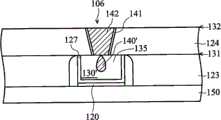
图1B为沿图1A的A-A切线的剖面图。图1A的A-A切线沿着接触孔插塞106中心位置切割。图1B显示字线105的栅极堆叠结构110和接触孔插塞106。栅极堆叠结构110包括一界面层120。界面层120可包括例如二氧化硅(SiO2)的一介电子层、一高介电常数(high-k)介电子层或一阻挡子层。界面层120可选择性包括HfSiO或SiON。上述二氧化硅介电子层沉积于基板150的表面(硅表面)上。上述高介电常数(high-k)介电子层沉积于二氧化硅介电子层的上方,且上述阻挡子层沉积于高介电常数(high-k)介电子层的上方。高介电常数(high-k)介电子层可包括例如HfOx的二元或三元高介电常数(high-k)材料薄膜。在其他实施例中,上述高介电常数(high-k)介电子层可选择性包括例如LaO、AlO、ZrO、TiO、Ta2O5、Y2O3、SrTiO3(STO)、BaTiO3(BTO)、BaZrO、HfZrO、HfLaO、HfSiO、LaSiO、AlSiO、HfTaO、HfTiO、(Ba,Sr)TiO3(BST)、Al2O3、Si3N4、氮氧化硅或其他适当材料的其他高介电常数介电材料。上述阻挡子层可包括例如TiN或TaN的金属层。在其他实施例中,阻挡子层可选择性包括Si3N4。FIG. 1B is a cross-sectional view along line AA of FIG. 1A . The tangent line AA of FIG. 1A cuts along the center of the
栅极堆叠结构110也可包括一N型功函数层126。在一实施例中,N型功函数层126的厚度可介于

在一实施例中,N型功函数层126可仅覆盖界面层120的表面。在另一实施例中,N型功函数层126也可覆盖开口130的侧壁,上述开口130被一对侧壁125包围(请看N型功函数层126’覆盖的侧壁)。剩余的开口130被例如铝的一栅极金属层135填满,且栅极金属层135具有一空隙(void)140。因为在开口130中的栅极金属层135的缺口覆盖能力(gapfill)不佳,所以会形成空隙140。栅极堆叠结构110的减少的栅极宽度D及增加的高度宽度比(aspectratio)(H/D),其中H为栅极堆叠结构110的高度,会使开口130中的栅极金属层135的缺口覆盖能力更加困难。使得空隙140变成至少一部分被用以填充接触孔插塞106的接触孔金属层填充。在一实施例中,填充接触孔插塞106的接触孔金属层可为利用化学气相沉积(CVD)法沉积的钨。然而,也可使用其他类型的金属填充接触孔插塞。In one embodiment, the N-type
在本实施例中,使用钨做为填充接触孔插塞106的金属。在沉积钨的期间,利用化学气相沉积法沉积的钨会伸入空隙140。接触孔插塞106可利用于一粘着层141做为衬垫层。在一实施例中,可利用物理气相沉积(PVD)法、化学气相沉积(CVD)法或原子层沉积(ALD)法来沉积粘着层141。在图1B中,可由一或多个介电材料形成薄膜123和124,其中薄膜123的上、下边界分别由元件符号131、132表示。In this embodiment, tungsten is used as the metal filling the
图1C为沿图1A的B-B切线的剖面图。图1A的B-B切线沿着接触孔插塞106中心位置且沿字线150切割,并垂直于A-A切线。图1C显示空隙140沿字线150的全长延伸,且显示于区域VS中。在利用化学气相沉积法沉积钨的期间,钨会伸入空隙140的位于接触孔插塞106下方的区域145,且至少一部分的钨会填充区域145。在图1C中,区域145延伸进入至少一部分的下拉栅极101和通过栅极102,且在一些实施例中,区域145可延伸进入下拉栅极101和通过栅极102的全部剖面中(区域M和N)。于空隙140中沉积钨可改变下拉栅极101和通过栅极102的nFET的功函数,且会因为通过栅极元件的高起始电压(Vt)而导致SRAM的Vcc最小值(Vcc mim)增加。Vcc最小值和起始电压(Vt)的增加会影响SRAM的性能。在一些实施例中,功函数增加的大小约为100mV至300mV之间。功函数的增加也会降低通过栅极元件的导通电流(Ion)。另外,功函数的增加也会导致元件之间的不匹配(mismatch)。因此,防止上述接触孔金属的突出甚为重要。FIG. 1C is a cross-sectional view along line BB in FIG. 1A . The tangent line BB in FIG. 1A cuts along the center of the
图1D为图1C的接近接触孔插塞106部分的俯视图(为了方便说明起见,薄膜124不做显示)。图1D显示沉积于栅极堆叠结构110侧壁上的选择性的一N型功函数层(侧壁覆盖层)126’。N型功函数层126’被称为可选择的元件是因为N型功函数晶体管126可以如图1B所示只覆盖底部。图1D显示一虚线区域145,其横向的至少一部分形成以钨沉积的空隙140。FIG. 1D is a top view of the portion of FIG. 1C near the contact plug 106 (
图2A为与图1D相同区域的俯视图,其中在接触孔插塞106的下方且环绕接触孔插塞106的栅极金属层135被P型功函数层127包围(为了方便说明起见,薄膜124不做显示)。在一实施例中,P型功函数层127为TiN层,其厚度可介于至之间。可利用原子层沉积(ALD)法、物理气相沉积(PVD)法、化学气相沉积(CVD)法或其他适合的方式形成P型功函数层127。P型功函数层127应在长方形边界128的侧壁上提供足够的覆盖能力以阻止于栅极金属层135中形成例如空隙140的细长空隙。利用化学气相沉积(CVD)法沉积钨形成的接触孔插塞106会被栅极金属层135和环绕接触孔插塞106的P型功函数层127阻挡。2A is a top view of the same area as in FIG. 1D, wherein the
原子层沉积(ALD)法具有良好的阶梯覆盖能力(step coverage)且可视为沉积P型功函数层127的适合工艺。在一实施例中,在开口侧壁上的P型功函数层127的最小值可约为在其他实施例中,P型功函数层127可选择性包括例如WN、TaN或Ru的适当形成于pFET中的其他适当材料。另外,P型功函数层127也可包括例如TiN/WN的多层结构。在一些实施例中,P型功函数材料可包括但不限于Re、Fe、Co、Rh、Ir、Ni、Pd或Pt。另外,Pd可用做为P型功函数层中的掺质。Atomic layer deposition (ALD) has good step coverage and can be regarded as a suitable process for depositing the P-type
如上所述,环绕接触孔插塞106的P型功函数层127可防止形成例如空隙140的横向细长空隙,且防止化学气相沉积(CVD)法沉积的钨突出于P型功函数层127的长方形边界128之外。图2B为沿图2A的C-C切线的剖面图。除了的N型功函数层126(和选择性的N型功函数层126’)被P型功函数层127取代之外,图2B显示与图1B非常类似的剖面图,其中P型功函数层127覆盖开口130’的侧壁和界面层120。利用例如铝的栅极金属层135填充的开口130’的剩余部分,且上述栅极金属层135具有空隙140’。因为栅极金属层135不佳的空隙覆盖能力和开口130’的高深宽比(P型功函数层127的限制),会导致空隙140’的形成。类似于图1B的空隙140,至少一部分的空隙140’被用以填充接触孔插塞106的例如钨的金属层填充。As described above, the P-type
P型功函数层127应提供良好的侧壁覆盖能力,以确保接触孔金属(例如钨)不会突出穿过未保护的侧壁到邻近nFET栅极层。在一实施例中,可利用原子层沉积(ALD)法沉积P型功函数层127,上述原子层沉积(ALD)法用以提供良好的阶梯覆盖能力。在一实施例中,可以约


图2C为沿图2A的D-D切线的剖面图。对照于图1C,空隙140’被包含于在接触孔插塞106下方的一区域中,且被栅极金属层135和P型功函数层127环绕。至少一部分的空隙140’被钨填充。即使空隙140’非常大,空隙140’和在空隙140’内部的钨仍然被栅极金属层135和P型功函数层127环绕而不会横向沿着字线105突出。边界128定义的区域的右边,可能会有因为栅极金属层135不佳的空隙覆盖能力而形成的一空隙145R。类似地,边界128定义的区域的左边,可能会有因为栅极金属层135不佳的空隙覆盖能力而形成的一空隙145L。然而,由于边界128会限制钨的突出,所以空隙145R和145L仍然会是空隙且不会被钨沉积。FIG. 2C is a cross-sectional view along line DD of FIG. 2A . In contrast to FIG. 1C , the void 140 ′ is included in a region under the
图3为本发明另一实施例的部分静态随机存取存储器(SRAM)单元100’的俯视图。SRAM单元100’非常类似于图1A的SRAM单元100,且包括额外的一字线105’。字线105’具有两个N型晶体管(nFET)101’和102’以及接触孔插塞106’。如上所述,下拉栅极101和通过栅极102也为nFET。在一实施例中,一光掩模(图未显示)的一开口310I用以暴露位于字线下方且环绕接触孔插塞106的一网点区320,且一光掩模(图未显示)的一开口310I’用以暴露位于字线下方且环绕接触孔插塞106’的一网点区320’。开口310I和310I’为长方形。如图3所示,开口310I的长度显示为L且宽度显示为W。在一实施例中,接触孔插塞106的长度L可大于接触孔插塞106的宽度W。接触孔插塞106的长度L可大于或等于字线105的宽度T。在一实施例中,接触孔插塞106的宽度W也可大于接触孔插塞106的最大尺寸(或宽度)。如图2A至图2C所示,开口310I需要够大以包围接触孔插塞106的开口下方的全部区域,以允许接触孔插塞106位于被P型功函数层127环绕的栅极金属层135上。开口310I’的设计方向遵照类似于开口310I。包括开口310I和310I’的光掩模用以移除开口中的虚设多晶硅,以允许沉积例如P型功函数层127的上述P型功函数层。FIG. 3 is a top view of a portion of a static random access memory (SRAM)
在其他的实施例中,开口310I和310I’可大于最小所需面积,且开口310I和310I’可结合形成一较大的开口,例如开口310II或开口310III。开口310II暴露位于接触孔插塞106和106’下方的虚设多晶硅。在另一实施例中,可使用开口310III。如上所述,开口310III包围接触孔插塞106的开口下方的区域,且包围多个类似于接触孔插塞106的接触孔插塞(多于接触孔插塞106和106’)。In other embodiments, openings 310I and 310I ′ may be larger than the minimum required area, and openings 310I and 310I ′ may combine to form a larger opening, such as opening 310II or opening 310III . The opening 310II exposes the dummy polysilicon under the contact plugs 106 and 106'. In another embodiment, opening 310III may be used. As mentioned above, the opening 310III surrounds the area below the opening of the
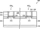
图4A为本发明一实施例的半导体元件区400的剖面图。在图4A中,半导体元件区400可包括例如硅基板的一半导体基板150。半导体基板150可更包括例如P阱204和N阱206的掺杂区。半导体元件区400可更包括用以隔绝基板的有源区212和214的隔绝结构(图未显示)。有源区212可用以构成一N型金属氧化物半导体晶体管(NMOS)(即nFET),且有源区214可用以构成一P型金属氧化物半导体晶体管(PMOS)(即pFET)。FIG. 4A is a cross-sectional view of a
半导体元件区400可包括位于nFET的有源区212元件侧中的一栅极结构420n和位于pFET的有源区214元件侧中的一栅极结构420p。栅极结构420n和420p可分别包括形成于基板150上方的一界面层120。如上所述,界面层120可包括一介电子层,例如二氧化硅(SiO2)或高介电常数(high-k)介电子层或阻挡子层。介电子层可选择性包括HfSiO或SiON。高介电常数(high-k)介电子层可包括例如HfOx的二元或三元高介电常数(high-k)材料薄膜。在其他实施例中,上述界面层120可选择性包括其他高介电常数介电材料。上述阻挡子层可包括例如TiN或TaN的金属层。在其他实施例中,上述阻挡子层可选择性包括Si3N4。上述阻挡子层可做为介于上述高介电常数(high-k)介电子层和后续工艺形成的虚设多晶硅栅极结构之间的阻挡。在后续工艺期间,上述阻挡子层可帮助降低或消除多晶硅和高介电常数(high-k)介电子层之间的费米能级钉札(Fermi level pinning)的风险。另外,在后述的移除虚设多晶硅栅极工艺期间,上述阻挡子层可做为一蚀刻停止层和保护层。应该注意的是,也可利用栅极后置工艺(gate last process)形成界面层120。半导体元件区400可更包括利用一适当工艺于界面层120上方形成的一虚设多晶硅层218。The
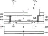
图4A可更包括不同的元件,例如轻掺杂源/漏极(LDD)区(n型或p型LDD区)、侧壁或栅极间隙壁426、源/漏极(S/D)区(n型或p型S/D区)、硅化物、接触停止层(CESL)、层间介电层(ILD)230和浅沟槽隔绝物(STI)。层间介电层(ILD)230分别填入邻近于nFET有源区212和pFET的有源区214的栅极结构420n和420p的空隙中。图4B为本发明一实施例的用以保护栅极结构420n的图案化光致抗蚀剂层432。用以形成图案化光致抗蚀剂层432图案的光掩模为具有如图3所示的开口310I(或310II、310III)的光掩模。图3所示的长度L显示于图4B中。可利用干蚀刻工艺、湿蚀刻工艺或干、湿蚀刻的组合工艺移除在pFET的有源区214的栅极结构420p中的虚设多晶硅层(栅极)218。移除虚设多晶硅层(栅极)218以于pFET的有源区214元件侧的栅极结构420p中形成一沟槽434。可利用光致抗蚀剂灰化(ashing)、光致抗蚀剂剥除(stripping)或其他适当的工艺移除图案化光致抗蚀剂层432。4A may further include different elements, such as lightly doped source/drain (LDD) regions (n-type or p-type LDD regions), sidewalls or
图4C为本发明一实施例的填入P型场效应晶体管栅极结构420p的部分沟槽434中的P型功函数层127。上述P型功函数层127为一TiN层,其厚度可介于约

分别沉积N型功函数层126(有或没有N型功函数层126’)和P型功函数层127之后,再沉积栅极金属层135。如上所述,在一实施例中,栅极金属材料例如可为铝。在图4D中,在一实施例中,在开口434中会形成一空隙140’,但在从nFET的栅极结构中移除虚设多晶硅形成的开口中可能会或可能不会形成空隙150。如果N型功函数层126覆盖开口454的侧壁(图4D的N型功函数层126’),由于上述开口的高深宽比,很可能会形成空隙150。如果N型功函数层126仅覆盖开口454的底面,较不可能形成空隙150或可能会形成较小的空隙150。图4E为本发明一实施例的形成于半导体元件区400上的接触孔插塞。图4E显示移除栅极结构420n和420p上方的栅极金属层135。沉积另一层间介电层(层)124且蚀刻层间介电层(层)124以形成接触孔开口,可利用一粘着层141和一接触孔金属层142填充上述接触孔开口。接着,移除位于例如接触孔插塞106的接触孔插塞上方的接触孔金属。在例如钨的接触孔金属沉积期间,接触孔金属会伸入在接触孔插塞106下方的例如空隙140’的空隙中。不同的是,由于空隙150并未位于或接近接触孔插塞,所以接触孔金属不会填入空隙150中。由于P型功函数层127和栅极金属层135环绕空隙140’,所以,如上所述,空隙140’中的钨不会横向伸入邻近nFET元件的栅极叠层结构(或栅极金属)中。After depositing the N-type work function layer 126 (with or without the N-type work function layer 126') and the P-type
图4A至图4E依序所示的工艺指出会先移除pFET元件的虚设多晶硅层,再移除nFET元件的虚设多晶硅层。在其他实施例中,可先移除nFET元件的虚设多晶硅层,再移除pFET元件的虚设多晶硅层。The process shown in sequence in FIGS. 4A-4E indicates that the dummy polysilicon layer of the pFET device is removed first, and then the dummy polysilicon layer of the nFET device is removed. In other embodiments, the dummy polysilicon layer of the nFET device may be removed first, and then the dummy polysilicon layer of the pFET device may be removed.
图1A和图3显示接触孔插塞106设置于SRAM的一字线150上,且接触孔插塞106设置于两个nFET元件之间。然而,如上所述实施例的接触孔插塞也可不设置于SRAM的字线上,且也可不设置于两个nFET元件之间。如上所述实施例的接触孔插塞也可设置邻近于pFET元件,以共同使用位于接触孔插塞下方的相同多晶硅区。如上所述,当nFET的虚设多晶硅移除时,也可移除位于接触孔插塞下方的虚设多晶硅。可于移除虚设多晶硅层所形成的开口中沉积一N型功函数层(取代P型功函数层),其在开口中具良好的侧壁覆盖能力。如nFET实施例所述相同的方式,N型功函数层可防止栅极金属伸入邻近pFET元件的栅极叠层结构中。1A and FIG. 3 show that the
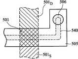
在其他实施例中,如上所述的结构和方法不仅可应用接触于具有相邻的nFET和pFET元件的SRAM的字线上。上述结构和方法也可应用位于连接至nFET和pFET元件的栅极金属的栅极金属区上的接触孔插塞。图5A为本发明一实施例的接触孔插塞506俯视图,上述接触孔插塞506位于栅极金属线505上,其用做局部内连线且其相邻于一栅极结构501。栅极结构501的元件可为具有一源极区501S和一漏极区501D的nFET元件或pFET元件。如图5A所示,栅极金属线505中会形成一空隙540,上述栅极金属线505可用做为局部内连线以将接触孔插塞506连接至栅极结构501。可使用或不使用一功函数层(图未显示)做为上述栅极金属线505的衬垫层。如图1D所示,在接触孔金属沉积期间,至少一部分空隙540可被接触孔金属填充。接触孔金属沿空隙540伸出且与栅极结构501的栅极叠层结构接触,且因此改变栅极结构501的功函数。In other embodiments, the structures and methods described above are applicable not only to contacts on word lines of SRAMs having adjacent nFET and pFET elements. The structures and methods described above are also applicable to contact plugs located on the gate metal regions connected to the gate metals of nFET and pFET elements. FIG. 5A is a top view of a
为了防止接触孔金属的突出,可移除邻近且位于接触孔插塞506下方的虚设多晶硅层,且移除虚设多晶硅层所形成的栅口可利用具有良好侧壁覆盖能力的一功函数层做为上述开口的衬垫层。图5B显示移除本发明一实施例的环绕接触孔插塞506的虚设多晶硅以形成开口,且利用具有良好侧壁覆盖能力的一功函数层527做为上述开口的衬垫层。如果栅极结构501为一nFET的栅极结构,功函数层527则为一P型功函数层。在一实施例中,由于原子层沉积(ALD)法具有良好的阶梯覆盖能力,因此可利用原子层沉积(ALD)法沉积功函数层527。图5B显示空隙540会变小成为空隙540’,且接触孔金属不会沉积于空隙中。虽然接触孔插塞506的下方会有一空隙(图未显示),但是上述空隙会被局限于利用功函数层527保护的边界内。即使接触孔插塞506下方的空隙会被接触孔金属全部填充或部分填充,被上述接触孔金属填充空隙而形成的突出物会被功函数层527限制。虽然功函数层527为导电,增加功函数层527以环绕接触孔插塞506周围的栅极金属不会影响做为内连线的栅极金属线505的本质。In order to prevent the protrusion of the contact hole metal, the dummy polysilicon layer adjacent to and under the
图6为本发明一实施例的防止接触孔金属横向突出物伸入相邻金属栅极的工艺600。在步骤601,准备用以暴露pFET元件的虚设多晶硅的一光掩模。上述光掩模也会暴露位于接触孔插塞下方且紧邻(相邻)和连接至(共用)nFET元件的相同虚设多晶硅区域的非栅极(non-gate)虚设多晶硅。在一实施例中,上述相同虚设多晶硅区域为一或多个SRAM的字线的一部分。在一实施例中,为了在设计布局中防止接触孔金属的突出物,可设计一演算法,以确认要暴露出来的上述非栅极虚设多晶硅区域。在步骤602,准备用以暴露nFET元件的虚设多晶硅的另一光掩模。在一实施例中,上述光掩模也会暴露位于接触孔插塞下方且紧邻(相邻)和连接至(共用)pFET元件的相同虚设多晶硅区域的非栅极(non-gate)虚设多晶硅。在一实施例中,上述相同虚设多晶硅区域为一或多个SRAM的字线的一部分。在一实施例中,为了在设计布局中防止接触孔金属的突出物,可设计一演算法,以确认要暴露出来的上述非栅极虚设多晶硅区域。FIG. 6 illustrates a
在步骤603,准备一基板,以定义nFET和pFET元件区和结构,上述nFET和pFET元件的栅极被虚设多晶硅填充。在步骤605,利用步骤601的光掩模,对基板进行一图案化工艺,以暴露要移除虚设多晶硅的区域。在步骤607,移除暴露出来的虚设多晶硅。步骤607可包括移除基板上的光致抗蚀剂。在步骤608,沉积一P型功函数层以覆盖基板的表面和移除虚设多晶硅所形成的开口的侧壁。在一实施例中,可利用原子层沉积(ALD)法沉积P型功函数层。如上所述,在一些实施例中,P型功函数层127的厚度可介于

在步骤608之后,在步骤609利用步骤602的光掩模进行图案化工艺,以暴露要在步骤609中移除的虚设多晶硅。如上所述,为了防止接触孔金属的突出,在步骤602准备的光掩模可包括或可不包括非栅极虚设多晶硅。在步骤610,移除在步骤609暴露出来的虚设多晶硅。在步骤611,于基板上沉积一N型功函数层以衬垫于上述开口。在一实施例中,可利用原子层沉积(ALD)法沉积N型功函数层。在步骤611之后进行步骤612以准备上述基板以形成接触孔插塞。如图4A至图4B的说明,步骤612可包括填充例如铝的栅极金属、移除nFET元件的虚设多晶硅层、利用N型功函数层和栅极金属层填充nFET元件以及形成接触孔插塞等步骤。可于西元2009年9月25日申请的美国专利申请号12/567,227的美国专利”Fabricating High-K/Metal GateDevices in a Gate Last Process”得知利用取代栅极工艺以定义元件的详细工艺,并并于本发明中以做参考。After
在一实施例中,由于位于接触孔插塞下方的栅极金属侧壁上的P型功函数层的保护,且其中上述接触孔插塞相邻于nFET元件且共用栅极金属,所以接触孔金属(例如钨)不会伸入相邻nFET元件的栅极金属区中以影响nFET元件的功函数。在另一实施例中,由于位于接触孔插塞下方的栅极金属侧壁上的P型功函数层和N型功函数层的保护,且其中上述接触孔插塞相邻于nFET和pFET元件且共用栅极金属,所以接触孔金属(例如钨)不会伸入相邻nFET和pFET元件的栅极金属区中以影响nFET和pFET元件的功函数。In one embodiment, due to the protection of the P-type work function layer on the sidewall of the gate metal under the contact hole plug, and wherein the contact hole plug is adjacent to the nFET element and shares the gate metal, the contact hole Metal, such as tungsten, does not protrude into the gate metal region of an adjacent nFET element to affect the work function of the nFET element. In another embodiment, due to the protection of the P-type work function layer and the N-type work function layer on the sidewall of the gate metal under the contact hole plug, and wherein the above-mentioned contact hole plug is adjacent to the nFET and pFET elements And the gate metal is shared, so the contact hole metal (such as tungsten) will not protrude into the gate metal region of the adjacent nFET and pFET devices to affect the work function of the nFET and pFET devices.
如上述的方法,用以暴露pFET元件的虚设多晶硅的光掩模也会暴露位于接触孔插塞下方且紧邻(相邻)和连接至(共用)nFET元件的相同虚设多晶硅区域的非栅极(non-gate)虚设多晶硅。所以用以暴露nFET元件的虚设多晶硅的光掩模不须暴露位于接触孔插塞下方且紧邻(相邻)和连接至(共用)pFET元件的相同虚设多晶硅区域的非栅极(non-gate)虚设多晶硅。在另一实施例中,用以暴露nFET元件的虚设多晶硅的光掩模也会暴露位于接触孔插塞下方且紧邻(相邻)和连接至(共用)pFET元件的相同虚设多晶硅区域的非栅极(non-gate)虚设多晶硅。所以用以暴露pFET元件的虚设多晶硅层的光掩模不须暴露位于接触孔插塞下方且紧邻(相邻)和连接至(共用)nFET元件的相同虚设多晶硅区域的非栅极(non-gate)虚设多晶硅。As in the method described above, the photomask used to expose the dummy polysilicon of the pFET element also exposes the non-gate of the same dummy polysilicon region ( non-gate) dummy polysilicon. So the photomask used to expose the dummy polysilicon of the nFET device need not expose the non-gate of the same dummy polysilicon region under the contact plug and immediately adjacent (adjacent) and connected to (shared) pFET device Dummy polysilicon. In another embodiment, the photomask used to expose the dummy polysilicon of the nFET element also exposes the non-gate of the same dummy polysilicon region located under the contact plug and immediately adjacent (adjacent) and connected to (shared) the pFET element. pole (non-gate) dummy polysilicon. Therefore, the photomask used to expose the dummy polysilicon layer of the pFET device does not have to expose the non-gate (non-gate) of the same dummy polysilicon region located under the contact plug and immediately adjacent (adjacent) and connected (shared) to the nFET device. ) dummy polysilicon.
如图6所述的工艺顺序是先图案化且移除pFET元件的虚设多晶硅层,再图案化且移除nFET元件的虚设多晶硅层。在另一实施例中,可先移除移除nFET元件的虚设多晶硅层,再移除pFET元件的虚设多晶硅层。另外,提供上述工艺600以防止钨(或接触孔金属)突出而不会影响nFET元件、pFET元件或上述两个元件组合的功函数,上述元件的功函数依用来移除虚设多晶硅层的图案化光掩模的类型而定。The process sequence as shown in FIG. 6 is to first pattern and remove the dummy polysilicon layer of the pFET device, and then pattern and remove the dummy polysilicon layer of the nFET device. In another embodiment, the dummy polysilicon layer of the nFET device may be removed first, and then the dummy polysilicon layer of the pFET device may be removed. In addition, the
上述方法和工艺防止接触孔金属(例如钨)的突出不会水平进入相邻元件的栅极叠层结构中以影响相邻元件的功函数。在一些实施例中,如果接触孔插塞和相邻元件为SRAM的一部分且位于字线上,突出的钨会使SRAM的Vcc最小值(Vcc mim)增加。邻近且位于接触孔插塞506下方的虚设多晶硅层,可利用具有良好侧壁覆盖能力的一功函数层定义位于接触孔插塞下方的金属栅极,且做为上述金属栅极的衬垫层,其中上述接触孔插塞是相邻元件且共用(或连接至)金属栅极,上述功函数层具有良好的阶梯覆盖能力以防止接触孔金属伸入相邻元件的栅极叠层结构中。本发明实施例的方法和工艺只需修改用以移除虚设多晶硅的光掩模的布局,不需额外的微影工艺及光掩模。因此,本发明实施例的方法和工艺不需修改工艺或额外的基板工艺步骤。使用上述方法和结构的好处可包括增加元件合格率和性能。The above method and process prevent the protrusion of the contact hole metal (such as tungsten) from horizontally entering the gate stack structure of the adjacent device to affect the work function of the adjacent device. In some embodiments, the protruding tungsten increases the Vcc minimum (Vcc mim ) of the SRAM if the contact plug and adjacent elements are part of the SRAM and are located on the word line. The dummy polysilicon layer adjacent to and under the
本发明一实施例提供一种防止一接触孔金属伸入相邻的栅极元件以影响该些栅极元件功函数的方法。上述方法包括准备一光掩模,其用以暴露出P型场效应晶体管的栅极结构中的一虚设多晶硅,其中该光掩模同时用以暴露出局部内连线区域的该虚设多晶硅,该些局部内连线区域的该虚设多晶硅位于接触孔插塞下且相邻于连接至该些局部内连线区域的N型场效应晶体管的栅极结构。上述方法又包括加工一基板,以定义出该些P型场效应晶体管和该些N型场效应晶体管的元件区域和结构,其中该些P型场效应晶体管和该些N型场效应晶体管的该些栅极结构和该些局部内连线利用一虚设多晶硅层沉积而成。上述方法又包括图案化该基板,以暴露出位于该些P型场效应晶体管的该些栅极结构中和该些局部内连线区域中的该虚设多晶硅,且移除从该些P型场效应晶体管的该些栅极结构中和该些局部内连线区域中暴露出的该虚设多晶硅。另外,上述方法包括于该基板上沉积具有开口的一P型功函数层,该些开口利用移除从该些P型场效应晶体管的该些栅极结构中和该些局部内连线区域中暴露出的该虚设多晶硅形成,其中该P型功函数层覆盖该些开口的侧壁,且防止该接触孔金属伸入连接至该些内连线结构区域的该些N型场效应晶体管的该些栅极结构以影响其功函数。An embodiment of the present invention provides a method for preventing a contact hole metal from protruding into adjacent gate elements to affect the work function of these gate elements. The above method includes preparing a photomask for exposing a dummy polysilicon in the gate structure of the PFET, wherein the photomask is also used for exposing the dummy polysilicon in the local interconnect area, the The dummy polysilicon of the local interconnect regions is located under the contact plugs and adjacent to gate structures of NFETs connected to the local interconnect regions. The above method further includes processing a substrate to define the element regions and structures of the P-type field effect transistors and the N-type field effect transistors, wherein the P-type field effect transistors and the N-type field effect transistors The gate structures and the local interconnects are deposited using a dummy polysilicon layer. The above method further includes patterning the substrate to expose the dummy polysilicon located in the gate structures of the P-type field effect transistors and in the local interconnection areas, and removing the dummy polysilicon from the P-type field effect transistors. The dummy polysilicon exposed in the gate structures of the effect transistors and in the local interconnection areas. In addition, the method includes depositing a P-type work function layer with openings on the substrate, and the openings are removed from the gate structures and the local interconnection regions of the P-type field effect transistors. The exposed dummy polysilicon is formed, wherein the P-type work function layer covers the sidewalls of the openings, and prevents the contact hole metal from protruding into the N-type field effect transistors connected to the interconnection structure regions. Some gate structures affect their work function.
在另一实施例中,提供一种防止一接触孔金属伸入相邻的栅极元件以影响该些栅极元件功函数的方法。上述方法包括准备一光掩模,其用以暴露出N型场效应晶体管的栅极结构中的一虚设多晶硅,其中该光掩模同时用以暴露出局部内连线区域的该虚设多晶硅,该些局部内连线区域的该虚设多晶硅位于接触孔插塞下方且相邻于连接至该些局部内连线区域的P型场效应晶体管的栅极结构。上述方法又包括加工一基板,以定义出该些P型场效应晶体管和该些N型场效应晶体管的元件区域和结构,其中该些P型场效应晶体管和该些N型场效应晶体管的该些栅极结构和该局部内连线利用一虚设多晶硅层沉积而成。上述方法又包括图案化该基板,以暴露出位于该些N型场效应晶体管的该些栅极结构中和该些局部内连线区域中的该虚设多晶硅,且移除从该些N型场效应晶体管的该些栅极结构中和该些局部内连线区域中暴露出的该虚设多晶硅。另外,于该基板上沉积具有开口的一N型功函数层,该些开口利用移除从该些N型场效应晶体管的该些栅极结构中和该些局部内连线区域中暴露出的该虚设多晶硅形成,其中该N型功函数层覆盖该些开口的侧壁,且防止该接触孔金属伸入连接至该些内连线结构区域的该些P型场效应晶体管的该些栅极结构以影响其功函数。In another embodiment, a method for preventing a contact hole metal from protruding into adjacent gate elements to affect the work function of the gate elements is provided. The above method includes preparing a photomask for exposing a dummy polysilicon in the gate structure of the NFET, wherein the photomask is also used for exposing the dummy polysilicon in the local interconnect area, the The dummy polysilicon of the local interconnect regions is located under the contact plugs and adjacent to gate structures of PFETs connected to the local interconnect regions. The above method further includes processing a substrate to define the element regions and structures of the P-type field effect transistors and the N-type field effect transistors, wherein the P-type field effect transistors and the N-type field effect transistors The gate structures and the local interconnect are deposited using a dummy polysilicon layer. The method further includes patterning the substrate to expose the dummy polysilicon located in the gate structures of the NFETs and in the local interconnect regions, and removing the dummy polysilicon from the NFETs. The dummy polysilicon exposed in the gate structures of the effect transistors and in the local interconnection areas. In addition, an N-type work function layer having openings is deposited on the substrate. The dummy polysilicon is formed, wherein the N-type work function layer covers the sidewalls of the openings and prevents the contact hole metal from protruding into the gates of the P-type field effect transistors connected to the interconnection structure regions structure to affect its work function.
在又另一实施例中,提供一种防止一接触孔金属伸入相邻的栅极元件以影响该些栅极元件功函数的集成电路结构。该集成电路包括一栅极结构,其具有包括一栅极金属层的一栅极堆叠结构,其中该栅极结构使用一虚设多晶硅且利用一取代栅极工艺形成。该集成电路又包括以一接触孔金属材料填充的一接触孔插塞,其中该接触孔插塞利用化学气相沉积法沉积而成,且其中该接触孔插塞沉积于该栅极堆叠结构的该栅极金属层上,且该接触孔插塞相邻于该栅极结构,且其中位于该接触孔插塞下方的该栅极金属层被一功函数层环绕以防止该接触孔金属伸入该栅极堆叠结构。In yet another embodiment, an integrated circuit structure is provided that prevents a contact hole metal from protruding into adjacent gate elements to affect the work function of the gate elements. The integrated circuit includes a gate structure having a gate stack structure including a gate metal layer, wherein the gate structure uses a dummy polysilicon and is formed using a replacement gate process. The integrated circuit further includes a contact hole plug filled with a contact hole metal material, wherein the contact hole plug is deposited by chemical vapor deposition, and wherein the contact hole plug is deposited on the gate stack structure. On the gate metal layer, and the contact hole plug is adjacent to the gate structure, and wherein the gate metal layer located under the contact hole plug is surrounded by a work function layer to prevent the contact hole metal from protruding into the Gate stack structure.
虽然本发明已以实施例揭示如上,然而其并非用以限定本发明,任何熟习此技艺者,在不脱离本发明的精神和范围内,当可作些许的更动与润饰,因此本发明的保护范围当视随附的权利要求所界定的范围为准。Although the present invention has been disclosed above with the embodiments, it is not intended to limit the present invention. Anyone skilled in the art can make some changes and modifications without departing from the spirit and scope of the present invention. Therefore, the present invention The scope of protection should be determined by the scope defined by the appended claims.
Claims (13)


Applications Claiming Priority (2)
| Application Number | Priority Date | Filing Date | Title |
|---|---|---|---|
| US12/713,395 | 2010-02-26 | ||
| US12/713,395US8525270B2 (en) | 2010-02-26 | 2010-02-26 | Structures and methods to stop contact metal from extruding into replacement gates |
Publications (2)
| Publication Number | Publication Date |
|---|---|
| CN102169829A CN102169829A (en) | 2011-08-31 |
| CN102169829Btrue CN102169829B (en) | 2013-10-02 |
Family
ID=44490936
Family Applications (1)
| Application Number | Title | Priority Date | Filing Date |
|---|---|---|---|
| CN2010102881462AActiveCN102169829B (en) | 2010-02-26 | 2010-09-19 | Integrated circuit structure and method for preventing contact hole metal from protruding into gate |
Country Status (2)
| Country | Link |
|---|---|
| US (2) | US8525270B2 (en) |
| CN (1) | CN102169829B (en) |
Families Citing this family (21)
| Publication number | Priority date | Publication date | Assignee | Title |
|---|---|---|---|---|
| US7888195B2 (en)* | 2008-08-26 | 2011-02-15 | United Microelectronics Corp. | Metal gate transistor and method for fabricating the same |
| US9000527B2 (en) | 2012-05-15 | 2015-04-07 | Apple Inc. | Gate stack with electrical shunt in end portion of gate stack |
| KR20140047920A (en) | 2012-10-15 | 2014-04-23 | 삼성전자주식회사 | Semiconductor device and fabricating method thereof |
| US8912584B2 (en) | 2012-10-23 | 2014-12-16 | Apple Inc. | PFET polysilicon layer with N-type end cap for electrical shunt |
| US9252259B2 (en)* | 2013-02-21 | 2016-02-02 | Taiwan Semiconductor Manufacturing Company, Ltd. | Methods and apparatus of metal gate transistors |
| US8921947B1 (en) | 2013-06-10 | 2014-12-30 | United Microelectronics Corp. | Multi-metal gate semiconductor device having triple diameter metal opening |
| US9064814B2 (en) | 2013-06-19 | 2015-06-23 | United Microelectronics Corp. | Semiconductor structure having metal gate and manufacturing method thereof |
| KR102089682B1 (en) | 2013-07-15 | 2020-03-16 | 삼성전자 주식회사 | Semiconductor device and method for fabricating the same |
| US9293333B2 (en)* | 2013-07-17 | 2016-03-22 | Globalfoundries Inc. | FinFET work function metal formation |
| US9082630B2 (en)* | 2013-11-08 | 2015-07-14 | Taiwan Semiconductor Manufacturing Co., Ltd. | Semiconductor device and fabricating method thereof |
| KR102231205B1 (en) | 2014-11-19 | 2021-03-25 | 삼성전자주식회사 | Semiconductor device and method for fabricating the same |
| US9685532B2 (en) | 2015-03-24 | 2017-06-20 | International Business Machines Corporation | Replacement metal gate structures |
| US10177240B2 (en) | 2015-09-18 | 2019-01-08 | International Business Machines Corporation | FinFET device formed by a replacement metal-gate method including a gate cut-last step |
| CN107039439B (en)* | 2016-02-04 | 2020-03-10 | 中芯国际集成电路制造(上海)有限公司 | Memory and method of forming the same |
| US10355131B2 (en) | 2016-05-17 | 2019-07-16 | Taiwan Semiconductor Manufacturing Company Ltd. | Semiconductor structure and manufacturing method thereof |
| JP6692258B2 (en)* | 2016-08-29 | 2020-05-13 | ルネサスエレクトロニクス株式会社 | Semiconductor device and manufacturing method thereof |
| CN108807158B (en)* | 2017-04-26 | 2020-10-09 | 中芯国际集成电路制造(上海)有限公司 | Semiconductor structure and forming method thereof |
| CN110634952B (en)* | 2018-06-25 | 2023-06-13 | 中芯国际集成电路制造(上海)有限公司 | Semiconductor structure and forming method thereof |
| CN115000069B (en)* | 2020-04-14 | 2025-09-16 | 福建省晋华集成电路有限公司 | Memory |
| US11282743B2 (en)* | 2020-07-17 | 2022-03-22 | Nanya Technology Corporation | Semiconductor device with multi-layer connecting structure and method for fabricating the same |
| US11640983B2 (en) | 2020-08-14 | 2023-05-02 | Taiwan Semiconductor Manufacturing Co., Ltd. | Semiconductor device and method |
Citations (1)
| Publication number | Priority date | Publication date | Assignee | Title |
|---|---|---|---|---|
| TW200826169A (en)* | 2006-10-16 | 2008-06-16 | Sony Corp | Semiconductor device and method for manufacturing same |
Family Cites Families (5)
| Publication number | Priority date | Publication date | Assignee | Title |
|---|---|---|---|---|
| TWI252539B (en)* | 2004-03-12 | 2006-04-01 | Toshiba Corp | Semiconductor device and manufacturing method therefor |
| US7229873B2 (en)* | 2005-08-10 | 2007-06-12 | Texas Instruments Incorporated | Process for manufacturing dual work function metal gates in a microelectronics device |
| KR101318946B1 (en)* | 2007-08-09 | 2013-10-17 | 삼성전자주식회사 | Test device, SRAM test device and semiconductor intergrated circuit device |
| US7838946B2 (en)* | 2008-03-28 | 2010-11-23 | United Microelectronics Corp. | Method for fabricating semiconductor structure and structure of static random access memory |
| US8222132B2 (en)* | 2008-11-14 | 2012-07-17 | Taiwan Semiconductor Manufacturing Company, Ltd. | Fabricating high-K/metal gate devices in a gate last process |
- 2010
- 2010-02-26USUS12/713,395patent/US8525270B2/enactiveActive
- 2010-09-19CNCN2010102881462Apatent/CN102169829B/enactiveActive
- 2013
- 2013-08-08USUS13/962,180patent/US9620620B2/enactiveActive
Patent Citations (1)
| Publication number | Priority date | Publication date | Assignee | Title |
|---|---|---|---|---|
| TW200826169A (en)* | 2006-10-16 | 2008-06-16 | Sony Corp | Semiconductor device and method for manufacturing same |
Also Published As
| Publication number | Publication date |
|---|---|
| US9620620B2 (en) | 2017-04-11 |
| US20130323919A1 (en) | 2013-12-05 |
| CN102169829A (en) | 2011-08-31 |
| US20110210403A1 (en) | 2011-09-01 |
| US8525270B2 (en) | 2013-09-03 |
Similar Documents
| Publication | Publication Date | Title |
|---|---|---|
| CN102169829B (en) | Integrated circuit structure and method for preventing contact hole metal from protruding into gate | |
| KR102141213B1 (en) | Negative capacitance fet with improved reliability performance | |
| US9111906B2 (en) | Method for fabricating semiconductor device having spacer elements | |
| US7947588B2 (en) | Structure and method for a CMOS device with doped conducting metal oxide as the gate electrode | |
| TWI521644B (en) | Semiconductor device and method of manufacturing same | |
| TWI408735B (en) | Semiconductor component manufacturing method | |
| US10879133B2 (en) | Replacement metal gate process for CMOS integrated circuits | |
| JP2021509536A (en) | Methods for Forming Semiconductor Structures for Vertical Transport Field Effect Transistors, Semiconductor Structures, and Integrated Circuits | |
| US20150102418A1 (en) | Semiconductor device and method for manufacturing the device | |
| US10446450B2 (en) | Static random-access memory (SRAM) devices | |
| US11508738B2 (en) | SRAM speed and margin optimization via spacer tuning | |
| US20140203375A1 (en) | Reduced Substrate Coupling for Inductors in Semiconductor Devices | |
| US10276447B2 (en) | Semiconductor structures and methods of forming the same | |
| US20240373614A1 (en) | Sram speed and margin optimization via spacer tuning | |
| CN112436004A (en) | Semiconductor element and manufacturing method thereof | |
| US11315835B2 (en) | Methods of forming an IC product comprising transistor devices with different threshold voltage levels | |
| US20210391339A1 (en) | Static random access memory and method for fabricating the same | |
| JP2010062499A (en) | Semiconductor device and method of manufacturing semiconductor device | |
| US12020950B2 (en) | Semiconductor structure and method for forming thereof | |
| CN115915770A (en) | Semiconductor device and manufacturing method thereof | |
| TWI898765B (en) | Static random access memory and method for fabricating the same | |
| US20240224518A1 (en) | Semiconductor device and method of fabricating the same | |
| US20250311359A1 (en) | Semiconductor structure with dielectric gate cap | |
| US20240088263A1 (en) | Manufacturing method of integrated circuit device | |
| US20240395817A1 (en) | Tuning Work Functions of Complementary Transistors |
Legal Events
| Date | Code | Title | Description |
|---|---|---|---|
| C06 | Publication | ||
| PB01 | Publication | ||
| C10 | Entry into substantive examination | ||
| SE01 | Entry into force of request for substantive examination | ||
| C14 | Grant of patent or utility model | ||
| GR01 | Patent grant | ||
| TR01 | Transfer of patent right | ||
| TR01 | Transfer of patent right | Effective date of registration:20250207 Address after:texas Patentee after:Palabelen Strategic Opportunities Fund LLC Country or region after:U.S.A. Address before:Hsinchu City, Taiwan, China Patentee before:Taiwan Semiconductor Manufacturing Co.,Ltd. Country or region before:TaiWan, China |