CN102163109B - Touch sensing system, capacitance sensing device and capacitance sensing method - Google Patents
Touch sensing system, capacitance sensing device and capacitance sensing methodDownload PDFInfo
- Publication number
- CN102163109B CN102163109BCN 201010121353CN201010121353ACN102163109BCN 102163109 BCN102163109 BCN 102163109BCN 201010121353CN201010121353CN 201010121353CN 201010121353 ACN201010121353 ACN 201010121353ACN 102163109 BCN102163109 BCN 102163109B
- Authority
- CN
- China
- Prior art keywords
- charge
- measured
- difference
- capacitance value
- capacitance
- Prior art date
- Legal status (The legal status is an assumption and is not a legal conclusion. Google has not performed a legal analysis and makes no representation as to the accuracy of the status listed.)
- Expired - Fee Related
Links
- 238000000034methodMethods0.000titleclaimsabstractdescription23
- 239000003990capacitorSubstances0.000claimsabstractdescription149
- 238000006243chemical reactionMethods0.000claimsdescription115
- 238000005259measurementMethods0.000abstractdescription24
- 238000010586diagramMethods0.000description38
- 230000008859changeEffects0.000description11
- 238000003860storageMethods0.000description8
- 238000009826distributionMethods0.000description5
- 241000699666Mus <mouse, genus>Species0.000description2
- 238000012986modificationMethods0.000description2
- 230000004048modificationEffects0.000description2
- 241000282414Homo sapiensSpecies0.000description1
- 241000699670Mus sp.Species0.000description1
- 230000009471actionEffects0.000description1
- 230000003247decreasing effectEffects0.000description1
- 230000001419dependent effectEffects0.000description1
- 238000001514detection methodMethods0.000description1
- 238000007599dischargingMethods0.000description1
- 238000004519manufacturing processMethods0.000description1
- 239000000758substrateSubstances0.000description1
Images


Landscapes
- Measurement Of Resistance Or Impedance (AREA)
Abstract
Description
Translated fromChinese技术领域technical field
本发明涉及一种感测装置及其方法,尤其涉及一种触控感测系统、电容感测装置及电容感测方法。The present invention relates to a sensing device and method thereof, in particular to a touch sensing system, a capacitive sensing device and a capacitive sensing method.
背景技术Background technique
在现今信息时代中,人类对于电子产品的依赖性与日俱增。笔记型电脑、移动电话、个人数字助理器(personal digital assistant,简称为:PDA)、数字随身听等电子产品均已成为现代人生活及工作中不可或缺的应用工具。上述的电子产品均具有一输入界面,用以输入使用者所须指令,以使电子产品的内部系统自动执行此项指令。目前使用最广泛的输入界面装置包括键盘(keyboard)以及鼠标(mouse)。In today's information age, human beings are increasingly dependent on electronic products. Notebook computers, mobile phones, personal digital assistants (PDA for short), digital walkmans and other electronic products have become indispensable application tools in the life and work of modern people. The above-mentioned electronic products all have an input interface for inputting the user's desired command, so that the internal system of the electronic product automatically executes the command. Currently, the most widely used input interface devices include a keyboard and a mouse.
对于使用者来说,使用键盘、鼠标等传统的输入界面在部分的场合无疑会造成相当大的不便。为了解决这样的问题,制造商便开始电子装置上配置一个例如是触控板(touch pad)或触控面板(touch panel)等的触控输入界面,进而通过触控板或触控面板来取代键盘或鼠标的功能。就触控输入界面而言,目前使用者大都是利用手指或触控笔与触控输入界面之间所产生的接触或感应行为来进行点选动作。以电容式触控输入界面而言,可多点触控的特性提供更人性化的操作模式而使得电容式触控面板逐渐受到市场的青睐。For users, using traditional input interfaces such as keyboards and mice will undoubtedly cause considerable inconvenience in some occasions. In order to solve such problems, manufacturers have begun to configure a touch input interface such as a touch pad or a touch panel on the electronic device, and then replace it with a touch pad or a touch panel. Function of the keyboard or mouse. As far as the touch input interface is concerned, currently users mostly use the contact or sensing behavior generated between the finger or stylus and the touch input interface to perform a click action. As far as the capacitive touch input interface is concerned, the multi-touch feature provides a more user-friendly operation mode, so that the capacitive touch panel is gradually favored by the market.
不过,在电容式触控输入界面中,若是使用单端式的感测电路,在测量待测电容的感应变化前,都必须先测量并储存待测电容的电容值,以作为基底(base line)。之后,再把实际测量到的待测电容值减去基底,以取得待测电容的感应变化。同时,单端式的感测电路,其待测电容的测量参考值为固定,因此感测电路必须预留较大的电压空间,以涵盖较大的感应变化,但其准确度就相对不足。However, in the capacitive touch input interface, if a single-ended sensing circuit is used, the capacitance value of the capacitor under test must be measured and stored as a base line before measuring the sensing change of the capacitor under test. ). Afterwards, the substrate is subtracted from the actual measured capacitance value to obtain the induced change of the capacitance to be measured. At the same time, the single-ended sensing circuit has a fixed measurement reference value of the capacitance to be measured, so the sensing circuit must reserve a large voltage space to cover large sensing changes, but its accuracy is relatively insufficient.
发明内容Contents of the invention
本发明的目的是提供一种电容感测装置,其可调整待测电容的测量参考值,使其测量结果较为准确,进而提升其测量效率。The purpose of the present invention is to provide a capacitance sensing device, which can adjust the measurement reference value of the capacitance to be measured to make the measurement result more accurate, thereby improving the measurement efficiency.
本发明的目的是提供一种触控感测系统,其利用电容感测装置调整待测电容的测量参考值,使其测量结果较为准确,进而提升其测量效率。The purpose of the present invention is to provide a touch sensing system, which uses a capacitive sensing device to adjust the measurement reference value of the capacitance to be measured to make the measurement result more accurate, thereby improving the measurement efficiency.
本发明的目的是提供一种电容感测方法,其可调整待测电容的测量参考值,使其测量结果较准确,进而提升其测量效率。The object of the present invention is to provide a capacitance sensing method, which can adjust the measurement reference value of the capacitance to be measured to make the measurement result more accurate, thereby improving the measurement efficiency.
本发明一实施例提供一种电容感测装置,其包括多个开关单元及一差分感测电路。每一开关单元具有一第一端、一第二端及一第三端,且每一开关单元的第三端连接至对应的感测电容。差分感测电路具有一待测输入端、一参考输入端及一输出端。差分感测电路的待测输入端连接至每一开关单元的第一端,并接收感测电容的至少其中一个所提供的一待测电容值,且差分感测电路的参考输入端连接至每一开关单元的第二端,并接收感测电容的至少其中一个所提供的一参考电容值。在此,差分感测电路比较待测电容值与参考电容值,以在输出端输出对应于待测电容值与参考电容值的一第一差值。An embodiment of the invention provides a capacitive sensing device, which includes a plurality of switch units and a differential sensing circuit. Each switch unit has a first terminal, a second terminal and a third terminal, and the third terminal of each switch unit is connected to the corresponding sensing capacitor. The differential sensing circuit has a test input terminal, a reference input terminal and an output terminal. The input terminal to be tested of the differential sensing circuit is connected to the first terminal of each switch unit, and receives a capacitance value to be measured provided by at least one of the sensing capacitors, and the reference input terminal of the differential sensing circuit is connected to each The second terminal of a switch unit receives a reference capacitance value provided by at least one of the sensing capacitances. Here, the differential sensing circuit compares the measured capacitance value with the reference capacitance value, so as to output a first difference corresponding to the measured capacitance value and the reference capacitance value at the output terminal.
本发明一实施例提供一种触控感测系统,其包括一触控输入界面及至少一电容感测装置。触控输入界面包括多个感测电容,且电容感测装置包括多个开关单元及一差分感测电路。每一开关单元具有一第一端、一第二端及一第三端,且每一开关单元的第三端连接至对应的感测电容。差分感测电路具有一待测输入端、一参考输入端及一输出端。差分感测电路的待测输入端连接至每一开关单元的第一端,并接收感测电容的至少其中一个所提供的一待测电容值,且差分感测电路的参考输入端连接至每一开关单元的第二端,并接收感测电容的至少其中一个所提供的一参考电容值。在此,差分感测电路比较待测电容值与参考电容值,以在输出端输出对应于待测电容值与参考电容值的一第一差值。An embodiment of the present invention provides a touch sensing system, which includes a touch input interface and at least one capacitive sensing device. The touch input interface includes a plurality of sensing capacitors, and the capacitive sensing device includes a plurality of switch units and a differential sensing circuit. Each switch unit has a first terminal, a second terminal and a third terminal, and the third terminal of each switch unit is connected to the corresponding sensing capacitor. The differential sensing circuit has a test input terminal, a reference input terminal and an output terminal. The input terminal to be tested of the differential sensing circuit is connected to the first terminal of each switch unit, and receives a capacitance value to be measured provided by at least one of the sensing capacitors, and the reference input terminal of the differential sensing circuit is connected to each The second terminal of a switch unit receives a reference capacitance value provided by at least one of the sensing capacitances. Here, the differential sensing circuit compares the measured capacitance value with the reference capacitance value, so as to output a first difference corresponding to the measured capacitance value and the reference capacitance value at the output terminal.
在本发明的一实施例中,上述的每一开关单元包括一第一开关及一第二开关。第一开关具有一第一端及一第二端。第一开关的第一端连接至对应的感测电容,且第一开关的第二端连接至差分感测电路的待测输入端。第二开关具有一第一端及一第二端。第二开关的第一端连接至第一开关的第一端,且第二开关的第二端连接至差分感测电路的参考输入端。In an embodiment of the present invention, each of the aforementioned switch units includes a first switch and a second switch. The first switch has a first end and a second end. The first terminal of the first switch is connected to the corresponding sensing capacitor, and the second terminal of the first switch is connected to the input terminal to be tested of the differential sensing circuit. The second switch has a first end and a second end. The first terminal of the second switch is connected to the first terminal of the first switch, and the second terminal of the second switch is connected to the reference input terminal of the differential sensing circuit.
在本发明的一实施例中,上述的差分感测电路包括一第一电荷电压转换电路、一第二电荷电压转换电路及一差值比较单元。第一电荷电压转换电路连接至每一开关单元的第一端,用以接收待测电容值,且第一电荷电压转换电路将待测电容值转换为一待测电压值。第二电荷电压转换电路连接至每一开关单元的第二端,用以接收参考电容值,且第二电荷电压转换电路将参考电容值转换为一参考电压值。差值比较单元具有一第一输入端、一第二输入端及一输出端。差值比较单元的第一输入端连接至第一电荷电压转换电路,用以接收待测电压值,且第二输入端连接至第二电荷电压转换电路,用以接收参考电压值。在此,差值比较单元比较待测电压值与参考电压值,以在输出端输出第一差值。In an embodiment of the present invention, the above-mentioned differential sensing circuit includes a first charge-to-voltage conversion circuit, a second charge-to-voltage conversion circuit and a difference comparison unit. The first charge-to-voltage conversion circuit is connected to the first end of each switch unit for receiving the capacitance value to be measured, and the first charge-to-voltage conversion circuit converts the capacitance value to be measured into a voltage value to be measured. The second charge-to-voltage conversion circuit is connected to the second terminal of each switch unit for receiving the reference capacitance value, and the second charge-to-voltage conversion circuit converts the reference capacitance value into a reference voltage value. The difference comparison unit has a first input terminal, a second input terminal and an output terminal. The first input end of the difference comparison unit is connected to the first charge-voltage conversion circuit for receiving the voltage to be measured, and the second input end is connected to the second charge-voltage conversion circuit for receiving the reference voltage value. Here, the difference comparison unit compares the voltage to be measured with the reference voltage to output a first difference at the output terminal.
在本发明的一实施例中,上述的差分感测电路包括一电荷极性转换电路、一电荷电压转换电路及一差值比较单元。电荷极性转换电路连接至每一开关单元的第二端,用以接收参考电容值所对应的一参考电荷,并转换参考电荷的极性。电荷电压转换电路连接至每一开关单元的第一端,用以接收待测电容值所对应的一待测电荷及极性转换后的参考电荷。在此,待测电荷的极性与参考电荷的极性不同,且待测电荷与参考电荷形成一第二差值。电荷电压转换电路转换第二差值为第一差值。差值比较单元连接至电荷电压转换电路,用以接收、放大并输出第一差值。In an embodiment of the present invention, the above-mentioned differential sensing circuit includes a charge polarity conversion circuit, a charge voltage conversion circuit and a difference comparison unit. The charge polarity conversion circuit is connected to the second terminal of each switch unit for receiving a reference charge corresponding to the reference capacitance value and converting the polarity of the reference charge. The charge-to-voltage conversion circuit is connected to the first end of each switch unit for receiving a test charge corresponding to the capacitance value to be measured and a reference charge after polarity conversion. Here, the polarity of the charge to be measured is different from that of the reference charge, and a second difference is formed between the charge to be measured and the reference charge. The charge-to-voltage conversion circuit converts the second difference into the first difference. The difference comparison unit is connected to the charge-to-voltage conversion circuit for receiving, amplifying and outputting the first difference.
在本发明的一实施例中,上述的差分感测电路包括一电荷极性转换电路以及一差值比较单元。电荷极性转换电路连接至每一开关单元的第一端,用以接收待测电容值所对应的一待测电荷,并转换待测电荷的极性。差值比较单元,连接至每一开关单元的第二端,用以接收参考电容值所对应的一参考电荷及极性转换后的待测电荷。在此,待测电荷的极性与参考电荷的极性不同。待测电荷与参考电荷形成一第二差值,且差值比较单元转换第二差值为第一差值,并输出第一差值。In an embodiment of the present invention, the above-mentioned differential sensing circuit includes a charge polarity conversion circuit and a difference comparison unit. The charge polarity conversion circuit is connected to the first terminal of each switch unit, and is used for receiving a charge to be measured corresponding to the capacitance to be measured, and converting the polarity of the charge to be measured. The difference comparison unit is connected to the second terminal of each switch unit, and is used for receiving a reference charge corresponding to the reference capacitance value and the charge to be measured after polarity conversion. Here, the polarity of the charge to be measured is different from that of the reference charge. The charge to be measured and the reference charge form a second difference, and the difference comparison unit converts the second difference into a first difference, and outputs the first difference.
在本发明的一实施例中,上述的差分感测电路还包括一电荷非极性转换电路,其连接于差值比较单元与每一开关单元的第二端之间。In an embodiment of the present invention, the above-mentioned differential sensing circuit further includes a charge non-polarity conversion circuit connected between the difference comparison unit and the second terminal of each switch unit.
在本发明的一实施例中,上述的差分感测电路包括一电荷极性转换电路以及一差值比较单元。电荷极性转换电路连接至每一开关单元的第二端,用以接收参考电容值所对应的一参考电荷,并转换参考电荷的极性。差值比较单元连接至每一开关单元的第一端,用以接收待测电容值所对应的一待测电荷及极性转换后的参考电荷。在此,待测电荷的极性与参考电荷的极性不同。待测电荷与参考电荷形成一第二差值,且差值比较单元转换第二差值为第一差值,并输出第一差值。In an embodiment of the present invention, the above-mentioned differential sensing circuit includes a charge polarity conversion circuit and a difference comparison unit. The charge polarity conversion circuit is connected to the second terminal of each switch unit for receiving a reference charge corresponding to the reference capacitance value and converting the polarity of the reference charge. The difference comparison unit is connected to the first end of each switch unit for receiving a charge to be measured corresponding to the capacitance to be measured and a reference charge after polarity conversion. Here, the polarity of the charge to be measured is different from that of the reference charge. The charge to be measured and the reference charge form a second difference, and the difference comparison unit converts the second difference into a first difference, and outputs the first difference.
在本发明的一实施例中,上述的差分感测电路还包括一电荷非极性转换电路,其连接于差值比较单元与每一开关单元的第一端之间。In an embodiment of the present invention, the above-mentioned differential sensing circuit further includes a charge non-polarity conversion circuit connected between the difference comparison unit and the first end of each switch unit.
在本发明的一实施例中,上述的差分感测电路包括一差分放大器、一比较器或一积分器。In an embodiment of the present invention, the above-mentioned differential sensing circuit includes a differential amplifier, a comparator or an integrator.
本发明的另一实施例提供一种电容感测方法,其包括如下步骤。提供多个开关单元及一差分感测电路,其中每一开关单元连接至对应的感测电容。接收感测电容的至少其中一个所提供的一待测电容值,并接收感测电容的至少其中一个所提供的一参考电容值。比较待测电容值与参考电容值,以产生对应于待测电容值与参考电容值的一第一差值。Another embodiment of the present invention provides a capacitance sensing method, which includes the following steps. A plurality of switch units and a differential sensing circuit are provided, wherein each switch unit is connected to a corresponding sensing capacitor. A capacitance value to be measured provided by at least one of the sensing capacitors is received, and a reference capacitance value provided by at least one of the sensing capacitors is received. The capacitance to be tested is compared with the reference capacitance to generate a first difference corresponding to the capacitance to be tested and the reference capacitance.
在本发明的一实施例中,上述的电容感测方法还包括如下步骤。在接收待测电容值后,转换待测电容值为一待测电压值。在接收参考电容值后,转换参考电容值为一参考电压值。In an embodiment of the present invention, the above capacitance sensing method further includes the following steps. After receiving the capacitance value to be measured, the capacitance value to be measured is converted to a voltage value to be measured. After receiving the reference capacitor value, converting the reference capacitor value to a reference voltage value.
在本发明的一实施例中,在比较待测电容值与参考电容值的步骤中,比较待测电压值与参考电压值,以产生第一差值。In an embodiment of the present invention, in the step of comparing the measured capacitance value and the reference capacitance value, the measured voltage value is compared with the reference voltage value to generate a first difference.
在本发明的一实施例中,在接收参考电容值的步骤中,接收参考电容值的所对应的一参考电荷,并转换参考电荷的极性。在接收待测电容值的步骤中,接收待测电容值的所对应的一待测电荷,其中待测电荷的极性与参考电荷的极性不同。In an embodiment of the present invention, in the step of receiving the reference capacitance value, a reference charge corresponding to the reference capacitance value is received, and the polarity of the reference charge is switched. In the step of receiving the capacitance value to be measured, a charge to be measured corresponding to the capacitance value to be measured is received, wherein the polarity of the charge to be measured is different from that of the reference charge.
在本发明的一实施例中,上述的电容感测方法还包括接收待测电荷及极性转换后的参考电荷,以产生一第二差值。In an embodiment of the present invention, the above capacitance sensing method further includes receiving the charge to be measured and the reference charge after polarity conversion to generate a second difference.
在本发明的一实施例中,在比较待测电容值与参考电容值的步骤中,转换第二差值为第一差值,以产生对应于待测电容值与参考电容值的第一差值。In an embodiment of the present invention, in the step of comparing the capacitance value to be measured with the reference capacitance value, the second difference is converted to the first difference value, so as to generate the first difference corresponding to the capacitance value to be measured and the reference capacitance value value.
在本发明的一实施例中,在接收参考电容值的步骤中,接收参考电容值的所对应的一参考电荷。在接收待测电容值的步骤中,接收待测电容值的所对应的一待测电荷,并转换待测电荷的极性,其中待测电荷的极性与参考电荷的极性不同。In an embodiment of the present invention, in the step of receiving the reference capacitance value, a reference charge corresponding to the reference capacitance value is received. In the step of receiving the capacitance value to be measured, a charge to be measured corresponding to the capacitance value to be measured is received, and the polarity of the charge to be measured is converted, wherein the polarity of the charge to be measured is different from that of the reference charge.
在本发明的一实施例中,上述的电容感测方法还包括接收参考电荷及极性转换后的待测电荷,以产生一第二差值。In an embodiment of the present invention, the above capacitance sensing method further includes receiving a reference charge and a polarity-converted charge to be measured to generate a second difference.
在本发明的一实施例中,在比较待测电容值与参考电容值的步骤中,转换第二差值为第一差值,以产生对应于待测电容值与参考电容值的第一差值。In an embodiment of the present invention, in the step of comparing the capacitance value to be measured with the reference capacitance value, the second difference is converted to the first difference value, so as to generate the first difference corresponding to the capacitance value to be measured and the reference capacitance value value.
在本发明的一实施例中,在比较待测电容值与参考电容值的步骤中,通过一差分放大器、一比较器或一积分器产生第一差值。In an embodiment of the present invention, in the step of comparing the capacitance to be measured with the reference capacitance, a differential amplifier, a comparator or an integrator is used to generate a first difference.
基于上述,在本发明的实施例中,电容感测装置可控制开关单元,使差分感测电路的参考输入端接收感测电容的至少其中一个所提供的参考电容值,以作为待测电容测量时的参考电容值。因此,电容感测装置可调整待测电容的测量参考值,使其测量结果较为准确,进而提升其测量效率。Based on the above, in an embodiment of the present invention, the capacitance sensing device can control the switch unit so that the reference input terminal of the differential sensing circuit receives the reference capacitance value provided by at least one of the sensing capacitances as the capacitance to be measured. when the reference capacitance value. Therefore, the capacitance sensing device can adjust the measurement reference value of the capacitance to be measured to make the measurement result more accurate, thereby improving the measurement efficiency.
为让本发明的上述特征和优点能更明显易懂,下文特举实施例,并结合附图作详细说明如下。In order to make the above-mentioned features and advantages of the present invention more comprehensible, the following specific embodiments are described in detail with reference to the accompanying drawings.
附图说明Description of drawings
图1为本发明一实施例的触控感测系统的电路方块图。FIG. 1 is a circuit block diagram of a touch sensing system according to an embodiment of the present invention.
图2A为图1的电容感测装置的电路方块图。FIG. 2A is a circuit block diagram of the capacitive sensing device of FIG. 1 .
图2B为图2A的开关单元的电路示意图。FIG. 2B is a schematic circuit diagram of the switch unit in FIG. 2A .
图3为图2A的电容感测装置的电路示意图。FIG. 3 is a schematic circuit diagram of the capacitive sensing device shown in FIG. 2A .
图4为图2A的电容感测装置的电路示意图。FIG. 4 is a schematic circuit diagram of the capacitive sensing device shown in FIG. 2A .
图5为图2A的电容感测装置的感测电容的电容值分布图。FIG. 5 is a distribution diagram of capacitance values of sensing capacitors of the capacitance sensing device of FIG. 2A .
图6为图3的电容感测装置的电路示意图。FIG. 6 is a schematic circuit diagram of the capacitive sensing device of FIG. 3 .
图7为电容感测装置动作时的时脉波形图。FIG. 7 is a clock waveform diagram when the capacitive sensing device operates.
图8为图3的电容感测装置的另一电路示意图。FIG. 8 is another schematic circuit diagram of the capacitive sensing device of FIG. 3 .
图9为本发明一实施例的电容感测装置的电路方块图。FIG. 9 is a circuit block diagram of a capacitive sensing device according to an embodiment of the present invention.
图10A为本发明第一实施例的电容感测装置的电路示意图。FIG. 10A is a schematic circuit diagram of the capacitive sensing device according to the first embodiment of the present invention.
图10B为本发明第二实施例的电容感测装置的电路示意图。FIG. 10B is a schematic circuit diagram of a capacitive sensing device according to a second embodiment of the present invention.
图10C为又一电容感测装置动作时的时脉波形图。FIG. 10C is a clock waveform diagram of another capacitive sensing device in operation.
图11为本发明第三实施例的电容感测装置的电路示意图。FIG. 11 is a schematic circuit diagram of a capacitive sensing device according to a third embodiment of the present invention.
图12A为本发明第四实施例的电容感测装置的电路示意图。FIG. 12A is a schematic circuit diagram of a capacitive sensing device according to a fourth embodiment of the present invention.
图12B为本发明第五实施例的电容感测装置的电路示意图。12B is a schematic circuit diagram of a capacitive sensing device according to a fifth embodiment of the present invention.
图13为本发明一实施例的电容感测方法的步骤流程图。FIG. 13 is a flow chart of steps of a capacitance sensing method according to an embodiment of the present invention.
主要元件符号说明:Description of main component symbols:
100:触控感测系统; 120:触控输入界面;100: touch sensing system; 120: touch input interface;
220:第二开关; 210:第一开关;220: second switch; 210: first switch;
112a~112f、114a~114f:开关; A、B、D、E、F、G:节点;112a~112f, 114a~114f: switches; A, B, D, E, F, G: nodes;
Φ0、Φ1、Φ2:时脉信号; C(1)~C(i):感测电容;Φ0 , Φ1 , Φ2 : clock signal; C(1)~C(i): sensing capacitance;
ΔC:电容变化; SW1~SWi:开关单元;ΔC: Capacitance change; SW1 ~SWi : Switch unit;
C1~C4:储存电容; Vcc:系统电压;C1~C4: storage capacitor; Vcc: system voltage;
C5~C12:电容;C5~C12: capacitance;
S1(1)~S1(i)、S2(1)~S2(i):控制信号;S1 (1)~S1 (i), S2 (1)~S2 (i): control signal;
1114、1114”:电荷非极性转换电路;1114, 1114": charge non-polar conversion circuit;
S1100、S1102、S1104、S1106:步骤;S1100, S1102, S1104, S1106: steps;
116、916、1016、1116:差值比较单元;116, 916, 1016, 1116: difference comparison unit;
112、114、112’、114’、912、1012、1012’:电荷电压转换电路;112, 114, 112', 114', 912, 1012, 1012': charge-voltage conversion circuit;
118、118’、918、1018、1018’、1118、1118’、1118”:差分感测电路;118, 118', 918, 1018, 1018', 1118, 1118', 1118": differential sensing circuit;
110、910、1010、1110、1010’、1110’、1110”:电容感测装置;110, 910, 1010, 1110, 1010', 1110', 1110": capacitive sensing means;
914、1014、1014’、1112:电荷极性转换电路。914, 1014, 1014', 1112: charge polarity conversion circuit.
具体实施方式Detailed ways
在电容式触控输入界面中,感测电容的电容值是依据感测电容对应于触控输入界面上的位置是否被触碰而决定。当感测电容对应于触控输入界面上的位置被触碰时,触碰物体会产生一对应的电容变化,而与感测电容形成一待测电容。In the capacitive touch input interface, the capacitance value of the sensing capacitor is determined according to whether the position corresponding to the sensing capacitor on the touch input interface is touched. When the sensing capacitor is touched corresponding to the position on the touch input interface, the touched object will generate a corresponding capacitance change, and form a capacitance to be measured with the sensing capacitor.
在本发明的实施例中,除了待测电容以外,其他的感测电容的电容值可作为测量待测电容时的参考值。因此,在比较待测电容值与参考电容值后,便可决定触碰物体对应于触控输入界面的触碰位置。In the embodiment of the present invention, besides the capacitance to be measured, capacitance values of other sensing capacitors can be used as reference values when measuring the capacitance to be measured. Therefore, after comparing the capacitance value to be measured with the reference capacitance value, the touch position of the touch object corresponding to the touch input interface can be determined.
在底下的实施例中,将以触控面板做为触控输入界面的范例实施例,任何所属技术领域的技术人员当知触控面板并非用以限定本发明的触控输入界面。同时,本发明也不限定触控式的输入界面,凡是任何以电容感测方式的输入界面皆为本发明所欲保护的范畴。In the following embodiments, a touch panel is used as an exemplary embodiment of the touch input interface. Those skilled in the art should know that the touch panel is not used to limit the touch input interface of the present invention. At the same time, the present invention does not limit the touch input interface, and any input interface in the form of capacitive sensing falls within the scope of protection of the present invention.
图1为本发明一实施例的触控感测系统的电路方块图。请参照图1,在本实施例中,触控感测系统100包括电容感测装置110及一触控输入界面120,其中触控输入界面120例如是显示器的触控面板或其他具有触控感测功能的触控板,其包括多个感测电容。FIG. 1 is a circuit block diagram of a touch sensing system according to an embodiment of the present invention. Please refer to FIG. 1 , in this embodiment, the
图2A为图1的电容感测装置110的电路方块图。请同时参照图1及图2A,本实施例的电容感测装置110包括多个开关单元SW1、...SWn-1、SWn、SWn+1、...~SWi及一差分感测电路118。在此,每一开关单元分别连接至触控输入界面120中对应的感测电容C(1)~C(i),并分别受控于对应的一对控制信号S1(1)与S2(1)、...S1(n-1)与S2(n-1)、S1(n)与S2(n)、S1(n+1)与S2(n+1)、...~S1(i)与S2(i)。FIG. 2A is a circuit block diagram of the
在本实施例中,感测电容的电容值是依据感测电容对应于触控输入界面上的位置是否被触碰而决定。以感测电容C(n)为例,当感测电容C(n)对应于触控输入界面上的位置被触碰时,触碰物体会产生一对应的电容变化ΔC。此时,感测电容C(n)与电容变化ΔC形成一待测电容C(n)+ΔC。之后,通过开关单元SWn的控制,待测电容C(n)+ΔC的电容值可通过差分感测电路118感测得知变化。In this embodiment, the capacitance value of the sensing capacitor is determined according to whether the position corresponding to the sensing capacitor on the touch input interface is touched. Taking the sensing capacitance C(n) as an example, when the sensing capacitance C(n) is touched corresponding to the position on the touch input interface, the touched object will generate a corresponding capacitance change ΔC. At this time, the sensing capacitance C(n) and the capacitance change ΔC form a measured capacitance C(n)+ΔC. Afterwards, through the control of the switch unit SWn , the capacitance value of the capacitance to be measured C(n)+ΔC can be sensed by the
另外,在本实施例中,除了待测电容C(n)+ΔC以外,其他的感测电容的电容值可作为测量待测电容时的参考值。例如,通过开关单元SWn-1或SWn+1,感测电容C(n-1)或C(n+1)的电容值可传送至差分感测电路118,作为测量待测电容C(n)+ΔC时的参考电容值,但本实施并不以此为限。In addition, in this embodiment, except for the capacitance under test C(n)+ΔC, the capacitance values of other sensing capacitors can be used as reference values when measuring the capacitance under test. For example, through the switch unit SWn-1 or SWn+1 , the capacitance value of the sensing capacitor C(n-1) or C(n+1) can be transmitted to the
差分感测电路118会进行比较待测电容值与参考电容值,而其输出端则是输出对应于待测电容值与参考电容值的一第一差值。在本实施例中,此第一差值例如是一电压差值。因此,电容感测装置110的后级电路(未示出)通过此第一差值,便可决定触控输入界面上触碰的位置。另外,本实施例的触控感测系统可应用于自电容型触控感测系统或互电容型触控感测系统。The
详细而言,图2B为图2A的开关单元的电路示意图,其中图2B所示是以开关单元SWn为例说明,然而其他开关单元也可以此类推。请同时参照图2A及图2B,在本实施例中,开关单元SWn包括一第一开关210及一第二开关220,分别由控制信号S1(n)与S2(n)所控制。而差分感测电路118在一实施例中,包括电荷电压转换电路112、114及差值比较单元116。例如,电荷电压转换电路112可作为差分感测电路的一待测输入端,而电荷电压转换电路114可作为差分感测电路的一参考输入端。In detail, FIG. 2B is a schematic circuit diagram of the switch unit in FIG. 2A , wherein the switch unit SWn shown in FIG. 2B is taken as an example for illustration, but other switch units can also be analogized. Please refer to FIG. 2A and FIG. 2B at the same time. In this embodiment, the switch unit SWn includes a
在此,第一开关210的一端连接至待测电容C(n)+ΔC,另一端则连接至差分感测电路118的电荷电压转换电路112。另外,第二开关220的一端连接至第一开关210,另一端则连接至差分感测电路118的电荷电压转换电路114。Here, one end of the
在本实施例中,当感测电容C(n)对应于触控输入界面上的位置被触碰时,触碰物体会产生对应的电容变化ΔC。此时,第一开关210受控于控制信号S1(n)而开启,且第二开关220受控于控制信号S2(n)而关闭。因此,待测电容C(n)+ΔC的电容值会被电荷电压转换电路112所接收。In this embodiment, when the sensing capacitance C(n) is touched corresponding to the position on the touch input interface, the touched object will generate a corresponding capacitance change ΔC. At this moment, the
另一方面,在本实施例中,可以感测电容C(n+1)的电容值作为测量待测电容C(n)+ΔC时的参考电容值,但本发明并不以此为限。此时,开关单元SWn+1的第一开关(未示出)受控于控制信号S1(n+1)而开启,且开关单元SWn+1的第二开关(未示出)受控于控制信号S2(n+1)而关闭。因此,感测电容C(n+1)的电容值会被电荷电压转换电路114所接收,以作为参考电容值。On the other hand, in this embodiment, the capacitance value of the capacitor C(n+1) can be sensed as a reference capacitance value when measuring the capacitance C(n)+ΔC to be measured, but the present invention is not limited thereto. At this time, the first switch (not shown) of the switch unit SWn+1 is turned on by the control signal S1 (n+1), and the second switch (not shown) of the switch unit SWn+1 is controlled by It is closed by the control signal S2 (n+1). Therefore, the capacitance value of the sensing capacitor C(n+1) is received by the charge-to-
因此,在以感测电容C(n+1)的电容值作为参考电容值的情况下,图2A的电容感测装置110可示出如图3所示的电路示意图。在此,为了方便说明起见,图3仅示出感测电容C(n-1)及C(n+1)、待测电容C(n)+ΔC及差分感测电路118,并未示出其对应的开关单元。Therefore, under the condition that the capacitance value of the sensing capacitor C(n+1) is used as the reference capacitance value, the
请参考图3,以感测电容C(n+1)的电容值作为参考电容值时,电荷电压转换电路112接收待测电容C(n)+ΔC的待测电容值,并将待测电容值转换为一对应的待测电压值,之后再将其传送至差值比较单元116。同时,电荷电压转换电路114接收感测电容C(n+1)的电容值作为参考电容值,并将参考电容值转换为一对应的参考电压值,之后再将其传送至差值比较单元116。Please refer to FIG. 3 , when the capacitance value of the sensing capacitor C(n+1) is used as the reference capacitance value, the charge-to-
接着,差值比较单元116比较待测电压值与参考电压值,以于其输出端输出对应于待测电容值与参考电容值的第一差值,进而决定触控输入界面上的被触碰的位置。在本实施例中,第一差值例如是一电压差值。Next, the
一般而言,触控输入界面的感测电容彼此间的电容值差异并不大。因此,待测电容值C(n)+ΔC与参考电容值C(n+1)的差值为ΔC([C(n)+ΔC]-C(n+1)=ΔC)。Generally speaking, the capacitance values of the sensing capacitors of the touch input interface have little difference between each other. Therefore, the difference between the measured capacitance C(n)+ΔC and the reference capacitance C(n+1) is ΔC ([C(n)+ΔC]−C(n+1)=ΔC).
换句话说,以感测电容C(n+1)的电容值作为参考电容值时,差分感测电路118分别通过电荷电压转换电路112及114接收待测电容值C(n)+ΔC与参考电容值C(n+1),其差值为ΔC。之后,待测电容值及参考电容值分别被转换为待测电压值及参考电压值。接着,差分感测电路118再通过差值比较单元116比较待测电压值及参考电压值,以输出对应于差值ΔC的电压差值。In other words, when the capacitance value of the sensing capacitor C(n+1) is used as the reference capacitance value, the
在本实施例中,电容感测装置110是以感测电容C(n+1)的电容值作为测量待测电容C(n)+ΔC时的参考电容值。在其他实施例中,电容感测装置110也可以感测电容C(n-1)的电容值作为测量待测电容C(n)+ΔC时的参考电容值,或是其他的感测电容做为参考电容值,在此便不再赘述。也就是说,在本发明的实施例中,电容感测装置110可以待测电容以外的任一感测电容的电容值作为其测量时的参考电容值。In this embodiment, the
在本发明的另一实施例中,电容感测装置110也可同时利用感测电容C(n+1)及C(n-1)的电容值作为测量待测电容C(n)+ΔC时的参考电容值。In another embodiment of the present invention, the
图4为图2A的电容感测装置110的电路示意图,其同时利用感测电容C(n+1)及C(n-1)的电容值作为测量待测电容C(n)+ΔC时的参考电容值。为了方便说明起见,图4仅示出感测电容C(n-1)及C(n+1)、待测电容C(n)+ΔC及差分感测电路118,并未示出其对应的开关单元。FIG. 4 is a schematic circuit diagram of the
图5为图2A的电容感测装置110的感测电容的电容值分布图,其中感测电容因制程差异而使其电容值有所差异。值得注意的是,电容值的分布趋势一般为单向渐增或单向渐减的分布。在本实施例中,感测电容的电容值分布为单向渐增。因此,由图5可知,电容值[C(n-1)+C(n+1)]/2约等于电容值C(n)。FIG. 5 is a distribution diagram of capacitance values of the sensing capacitors of the
请参照图4及图5,在本实施例中,电容感测装置110同时利用感测电容C(n+1)及C(n-1)的电容值作为测量待测电容C(n)+ΔC时的参考电容值。所以,参考电容值为[C(n-1)+C(n+1)]/2,而待测电容值为C(n)+ΔC,其差值为[C(n)+ΔC]-[C(n-1)+C(n+1)]/2=[C(n)+ΔC]-C(n)=ΔC。Please refer to FIG. 4 and FIG. 5. In this embodiment, the
类似地,差分感测电路118分别通过电荷电压转换电路112及114将待测电容值及参考电容值分别被转换为待测电压值及参考电压值。之后,差分感测电路118再通过差值比较单元116比较待测电压值及参考电压值,以输出对应于差值ΔC的电压差值。Similarly, the
因此,在本发明的实施例中,电容感测装置110可以待测电容以外的任一感测电容的电容值作为其测量时的参考电容值,或是同时利用感测电容C(n+1)及C(n-1)的电容值作为测量待测电容C(n)+ΔC时的参考电容值。Therefore, in the embodiment of the present invention, the
在本实施例中,是以感测电容C(n+1)及C(n-1)为例,在其他实施例中,电容感测装置110也可同时以感测电容C(n+2)及C(n-2)作为测量待测电容C(n)+ΔC时的参考电容值,或是以任何可与待测电容C(n)形成电容差值为ΔC的感测电容的组合作为参考电容值。In this embodiment, the sensing capacitors C(n+1) and C(n-1) are taken as an example. In other embodiments, the
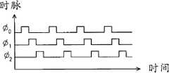
图6为图3的电容感测装置的电路示意图。在此,为了方便说明起见,图6仅示出感测电容C(n-1)及C(n+1)、待测电容C(n)+ΔC及差分感测电路118,并未示出其对应的开关单元。图7可作为图6的电容感测装置110动作时的时脉波形图。FIG. 6 is a schematic circuit diagram of the capacitive sensing device of FIG. 3 . Here, for the convenience of description, FIG. 6 only shows the sensing capacitors C(n-1) and C(n+1), the capacitor to be measured C(n)+ΔC and the
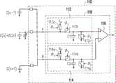
请参考图6及图7,在本实施例中,电容感测装置110是以感测电容C(n+1)的电容值作为测量待测电容C(n)+ΔC时的参考电容值。同时,电荷电压转换电路112及114例如是图6所示的电荷重分配电路的架构,而差值比较单元116例如是一比较器。Please refer to FIG. 6 and FIG. 7 , in this embodiment, the
在电容感测装置110动作时,电荷电压转换电路112及114的开关112a、112c、114a、114c受控于时脉信号Φ1,而电荷电压转换电路112及114的开关112b、114b受控于时脉信号Φ2。When the
因此,当时脉信号Φ1为高准位时,开关112a、112c、114a、114c为开启,系统电压Vcc分别对感测电容C(n+1)及待测电容C(n)+ΔC充电,而此时储存电容C1处于放电状态。在此,系统电压Vcc对感测电容C(n+1)及待测电容C(n)+ΔC所提供的充电电荷例如分别是Q1及Q2。Therefore, when the clock signalΦ1 is at a high level, the
之后,当时脉信号Φ2为高准位时,开关112b、114b为开启,使充电电荷Q1在时脉信号Φ2期间在感测电容C(n)、电容变化ΔC、储存电容C1间重新分配。因此,节点A的电压值为Q1/[C(n)+ΔC+C1],而Q1=Vcc×[C(n)+ΔC]。即是,此时电荷电压转换电路112将待测电容C(n)+ΔC的电容值转换为待测电压值,并输入至差值比较单元116的正输入端。Afterwards, when the clock signalΦ2 is at a high level, the
另一方面,类似于电荷电压转换电路112,电荷电压转换电路114同时也将感测电容C(n+1)的电容值转换为参考电压值,并输入至差值比较单元116的负输入端。因此,节点B的电压值为Q2/[C(n+1)+C2],而Q2=Vcc×C(n+1)。On the other hand, similar to the charge-to-
所以,在电容感测装置110完成一次时脉信号Φ1、Φ2后,差值比较单元116比较待测电压值及参考电压值的电压差值,并输出至后级电路,进而决定触控输入界面上的触碰位置。Therefore, after the
在本实施例中,差值比较单元116是以比较器为例,但本发明不以此为限。在另一实施例中,差值比较单元116例如是一差分放大器。当差值比较单元116为差分放大器时,其可比较并放大待测电压值及参考电压值的电压差值,并输出至后级电路,以提升判断触碰位置的准确率。另外,在另一实施例中,差值比较单元116也可以一积分器来实施。此时,积分器可比较并积分放大待测电压值及参考电压值的电压差值。In this embodiment, the
另外,在本实施例中,电容感测装置110是以感测电容C(n+1)的电容值作为测量待测电容C(n)+ΔC时的参考电容值。在另一实施例中,电容感测装置110也可以感测电容C(n-1)的电容值作为测量待测电容C(n)+ΔC时的参考电容值。此时,差值比较单元116所接收的参考电压值为Q2/[C(n-1)+C2],而Q2=Vcc×C(n-1)。在另一实施例中,电容感测装置110也可同时以感测电容C(n+1)、C(n-1)的电容值作为测量待测电容C(n)+ΔC时的参考电容值。此时,差值比较单元116所接收的参考电压值如下:In addition, in this embodiment, the
Q2/[(C(n+1)+C(n-1))/2+C2]Q2/[(C(n+1)+C(n-1))/2+C2]
而Q2=Vcc×[C(n+1)+C(n-1)]/2。And Q2=Vcc×[C(n+1)+C(n-1)]/2.
因此,在本发明的实施例中,电容感测装置可控制开关单元,使差分感测电路的参考输入端接收上述电容的至少其中一个所提供的参考电容值,以作为待测电容测量时的参考电容值。因此,电容感测装置可调整待测电容的测量参考值,使其测量结果较为准确,进而提升其测量效率。Therefore, in an embodiment of the present invention, the capacitance sensing device can control the switch unit so that the reference input terminal of the differential sensing circuit receives the reference capacitance value provided by at least one of the above-mentioned capacitances as the reference capacitance value when measuring the capacitance under test. Reference capacitor value. Therefore, the capacitance sensing device can adjust the measurement reference value of the capacitance to be measured to make the measurement result more accurate, thereby improving the measurement efficiency.
图8为图3的电容感测装置的另一电路示意图。同样地,为了方便说明起见,图8仅示出感测电容C(n-1)及C(n+1)、待测电容C(n)+ΔC及差分感测电路118’,并未示出其对应的开关单元。图7可作为图8的电容感测装置110’动作时的时脉波形图。FIG. 8 is another schematic circuit diagram of the capacitive sensing device of FIG. 3 . Similarly, for convenience of illustration, FIG. 8 only shows the sensing capacitors C(n-1) and C(n+1), the capacitor to be measured C(n)+ΔC and the differential sensing circuit 118', and does not show out the corresponding switch unit. FIG. 7 can be used as a clock waveform diagram when the capacitance sensing device 110' of FIG. 8 operates.
请参考图7及图8,在本实施例中,电容感测装置110’是以感测电容C(n+1)的电容值作为测量待测电容C(n)+ΔC时的参考电容值。同时,电荷电压转换电路112’及114’例如是图8所示的电荷重分配电路的架构,而差值比较单元116例如是一比较器。在此,图8的电容感测装置110’与图6的电容感测装置110主要的差异在于实现电荷电压转换电路的电荷重分配电路的架构不同。Please refer to FIG. 7 and FIG. 8. In this embodiment, the capacitance sensing device 110' uses the capacitance value of the sensing capacitance C(n+1) as the reference capacitance value when measuring the capacitance C(n)+ΔC to be measured. . Meanwhile, the charge-to-voltage conversion circuits 112' and 114' are, for example, the structure of the charge redistribution circuit shown in FIG. 8 , and the
在本实施例中,在电容感测装置110’动作时,电荷电压转换电路112’及114’的开关112d、112f、114d、114f受控于时脉信号Φ1,而电荷电压转换电路112’及114’的开关112e、114e受控于时脉信号Φ2。In this embodiment, when the capacitance sensing device 110' operates, the switches 112d, 112f, 114d, and 114f of the charge-to-voltage conversion circuits 112' and 114' are controlled by the clock signal Φ1 , and the charge-to-voltage conversion circuit 112' The switches 112e, 114e of and 114' are controlled by the clock signal Φ2 .
因此,当时脉信号Φ1为高准位时,开关112d、112f、114d、114f为开启,系统电压Vcc分别对电荷电压转换电路112’及114’内的储存电容充电,而此时感测电容C(n+1)及待测电容C(n)+ΔC为处于放电状态。在本实施例中,假设储存电容C3、C4的电容值相等,其值为Ci,但本发明并不限于此。在此,系统电压Vcc对储存电容C3、C4所提供的充电电荷例如是Qi。Therefore, when the clock signalΦ1 is at a high level, the switches 112d, 112f, 114d, and 114f are turned on, and the system voltage Vcc charges the storage capacitors in the charge-to-voltage conversion circuits 112' and 114' respectively, while the sensing capacitors C(n+1) and the capacitance under test C(n)+ΔC are in a discharge state. In this embodiment, it is assumed that the storage capacitors C3 and C4 have the same capacitance value as Ci, but the invention is not limited thereto. Here, the charge provided by the system voltage Vcc to the storage capacitors C3 and C4 is, for example, Qi.
之后,当时脉信号Φ2为高准位时,开关112e、114e为开启,使充电电荷Qi在时脉信号Φ2期间在待测电容C(n)+ΔC及储存电容Ci间重新分配。因此,节点A的电压值为Qi/[C(n)+ΔC+Ci],而Qi=Vcc×Ci。也即是,此时电荷电压转换电路112’将待测电容C(n)+ΔC的电容值转换为待测电压值,并输入至差值比较单元116的正输入端。Afterwards, when the clock signal Φ2 is at a high level, the switches 112e and 114e are turned on, so that the charge Qi is redistributed between the capacitor under test C(n)+ΔC and the storage capacitor Ci during the period of the clock signal Φ2. Therefore, the voltage value of node A is Qi/[C(n)+ΔC+Ci], and Qi=Vcc×Ci. That is, at this time, the charge-to-voltage conversion circuit 112' converts the capacitance value of the capacitance C(n)+ΔC to be measured into a voltage value to be measured, and inputs the value to the positive input terminal of the
另一方面,类似于电荷电压转换电路112’,电荷电压转换电路114’同时也将参考电容C(n+1)的电容值转换为参考电压值,并输入至差值比较单元116的负输入端。因此,节点B的电压值为Qi/[C(n+1)+Ci],而Qi=Vcc×Ci。On the other hand, similar to the charge-to-voltage conversion circuit 112', the charge-to-voltage conversion circuit 114' also converts the capacitance value of the reference capacitor C(n+1) into a reference voltage value, and inputs it to the negative input of the
所以,在电容感测装置110完成一次时脉信号Φ1、Φ2后,差值比较单元116比较待测电压值及参考电压值的电压差值,并输出至后级电路,进而决定触控输入界面上的触碰位置。Therefore, after the
在本实施例中,差值比较单元116是以比较器为例,但本发明不以此为限。在另一实施例中,差值比较单元116例如是差分放大器。当差值比较单元116为差分放大器时,其可比较并放大待测电压值及参考电压值的电压差值,并输出至后级电路,以提升判断触碰位置的准确率。另外,在另一实施例中,差值比较单元116也可以一积分器来实施。此时,积分器可比较并积分放大待测电压值及参考电压值的电压差值。In this embodiment, the
另外,在本实施例中,电容感测装置110’是以感测电容C(n+1)的电容值作为测量待测电容C(n)+ΔC时的参考电容值。在另一实施例中,电容感测装置110’也可以感测电容C(n-1)的电容值作为测量待测电容C(n)+ΔC时的参考电容值。此时,差值比较单元116所接收的参考电压值为Qi/[C(n-1)+Ci],而Qi=Vcc×Ci。在另一实施例中,电容感测装置110’也可同时以感测电容C(n+1)、C(n-1)的电容值作为测量待测电容C(n)+ΔC时的参考电容值。此时,差值比较单元116所接收的参考电压值为Qi/[(C(n+1)+C(n-1))/2+Ci],而Qi=Vcc×Ci。In addition, in this embodiment, the capacitance sensing device 110' uses the capacitance value of the sensing capacitance C(n+1) as a reference capacitance value when measuring the capacitance C(n)+ΔC to be measured. In another embodiment, the capacitance sensing device 110' can also sense the capacitance value of the capacitance C(n-1) as a reference capacitance value when measuring the capacitance C(n)+ΔC to be measured. At this time, the value of the reference voltage received by the
图9为本发明一实施例的电容感测装置的电路方块图。请参照图9,本实施例的电容感测装置910与图2A的电容感测装置110两者之间的差异例如在于电容感测装置910的差分感测电路918包括一电荷电压转换电路912、一电荷极性转换电路914及一差值比较单元916。FIG. 9 is a circuit block diagram of a capacitive sensing device according to an embodiment of the present invention. Please refer to FIG. 9, the difference between the
在本实施例中,电荷极性转换电路914用以接收待测电容C(n)+ΔC所对应的待测电荷,并在转换待测电荷的极性后,将其输出至电荷电压转换电路912。电荷电压转换电路912用以接收参考电容所对应的参考电荷及经过极性反转的待测电荷,其中经过极性反转的待测电荷与参考电荷的极性相反。In this embodiment, the charge
因此,经过极性反转的待测电荷与参考电荷在节点D会互相抵销,并产生一第二差值。所以,在本实施例中,第二差值为一电荷差值。之后,电荷电压转换电路912将电荷差值转换为电压差值,并输入差值比较单元916。Therefore, the polarity-reversed charge to be measured and the reference charge cancel each other at the node D, and a second difference is generated. Therefore, in this embodiment, the second difference is a charge difference. Afterwards, the charge-to-
在本实施例中,差值比较单元916例如是一积分器,但本发明并不限于此。因此,差值比较单元916将电压差值积分放大后,输出至后级电路,以决定触控输入界面上的触碰位置。In this embodiment, the
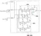
图10A为本发明第一实施例的电容感测装置的电路示意图。请参考图10A,本实施例的电容感测装置1010例如是应用在自容型的触控系统,但本发明并不限于此。在本实施例中,差分感测电路1018包括一电荷电压转换电路1012、一电荷极性转换电路1014及一差值比较单元1016。FIG. 10A is a schematic circuit diagram of the capacitive sensing device according to the first embodiment of the present invention. Please refer to FIG. 10A , the
为了方便说明起见,图10A仅示出感测电容C(n-1)及C(n+1)、待测电容C(n)+ΔC及差分感测电路1018,并未示出其对应的开关单元。图7可作为图10A的电容感测装置1010动作时的时脉波形图。For convenience of description, FIG. 10A only shows the sensing capacitors C(n-1) and C(n+1), the measured capacitor C(n)+ΔC and the
请参考图7及图10A,在本实施例中,电容感测装置1010是以感测电容C(n+1)的电容值作为测量待测电容C(n)+ΔC时的参考电容值,但本发明并不限于此。Please refer to FIG. 7 and FIG. 10A. In this embodiment, the
当时脉信号Φ1为高准位时,待测电容C(n)+ΔC所储存的电荷在待测电容C(n)+ΔC、电容C5、C7间重新分配,而参考电容C(n+1)所储存的电荷在感测电容C(n+1)、电容C6、C8间重新分配。之后,当时脉信号Φ2为高准位时,就待测输入端而言,储存在电容C7的待测电荷的极性会被反转,并提供节点E。例如,电容C7会将重新分配后的待测电荷的极性由正转负,以在节点E得到经过极性反转的待测电荷。同时,就参考输入端而言,储存在电容C8的参考电荷的极性不会被反转而是直接被提供至节点E。因此,经过极性反转的待测电荷与参考电荷的极性相反,且两者在节点E会互相抵销,并产生一电荷差值。同时,电荷电压转换电路1012将电荷差值转换为电压差值,并输入差值比较单元1016。When the clock signalΦ1 is at a high level, the charge stored in the capacitor under test C(n)+ΔC is redistributed among the capacitor under test C(n)+ΔC, capacitors C5 and C7, and the reference capacitor C(n+ΔC 1) The stored charge is redistributed among the sensing capacitor C(n+1), capacitors C6 and C8. Afterwards, when the clock signalΦ2 is at a high level, the polarity of the charge to be measured stored in the capacitor C7 will be reversed and provided to the node E as far as the input terminal to be measured is concerned. For example, the capacitor C7 will change the polarity of the redistributed charge to be measured from positive to negative, so as to obtain the charge to be measured at the node E after polarity reversal. Meanwhile, as far as the reference input terminal is concerned, the polarity of the reference charge stored in the capacitor C8 is not reversed but directly provided to the node E. Therefore, the polarity of the test charge and the reference charge after polarity inversion are opposite, and the two will cancel each other at the node E to generate a charge difference. At the same time, the charge-to-
所以,在电容感测装置1010完成一次时脉信号Φ1、Φ2后,差值比较单元1016的正输入端接收电压差值,并将其积分放大后,输出至后级电路,以决定触控输入界面上的触碰位置。Therefore, after the
在本实施例中,差值比较单元1016是以积分器为例,但本发明不以此为限。在另一实施例中,差值比较单元1016例如是差分放大器或比较器。In this embodiment, the
另外,在本实施例中,电容感测装置1010是以感测电容C(n+1)的电容值作为测量待测电容C(n)+ΔC时的参考电容值。在另一实施例中,电容感测装置1010也可以感测电容C(n-1)的电容值作为测量待测电容C(n)+ΔC时的参考电容值。在另一实施例中,电容感测装置1010也可同时以感测电容C(n+1)、C(n-1)的电容值作为测量待测电容C(n)+ΔC时的参考电容值。In addition, in this embodiment, the
此外,在本实施例中,电容感测装置1010是将待测电荷的极性反转,再与参考电荷抵销后得到电荷差值,但本发明并不限于此。在其他实施例中,电容感测装置1010也可将参考电荷的极性反转后,再与待测电荷抵销,以得到一电荷差值。之后,电荷电压转换电路再将电荷差值转换为电压差值,进而差值比较单元1016将电压差值积分放大后,输出至后级电路,以决定触控输入界面上的触碰位置。In addition, in this embodiment, the
图10B为本发明第二实施例的电容感测装置的电路示意图。请参考图10B,本实施例的电容感测装置1010’可以应用在自容型的触控系统,但本发明并不限于此。在本实施例中,电容感测装置1010’与图10A的电容感测装置1010的差异在于电荷电压转换电路1012’及电荷极性转换电路1014’的电路架构。FIG. 10B is a schematic circuit diagram of a capacitive sensing device according to a second embodiment of the present invention. Please refer to FIG. 10B , the capacitive sensing device 1010' of this embodiment can be applied in a self-capacitive touch system, but the present invention is not limited thereto. In this embodiment, the difference between the capacitive sensing device 1010' and the
为了方便说明起见,图10B仅示出感测电容C(n-1)及C(n+1)、待测电容C(n)+ΔC及差分感测电路1018’,并未示出其对应的开关单元。图10C为图10B的电容感测装置1010’动作时的时脉波形图。在本实施例中,每两个时脉讯号Φ0之间的期间可以是一感测期间。For convenience of description, FIG. 10B only shows the sensing capacitances C(n-1) and C(n+1), the capacitance to be measured C(n)+ΔC and the differential sensing circuit 1018', and does not show the corresponding switch unit. FIG. 10C is a clock waveform diagram when the capacitive sensing device 1010' in FIG. 10B operates. In this embodiment, the period between every two clock signalsΦ0 may be a sensing period.
图10C为又一电容感测装置动作时的时脉波形图,请参考图10B及图10C,在本实施例中,电容感测装置1010’是以感测电容C(n+1)的电容值作为测量待测电容C(n)+ΔC时的参考电容值,但本发明并不限于此。FIG. 10C is a clock waveform diagram when another capacitance sensing device operates. Please refer to FIG. 10B and FIG. 10C. The value is used as a reference capacitance value when measuring the capacitance C(n)+ΔC to be measured, but the present invention is not limited thereto.
当时脉信号Φ0为高准位时,待测电容C(n)+ΔC以及参考电容C(n+1)经由电荷电压转换电路1012’接地。也就是说,待测电容C(n)+ΔC以及参考电容C(n+1)所储存的电荷通过电荷电压转换电路1012’中对应于时脉讯号Φ0的开关放电,以清除在前一感测期间内待测电容C(n)+ΔC以及参考电容C(n+1)所储存的电荷。When the clock signalΦ0 is at a high level, the capacitor under test C(n)+ΔC and the reference capacitor C(n+1) are grounded via the charge-to-
接着,当时脉信号Φ1为高准位时,待测电容C(n)+ΔC所储存的电荷在待测电容C(n)+ΔC、电容C5、C7间重新分配,而参考电容C(n+1)所储存的电荷在感测电容C(n+1)、电容C6间重新分配。之后,当时脉信号Φ2为高准位时,就待测输入端而言,储存在电容C7的待测电荷的极性会被反转,并提供节点E。例如,电容C7会将重新分配后的待测电荷的极性由正转负,以在节点E得到经过极性反转的待测电荷。同时,就参考输入端而言,参考电容C(n+1)所储存的电荷会被传送至电容C8储存,而其参考电荷的极性不会被反转而是直接被提供至节点E。因此,经过极性反转的待测电荷与参考电荷的极性相反,且两者在节点E会互相抵销,并产生一电荷差值。同时,电荷电压转换电路1012’将电荷差值转换为电压差值,并输入差值比较单元1016。之后,当时脉信号Φ0为高准位时,电容感测装置1010’进行另一感测期间的操作。Next, when the clock signalΦ1 is at a high level, the charge stored in the capacitor under test C(n)+ΔC is redistributed among the capacitor under test C(n)+ΔC, capacitors C5 and C7, and the reference capacitor C( The charge stored in n+1) is redistributed between the sensing capacitor C(n+1) and the capacitor C6. Afterwards, when the clock signalΦ2 is at a high level, the polarity of the charge to be measured stored in the capacitor C7 will be reversed and provided to the node E as far as the input terminal to be measured is concerned. For example, the capacitor C7 will change the polarity of the redistributed charge to be measured from positive to negative, so as to obtain the charge to be measured at the node E after polarity reversal. Meanwhile, as far as the reference input terminal is concerned, the charge stored in the reference capacitor C(n+1) will be transferred to the capacitor C8 for storage, and the polarity of the reference charge will not be reversed but directly provided to the node E. Therefore, the polarities of the test charge and the reference charge after polarity inversion are opposite, and the two will cancel each other at the node E, and a charge difference will be generated. At the same time, the charge-to-
所以,在本实施例中,电容感测装置1010在每一感测期间内(即完成一次时脉信号Φ1、Φ2后),差值比较单元1016的正输入端接收电压差值,并将其积分放大后,输出至后级电路,以决定触控输入介面上的触碰位置。Therefore, in this embodiment, during each sensing period of the capacitance sensing device 1010 (that is, after completing one clock signal Φ1 , Φ2 ), the positive input terminal of the
在本实施例中,差值比较单元1016是以积分器为例,但本发明不以此为限。在另一实施例中,差值比较单元1016例如是差动放大器或比较器。In this embodiment, the
另外,在本实施例中,电容感测装置1010’是以感测电容C(n+1)的电容值作为量测待测电容C(n)+ΔC时的参考电容值。在另一实施例中,电容感测装置1010’也可以感测电容C(n-1)的电容值作为测量待测电容C(n)+ΔC时的参考电容值。在另一实施例中,电容感测装置1010’也可同时以感测电容C(n+1)、C(n-1)的电容值作为量测待测电容C(n)+ΔC时的参考电容值。In addition, in this embodiment, the capacitance sensing device 1010' uses the capacitance value of the sensing capacitance C(n+1) as a reference capacitance value when measuring the capacitance C(n)+ΔC to be measured. In another embodiment, the capacitance sensing device 1010' can also sense the capacitance value of the capacitance C(n-1) as a reference capacitance value when measuring the capacitance C(n)+ΔC to be measured. In another embodiment, the capacitance sensing device 1010' can also simultaneously use the capacitance values of the sensing capacitances C(n+1) and C(n-1) as the values when measuring the capacitance to be measured C(n)+ΔC Reference capacitor value.
此外,在本实施例中,电容感测装置1010’是将待测电荷的极性反转,再与参考电荷抵销后得到电荷差值,但本发明并不限于此。在其他实施例中,电容感测装置1010’也可将参考电荷的极性反转后,再与待测电荷抵销,以得到一电荷差值。之后,电荷电压转换电路再将电荷差值转换为电压差值,进而差值比较单元1016将电压差值积分放大后,输出至后级电路,以决定触控输入界面上的触碰位置。In addition, in this embodiment, the capacitance sensing device 1010' inverts the polarity of the charge to be measured, and then offsets the reference charge to obtain a charge difference, but the present invention is not limited thereto. In other embodiments, the capacitive sensing device 1010' can also invert the polarity of the reference charge, and then offset it with the charge to be measured to obtain a charge difference. Afterwards, the charge-to-voltage conversion circuit converts the charge difference into a voltage difference, and then the
图11为本发明第三实施例的电容感测装置的电路示意图。请参照图11,在本实施例中,电容感测装置1110的差分感测电路1118包括一电荷极性转换电路1112及一差值比较单元1116。在此,差值比较单元1116例如是一积分器。FIG. 11 is a schematic circuit diagram of a capacitive sensing device according to a third embodiment of the present invention. Please refer to FIG. 11 , in this embodiment, the
为了方便说明起见,图11仅示出感测电容C(n-1)及C(n+1)、待测电容C(n)+ΔC及差分感测电路1118,并未示出其对应的开关单元。图7可作为图11的电容感测装置1110动作时的时脉波形图。For convenience of description, FIG. 11 only shows the sensing capacitors C(n-1) and C(n+1), the capacitor to be measured C(n)+ΔC and the
请参考图7及图11,在本实施例中,电容感测装置1110是以感测电容C(n+1)的电容值作为测量待测电容C(n)+ΔC时的参考电容值,但本发明并不限于此。Please refer to FIG. 7 and FIG. 11. In this embodiment, the
当时脉信号Φ2为高准位时,系统电压Vcc分别对待测电容C(n)+ΔC及参考电容C(n+1)充电。之后,当时脉信号Φ1为高准位时,就待测电容而言,其所储存的电荷在时脉信号Φ1期间在待测电容C(n)+ΔC、电容C10间重新分配。接着,电容C10再对重新分配后的待测电荷作极性反转,以在时脉信号Φ2再次为高准位时,在节点F得到经过极性反转的待测电荷。另一方面,就参考电容而言,其所储存的电荷会被提供至节点F作为参考电荷。因此,经过极性反转的待测电荷与参考电荷在节点F会互相抵销,并产生一电荷差值。When the clock signalΦ2 is at a high level, the system voltage Vcc charges the capacitor to be measured C(n)+ΔC and the reference capacitor C(n+1) respectively. Afterwards, when the clock signalΦ1 is at a high level, as far as the capacitor under test is concerned, the stored charge is redistributed between the capacitor under test C(n)+ΔC and the capacitor C10 during the period of the clock signalΦ1 . Next, the capacitor C10 inverts the polarity of the redistributed charge to be measured, so that when the clock signalΦ2 is at a high level again, the charge to be measured with reversed polarity is obtained at the node F. On the other hand, as far as the reference capacitor is concerned, the stored charge will be provided to the node F as the reference charge. Therefore, the polarity-reversed charges to be measured and the reference charges will cancel each other at the node F, and a charge difference will be generated.
所以,在电容感测装置1110完成一次时脉信号Φ2、Φ1后,差值比较单元1116的正输入端接收电荷差值,并将其累积放大后,输出至后级电路,以决定触控输入界面上的触碰位置。Therefore, after the
在本实施例中,差值比较单元1116是以积分器为例,但本发明不以此为限。在另一实施例中,差值比较单元1116例如是差分放大器或比较器。In this embodiment, the
另外,在本实施例中,电容感测装置1110是以感测电容C(n+1)的电容值作为测量待测电容C(n)+ΔC时的参考电容值。在另一实施例中,电容感测装置1110也可以感测电容C(n-1)的电容值作为测量待测电容C(n)+ΔC时的参考电容值。在另一实施例中,电容感测装置1110也可同时以感测电容C(n+1)、C(n-1)的电容值作为测量待测电容C(n)+ΔC时的参考电容值。In addition, in this embodiment, the
此外,在本实施例中,电容感测装置1110是将待测电荷的极性反转,再与参考电荷抵销后得到电荷差值,但本发明并不限于此。在其他实施例中,电容感测装置1110也可先将参考电荷的极性反转后,再与待测电荷抵销,以得到电荷差值。差值比较单元1116将电荷差值积分放大并转换电压差值后,再输出至后级电路,以决定触控输入界面上的触碰位置。In addition, in this embodiment, the
图12A为本发明第四实施例的电容感测装置的电路示意图。请参照图12A,本实施例的电容感测装置1110’与图11的电容感测装置1110两者之间的差异例如在于差分感测电路1118’还包括一电荷非极性转换电路1114。FIG. 12A is a schematic circuit diagram of a capacitive sensing device according to a fourth embodiment of the present invention. Referring to FIG. 12A, the difference between the capacitive sensing device 1110' of this embodiment and the
为了方便说明起见,图12A仅示出感测电容C(n-1)及C(n+1)、待测电容C(n)+ΔC及差分感测电路1118’,并未示出其对应的开关单元。图7可作为图12A的电容感测装置1110’动作时的时脉波形图。For convenience of description, FIG. 12A only shows the sensing capacitors C(n-1) and C(n+1), the capacitor to be measured C(n)+ΔC and the differential sensing circuit 1118', and does not show the corresponding switch unit. FIG. 7 can be used as a clock waveform diagram when the capacitive sensing device 1110' in FIG. 12A operates.
请参考图7及图12A,在本实施例中,电容感测装置1110’是以感测电容C(n+1)的电容值作为测量待测电容C(n)+ΔC时的参考电容值,但本发明并不限于此。Please refer to FIG. 7 and FIG. 12A. In this embodiment, the capacitance sensing device 1110' uses the capacitance value of the sensing capacitance C(n+1) as the reference capacitance value when measuring the capacitance C(n)+ΔC to be measured. , but the present invention is not limited thereto.
当时脉信号Φ2为高准位时,系统电压Vcc分别对待测电容C(n)+ΔC及参考电容C(n+1)充电。之后,当时脉信号Φ1为高准位时,就待测电容而言,其所储存的电荷于时脉信号Φ1期间在待测电容C(n)+ΔC、电容C10间重新分配。接着,电容C10再对重新分配后的待测电荷作极性反转,以在节点G得到经过极性反转的待测电荷。同时,就参考电容而言,其所储存的电荷于时脉信号Φ1期间在感测电容C(n+1)、电容C12间重新分配。When the clock signalΦ2 is at a high level, the system voltage Vcc charges the capacitor to be measured C(n)+ΔC and the reference capacitor C(n+1) respectively. Afterwards, when the clock signalΦ1 is at a high level, as far as the capacitor under test is concerned, the stored charge is redistributed between the capacitor under test C(n)+ΔC and the capacitor C10 during the period of the clock signalΦ1 . Next, the capacitor C10 inverts the polarity of the redistributed charge to be measured, so as to obtain the charge to be measured with reversed polarity at the node G. Meanwhile, as far as the reference capacitor is concerned, the stored charges are redistributed between the sensing capacitor C(n+1) and the capacitor C12 during the period of the clock signalΦ1 .
应注意的是,在本实施例中,电容C12并不会反转参考电荷的极性,而是在时脉信号Φ2为高准位时,直接将参考电荷提供至节点G。因此,经过极性反转的待测电荷与参考电荷在时脉信号Φ2再次为高准位时,会在节点G互相抵销,并产生一电荷差值。It should be noted that, in this embodiment, the capacitor C12 does not reverse the polarity of the reference charge, but directly provides the reference charge to the node G when the clock signalΦ2 is at a high level. Therefore, when the clock signalΦ2 is at a high level again, the polarity-reversed charge to be measured and the reference charge will cancel each other at the node G and generate a charge difference.
所以,在电容感测装置1110’完成一次时脉信号Φ1、Φ2后,差值比较单元1116的正输入端接收电荷差值,并将其累积放大后,输出至后级电路,以决定触控输入界面上的触碰位置。Therefore, after the capacitive sensing device 1110' completes a clock signal Φ1 and Φ2 , the positive input terminal of the
在本实施例中,差值比较单元1116是以积分器为例,但本发明不以此为限。在另一实施例中,差值比较单元1116例如是差分放大器或比较器。In this embodiment, the
另外,在本实施例中,电容感测装置1110’是以感测电容C(n+1)的电容值作为测量待测电容C(n)+ΔC时的参考电容值。在另一实施例中,电容感测装置1110’也可以感测电容C(n-1)的电容值作为测量待测电容C(n)+ΔC时的参考电容值。在另一实施例中,电容感测装置1110’也可同时以感测电容C(n+1)、C(n-1)的电容值作为测量待测电容C(n)+ΔC时的参考电容值。In addition, in this embodiment, the capacitance sensing device 1110' uses the capacitance value of the sensing capacitance C(n+1) as a reference capacitance value when measuring the capacitance C(n)+ΔC to be measured. In another embodiment, the capacitance sensing device 1110' can also sense the capacitance value of the capacitance C(n-1) as a reference capacitance value when measuring the capacitance C(n)+ΔC to be measured. In another embodiment, the capacitance sensing device 1110' can also simultaneously use the capacitance values of the sensing capacitances C(n+1) and C(n-1) as a reference for measuring the capacitance to be measured C(n)+ΔC capacitance value.
此外,在本实施例中,电容感测装置1110’是将待测电荷的极性反转,再与参考电荷抵销后得到电荷差值,但本发明并不限于此。在其他实施例中,电容感测装置1110’也可先将参考电荷的极性反转后,再与待测电荷抵销,以得到电荷差值。差值比较单元1116将电荷差值积分放大并转换电压差值后,再输出至后级电路,以决定触控输入界面上的触碰位置。In addition, in this embodiment, the capacitance sensing device 1110' inverts the polarity of the charge to be measured, and then offsets the reference charge to obtain a charge difference, but the present invention is not limited thereto. In other embodiments, the capacitive sensing device 1110' may also invert the polarity of the reference charge first, and then offset it with the charge to be measured to obtain the charge difference. The
图12B为本发明第五实施例的电容感测装置的电路示意图。请参照图12B,本实施例的电容感测装置1110”与图12A的电容感测装置1110’两者之间的差异在于电荷非极性转换电路1114”的电路架构。12B is a schematic circuit diagram of a capacitive sensing device according to a fifth embodiment of the present invention. Referring to FIG. 12B , the difference between the
为了方便说明起见,图12B仅示出感测电容C(n-1)及C(n+1)、待测电容C(n)+ΔC及差分感测电路1118”,并未示出其对应的开关单元。图10C也可以作为图12B的电容感测装置1110”动作时的时脉波形图。在本实施例中,每两个时脉信号Φ0之间的期间可以是一感测期间。For convenience of illustration, FIG. 12B only shows the sensing capacitors C(n-1) and C(n+1), the capacitor to be measured C(n)+ΔC and the
请参考图10C及图12B,在本实施例中,电容感测装置1110”是以感测电容C(n+1)的电容值作为测量待测电容C(n)+ΔC时的参考电容值,但本发明并不限于此。Please refer to FIG. 10C and FIG. 12B. In this embodiment, the
当时脉信号Φ0为高准位时,系统电压Vcc分别对待测电容C(n)+ΔC及参考电容C(n+1)充电。之后,当时脉信号Φ1为高准位时,就待测电容而言,其所储存的电荷在时脉信号Φ1期间在待测电容C(n)+ΔC、电容C10间重新分配。接着,当时脉信号Φ2为高准位时,电容C10再对重新分配后的待测电荷作极性反转,以在节点G得到经过极性反转的待测电荷。同时,就参考电容而言,其所储存的电荷在时脉信号Φ2期间在感测电容C(n+1)、电容C12间重新分配。When the clock signalΦ0 is at a high level, the system voltage Vcc charges the capacitor to be measured C(n)+ΔC and the reference capacitor C(n+1) respectively. Afterwards, when the clock signalΦ1 is at a high level, as far as the capacitor under test is concerned, the stored charge is redistributed between the capacitor under test C(n)+ΔC and the capacitor C10 during the period of the clock signalΦ1 . Next, when the clock signalΦ2 is at a high level, the capacitor C10 inverts the polarity of the redistributed charge to be measured, so as to obtain the charge to be measured at the node G after polarity inversion. Meanwhile, as far as the reference capacitor is concerned, the stored charge is redistributed between the sensing capacitor C(n+1) and the capacitor C12 during the period of the clock signalΦ2 .
应注意的是,在本实施例中,电容C12并不会反转参考电荷的极性,而是在时脉信号Φ2为高准位时,直接将参考电荷提供至节点G。因此,经过极性反转的待测电荷与参考电荷在时脉信号Φ2为高准位时,会在节点G互相抵销,并产生一电荷差值。It should be noted that, in this embodiment, the capacitor C12 does not reverse the polarity of the reference charge, but directly provides the reference charge to the node G when the clock signalΦ2 is at a high level. Therefore, when the clock signalΦ2 is at a high level, the polarity-reversed charge to be measured and the reference charge will cancel each other at the node G and generate a charge difference.
所以,在本实施例中,电容感测装置1110”在每一感测期间内(即完成一次时脉信号Φ1、Φ2后),差值比较单元1116的正输入端接收电荷差值,并将其累积放大后,输出至后级电路,以决定触控输入界面上的触碰位置。Therefore, in this embodiment, during each sensing period of the
在本实施例中,差值比较单元1116是以积分器为例,但本发明不以此为限。在另一实施例中,差值比较单元1116例如是差动放大器或比较器。In this embodiment, the
另外,在本实施例中,电容感测装置1110”是以感测电容C(n+1)的电容值作为量测待测电容C(n)+ΔC时的参考电容值。在另一实施例中,电容感测装置1110”也可以感测电容C(n-1)的电容值作为量测待测电容C(n)+ΔC时的参考电容值。在另一实施例中,电容感测装置1110”也可同时以感测电容C(n+1)、C(n-1)的电容值作为量测待测电容C(n)+ΔC时的参考电容值。In addition, in this embodiment, the
此外,在本实施例中,电容感测装置1110”是将待测电荷的极性反转,再与参考电荷抵销后得到电荷差值,但本发明并不限于此。在其他实施例中,电容感测装置1110”也可先将参考电荷的极性反转后,再与待测电荷抵销,以得到电荷差值。差值比较单元1116将电荷差值积分放大并转换电压差值后,再输出至后级电路,以决定触控输入界面上的触碰位置。In addition, in this embodiment, the
图13为本发明一实施例的电容感测方法的步骤流程图。请同时参照图2A及图13,本实施例的电容感测方法包括如下步骤。首先,在步骤S1100中,提供多个开关单元SW1~SWi及一差分感测电路118,其中每一开关单元连接至对应的感测电容。接着,在步骤S1102中,接收感测电容的至少其中一个所提供的一待测电容值,例如接收待测电容C(n)+ΔC提供的待测电容值。之后,在步骤S1104中,接收感测电容的至少其中一个所提供的一参考电容值,例如接收感测电容C(n-1)或C(n+1)所提供的待测电容值。继之,在步骤S1106中,通过差分感测电路比较待测电容值与参考电容值,以产生对应于待测电容值与参考电容值的第一差值。FIG. 13 is a flow chart of steps of a capacitance sensing method according to an embodiment of the present invention. Please refer to FIG. 2A and FIG. 13 at the same time. The capacitance sensing method of this embodiment includes the following steps. First, in step S1100 , a plurality of switch units SW1 -SWi and a
另外,本发明的实施例的电容感测方法可以由图1~图12A实施例的叙述中获致足够的启示、建议与实施说明,因此不再赘述。In addition, the capacitive sensing method of the embodiment of the present invention can obtain sufficient enlightenment, suggestion and implementation description from the description of the embodiment in FIGS.
综上所述,在本发明的实施例中,电容感测装置可控制开关单元,使差分感测电路的参考输入端接收感测电容的至少其中一个所提供的参考电容值,以作为待测电容测量时的参考电容值。因此,电容感测装置可调整待测电容的测量参考值,使其测量结果较为准确,进而提升其测量效率。To sum up, in the embodiment of the present invention, the capacitance sensing device can control the switch unit so that the reference input terminal of the differential sensing circuit receives the reference capacitance value provided by at least one of the sensing capacitances as the capacitance to be tested. Reference capacitance value for capacitance measurement. Therefore, the capacitance sensing device can adjust the measurement reference value of the capacitance to be measured to make the measurement result more accurate, thereby improving the measurement efficiency.
最后应说明的是:以上实施例仅用以说明本发明的技术方案而非对其进行限制,尽管参照较佳实施例对本发明进行了详细的说明,本领域的普通技术人员应当理解:其依然可以对本发明的技术方案进行修改或者等同替换,而这些修改或者等同替换亦不能使修改后的技术方案脱离本发明技术方案的精神和范围。Finally, it should be noted that the above embodiments are only used to illustrate the technical solutions of the present invention and not to limit them. Although the present invention has been described in detail with reference to the preferred embodiments, those of ordinary skill in the art should understand that: it still Modifications or equivalent replacements can be made to the technical solutions of the present invention, and these modifications or equivalent replacements cannot make the modified technical solutions deviate from the spirit and scope of the technical solutions of the present invention.
Claims (27)
Translated fromChinesePriority Applications (1)
| Application Number | Priority Date | Filing Date | Title |
|---|---|---|---|
| CN 201010121353CN102163109B (en) | 2010-02-23 | 2010-02-23 | Touch sensing system, capacitance sensing device and capacitance sensing method |
Applications Claiming Priority (1)
| Application Number | Priority Date | Filing Date | Title |
|---|---|---|---|
| CN 201010121353CN102163109B (en) | 2010-02-23 | 2010-02-23 | Touch sensing system, capacitance sensing device and capacitance sensing method |
Publications (2)
| Publication Number | Publication Date |
|---|---|
| CN102163109A CN102163109A (en) | 2011-08-24 |
| CN102163109Btrue CN102163109B (en) | 2013-06-12 |
Family
ID=44464367
Family Applications (1)
| Application Number | Title | Priority Date | Filing Date |
|---|---|---|---|
| CN 201010121353Expired - Fee RelatedCN102163109B (en) | 2010-02-23 | 2010-02-23 | Touch sensing system, capacitance sensing device and capacitance sensing method |
Country Status (1)
| Country | Link |
|---|---|
| CN (1) | CN102163109B (en) |
Families Citing this family (10)
| Publication number | Priority date | Publication date | Assignee | Title |
|---|---|---|---|---|
| TWI465994B (en)* | 2011-12-09 | 2014-12-21 | Nuvoton Technology Corp | Touch sensing method and touch sensing apparatus using charge distribution manner |
| US10296137B2 (en) | 2012-09-17 | 2019-05-21 | Silicon Works Co., Ltd. | Control circuit and noise removing method for touch screen |
| CN103049158B (en)* | 2012-12-31 | 2016-03-16 | 深圳市汇顶科技股份有限公司 | A kind of touch detecting method of capacitive touch screen and system |
| US10031620B2 (en)* | 2016-06-30 | 2018-07-24 | Stmicroelectronics Asia Pacific Pte Ltd | Self-sensing touch panel |
| CN108064344B (en)* | 2017-11-20 | 2021-05-11 | 深圳市汇顶科技股份有限公司 | Differential circuit, capacitance detection circuit, touch detection device and terminal equipment |
| CN107991836A (en)* | 2017-12-18 | 2018-05-04 | 深圳奥比中光科技有限公司 | A kind of optical projection module containing safety monitoring function |
| TW202009676A (en)* | 2018-08-14 | 2020-03-01 | 瑞鼎科技股份有限公司 | Touch sensing device and touch sensing method |
| CN112881810B (en)* | 2021-01-22 | 2023-06-09 | 深圳市汇顶科技股份有限公司 | Detection circuit, chip and related electronic device |
| WO2022155878A1 (en)* | 2021-01-22 | 2022-07-28 | 深圳市汇顶科技股份有限公司 | Detection circuit, chip, and related electronic apparatus |
| CN113325322A (en)* | 2021-05-25 | 2021-08-31 | 珠海迈巨微电子有限责任公司 | Signal processing device, battery management device and battery management system |
Citations (2)
| Publication number | Priority date | Publication date | Assignee | Title |
|---|---|---|---|---|
| CN101571782A (en)* | 2009-06-16 | 2009-11-04 | 友达光电股份有限公司 | Touch panel and method for judging occurrence position of touch signal |
| CN101893972A (en)* | 2009-04-03 | 2010-11-24 | 统宝光电股份有限公司 | Sensing method and driving circuit of capacitive touch screen |
- 2010
- 2010-02-23CNCN 201010121353patent/CN102163109B/ennot_activeExpired - Fee Related
Patent Citations (2)
| Publication number | Priority date | Publication date | Assignee | Title |
|---|---|---|---|---|
| CN101893972A (en)* | 2009-04-03 | 2010-11-24 | 统宝光电股份有限公司 | Sensing method and driving circuit of capacitive touch screen |
| CN101571782A (en)* | 2009-06-16 | 2009-11-04 | 友达光电股份有限公司 | Touch panel and method for judging occurrence position of touch signal |
Non-Patent Citations (1)
| Title |
|---|
| Somashekar Bangalore Prakash, Pamela Abshire.A Fully Differential Rail-to-Rail Capacitance Measurement Circuit for Integrated Cell Sensing.《IEEE SENSORS 2007 Conference》.2007,第1444-1447页.* |
Also Published As
| Publication number | Publication date |
|---|---|
| CN102163109A (en) | 2011-08-24 |
Similar Documents
| Publication | Publication Date | Title |
|---|---|---|
| CN102163109B (en) | Touch sensing system, capacitance sensing device and capacitance sensing method | |
| TWI493416B (en) | Touch sensing system, capacitance sensing apparatus and capacitance sensing method thereof | |
| TWI507949B (en) | Touch sensing system, capacitance sensing circuit and capacitance sensing method thereof | |
| TWI438672B (en) | Sensing method and driving circuit of capacitive touch screen | |
| CN107449810B (en) | Capacitance measuring circuit, input device using the same, and electronic apparatus | |
| KR101916962B1 (en) | Capacitance voltage conversion circuit, input apparatus using the same, electronic instrument, and capacitance voltage conversion method | |
| US10788380B2 (en) | Apparatus for detecting capacitance, electronic device and apparatus for detecting force | |
| KR102337627B1 (en) | Capacitance detection circuit, touch device and terminal device | |
| US8659343B2 (en) | Calibration for mixed-signal integrator architecture | |
| CN109496273B (en) | Capacitance detection circuit, touch detection device and terminal equipment | |
| JP5191769B2 (en) | Capacity detection apparatus and method | |
| TWI411950B (en) | Touch panel | |
| JP7198586B2 (en) | CAPACITANCE DETECTION CIRCUIT, SEMICONDUCTOR DEVICE, INPUT DEVICE USING THE SAME, ELECTRONIC DEVICE, AND CAPACITY DETECTION METHOD | |
| US9146650B2 (en) | High resolution capacitance to code converter | |
| JP2011170617A (en) | Electrostatic capacity type touch sensor | |
| US20090225044A1 (en) | Determining touch on keys of touch sensitive input device | |
| US20140002115A1 (en) | Capacitance sensing method | |
| CN105580279B (en) | Multi-channel capacitive voltage divider scanning method and device | |
| TWI407357B (en) | Object sensing apparatus, touch sensing system and touch sensing method | |
| CN102043096A (en) | Capacitance measuring circuit and capacitance measuring method | |
| JP2011133964A (en) | Capacitance discrimination circuit and touch switch equipped with the same | |
| CN102156562A (en) | Object sensing device, touch sensing system and touch sensing method | |
| KR20210012132A (en) | High sensitivity touch sensor | |
| WO2021016991A1 (en) | Capacitance detection circuit, touch chip, and electronic device | |
| TWI408593B (en) | Capacitive touch panel and sensing apparatus thereof |
Legal Events
| Date | Code | Title | Description |
|---|---|---|---|
| C06 | Publication | ||
| PB01 | Publication | ||
| C10 | Entry into substantive examination | ||
| SE01 | Entry into force of request for substantive examination | ||
| C14 | Grant of patent or utility model | ||
| GR01 | Patent grant | ||
| CF01 | Termination of patent right due to non-payment of annual fee | ||
| CF01 | Termination of patent right due to non-payment of annual fee | Granted publication date:20130612 Termination date:20170223 |