CN102160180A - Image pickup device and solid-state image pickup element - Google Patents
Image pickup device and solid-state image pickup elementDownload PDFInfo
- Publication number
- CN102160180A CN102160180ACN2010800026389ACN201080002638ACN102160180ACN 102160180 ACN102160180 ACN 102160180ACN 2010800026389 ACN2010800026389 ACN 2010800026389ACN 201080002638 ACN201080002638 ACN 201080002638ACN 102160180 ACN102160180 ACN 102160180A
- Authority
- CN
- China
- Prior art keywords
- light
- splitting element
- photosensitive unit
- mentioned
- photosensitive
- Prior art date
- Legal status (The legal status is an assumption and is not a legal conclusion. Google has not performed a legal analysis and makes no representation as to the accuracy of the status listed.)
- Pending
Links
Images


Classifications
- H—ELECTRICITY
- H10—SEMICONDUCTOR DEVICES; ELECTRIC SOLID-STATE DEVICES NOT OTHERWISE PROVIDED FOR
- H10F—INORGANIC SEMICONDUCTOR DEVICES SENSITIVE TO INFRARED RADIATION, LIGHT, ELECTROMAGNETIC RADIATION OF SHORTER WAVELENGTH OR CORPUSCULAR RADIATION
- H10F39/00—Integrated devices, or assemblies of multiple devices, comprising at least one element covered by group H10F30/00, e.g. radiation detectors comprising photodiode arrays
- H10F39/10—Integrated devices
- H10F39/12—Image sensors
- H—ELECTRICITY
- H10—SEMICONDUCTOR DEVICES; ELECTRIC SOLID-STATE DEVICES NOT OTHERWISE PROVIDED FOR
- H10F—INORGANIC SEMICONDUCTOR DEVICES SENSITIVE TO INFRARED RADIATION, LIGHT, ELECTROMAGNETIC RADIATION OF SHORTER WAVELENGTH OR CORPUSCULAR RADIATION
- H10F39/00—Integrated devices, or assemblies of multiple devices, comprising at least one element covered by group H10F30/00, e.g. radiation detectors comprising photodiode arrays
- H10F39/80—Constructional details of image sensors
- H10F39/806—Optical elements or arrangements associated with the image sensors
- H—ELECTRICITY
- H10—SEMICONDUCTOR DEVICES; ELECTRIC SOLID-STATE DEVICES NOT OTHERWISE PROVIDED FOR
- H10F—INORGANIC SEMICONDUCTOR DEVICES SENSITIVE TO INFRARED RADIATION, LIGHT, ELECTROMAGNETIC RADIATION OF SHORTER WAVELENGTH OR CORPUSCULAR RADIATION
- H10F39/00—Integrated devices, or assemblies of multiple devices, comprising at least one element covered by group H10F30/00, e.g. radiation detectors comprising photodiode arrays
- H10F39/10—Integrated devices
- H10F39/12—Image sensors
- H10F39/199—Back-illuminated image sensors
- H—ELECTRICITY
- H10—SEMICONDUCTOR DEVICES; ELECTRIC SOLID-STATE DEVICES NOT OTHERWISE PROVIDED FOR
- H10F—INORGANIC SEMICONDUCTOR DEVICES SENSITIVE TO INFRARED RADIATION, LIGHT, ELECTROMAGNETIC RADIATION OF SHORTER WAVELENGTH OR CORPUSCULAR RADIATION
- H10F39/00—Integrated devices, or assemblies of multiple devices, comprising at least one element covered by group H10F30/00, e.g. radiation detectors comprising photodiode arrays
- H10F39/80—Constructional details of image sensors
- H10F39/805—Coatings
- H10F39/8053—Colour filters
- H—ELECTRICITY
- H10—SEMICONDUCTOR DEVICES; ELECTRIC SOLID-STATE DEVICES NOT OTHERWISE PROVIDED FOR
- H10F—INORGANIC SEMICONDUCTOR DEVICES SENSITIVE TO INFRARED RADIATION, LIGHT, ELECTROMAGNETIC RADIATION OF SHORTER WAVELENGTH OR CORPUSCULAR RADIATION
- H10F39/00—Integrated devices, or assemblies of multiple devices, comprising at least one element covered by group H10F30/00, e.g. radiation detectors comprising photodiode arrays
- H10F39/80—Constructional details of image sensors
- H10F39/806—Optical elements or arrangements associated with the image sensors
- H10F39/8063—Microlenses
- H—ELECTRICITY
- H04—ELECTRIC COMMUNICATION TECHNIQUE
- H04N—PICTORIAL COMMUNICATION, e.g. TELEVISION
- H04N2209/00—Details of colour television systems
- H04N2209/04—Picture signal generators
- H04N2209/041—Picture signal generators using solid-state devices
- H04N2209/042—Picture signal generators using solid-state devices having a single pick-up sensor
- H04N2209/047—Picture signal generators using solid-state devices having a single pick-up sensor using multispectral pick-up elements
Landscapes
- Solid State Image Pick-Up Elements (AREA)
- Color Television Image Signal Generators (AREA)
- Transforming Light Signals Into Electric Signals (AREA)
Abstract
Translated fromChineseDescription
Translated fromChinese技术领域technical field
本发明涉及固体摄像元件的高灵敏度化以及彩色化的技术。The present invention relates to techniques for increasing the sensitivity and coloring of solid-state imaging elements.
背景技术Background technique
近年来,对使用CCD或CMOS等的固体摄像元件(以下,有时也称为“摄像元件”)的数字照相机或数字摄像机的高功能化、高性能化引人注目。特别是由于半导体制造技术的快速进步,摄像元件中的像素结构的细微化不断发展。其结果是,正力图实现摄像元件的像素以及驱动电路的高集成化以及摄像元件的高性能化。特别是最近,还开发出了使用不在形成固体摄像元件的布线层的一面(表面),而在背面侧接收光的背面照射型(Backside illumination)的摄像元件的照相机,其高灵敏度特性等备受关注。另一方面,随着摄像元件的多像素化,1个像素所接收的光量降低,因此,产生照相机灵敏度降低的问题。In recent years, attention has been paid to increasing the functionality and performance of digital still cameras and digital video cameras using solid-state imaging elements such as CCDs and CMOSs (hereinafter, sometimes referred to as "imaging elements"). In particular, the miniaturization of the pixel structure in the imaging element is progressing due to the rapid progress of the semiconductor manufacturing technology. As a result, efforts have been made to achieve higher integration of pixels and drive circuits of the imaging element and higher performance of the imaging element. Especially recently, a camera using a backside illumination type imaging element that receives light on the back side instead of on the side (surface) where the wiring layer of the solid-state imaging element is formed has been developed. focus on. On the other hand, since the amount of light received by one pixel decreases with the increase in the number of pixels of the imaging element, there is a problem that the sensitivity of the camera decreases.
照相机的灵敏度降低除了多像素化之外,使用用于色分离的滤色器也是一个原因。由于通常的滤色器吸收所利用的颜色分量以外的光,因此,在使用这种滤色器的情况下,照相机的光利用率会降低。作为具体的例子,在使用拜耳型的滤色器的彩色照相机中,由于在摄像元件的各光敏部上配置了使有机颜料成为色素的减色型的滤色器,因此,光利用率相当低。拜耳型的滤色器排列是将红(R)1要素、绿(G)2要素和蓝(B)1要素作为基本构成的排列。R滤光器使R光透过,而吸收G光、B光。G滤光器使G光透过,而吸收R光、B光。B滤光器使B光透过,而吸收R光、G光。即,透过滤色器的光是RGB三种颜色中的一种颜色,其他的两种颜色被滤色器吸收。因此,被利用的光是入射光的大约1/3。In addition to multi-pixelation, the reduction in the sensitivity of the camera is also caused by the use of color filters for color separation. Since a general color filter absorbs light other than the used color components, the use of such a color filter reduces the light utilization efficiency of the camera. As a specific example, in a color camera using a Bayer-type color filter, since a subtractive color filter in which an organic pigment is used as a pigment is arranged on each photosensitive part of the imaging element, the light utilization efficiency is quite low. . The Bayer-type color filter array is an array basically composed of one element of red (R), two elements of green (G), and one element of blue (B). The R filter transmits R light and absorbs G light and B light. The G filter transmits G light and absorbs R light and B light. The B filter transmits B light and absorbs R light and G light. That is, the light transmitted through the color filter is one of the three colors of RGB, and the other two colors are absorbed by the color filter. Therefore, the light utilized is about 1/3 of the incident light.
为了解决该灵敏度降低的问题,专利文献1中公开了通过在摄像元件的光接收部安装微透镜阵列来增加接收的光量的方法。根据该方法,通过用微透镜聚光能实质上提高光开口率。现在,该方法用于几乎所有的固体摄像元件中。虽然使用该方法可以提高实质上的开口率,但其并不能解决滤色器造成的光利用率降低的问题。In order to solve this problem of decreased sensitivity,
因此,作为同时解决光利用率降低和灵敏度降低的问题的方法,专利文献2公开了具有将多层膜的滤色器(分色镜)和微透镜组合,从而最大限度地获取光的结构的摄像元件。在该摄像元件中使用不吸收光而选择性地使特定波段的光透过并将其他波段的光反射的多个分色镜。各分色镜只将所需要的光选择性地入射到对应的光敏部上,而使其他的光透过。图8显示了专利文献2公开的摄像元件的剖视图。Therefore, as a method for simultaneously solving the problems of lowered light utilization efficiency and lowered sensitivity,
根据图8所示的固体摄像元件,入射到聚光微透镜11的光在通过内透镜12被调整光束之后,入射到第1分色镜13。第1分色镜13虽然使红色(R)光透过,但是将其他颜色的光反射。第2分色镜14虽然将绿色(G)光反射,但是使其他颜色的光透过。第3分色镜15虽然将蓝色(B)光反射,但是使其他颜色的光透过。透过第1分色镜13的光入射到正下方的光敏单元2。由第1分色镜13反射的光入射到相邻的第2分色镜14。第2分色镜14反射绿色(G)光,透过蓝色(B)光。由第2分色镜14反射的绿色的光入射到正下方的光敏单元2。透过第2分色镜14的蓝色光被第3分色镜15反射,入射到正下方的光敏单元2。根据这种固体摄像元件,入射到聚光微透镜11的可见光不会被滤色器吸收,RGB各种颜色的光会被光敏单元毫无浪费地检测。According to the solid-state imaging device shown in FIG. 8 , the light incident on the
除了上述现有技术,在专利文献3中公开了能通过使用微棱镜来防止光损失的摄像元件。该摄像元件具有用不同的光敏单元分别接收通过微棱镜而分离成红色、绿色和蓝色的光的结构。在使用这种摄像元件的情况下也能防止光损失。In addition to the prior art described above, an imaging element capable of preventing light loss by using microprisms is disclosed in
但是,在专利文献2、3中公开的技术中,使用多少分色镜或分光的数量有多少,就需要设置多少光敏单元。例如,为了接收红色、绿色和蓝色的光,与使用滤色器的情况下的光敏单元的数量相比必须增加3倍的光敏单元。这是一个需要解决的课题。However, in the technologies disclosed in
另一方面,在专利文献4中公开了一种从摄像元件的两侧获取光的与上述现有技术不同的技术。在该技术中,配置光学系统以及滤色器,以使可见光和非可见光(红外线或紫外线)分别入射到摄像元件的表面一侧和背面一侧。根据该技术,虽然能用一个摄像元件获取可见光以及非可见光的图像,但该技术并不是用来解决由滤色器引起的光利用率降低的问题。On the other hand,
另外,在专利文献5中公开了一种彩色化技术,该彩色化技术通过使用与各光敏单元对应配置的微棱镜等的构造物(分光要素),可无需大规模地增加光敏单元就能提高光利用率。根据该技术,由于与光敏单元对应配置的分光要素的缘故,光会根据波段而入射到不同的光敏单元。各个光敏单元从多个分光要素接收不同波段的分量被重叠的光。其结果是,能根据使用从各光敏单元输出的光电转换信号的信号运算来生成颜色信号。In addition,
专利文献1:JP特开昭59-90467号公报Patent Document 1: JP Unexamined Patent Publication No. 59-90467
专利文献2:JP特开2000-151933号公报Patent Document 2: JP Unexamined Publication No. 2000-151933
专利文献3:JP特开2001-309395号公报Patent Document 3: JP-A-2001-309395
专利文献4:JP特开2008-072423号公报Patent Document 4: JP Unexamined Patent Application Publication No. 2008-072423
专利文献5:国际公开第2009/153937号Patent Document 5: International Publication No. 2009/153937
在现有技术中,如果使用光吸收型的滤色器,则虽然能不用大幅度地增加光敏单元,但是光利用率会变低。另一方面,如果使用光选择透过型的滤色器(分色镜)或微棱镜,则虽然光利用率很高,但是必须大幅度地增加光敏单元。In the prior art, if a light-absorbing color filter is used, although it is not necessary to greatly increase the number of photosensitive units, the light utilization efficiency will become lower. On the other hand, if a light selective transmission type color filter (dichroic mirror) or a microprism is used, although the light utilization efficiency is high, it is necessary to greatly increase the photosensitive unit.
另一方面,根据专利文献5公开的技术,从理论上来讲,的确能获得光利用率高的彩色图像,但是,与摄像元件的像素对应且高密度地配置微棱镜等构造物是具有很高难度的。On the other hand, according to the technology disclosed in
发明内容Contents of the invention
因此,本发明的目的是提供一种实现可分光的构造物的低密度化,并且无需大幅度地增加光敏单元就能进行颜色分离的彩色摄像技术。Therefore, it is an object of the present invention to provide a color imaging technology capable of reducing the density of light-splitting structures and performing color separation without greatly increasing the number of photosensitive cells.
本发明的摄像装置具有固体摄像元件和在上述固体摄像元件的摄像面上成像的光学系统。上述固体摄像元件具有:半导体层,其具有第1面以及位于上述第1面的相反侧的第2面;光敏单元阵列,其形成在上述半导体层中,且从上述第1面一侧以及上述第2面一侧接收光;和分光要素阵列,其与上述光敏单元阵列相对置地形成在上述第1面一侧以及上述第2面一侧中的至少一侧。上述光敏单元阵列具有分别包括第1光敏单元以及第2光敏单元的多个单元块。上述分光要素阵列使不同波段的光入射到上述第1光敏单元以及上述第2光敏单元。An imaging device according to the present invention includes a solid-state imaging element and an optical system for forming an image on an imaging surface of the solid-state imaging element. The above-mentioned solid-state imaging device has: a semiconductor layer having a first surface and a second surface on the opposite side of the first surface; receiving light on the side of the second surface; and an array of light-splitting elements formed on at least one of the side of the first surface and the side of the second surface opposite to the array of photosensitive elements. The above-mentioned photosensitive unit array has a plurality of unit blocks respectively including a first photosensitive unit and a second photosensitive unit. The light-splitting element array allows light of different wavelength bands to enter the first photosensitive unit and the second photosensitive unit.
在一实施方式中,上述光学系统将光的各一半分别入射到上述第1面以及上述第2面。In one embodiment, the optical system makes each half of the light incident on the first surface and the second surface.
在一个实施方式中,上述分光要素阵列具有:第1分光要素阵列,其与上述光敏单元阵列相对置地形成在上述第1面一侧;和第2分光要素,其与上述光敏单元阵列相对置地形成在上述第2面一侧。上述第1分光要素阵列使第1波段的光入射到上述第1光敏单元;使上述第1波段以外的光入射到上述第2光敏单元。上述第2分光要素阵列使与上述第1波段不同的第2波段的光入射到上述第1光敏单元;使上述第2波段以外的光入射到上述第2光敏单元。In one embodiment, the array of light-splitting elements includes: a first array of light-splitting elements formed on the side of the first surface opposite to the array of photosensitive cells; and a second array of light-splitting elements formed opposite to the array of photosensitive cells On the side of the second surface mentioned above. The first light-splitting element array makes light in the first wavelength band incident on the first photosensitive unit; makes light outside the first wavelength band incident on the second photosensitive unit. The second light-splitting element array allows light in a second wavelength band different from the first wavelength band to enter the first photosensitive unit; and allows light other than the second wavelength band to enter the second photosensitive unit.
在一个实施方式中,在将入射光分类成第1颜色分量的光、第2颜色分量的光以及第3颜色分量的光时,上述第1分光要素阵列具有第1分光要素,该第1分光要素是与上述第1光敏单元对应配置的第1分光要素,并使上述第1颜色分量的光入射到上述第1光敏单元,使上述第2以及第3颜色分量的光入射到上述第2光敏单元。另外,上述第2分光要素阵列具有第2分光要素,该第2分光要素是与上述第2光敏单元对应配置的第2分光要素,并使上述第2颜色分量的光入射到上述第1光敏单元,使上述第1以及第3颜色分量的光入射到上述第2光敏单元。In one embodiment, when the incident light is classified into the light of the first color component, the light of the second color component and the light of the third color component, the above-mentioned first light-splitting element array has a first light-splitting element, and the first light-splitting element The element is a first light-splitting element arranged corresponding to the first photosensitive unit, and makes the light of the first color component incident on the first photosensitive unit, and makes the light of the second and third color components incident on the second photosensitive unit. unit. In addition, the above-mentioned second light-splitting element array has a second light-splitting element, and the second light-splitting element is a second light-splitting element arranged corresponding to the above-mentioned second photosensitive unit, and makes the light of the above-mentioned second color component incident on the above-mentioned first photosensitive unit. , making the light of the first and third color components incident on the second photosensitive unit.
在一个实施方式中,在将入射光分类成第1颜色分量的光、第2颜色分量的光以及第3颜色分量的光时,上述第1分光要素阵列具有第1分光要素,该第1分光要素是与上述第1光敏单元对应配置的第1分光要素,并使上述第1颜色分量的光入射到上述第1光敏单元,使上述第2颜色分量的光入射到上述第2光敏单元,使上述第3颜色分量的光入射到包括在相邻的第1相邻单元块中的1个光敏单元。另外,上述第2分光要素阵列具有第2分光要素,该第2分光要素是与上述第2光敏单元对应配置的第2分光要素,并使上述第3颜色分量的光的各一半分别入射到上述第1光敏单元以及包括在相邻的第2相邻单元块中的1个光敏单元,使上述第1以及第2颜色分量的光入射到上述第2光敏单元。上述第1光敏单元接收从上述第1分光要素入射的上述第1颜色分量的光、和从上述第2分光要素以及包括在上述第1相邻单元块中的分光要素入射的上述第3颜色分量的光。上述第2光敏单元接收从上述第1分光要素入射的上述第2颜色分量的光、从包括在上述第2相邻单元块中的分光要素入射的上述第3颜色分量的光、以及从上述第2分光要素入射的上述第1以及第2颜色分量的光。In one embodiment, when the incident light is classified into the light of the first color component, the light of the second color component and the light of the third color component, the above-mentioned first light-splitting element array has a first light-splitting element, and the first light-splitting element The element is a first light-splitting element arranged corresponding to the first photosensitive unit, and makes the light of the first color component incident on the first photosensitive unit, and makes the light of the second color component incident on the second photosensitive unit, so that The light of the third color component is incident on one photosensitive cell included in the adjacent first adjacent cell block. In addition, the above-mentioned second light-splitting element array has a second light-splitting element, and the second light-splitting element is a second light-splitting element arranged correspondingly to the above-mentioned second photosensitive unit, and makes each half of the light of the above-mentioned third color components incident on the above-mentioned The first photosensitive cell and one photosensitive cell included in the adjacent second adjacent cell block make the light of the first and second color components incident on the second photosensitive cell. The first photosensitive unit receives the light of the first color component incident from the first light-splitting element, and the third color component incident from the second light-splitting element and the light-splitting element included in the first adjacent unit block. of light. The second photosensitive unit receives the light of the second color component incident from the first light-splitting element, the light of the third color component incident from the light-splitting element included in the second adjacent unit block, and the light of the third color component incident from the first light-splitting element. The light of the first and second color components incident on the 2 spectroscopic elements.
在一个实施方式中,各单元块包括第3光敏单元以及第4光敏单元,上述第1分光要素阵列具有第3分光要素,该第3分光要素是与上述第3光敏单元对应配置的第3分光要素,并使上述第1颜色分量的光入射到上述第3光敏单元,使上述第2以及第3颜色分量的光入射到上述第4光敏单元。上述第2分光要素阵列具有第4分光要素,该第4分光要素是与上述第4光敏单元对应配置的第4分光要素,并使上述第2颜色分量的光入射到上述第3光敏单元,使上述第1以及第3颜色分量的光入射到上述第4光敏单元。In one embodiment, each unit block includes a third photosensitive unit and a fourth photosensitive unit, the first light-splitting element array has a third light-splitting element, and the third light-splitting element is a third light-splitting element corresponding to the third photosensitive unit. elements, and make the light of the first color component incident on the third photosensitive unit, and make the light of the second and third color components incident on the fourth photosensitive unit. The above-mentioned second light-splitting element array has a fourth light-splitting element, and the fourth light-splitting element is a fourth light-splitting element correspondingly arranged with the above-mentioned fourth photosensitive unit, and makes the light of the above-mentioned second color component incident on the above-mentioned third photosensitive unit, so that The light of the first and third color components is incident on the fourth photosensitive unit.
在一个实施方式中,各单元块包括第3光敏单元以及第4光敏单元,上述第1分光要素阵列具有第3分光要素,该第3分光要素是与上述第3光敏单元对应配置的第3分光要素,并使上述第1颜色分量的光入射到上述第3光敏单元,使上述第3颜色分量的光入射到上述第4光敏单元,使上述第2颜色分量的光入射到包括在上述第2相邻单元块中的1个光敏单元。上述第2分光要素阵列具有第4分光要素,该第4分光要素是与包括在各单元块中的上述第4光敏单元对应配置的第4分光要素,并使上述第2颜色分量的光的各一半分别入射到上述第3光敏单元以及包括在上述第1相邻单元块中的1个光敏单元,使上述第1以及第3颜色分量的光入射到上述第4光敏单元。上述第3光敏单元接收从上述第3分光要素入射的上述第1颜色分量的光、和从上述第4分光要素以及包括在上述第2相邻单元要素中的分光要素入射的上述第2颜色分量的光。上述第4光敏单元接收从上述第3分光要素入射的上述第3波段的光、从包括在上述第1相邻单元要素中的分光要素入射的上述第2波段的光、以及从上述第4分光要素入射的上述第1波段以及上述第3波段的光。In one embodiment, each unit block includes a third photosensitive unit and a fourth photosensitive unit, the first light-splitting element array has a third light-splitting element, and the third light-splitting element is a third light-splitting element corresponding to the third photosensitive unit. elements, and make the light of the first color component incident on the third photosensitive unit, make the light of the third color component incident on the fourth photosensitive unit, and make the light of the second color component incident on the photosensitive unit included in the second 1 photosensitive unit in adjacent unit block. The above-mentioned second light-splitting element array has a fourth light-splitting element, and the fourth light-splitting element is a fourth light-splitting element that is arranged correspondingly to the above-mentioned fourth photosensitive unit included in each unit block, and makes each light of the above-mentioned second color component Half of them are respectively incident on the third photosensitive unit and one photosensitive unit included in the first adjacent unit block, so that the light of the first and third color components is incident on the fourth photosensitive unit. The third photosensitive unit receives the light of the first color component incident from the third light-splitting element, and the second color component incident from the fourth light-splitting element and the light-splitting element included in the second adjacent unit element. of light. The above-mentioned 4th photosensitive unit receives the light of the above-mentioned 3rd waveband incident from the above-mentioned 3rd light-splitting element, the light of the above-mentioned 2nd waveband incident from the light-splitting element included in the above-mentioned 1st adjacent unit element, and the light from the above-mentioned 4th light-splitting element. Elements incident on the above-mentioned first wavelength band and the above-mentioned light of the third wavelength band.
在一个实施方式中,上述第1光敏单元、上述第2光敏单元、上述第3光敏单元以及上述第4光敏单元配置成行列式,上述第1光敏单元与上述第2光敏单元相邻,上述第3光敏单元与上述第4光敏单元相邻。In one embodiment, the first photosensitive unit, the second photosensitive unit, the third photosensitive unit, and the fourth photosensitive unit are arranged in a determinant, the first photosensitive unit is adjacent to the second photosensitive unit, and the second photosensitive unit is adjacent to the second photosensitive unit. The 3rd photosensitive unit is adjacent to the aforementioned 4th photosensitive unit.
在一个实施方式中,上述固体摄像元件具有:第1微透镜阵列,其与上述第1分光要素阵列相对置地形成,并包括分别聚光于上述第1分光要素以及上述第3分光要素的多个微透镜;和第2微透镜阵列,其与上述第2分光要素阵列相对置地形成,并包括分别聚光于上述第2分光要素以及上述第4分光要素的多个微透镜。In one embodiment, the solid-state imaging device has: a first microlens array formed to face the first beam-splitting element array, and includes a plurality of light-splitting elements respectively focused on the first beam-splitting element and the third beam-splitting element. a microlens; and a second microlens array formed opposite to the second light splitting element array, and including a plurality of microlenses respectively focused on the second light splitting element and the fourth light splitting element.
在一个实施方式中,摄像装置还具有信号处理部,上述信号处理部根据从上述第1光敏单元以及上述第2光敏单元分别输出的光电转换信号生成一种颜色信号。In one embodiment, the imaging device further includes a signal processing unit that generates one color signal based on the photoelectric conversion signals respectively output from the first photosensitive unit and the second photosensitive unit.
在一个实施方式中,上述信号处理部根据从上述第1光敏单元、上述第2光敏单元、上述第3光敏单元以及上述第4光敏单元分别输出的光电转换信号生成三种颜色信号。In one embodiment, the signal processing unit generates three color signals based on photoelectric conversion signals respectively output from the first photosensitive unit, the second photosensitive unit, the third photosensitive unit, and the fourth photosensitive unit.
本发明的固体摄像元件具有:半导体层,其包括第1面以及位于上述第1面的相反侧的第2面;光敏单元阵列,其形成在上述半导体层中,且从上述第1面一侧以及上述第2面一侧接收光;和分光要素阵列,其与上述光敏单元阵列相对置地形成在上述第1面一侧以及上述第2面一侧中的至少一侧上。上述光敏单元阵列具有分别包括第1光敏单元以及第2光敏单元的多个单元块。上述分光要素阵列使不同波段的光入射到上述第1光敏单元以及上述第2光敏单元。The solid-state imaging device of the present invention has: a semiconductor layer including a first surface and a second surface on the opposite side of the first surface; and the side of the second surface receiving light; and an array of light-splitting elements formed on at least one of the side of the first surface and the side of the second surface opposite to the array of photosensitive elements. The above-mentioned photosensitive unit array has a plurality of unit blocks respectively including a first photosensitive unit and a second photosensitive unit. The light-splitting element array allows light of different wavelength bands to enter the first photosensitive unit and the second photosensitive unit.
(发明效果)(invention effect)
根据本发明的固体摄像元件以及摄像装置,由于光敏单元阵列从表面侧以及背面侧接收光,并且使用不吸收光的分光要素阵列,因此,能提高光利用率。另外,如果在两面侧配置分光要素阵列,则能减小每一面的分光要素的密度,使制造变得容易。而且,通过恰当地配置各分光要素能获得三种颜色分量的信号。According to the solid-state imaging device and imaging device of the present invention, since the photosensitive cell array receives light from the front side and the back side, and uses a light-splitting element array that does not absorb light, light utilization efficiency can be improved. In addition, if the light-splitting element arrays are arranged on both sides, the density of the light-splitting elements on each side can be reduced, which facilitates manufacturing. Furthermore, signals of three color components can be obtained by properly arranging the respective spectroscopic elements.
附图说明Description of drawings
图1是表示本发明的摄像装置的概略构成的框图。FIG. 1 is a block diagram showing a schematic configuration of an imaging device of the present invention.
图2A是表示本发明的摄像元件的结构的一个例子的示意图。FIG. 2A is a schematic diagram showing an example of the structure of the imaging device of the present invention.
图2B是表示本发明的摄像元件的其他例子的示意图。FIG. 2B is a schematic diagram showing another example of the imaging device of the present invention.
图2C是表示本发明的摄像元件的另外一个例子的示意图。FIG. 2C is a schematic diagram showing another example of the imaging device of the present invention.
图3是表示本发明的第1实施方式的摄像装置的整体构成的框图。3 is a block diagram showing the overall configuration of the imaging device according to the first embodiment of the present invention.
图4是表示本发明的第1实施方式的摄像装置的光学系统的构成的示意图。4 is a schematic diagram showing the configuration of the optical system of the imaging device according to the first embodiment of the present invention.
图5A是表示本发明的第1实施方式的像素结构的一个例子的图。5A is a diagram showing an example of a pixel structure according to the first embodiment of the present invention.
图5B是表示本发明的第1实施方式的像素结构的其他例子的图。5B is a diagram showing another example of the pixel structure of the first embodiment of the present invention.
图6A是表示本发明的第1实施方式的摄像元件的基本结构的俯视图。FIG. 6A is a plan view showing the basic configuration of the imaging element according to the first embodiment of the present invention.
图6B是表示图6A中的AA’线剖视图。Fig. 6B is a sectional view taken along line AA' in Fig. 6A.
图6C是表示图6A中的BB’线剖视图。Fig. 6C is a sectional view taken along line BB' in Fig. 6A.
图7A是表示本发明的第2实施方式的摄像元件的基本结构的俯视图。7A is a plan view showing a basic configuration of an imaging element according to a second embodiment of the present invention.
图7B是图7A中的CC’线剖视图。Fig. 7B is a sectional view taken along line CC' in Fig. 7A.
图7C是图7A中的DD’线剖视图。Fig. 7C is a sectional view taken along line DD' in Fig. 7A.
图8是使用微透镜和多层膜滤色器(分色镜)的以往的固体摄像元件的剖视图。8 is a cross-sectional view of a conventional solid-state imaging device using a microlens and a multilayer color filter (dichroic mirror).
具体实施方式Detailed ways
在对本发明的优选实施方式进行说明之前,首先说明本发明的基本原理。并且,在以下的说明中,有时会将对波段或者颜色分量不同的光进行空间性分离称为“分光”。另外,在以下的说明中,2个光的波段不同是指包含在2个光中的主要颜色分量不同。例如,如果一种光为品红色(Mg)光,另一种为红色(R)光,则前者的主要颜色分量为红色(R)以及蓝色(B),与作为后者的主要颜色分量的红色(R)不同。因此,品红色光和红色光具有不同的波段。Before describing the preferred embodiment of the present invention, the basic principle of the present invention will be described first. In addition, in the following description, spatial separation of light having different wavelength bands or color components may be referred to as "spectral separation". In addition, in the following description, the fact that the two lights have different wavelength bands means that the main color components included in the two lights are different. For example, if one light is magenta (Mg) light and the other is red (R) light, the main color components of the former are red (R) and blue (B), and the main color components of the latter are red (R) and blue (B). The red (R) is different. Therefore, magenta light and red light have different wavelength bands.
图1是表示本发明的摄像装置的基本构成的框图。本发明的摄像装置具有成像被摄体的光学系统20和固体摄像元件8。固体摄像元件8具有半导体层7,能利用半导体层7的第1面7a和位于第1面的相反侧的第2面7b这两个面来接收光。在第1面7a和第2面7b之间二维状地排列包括多个光敏单元(在本说明书中有时也称为“像素”)的光敏单元阵列。各光敏单元从第1面7a以及第2面7b两个面接收入射光。在第1面7a以及第2面7b的至少一侧设置与光敏单元阵列相对置的分光要素阵列100。在图1所示的例子中,虽然在第1面7a一侧配置了分光要素阵列100,但分光要素阵列100既可以配置在第2面7b一侧,也可以配置在两个面侧。光学系统20将入射光分离成第1光和第2光,并构成为将第1光以及第2光分别入射到半导体层7的第1面7a以及第2面7b上。FIG. 1 is a block diagram showing the basic configuration of the imaging device of the present invention. The imaging device of the present invention has an
本发明的分光要素阵列100将波段彼此不同的光入射到包括在光敏单元阵列中的第1光敏单元以及第2光敏单元中。其结果是,通过基于从2个光敏单元输出的光电转换信号的运算,能获得颜色信息。The light-splitting
图2A是示意性地表示摄像元件8的内部结构的一例的剖视图。在该例子中,在半导体层7的第1面7a的一侧形成有布线层5。光敏单元阵列具有分别包括光敏单元2a以及光敏单元2b的多个单元块40。在该例子中,从光敏单元阵列看,在第1面7a一侧形成具有多个分光要素1的分光要素阵列100。另外,在光敏单元阵列的相反侧形成与分光要素阵列100相对置的透明基板6。利用透明基板6来支撑半导体层7或分光要素阵列100等的构造物。由于具有这种结构,各光敏单元2a、2b能接收透过透明基板6以及分光要素阵列100而从第1面7a入射到半导体层7的光和从第2面7b入射到半导体层7的光。FIG. 2A is a cross-sectional view schematically showing an example of the internal structure of the
排列在半导体层7的内部的多个光敏单元分别接收从第1面7a以及第2面7b这两个面入射的光,并输出与接收的光量对应的电信号(称为“光电转换信号”或“像素信号”)。在本发明中,对各构成要素进行配置,以使由第1光在光敏单元的配置面形成的图像与由第2光形成的图像重合。A plurality of photosensitive cells arranged inside the
以下,对图2A所示的例子中的光电转换信号进行说明。Hereinafter, the photoelectric conversion signal in the example shown in FIG. 2A will be described.
首先,在摄像元件8中从两侧分别入射具有相同强度以及分光分布的可见光(入射光),且用W表示该可见光。在此,用W表示的可见光不局限于白色光,可以是与被摄体相适应的各种颜色的光。在本说明书中,可见光W被分类成三种颜色分量C1、C2和C3。三种颜色分量虽然是典型的红色(R)、绿色(G)和蓝色(B),但不一定必须是R、G和B的颜色分量。First, visible light (incident light) having the same intensity and spectral distribution enters the
在图2A所示的例子中,分光要素1与光敏单元2a相对置,将入射光(W)分离成C1光和包含在C1光的补色的波段中的光C1~。被分离的C1光入射到光敏单元2b,C1~光入射到光敏单元2a。在此,由于C1~光是混合了C2光和C3光的光,因此,在以下的说明中,有时将C1~表示为C2+C3。另外,由于C1~光是从W光中除去了C1光的光,因此,有时也将C1~表示为W-C1。以下,关于表示其他颜色分量的符号也使用同样的方法。In the example shown in FIG. 2A , the
由于具有这种构成,光敏单元2a接收从第1面7a一侧的分光要素1入射的C1~光和从第2面7b一侧入射的光(W)。光敏单元2b接收从第1面7a一侧的分光要素1入射的C1光和不经由分光要素1而从第1面7a一侧、第2面7b一侧这两侧分别入射的光(2W)。在此,符号2W表示从单面入射的W光的2倍的量。With such a configuration, the
如果将从光敏单元2a、2b输出的光电转换信号分别设为S2a、S2b,将相当于W光、C1光、C2光和C3光的强度的信号分别表示为Ws、C1s、C2s和C3s,则S2a以及S2b能分别用以下的公式1和2表示。If the photoelectric conversion signals output from the
(公式1)S2a=2Ws-C1s=C1s+2C2s+2C3s(Formula 1) S2a=2Ws-C1s=C1s+2C2s+2C3s
(公式2)S2b=2Ws+C1s=3C1s+2C1s+2C3s(Formula 2) S2b=2Ws+C1s=3C1s+2C1s+2C3s
通过将S2b减去S2a可获得以下公式The following formula is obtained by subtracting S2a from S2b
(公式3)S2b-S2a=2C1s(Formula 3) S2b-S2a=2C1s
即,通过2像素的信号计算可获得相当于颜色分量C1的强度的C1s信号。That is, the C1s signal corresponding to the intensity of the color component C1 can be obtained by signal calculation of 2 pixels.
通过针对其他的单元块40反复进行上述信号运算,能求出每个像素的颜色分量C1的强度分布。换句话说,通过上述信号运算,能获得颜色分量C1的图像。The intensity distribution of the color component C1 for each pixel can be obtained by repeating the signal calculation described above for other unit blocks 40 . In other words, through the above signal operation, an image of the color component C1 can be obtained.
关于其他的颜色分量C2、C3,也能通过相同的构成来获得对应的颜色信号。例如,如果将把入射光分离成C2光和包含在其补色的波段中的光C2~(=W-C2)的分光要素配置在与配置了上述分光要素1的行相邻的行,并将4个像素作为1个单元块,则也能通过同样的信号运算来获得表示C2光的强度的信号C2s。根据公式1和2,由于将S2a和S2b相加能获得4Ws,因此,如果进行Ws-C1s-C2s的运算,则也能获得表示C3光的强度的信号C3s。即,由于能通过4像素的信号运算来获得三种颜色信号,因此,能生成彩色图像。Regarding the other color components C2 and C3, corresponding color signals can also be obtained with the same configuration. For example, if the light-splitting element that separates the incident light into C2 light and light C2-(=W-C2) included in its complementary color band is arranged in the row adjacent to the row where the above-mentioned light-splitting
并且,本发明的摄像元件的基本结构不局限于图2A所示的例子,也可以通过多种方式实现。以下,对能够在本发明中使用的摄像元件的几个基本结构通过举例进行说明。Moreover, the basic structure of the imaging element of the present invention is not limited to the example shown in FIG. 2A , and can be realized in various ways. Hereinafter, several basic configurations of imaging elements that can be used in the present invention will be described by way of example.
图2B表示与光敏单元阵列相对应地配置了微透镜阵列的例子。在该例子中,在第1面7a一侧配置了与光敏单元2a相对置的微透镜4,;在第2面7b一侧配置了与光敏单元2b相对置的微透镜5。各微透镜4和5构成为将入射到相当于2像素份的区域的光聚光成1像素。因此,入射到分光要素1的光量相当于采用图2A的构成的情况的2倍,被分光的C1光、C1~光量也相当于图2A的构成中的C1光、C1~光量的2倍。同样,从第2面7b一侧入射到光敏单元2b的光量也相当于图2B的构成中的光量的2倍。FIG. 2B shows an example in which a microlens array is arranged corresponding to the photosensitive cell array. In this example, the
由于具有这种构成,从光敏单元2a、2b输出的光电转换信号S2a、S2b能分别用以下的公式4和5表示。With this constitution, the photoelectric conversion signals S2a, S2b output from the
(公式4)S2a=2Ws-2C1s(Formula 4) S2a=2Ws-2C1s
(公式5)S2b=2Ws+2C1s(Formula 5) S2b=2Ws+2C1s
因此,在该例中也能通过2像素的差分运算来获得表示颜色分量C1的强度的信号C1s。Therefore, also in this example, the signal C1s indicating the intensity of the color component C1 can be obtained by the differential operation of two pixels.
在以上的例子中,虽然分光要素阵列100相对于光敏单元阵列只配置在第1面7a一侧,但是既可以配置在第2面7b一侧,也可以配置在两侧。In the above example, although the light-splitting
图2C表示分光要素阵列配置在光敏单元阵列的两侧的例子。如图中所示,在第1面7a一侧形成与光敏单元阵列相对置的第1分光要素阵列100a,在第2面7b一侧形成第2分光要素阵列100b。在该例子中,第1分光要素阵列100a具有与光敏单元2a相对置的分光要素1,第2分光要素阵列100b也具有与光敏单元2a相对置的分光要素1。配置在光敏单元2a的两侧的分光要素1都将C1光入射到光敏单元2b,将C1~光入射到光敏单元2a。其结果是,光敏单元2a接收从2个分光要素1入射的光2C1~(=2W-2C1)。光敏单元2b接收从2个分光要素1入射的光(2C1)和不经由分光要素1而从两侧直接入射的光(2W)。FIG. 2C shows an example in which the array of light-splitting elements is arranged on both sides of the array of photosensitive elements. As shown in the figure, a first light-splitting element array 100a is formed on the side of the
由于具有以上构成,因此从光敏单元2a、2b输出的光电转换信号S2a、S2b与具有图2B所示的构成的信号同样,分别用公式4和公式5表示。因此,在采用图2C的构成的情况下,也能通过上述信号运算来获得颜色信息。With the above configuration, the photoelectric conversion signals S2a, S2b output from the
如上所述,根据本发明的摄像元件8,由于无需使用吸收光的滤色器就能利用分光要素来生成颜色信息,因此,能提高光利用率。另外,由于本发明的摄像元件8从两侧接收光,因此,与只用单侧接收光的以往的摄像元件相比,制造的自由程度提高。具体而言,由于不仅仅能从一侧而是能从两侧形分量光要素阵列等的构造物,因此,可降低在一侧形成的分光要素的配置密度。As described above, according to the
以下,参照附图3~6C对本发明的优选实施方式进行说明。在以下的说明中,对在所有附图中共同的要素标注相同的符号。Hereinafter, preferred embodiments of the present invention will be described with reference to FIGS. 3 to 6C . In the following description, the same code|symbol is attached|subjected to the common element in all drawings.
(实施方式1)(Embodiment 1)
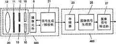
首先,对本发明的第1实施方式进行说明。图3是表示本发明的第1实施方式的摄像装置的整体构成的框图。本实施方式的摄像装置是数字式电子照相机,具有摄像部300和根据从摄像部300发送的信号生成表示图像的信号(图像信号)的信号处理部400。并且,摄像装置既可以只生成静止图像,也可以具有生成动态图像的功能。First, a first embodiment of the present invention will be described. 3 is a block diagram showing the overall configuration of the imaging device according to the first embodiment of the present invention. The imaging device of this embodiment is a digital electronic camera, and includes an
摄像部300具有:光学系统20,其用于成像被摄体;固体摄像元件8(图像传感器),其通过光电转换将光信息转换成电信号;和信号生成/接收部21,其生成用于驱动摄像元件8的基本信号,并接收来自摄像元件8的输出信号,然后发送给信号处理部400。光学系统20具有:光学透镜12、半透明反射镜11、2个反射镜10和2个光学滤光器16。光学透镜12是众所周知的透镜,且可以是具有多个透镜的透镜单元。光学滤光器16是使得用于降低由于像素排列的原因而产生的莫尔图案的水晶低通滤光器与用于除去红外线的红外滤光器组合为一体的滤光器。摄像元件8是典型的CMOS或CCD,且通过众所周知的半导体制造技术制造。摄像元件8与未图示的包括驱动电路或信号处理电路的处理部电连接。信号生成/接收部13以及元件驱动部14由例如CCD驱动器等的LSI构成。The
信号处理部400具有:图像信号生成部25,其处理从摄像部300发送的信号,从而生成图像信号;存储器23,其保存在图像信号的生成过程所产生的各种数据;和图像信号输出部27,其将生成的图像信号发送到外部。图像信号生成部25可通过将众所周知的数字信号处理器(DSP)等的硬件和执行包括图像信号生成处理的图像处理的软件进行组合而很好地实现。存储器23由DRAM等构成。存储器23记录从摄像部300发送的信号,并将通过图像信号生成部25生成的图像数据或被压缩的图像数据进行暂时记录。这些图像数据通过图像信号输出部27被发送到图中未图示的记录介质或显示部等中。The
并且,本实施方式的摄像装置可具有电子快门、取景器、电源(电池)和闪光灯等的众所周知的构成要素,但是,由于并不特别需要这些构成要素的说明以用于理解本发明,因此省略。另外,以上的构成也仅是一个例子,在本发明中,对于除了摄像元件8以及图像信号生成部25以外的构成要素,能适当地组合众所周知的要素来使用。Furthermore, the imaging device of this embodiment may have well-known components such as an electronic shutter, a viewfinder, a power source (battery), and a flash. . In addition, the above configuration is only an example, and in the present invention, components other than the
以下,对本实施方式的光学系统20的构成进行说明。Hereinafter, the configuration of the
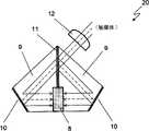
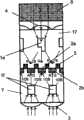
图4是示意性地表示本实施方式的光学系统20的构成的图。光学系统20包括:将从被摄体入射的光聚光的透镜12;和将透过透镜12的光分离成透射光和反射光的半透明反射镜11;和将通过半透明反射镜11分离的两种光分别反射的两个反射镜10。并且,虽然光学系统20可以包括上述光学滤光器16等的其他要素,但是在图4中省略了透镜12、半透明反射镜11和反射镜10以外的构成要素的记载。光学系统20的各构成要素的构成方式为,通过两个反射镜10反射的光分别在摄像元件8中从两侧开始成像。在此,摄像元件8具有支撑半导体层的透明基板,能从设置了布线层的面(表面)以及没有设置布线层的面(背面)两侧接收光。光学系统20以及摄像元件8被容纳并保存在透明封装件9中。透明封装件9是通过将两个透明容器连接而形成的。并且,在图4中,虽然为了方便而将透镜12描述为单一的透镜,但是透镜12一般上可以由在光轴方向排列的多个透镜构成。另外,光学系统20不局限于图4所示的构成,只要在摄像元件8中从两侧开始成像,就可以以任意的方式构成。FIG. 4 is a diagram schematically showing the configuration of an
接下来,对本实施方式的摄像元件8进行说明。Next, the
本实施方式的摄像元件8具有包括表面和背面的半导体层。在表面和背面之间配置有包括以二维状排列的多个光敏单元(像素)的光敏单元阵列。利用两个反射镜10反射的光通过表面或背面入射到光敏单元阵列。各光敏单元是典型的光电二极管,通过光电转换将与入射光量对应的光电转换信号(像素信号)输出。The
图5A是表示本实施方式的像素排列的例子的俯视图。光敏单元阵列200包括例如图5A所示的在摄像面上以正方形晶格状排列的多个光敏单元2。光敏单元阵列200由多个单元块40构成,各单元块40包括4个光敏单元2a、2b、2c和2d。并且,光敏单元的排列可以不是这种正方形晶格状的排列,而既可以是如图5B所示的斜交型的排列,也可以是其他的排列。另外,虽然包含在各单元块中的4个光敏单元2a~2d优选如图5A和5B所示彼此贴近,但是,即使他们相互隔开,也能通过对后面要提到的分光要素阵列采取适当的构成而获得颜色信息。另外,各单元块也可以包含5个以上的光敏单元。FIG. 5A is a plan view showing an example of a pixel arrangement in this embodiment. The
在本实施方式中,在表面侧以及背面侧分别配置与光敏单元阵列200相对置且包括多个分光要素的分光要素阵列。以下,对本实施方式的分光要素进行说明。In this embodiment, light-splitting element arrays facing the
本实施方式的分光要素是利用在折射率不同的两种透光性部件的边界生成的光的衍射,根据波段使入射光朝向不同方向的光学元件。这种类型的分光要素具有用折射率相对高的材料形成的高折射率透明部件(芯部)和用折射率相对低的材料形成并且与芯部的各个侧面相接的低折射率透明部件(包层部)。由于在芯部和包层部之间存在折射率差,因此在透过两者的光之间产生相位差,因此发生衍射。由于该相位差根据光的波长的不同而不同,因此,可根据波段(颜色分量)将光进行空间性分离。例如,可使第1颜色分量的光朝向第1方向,使第1颜色分量以外的光朝向第2方向。另外,能将第1颜色分量的光的一半朝向第1方向,将另一半朝向第2方向,将第1颜色分量以外的光朝向第3方向。而且,还能将彼此不同颜色分量的光朝向3个方向。由于能利用芯部和包层部的折射率差进行分光,因此,在本说明书中,有时将高折射率透明部件称为“分光要素”。关于这种衍射型的分光要素的详细内容,例如日本专利第4264465号公报中进行了公开。The spectroscopic element of this embodiment is an optical element that directs incident light in different directions according to wavelength bands by utilizing diffraction of light generated at the boundary between two types of translucent members having different refractive indices. This type of light-splitting element has a high-refractive-index transparent member (core) formed with a relatively high-refractive-index material and a low-refractive-index transparent member (core) formed with a relatively low-refractive material and in contact with each side of the core. cladding). Since there is a difference in refractive index between the core and the cladding, a phase difference occurs between light passing through both, and thus diffraction occurs. Since this phase difference differs depending on the wavelength of light, it is possible to spatially separate light according to wavelength bands (color components). For example, light of the first color component may be directed in the first direction, and light other than the first color component may be directed in the second direction. Also, half of the light of the first color component can be directed in the first direction, the other half can be directed in the second direction, and light other than the first color component can be directed in the third direction. Furthermore, it is also possible to direct the lights of mutually different color components in three directions. Since light can be split using the difference in refractive index between the core and the clad, in this specification, a high-refractive-index transparent member may be referred to as a "light-splitting element". The details of such diffraction-type spectroscopic elements are disclosed in, for example, Japanese Patent No. 4264465.
具有以上的分光要素的分光要素阵列可以利用众所周知的半导体制造技术,通过执行薄膜的沉积以及构图来制造。通过对分光要素的材质(折射率)、形状、尺寸和排列模式等进行适当地设计,能在各自的光敏单元中将所希望的波段的光进行分离/合并后入射。其结果是,根据各光敏单元所输出的光电转换信号组,能计算出相当于所需的颜色分量的信号。A spectroscopic element array having the above spectroscopic elements can be manufactured by performing thin film deposition and patterning using well-known semiconductor manufacturing techniques. By appropriately designing the material (refractive index), shape, size, arrangement pattern, etc. of the spectroscopic elements, light in a desired wavelength band can be separated/combined and incident on each photosensitive cell. As a result, signals corresponding to desired color components can be calculated from the photoelectric conversion signal group output from each photosensitive cell.
以下,参照图6A~6C对本实施方式的摄像元件10的基本结构以及分光要素的作用进行说明。Hereinafter, the basic configuration of the
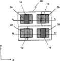
图6A是从表面侧看摄像元件10的基本结构的情况下的俯视图。在本实施方式中,将2行2列的像素构成作为信号处理的基本单位。在表面侧分别配置与光敏单元2a、2d各自相对置的分光要素1a、1d。另外,在背面侧分别配置与光敏单元2b、2c各自相对置的分光要素1b、1c。具有这种基本结构的多个图案重复地形成于摄像元件8的摄像面上。并且,在以下的说明中,使用图中所示的xy坐标,将x轴方向称为“水平方向”,将y轴方向称为“垂直方向”。FIG. 6A is a plan view of the basic structure of the
图6B、6C是分别表示图6A中的AA’线截面以及BB’线截面的图。摄像元件8具有:由硅等的材料构成的半导体层7;配置在半导体层7的内部的光敏单元2a~2d;由在半导体层7的表面侧形成的布线层5以及低折射率透明部件构成的透明层17;和由配置在透明层17的内部的高折射率透明部件构成的分光要素1a、1d以及配置在半导体层7的内部的分光要素1b、1c。在此,分光要素1a、1d具有彼此相同的特性。另外,在分光要素1a、1d中分别聚光的微透镜4隔着透明层17配置在半导体层7的表面侧。同样,在分光要素1b、1c中分别聚光的微透镜3配置在半导体层7的背面层。在半导体层7的表面侧形成了支撑半导体层7或布线层5等的透明基板6。透明基板6隔着透明层17与半导体层7接合。6B and 6C are diagrams respectively showing a section along the line AA' and a section along the line BB' in FIG. 6A . The
图6B、6C所示的结构是通过众所周知的半导体工序制造的。例如,可使用以下的方法制造。首先,在具有一定程度的厚度的半导体基板的表面内部形成光敏单元阵列以及分光要素1b、1c,在表面上形成布线层5、分光要素1a、1d以及微透镜4等构造物。接下来,隔着透明层17将半导体基板和透明基板6接合。然后,通过进行研磨或蚀刻将半导体基板从背面侧开始打薄,例如达到厚度为数微米的程度,形成半导体层7。在形成半导体层7之后,在背面侧形成微透镜3等。在此,背面侧的分光要素1b、1c以及微透镜3配合表面侧的构造物的配置而形成,以便当光从两个面入射时形成在光敏单元阵列上的2个图像重叠。The structures shown in FIGS. 6B and 6C are fabricated by well-known semiconductor processes. For example, it can manufacture using the following method. First, a photosensitive cell array and light-
如图6B所示的分光要素1a、1b由折射率比透明层17以及半导体层7还高的透明材料形成,在光出射一侧的顶端具有梯级。由于透明层17或半导体层7的折射率之差的缘故,将入射光分成0次、1次和-1次等的衍射光。由于它们的衍射角根据波长的不同而不同,因此,能根据颜色分量将光分成2个方向。分光要素1a将绿色光(G)入射到其正下方(相对置)的光敏单元2a,将包含在品红色光的波段中的光(R+B)入射到相邻的光敏单元2b。分光要素1b将包含在黄色光的波段中的光(R+G)入射到其正下方(相对置)的光敏单元2b,将蓝色光(B)入射到相邻的光敏单元2a。微透镜3、4是将水平方向的2像素份和垂直方向的1像素份的光聚光的微透镜,它们在水平方向上彼此相隔1像素间距而配置。The
如图6C所示的分光要素1c、1d也由折射率比透明层17以及半导体层7还高的透明材料形成,在光出射一侧的顶端具有梯级。在表面侧配置的与光敏单元2d相对置的分光要素1d与分光要素1a相比,在水平方向上错开1个像素份配置。在背面侧配置的与光敏单元2c相对置的分光要素1c将包含在青绿色光的波段中的光(G+B)入射到其正下方(相对置)的光敏单元2c,将红光(R)入射到相邻的光敏单元2d。分光要素1d与分光要素1a同样,将绿色光(G)入射到相对置的光敏单元2d,将包含在品红色光的波段中的光(R+B)入射到相邻的光敏单元2c。另外,与分光要素2c的配置相对应地在背面侧配置了微透镜3,与分光要素2d的配置相对应地在表面侧配置了微透镜4。The
如上所述,本实施方式的分光要素并不是都配置在摄像元件的摄像面的一侧,而是分开配置在摄像元件的两侧。通过利用这种分散配置进行颜色分离,能将分光要素的配置密度降低为采用现有技术的情况下的大约1/2。其结果是,能期待彩色摄像元件制造中的构图等的性能的提高。As described above, the spectroscopic elements of this embodiment are not all arranged on one side of the imaging surface of the imaging element, but are separately arranged on both sides of the imaging element. By performing color separation using such a dispersed arrangement, the arrangement density of the spectroscopic elements can be reduced to about 1/2 of the conventional technique. As a result, improvements in performance such as composition in the manufacture of color imaging devices can be expected.
根据以上的构成,通过光学系统20被分成2份的光入射到摄像元件8的表面侧和背面侧的摄像面上。由于透明基板6通过光,因此,摄像元件8中的各光敏单元2a~2d接收从表面侧以及背面侧入射的光。虽然入射到摄像面的一侧的光量由于半透明反射镜的原因而减半,但是,由于微透镜的尺寸相当于2个像素份的尺寸,因此,向各分光要素1a~1d入射相当于在没有设置半透明反射镜的情况下的对1个像素入射的光量的量的光。以下,对各光敏单元的光接收量进行说明。According to the above configuration, the light divided into two by the
首先,对光敏单元2a、2b所接收的光进行说明。从摄像元件8的表面侧入射的光通过透明基板6和微透镜4,被分光要素1a分光为绿色光(G)和绿色光以外(R+B)的光,这些光分别入射到光敏单元2a和2b。另一方面,从摄像元件8的背面侧入射的光通过微透镜3,被分光要素1b分光成蓝色光(B)和蓝色光以外的光(R+G),这些光分别入射到光敏单元2a和2b。First, light received by the
接下来,对光敏单元2c、2d所接收的光进行说明。从摄像元件8的表面侧入射的光通过透明基板6和微透镜4,被分光要素1d分光为绿色光以外的光(R+B)和绿色光(G),这些光分别入射到光敏单元2c和2d。另一方面,从摄像元件8的背面侧入射的光通过微透镜3,被分光要素1c分光成红色光以外的光(G+B)和红色光(R),这些光分别入射到光敏单元2c和2d。Next, the light received by the
通过以上的构成,从光敏单元2a~2d输出的光电转换信号S2a、S2b、S2c和S2d分别用以下的公式6~9表示,其中,将相当于入射光(可见光)、红光、绿光和蓝光的强度的信号分别表示为Ws、Rs、Gs和Bs。With the above configuration, the photoelectric conversion signals S2a, S2b, S2c and S2d output from the
(公式6)S2a=Ws-Rs=Gs+Bs(Formula 6) S2a=Ws-Rs=Gs+Bs
(公式7)S2b=Ws+Rs=2Rs+Gs+Bs(Formula 7) S2b=Ws+Rs=2Rs+Gs+Bs
(公式8)S2c=Ws+Bs=Rs+Gs+2Bs(Formula 8) S2c=Ws+Bs=Rs+Gs+2Bs
(公式9)S2d=Ws-Bs=Rs+Gs(Formula 9) S2d=Ws-Bs=Rs+Gs
根据公式6~9进行加减运算可获得以下的公式10~13。The following formulas 10-13 can be obtained by performing addition and subtraction operations according to formulas 6-9.
(公式10)S2b-S2a=2Rs(Formula 10) S2b-S2a=2Rs
(公式11)S2a+S2b=2Rs+2Gs+2Bs=2Ws(Formula 11) S2a+S2b=2Rs+2Gs+2Bs=2Ws
(公式12)S2c-S2d=2Bs(Formula 12) S2c-S2d=2Bs
(公式13)S2c+S2d=2Rs+2Gs+2Bs=2Ws(Formula 13) S2c+S2d=2Rs+2Gs+2Bs=2Ws
图像信号生成部25(图3)通过使用以公式6~9表示的光电转换信号并执行用公式10~13表示的运算从而生成颜色信息。这样,可通过水平方向(x方向)的光敏单元之间的信号的减法运算来获得R信号以及B信号,可通过水平方向的光敏单元的信号的加法运算来获得W信号。并且,通过从W信号中减去R信号以及B信号可获得G信号。通过以上的信号运算可获得由RGB信号组成的彩色信号。The image signal generating section 25 ( FIG. 3 ) generates color information by using the photoelectric conversion signals expressed in
图像信号生成部15通过针对光敏单元阵列200的每个单元块40分别执行以上的信号运算,生成表示R、G、B的各颜色分量的图像的信号(称为“彩色图像信号”)。所生成的彩色图像信号通过图像信号输出部16被输出到未图示的记录介质或显示部中。The image signal generation unit 15 performs the above signal calculation for each
如上所述,根据本实施方式的摄像装置,能通过使用从4个光敏单元输出的光电转换信号的简单运算进行颜色分离。另一方面,关于像素的分辨率,由于在垂直方向(y方向)上对1个像素以1个单位配置微透镜,因此,不会产生分辨率变差的问题。但是,由于在水平方向(x方向)上对2个像素以1个单位配置微透镜,因此会出现分辨率变差的问题。但是,在本实施方式中,由于微透镜的水平方向的配置是采用每一行错开1个像素份的像素错开的方式,因此,即使是水平方向,也能确保与在对1个像素以1个单位配置微透镜的情况相同程度的分辨率。As described above, according to the imaging device of the present embodiment, color separation can be performed by a simple calculation using the photoelectric conversion signals output from the four photosensitive cells. On the other hand, regarding the resolution of pixels, since the microlenses are arranged in units of one pixel in the vertical direction (y direction), there is no problem of deterioration in resolution. However, since the microlenses are arranged in units of two pixels in the horizontal direction (x direction), there is a problem that the resolution deteriorates. However, in this embodiment, since the arrangement of the microlenses in the horizontal direction adopts the method of staggering the pixels by 1 pixel per row, even in the horizontal direction, it is possible to ensure the same level as that of 1 pixel for 1 pixel. The same degree of resolution as the case where the unit is configured with a microlens.
如上所述,根据本实施方式的摄像装置,由于使用无光吸收的分光要素,因此,能进行光利用率高、灵敏度高的摄像。另外,能使用分光成绿色光(G)和绿色光以外的光(R+B)的分光要素1a以及分光成蓝色光(B)和蓝色光以外的光(R+G)的分光要素1b的组合。同样,能使用分光成红色光(R)和红色光以外的光(G+B)的分光要素1c以及分光成绿色光(G)和绿色光以外的光(R+B)的分光要素1d的组合。根据这种分光要素的组合,能以高灵敏度进行颜色分离,并能获得分辨率也没有问题的图像。而且,由于分光要素在水平方向和垂直方向上都以隔1个像素的方式分散配置在摄像元件8的表面侧和背面侧,因此,每个面的分光要素的配置密度都比现有技术的情况减少,其结果是,具有能提高摄像元件8的制造中的分光要素的构图特性。As described above, according to the imaging device of this embodiment, since the spectroscopic element without light absorption is used, it is possible to perform imaging with high light utilization efficiency and high sensitivity. In addition, the light-splitting
并且,图像信号生成部15可以不用生成所有的三种颜色分量的图像信号。也可以根据用途只生成一种颜色或两种颜色的图像信号。另外,根据需要可以进行信号的放大、合成和修改。Furthermore, the image signal generator 15 does not need to generate image signals of all three color components. It is also possible to generate image signals of only one color or two colors according to the application. In addition, signals can be amplified, synthesized and modified as needed.
另外,虽然理想的是各分光要素严格地具有上述分光性能,但是这些分光性能也可以多少有些偏差。即,从各光敏单元输出的光电转换信号也可以与公式6~9表示的信号多少有些不同。即使各分光要素的分光性能与理想的性能相比有些偏差,也能通过根据偏差的程度对信号进行校正而获得良好的颜色信息。In addition, although it is desirable that each spectroscopic element strictly has the above spectroscopic performance, these spectroscopic properties may vary somewhat. That is, the photoelectric conversion signal output from each photosensitive unit may be somewhat different from the signal represented by formulas 6-9. Even if the spectral performance of each spectroscopic element deviates from the ideal performance, good color information can be obtained by correcting the signal according to the degree of deviation.
而且,本实施方式中的图像信号生成部15进行的信号运算也可以不在摄像装置本身而在其他的设备中执行。例如,通过在接收到从摄像元件8输出的光电转换信号的输入的外部设备中执行规定本实施方式的信号运算处理的程序也能生成颜色信息。In addition, the signal calculation performed by the image signal generation unit 15 in this embodiment may be performed by other equipment instead of the imaging device itself. For example, color information can also be generated by executing a program defining the signal arithmetic processing of the present embodiment in an external device that receives an input of a photoelectric conversion signal output from the
另外,光学系统中的半透明反射镜11不局限于将光2等分的透镜,透射率和反射率也可以不同。在这种情况下,能通过根据透射光和反射光的强度的比率对运算公式进行适当修正来生成颜色信息。In addition, the
在以上的说明中,虽然将分光要素1a~1d设为分别与光敏单元2a~2d相对置,但并不一定需要相对置。各分光要素也可以以覆盖2个光敏单元的方式配置。另外,上述说明的分光要素1a~1d虽然利用衍射将光根据颜色分量进行分离,但也可以采用其他的手段进行分光。例如,作为分光要素1a~1d,也可以使用众所周知的微棱镜或分色镜(dichroic mirror)。In the above description, although the light-
并且,通过各分光要素进行的分光的模式不局限于上述例子。如果是使用将光分光成原色的波段的光(原色光)和其补色的波段的光(补色光)的多个分光要素,各光敏单元能接收两种原色光或两种补色光的构成以及构造,则能通过与上述相同的处理进行颜色分离。Furthermore, the pattern of light splitting by each light splitting element is not limited to the above example. If it is to use a plurality of light-splitting elements that split the light into the light of the primary color band (primary color light) and the light of its complementary color (complementary color light), each photosensitive unit can receive the composition of two primary color lights or two complementary color lights and structure, color separation can be performed by the same process as above.
以下,对将本实施方式的颜色分离处理进行了一般化的情况下的颜色分离处理进行说明。在以下的说明中,入射光(可见光)W被分类成三种原色光Ci、Cj和Ck,它们的补色光分别为(Cj+Ck)、(Ci+Ck)和(Ci+Cj)。另外,将相当于原色光Ci、Cj和Ck的强度的信号分别设为Cis、Cjs和Cks。Hereinafter, the color separation processing in the case of generalizing the color separation processing of the present embodiment will be described. In the following description, incident light (visible light) W is classified into three primary color lights Ci, Cj and Ck, and their complementary color lights are (Cj+Ck), (Ci+Ck) and (Ci+Cj), respectively. In addition, signals corresponding to the intensities of the primary color lights Ci, Cj, and Ck are referred to as Cis, Cjs, and Cks, respectively.
在像这样进行了一般化的情况下,各构成要素可以设置成光敏单元2a从表面侧接收Cj光,且从背面侧接收Ck光。在这种情况下,光敏单元2b从表面侧接收(Ci+Ck)光,且从背面侧接收(Ci+Cj)光。另外,光敏单元2c从表面侧接收(Ci+Ck)光,且从背面侧接收(Cj+Ck)光。光敏单元2d从表面侧接收Cj光,且从背面侧接收Ci光。When generalized in this way, each component can be arranged so that the
根据以上的构成,各光敏单元2a~2d的信号S2a~S2d分别用以下的公式14~17表示。According to the above configuration, the signals S2a to S2d of the respective
(公式14)S2a=Cjs+Cks(Formula 14) S2a=Cjs+Cks
(公式15)S2b=2Cis+Cjs+Cks(Formula 15) S2b=2Cis+Cjs+Cks
(公式16)S2c=Cis+Cjs+2Cks(Formula 16) S2c=Cis+Cjs+2Cks
(公式17)S2d=Cis+Cjs(Formula 17) S2d=Cis+Cjs
通过公式14~17的加减法运算可获得以下的公式18~21。The following formulas 18-21 can be obtained through addition and subtraction of formulas 14-17.
(公式18)S2b-S2a=2Cis(Formula 18) S2b-S2a=2Cis
(公式19)S2a+S2b=2Cis+2Cjs+2Cks=2Ws(Formula 19) S2a+S2b=2Cis+2Cjs+2Cks=2Ws
(公式20)S2c-S2d=2Cks(Formula 20) S2c-S2d=2Cks
(公式21)S2c+S2d=2Cis+2Cjs+2Cks=2Ws(Formula 21) S2c+S2d=2Cis+2Cjs+2Cks=2Ws
即,通过对水平方向的光敏单元之间的信号进行减法运算可获得表示Ci光和Ck光的强度的信号Cis和Cks,通过对水平方向的光敏单元的信号进行加法运算可获得表示W光的强度的信号Ws(=Cis+Cjs+Cks)。通过从获得的Ws中减去Cis以及Cks可获得表示Cj光的强度的信号Cjs。其结果是,可获得三种颜色的彩色信号。从以上的结果可知,如果是1个光敏单元能接收两种原色光以及两种补色光的构成以及构造,则能通过与本实施方式的信号运算处理相同的处理进行颜色分离。That is, the signals Cis and Cks representing the intensity of Ci light and Ck light can be obtained by subtracting the signals between the photosensitive units in the horizontal direction, and the signals Cis and Cks representing the intensity of W light can be obtained by adding the signals of the photosensitive units in the horizontal direction. The intensity of the signal Ws (=Cis+Cjs+Cks). A signal Cjs representing the intensity of Cj light can be obtained by subtracting Cis and Cks from the obtained Ws. As a result, color signals of three colors can be obtained. From the above results, it can be seen that color separation can be performed by the same processing as the signal calculation processing of the present embodiment if one photosensitive cell is configured to receive light of two primary colors and light of two complementary colors.
(实施方式2)(Embodiment 2)
接下来,参照图7A~7C对本发明的第2实施方式进行说明。本实施方式的摄像装置与实施方式1的摄像装置相比,各分光要素的特性不同,其他的构成要素相同。因此,在以下的说明中,以与实施方式1的摄像装置的不同点为中心进行说明,省略重复的说明。Next, a second embodiment of the present invention will be described with reference to FIGS. 7A to 7C . The imaging device of this embodiment is different from the imaging device of
图7A是从表面侧看本实施方式的摄像元件8的像素构成的图。在本实施方式中也以2行2列的像素构成作为信号处理的基本单位。在表面侧分别配置了与光敏单元2a和2d相对置的分光要素1e和1f。另外,在背面侧分别配置了与光敏单元2b和2c相对置的分光要素1g和1h。在此,分光要素1e和分光要素1g具有相同的特性。并且,在图7A中省略了分光要素1e~1h的记载。FIG. 7A is a view showing the pixel configuration of the
图7B是图7A的CC’线剖视图。分光要素1e、1f由折射率比透明层17以及半导体层7还高的透明材料形成,由于透明层17或半导体层7的折射率之差的缘故,将入射光分离成0次、1次和-1次等的衍射光。由于它们的衍射角根据波长的不同而不同,因此,能根据颜色分量将光分成3个方向。在此,分光要素1e在光出射一侧的顶端具有梯级。另一方面,分光要素1f在顶端没有梯级,是正方体形状。分光要素1e将绿色光(G)入射到其正下方(相对置)的光敏单元2a,将红色光(R)入射到相邻的一个光敏单元2b,将蓝色光(B)入射到相邻的另一个光敏单元。在此,相邻的另一个光敏单元属于相邻的单元块(第1相邻单元块),分光要素1f将包含在黄色光的波段中的光(R+G)入射到其正下方(相对置)的光敏单元2b,将蓝色光(B)的各一半入射到光敏单元2a以及包含在相邻的其他单元块(第2相邻单元块)中的光敏单元。并且,分光要素以外的构成要素与实施方式1相同,微透镜3和4的配置关系、尺寸也与实施方式1相同。Fig. 7B is a sectional view taken along line CC' of Fig. 7A. The light-
图7C是图7A的DD’线剖视图。分光要素1g、1h也与分光要素1e、1f相同,由透明的高折射率的材料形成,且利用衍射根据颜色分量将光分离成3个方向。配置在表面侧的与光敏单元2d相对置的分光要素1g与分光要素1e具有相同的特性,并且以相对于分光要素1e在水平方向上错开1个像素份的方式配置。分光要素1h配置在背面侧与光敏单元2c相对置的位置。分光要素1g将绿色光(G)入射到相对置的光敏单元2d,将蓝色光(B)入射到光敏单元2c,将红色光(R)入射到包含在第2相邻单元块中的光敏单元。分光要素1h将包含在青绿色光的波段中的光(G+B)入射到相对置的光敏单元2c,将红色光(R)的各一半分别入射到光敏单元2d以及包含在第1相邻单元块中的光敏单元。并且,根据分光要素1g和1h的配置,微透镜3和4分别以相对置的方式配置。Fig. 7C is a sectional view taken along line DD' in Fig. 7A. The light-
如上所述,在本实施方式中,分光要素也不是都配置在摄像元件的摄像面的单侧,而是分开配置在摄像元件的两侧。通过以这种分散配置的方式进行颜色分离,能将分光要素的配置密度缩小为采用现有技术的情况下的大约1/2。其结果是,可期待在彩色摄像元件的制造中提高构图案等的性能。As described above, in this embodiment, the spectroscopic elements are not all arranged on one side of the imaging surface of the imaging element, but are separately arranged on both sides of the imaging element. By performing color separation in such a dispersed arrangement, the arrangement density of the spectroscopic elements can be reduced to about 1/2 of that in the prior art. As a result, it can be expected to improve the performance of patterning and the like in the manufacture of color imaging devices.
根据以上构成,被摄像光学系统20分成2份的光与实施方式1的情况相同,入射到摄像元件8的表面侧和背面侧的摄像面上。虽然入射到摄像面的一侧的光量通过半透明反射镜而减半,但是,由于微透镜的尺寸相当于2像素份的尺寸,因此,在各分光要素1e~1h中入射相当于对不设置半透明反射镜的情况下的1个像素入射的光量的量的光。以下,对各光敏单元的光接收量进行说明。According to the above configuration, the light divided into two by the imaging
首先,对光敏单元2a、2b接收的光进行说明。光敏单元2a从表面侧接收透过分光要素1e的绿色光(G),从背面侧接收透过2个分光要素1f的蓝色光(B/2+B/2)。在此,2个分光要素1f中的一个与属于第1相邻单元块的1个光敏单元相对置。另一方面,光敏单元2b从表面侧接收透过分光要素1e的红色光(R)和透过与属于第2相邻单元块的1个光敏单元相对置的分光要素的蓝色光(B),从背面侧接收透过用于分光的1f的红色光以及绿色光(R+G)。First, the light received by the
接下来,对光敏单元2c、2d所接收的光进行说明。光敏单元2c从表面侧接收透过分光要素1g的蓝色光(B)和透过与属于第1相邻单元块的1个光敏单元相对置的分光要素1g的红色光(R),从背面侧接收透过分光要素1h的绿色光以及蓝色光(G+B)。光敏单元2d从表面侧接收透过分光要素1g的绿色光(G),从背面侧接收透过2个分光要素1h的红色光(B/2+B/2)。在此,2个分光要素1h中的一个与属于第2相邻单元块的1个光敏单元相对置。Next, the light received by the
根据以上的构成,光敏单元2a~2d的生成信号与实施方式1的生成信号完全相同,分别用公式6~公式9表示。其结果是,与实施方式1相同,能通过4个像素的简单的信号运算进行颜色分离。另外,关于像素的分辨率,由于在垂直方向上对1个像素以1个单位配置微透镜,因此,不会出现分辨率变差的问题。另外,由于在水平方向上对2个像素以1个单位配置微透镜,因此会出现分辨率变差的问题。但是,在本实施方式中,由于微透镜的水平方向的配置是采用每一行错开1个像素份的像素错开的方式,因此,即使是水平方向也能确保与在对1个像素以1个单位配置微透镜的情况相同程度的分辨率。According to the above configuration, the generated signals of the
如上所述,根据本实施方式的摄像装置,由于使用无光吸收的分光要素,因此,可进行光利用率高、灵敏度高的摄像。在本实施方式中,可使用分光成RGB的三种分量的分光要素1e以及分光成蓝色光(B)和蓝色光以外的光(R+G)的分光要素1f的组合。同样,可使用分光成RGB的分光要素1h以及分光成红色光(R)和红色光以外的光(G+B)的分光要素1g的组合。根据这种分光要素的组合,能以高灵敏度进行颜色分离,并能获得分辨率也没有问题的图像。而且,由于分光要素在水平方向和垂直方向上都以隔1个像素的方式分散配置在摄像元件8的表面侧和背面侧,因此,每个面的分光要素的配置密度都比现有技术的情况减少,其结果是,具有能提高摄像元件8的制造中的分光要素的构图特性的效果。As described above, according to the imaging device of this embodiment, since the spectroscopic element without light absorption is used, it is possible to perform imaging with high light utilization efficiency and high sensitivity. In this embodiment, a combination of a light-
在以上的说明中,虽然分光要素1e~1h分别与光敏单元2a~2d相对置设置,但并不一定需要相对置设置。各分光要素也可以以覆盖2个光敏单元的方式配置。另外,上述说明中的分光要素1e~1h虽然利用衍射根据颜色分量将光进行分离,但是也可以通过其他的方法进行分光。例如,作为分光要素1e~1h,也可以使用众所周知的微棱镜或分色镜等。In the above description, although the light-
并且,在本实施方式中,各分光要素的分光模式不局限于上述模式。例如,既可以分别使用实施方式1的分光要素1b、1c来代替分光要素1f、1h,也可以分别使用实施方式1的分光要素1a、1d来代替分光要素1e、1g。如上所述,如果使用分光成RGB的分光要素以及分光成原色和补色的分光要素,则能获得与本实施方式完全相同的效果。在本实施方式中,如果是光敏单元能接收两种原色光或两种补色光的构成以及构造,则也能通过与上述相同的处理进行颜色分离,并能够实现实施方式1所示的一般化。Furthermore, in this embodiment, the spectroscopic pattern of each spectroscopic element is not limited to the above pattern. For example, the
(产业上的可利用性)(industrial availability)
本发明的固体摄像元件以及摄像装置对使用固体摄像元件的所有照相机都有效。例如,可用于数字照相机或数字摄像机等民用照相机或工业用的固体监视照相机等。The solid-state imaging device and imaging device of the present invention are effective for all cameras using a solid-state imaging device. For example, it can be used for consumer cameras such as digital cameras or digital video cameras, or solid-state surveillance cameras for industrial use.
(附图标记的说明)(Explanation of Reference Signs)
1、1a、1b、1c、1d、1e、1f、1g、1h 分光要素1, 1a, 1b, 1c, 1d, 1e, 1f, 1g, 1h Spectral elements
2、2a、2b、2c、2d、摄像元件的光敏单元2, 2a, 2b, 2c, 2d, the photosensitive unit of the imaging element
3、4 微透镜3, 4 microlenses
5 摄像元件的布线层5 The wiring layer of the camera element
6 摄像元件的透明基板6 Transparent substrate of imaging element
7 摄像元件的半导体层7 The semiconductor layer of the imaging element
8 摄像元件8 camera components
9 透明封装件9 transparent packages
10 反射镜10 reflector
11 半透明反射镜11 semi-transparent mirror
12 透镜12 lens
13 反射红色(R)以外的多层膜滤色器13 Multi-layer film color filters other than reflective red (R)
14 只反射绿色(G)的多层膜滤色器14 multi-layer film color filters that only reflect green (G)
15 只反射蓝色(B)的多层膜滤色器15 multi-layer film color filters reflecting blue (B) only
16 光学滤光器16 optical filter
17 透明层17 transparent layer
20 光学系统20 optical system
21 信号生成/接收部21 Signal generation/reception unit
23 存储器23 memory
25 图像信号生成部25 Image Signal Generation Department
27 图像信号输出部27 Image signal output unit
40 单元要素40 unit elements
100 分光要素阵列100 spectroscopic element array
200 光敏单元阵列200 photosensitive cell array
300 摄像部300 Camera Department
400 信号处理部400 Signal Processing Department
Claims (12)
Translated fromChineseApplications Claiming Priority (3)
| Application Number | Priority Date | Filing Date | Title |
|---|---|---|---|
| JP2009-172707 | 2009-07-24 | ||
| JP2009172707 | 2009-07-24 | ||
| PCT/JP2010/004663WO2011010455A1 (en) | 2009-07-24 | 2010-07-21 | Image pickup device and solid-state image pickup element |
Publications (1)
| Publication Number | Publication Date |
|---|---|
| CN102160180Atrue CN102160180A (en) | 2011-08-17 |
Family
ID=43498937
Family Applications (1)
| Application Number | Title | Priority Date | Filing Date |
|---|---|---|---|
| CN2010800026389APendingCN102160180A (en) | 2009-07-24 | 2010-07-21 | Image pickup device and solid-state image pickup element |
Country Status (5)
| Country | Link |
|---|---|
| US (1) | US20110164156A1 (en) |
| JP (1) | JPWO2011010455A1 (en) |
| KR (1) | KR20120039501A (en) |
| CN (1) | CN102160180A (en) |
| WO (1) | WO2011010455A1 (en) |
Cited By (9)
| Publication number | Priority date | Publication date | Assignee | Title |
|---|---|---|---|---|
| CN102510447A (en)* | 2011-09-28 | 2012-06-20 | 上海宏力半导体制造有限公司 | Image sensor |
| CN103477436A (en)* | 2011-12-19 | 2013-12-25 | 松下电器产业株式会社 | Image pickup apparatus |
| CN103503143A (en)* | 2012-05-02 | 2014-01-08 | 松下电器产业株式会社 | Solid-state imaging device |
| CN106847840A (en)* | 2015-09-25 | 2017-06-13 | 三星电子株式会社 | Imageing sensor and the image pick-up device including the imageing sensor |
| CN107017269A (en)* | 2015-10-06 | 2017-08-04 | 三星电子株式会社 | Imaging sensor including recombination dichroic elements |
| CN111614878A (en)* | 2020-05-26 | 2020-09-01 | 维沃移动通信(杭州)有限公司 | Pixel unit, photoelectric sensor, camera module and electronic equipment |
| CN111952325A (en)* | 2014-07-25 | 2020-11-17 | 株式会社半导体能源研究所 | imaging device |
| WO2022134543A1 (en)* | 2020-12-25 | 2022-06-30 | 上海奕瑞光电子科技股份有限公司 | X-ray flat panel detector and photosensitive unit array therefor |
| CN116529637A (en)* | 2020-11-30 | 2023-08-01 | 日本电信电话株式会社 | Optical element, image pickup element, and image pickup device |
Families Citing this family (19)
| Publication number | Priority date | Publication date | Assignee | Title |
|---|---|---|---|---|
| US8208052B2 (en)* | 2008-12-19 | 2012-06-26 | Panasonic Corporation | Image capture device |
| CN101971636B (en)* | 2009-01-14 | 2013-12-04 | 松下电器产业株式会社 | Image capture device |
| JP5331119B2 (en)* | 2009-03-05 | 2013-10-30 | パナソニック株式会社 | Solid-state imaging device and imaging apparatus |
| JP2012015424A (en)* | 2010-07-02 | 2012-01-19 | Panasonic Corp | Solid-state imaging device |
| WO2012174751A1 (en)* | 2011-06-24 | 2012-12-27 | 博立码杰通讯(深圳)有限公司 | Hybrid multi-spectrum photosensitive pixel group, photosensitive device, and photosensitive system |
| JP5975229B2 (en)* | 2011-10-24 | 2016-08-23 | パナソニックIpマネジメント株式会社 | Color imaging device |
| US9071722B2 (en) | 2011-12-26 | 2015-06-30 | Panasonic Intellectual Property Corporation Of America | Solid-state imaging element, imaging device, and signal processing method |
| DE102012221356A1 (en)* | 2012-06-20 | 2013-12-24 | Robert Bosch Gmbh | Sensor and method for detecting light and method and device for determining color information |
| JP6039649B2 (en)* | 2012-09-03 | 2016-12-07 | パナソニック インテレクチュアル プロパティ コーポレーション オブ アメリカPanasonic Intellectual Property Corporation of America | Solid-state imaging device, imaging device, and signal processing method |
| JP2014075780A (en)* | 2012-09-14 | 2014-04-24 | Ricoh Co Ltd | Imaging apparatus and imaging system |
| US9349770B2 (en)* | 2014-02-11 | 2016-05-24 | Semiconductor Components Industries, Llc | Imaging systems with infrared pixels having increased quantum efficiency |
| KR102189675B1 (en) | 2014-04-30 | 2020-12-11 | 삼성전자주식회사 | Image sensor having improved light utilization efficiency |
| KR102159166B1 (en)* | 2014-05-09 | 2020-09-23 | 삼성전자주식회사 | Color separation device and image sensor including the color separation device |
| KR102261855B1 (en)* | 2014-06-13 | 2021-06-07 | 삼성전자주식회사 | Stacked image sensor including color separation element and image pickup apparatus including the stacked image sensor |
| KR102219704B1 (en)* | 2014-06-13 | 2021-02-24 | 삼성전자주식회사 | Color separation element array, image sensor including the color separation element array, and image pickup apparatus including the color separation element array |
| KR102316447B1 (en)* | 2014-08-28 | 2021-10-22 | 삼성전자주식회사 | Image sensor having improved light utilization efficiency |
| KR102313989B1 (en)* | 2014-09-30 | 2021-10-15 | 삼성전자주식회사 | Image sensor and electronic device including the same |
| FR3056333B1 (en)* | 2016-09-22 | 2018-10-19 | Stmicroelectronics (Crolles 2) Sas | ENHANCED QUANTUM EFFICIENT IMAGE SENSOR FOR INFRARED RADIATION |
| WO2021059409A1 (en)* | 2019-09-25 | 2021-04-01 | 日本電信電話株式会社 | Image capture element and image capture device |
Citations (4)
| Publication number | Priority date | Publication date | Assignee | Title |
|---|---|---|---|---|
| JP2000299870A (en)* | 1999-04-13 | 2000-10-24 | Seiko Epson Corp | Digital camera |
| US20050224691A1 (en)* | 2002-05-16 | 2005-10-13 | Koninklijke Philips Electronics N.V. | Image sensor device |
| JP2005333462A (en)* | 2004-05-20 | 2005-12-02 | Canon Inc | Solid-state imaging device and imaging system |
| JP2008072423A (en)* | 2006-09-14 | 2008-03-27 | Fujifilm Corp | Image sensor and digital camera |
Family Cites Families (8)
| Publication number | Priority date | Publication date | Assignee | Title |
|---|---|---|---|---|
| JPS63275168A (en)* | 1987-05-06 | 1988-11-11 | Nec Corp | Solid image pick-up device |
| JP3041276B2 (en)* | 1998-10-26 | 2000-05-15 | 株式会社東芝 | Positioning method of solid-state image sensor |
| JP2001309395A (en)* | 2000-04-21 | 2001-11-02 | Sony Corp | Solid-state imaging device and method of manufacturing the same |
| JP4579384B2 (en)* | 2000-08-09 | 2010-11-10 | キヤノン株式会社 | Color synthesizing optical system and projection display apparatus having the color synthesizing optical system |
| JP4000449B2 (en)* | 2002-02-26 | 2007-10-31 | ソニー株式会社 | Image sensor, imaging device, and mobile phone |
| JP2008172580A (en)* | 2007-01-12 | 2008-07-24 | Toshiba Corp | Solid-state imaging device and solid-state imaging device |
| CN101548381B (en)* | 2007-08-06 | 2011-03-30 | 松下电器产业株式会社 | Optical detection device for imaging |
| US8384818B2 (en)* | 2008-06-18 | 2013-02-26 | Panasonic Corporation | Solid-state imaging device including arrays of optical elements and photosensitive cells |
- 2010
- 2010-07-21CNCN2010800026389Apatent/CN102160180A/enactivePending
- 2010-07-21USUS13/119,317patent/US20110164156A1/ennot_activeAbandoned
- 2010-07-21KRKR1020117006391Apatent/KR20120039501A/ennot_activeWithdrawn
- 2010-07-21WOPCT/JP2010/004663patent/WO2011010455A1/enactiveApplication Filing
- 2010-07-21JPJP2010546991Apatent/JPWO2011010455A1/enactivePending
Patent Citations (4)
| Publication number | Priority date | Publication date | Assignee | Title |
|---|---|---|---|---|
| JP2000299870A (en)* | 1999-04-13 | 2000-10-24 | Seiko Epson Corp | Digital camera |
| US20050224691A1 (en)* | 2002-05-16 | 2005-10-13 | Koninklijke Philips Electronics N.V. | Image sensor device |
| JP2005333462A (en)* | 2004-05-20 | 2005-12-02 | Canon Inc | Solid-state imaging device and imaging system |
| JP2008072423A (en)* | 2006-09-14 | 2008-03-27 | Fujifilm Corp | Image sensor and digital camera |
Cited By (17)
| Publication number | Priority date | Publication date | Assignee | Title |
|---|---|---|---|---|
| CN102510447B (en)* | 2011-09-28 | 2016-08-10 | 上海华虹宏力半导体制造有限公司 | Imageing sensor |
| CN102510447A (en)* | 2011-09-28 | 2012-06-20 | 上海宏力半导体制造有限公司 | Image sensor |
| CN103477436A (en)* | 2011-12-19 | 2013-12-25 | 松下电器产业株式会社 | Image pickup apparatus |
| US9496300B2 (en) | 2011-12-19 | 2016-11-15 | Panasonic Intellectual Property Management Co., Ltd. | Imaging device having array of spectroscopic sections wherein an interval between two spectroscopic sections at a periphery of an imaging plane is smaller than an interval between two spectroscopic sections at a center of the imaging plane |
| CN103477436B (en)* | 2011-12-19 | 2017-05-17 | 松下知识产权经营株式会社 | camera device |
| CN103503143A (en)* | 2012-05-02 | 2014-01-08 | 松下电器产业株式会社 | Solid-state imaging device |
| CN103503143B (en)* | 2012-05-02 | 2016-12-28 | 松下电器(美国)知识产权公司 | Solid-state imager and camera head |
| CN111952325A (en)* | 2014-07-25 | 2020-11-17 | 株式会社半导体能源研究所 | imaging device |
| CN106847840A (en)* | 2015-09-25 | 2017-06-13 | 三星电子株式会社 | Imageing sensor and the image pick-up device including the imageing sensor |
| CN106847840B (en)* | 2015-09-25 | 2021-12-31 | 三星电子株式会社 | Image sensor and image pickup device including the same |
| CN107017269A (en)* | 2015-10-06 | 2017-08-04 | 三星电子株式会社 | Imaging sensor including recombination dichroic elements |
| CN107017269B (en)* | 2015-10-06 | 2022-01-18 | 三星电子株式会社 | Image sensor including color separation element |
| CN111614878A (en)* | 2020-05-26 | 2020-09-01 | 维沃移动通信(杭州)有限公司 | Pixel unit, photoelectric sensor, camera module and electronic equipment |
| CN111614878B (en)* | 2020-05-26 | 2022-04-22 | 维沃移动通信(杭州)有限公司 | Pixel unit, photoelectric sensor, camera module and electronic equipment |
| US12063424B2 (en) | 2020-05-26 | 2024-08-13 | Vivo Mobile Communication Co., Ltd. | Pixel unit, photoelectric sensor, camera module and electronic device |
| CN116529637A (en)* | 2020-11-30 | 2023-08-01 | 日本电信电话株式会社 | Optical element, image pickup element, and image pickup device |
| WO2022134543A1 (en)* | 2020-12-25 | 2022-06-30 | 上海奕瑞光电子科技股份有限公司 | X-ray flat panel detector and photosensitive unit array therefor |
Also Published As
| Publication number | Publication date |
|---|---|
| KR20120039501A (en) | 2012-04-25 |
| WO2011010455A1 (en) | 2011-01-27 |
| US20110164156A1 (en) | 2011-07-07 |
| JPWO2011010455A1 (en) | 2012-12-27 |
Similar Documents
| Publication | Publication Date | Title |
|---|---|---|
| CN102160180A (en) | Image pickup device and solid-state image pickup element | |
| CN102714738B (en) | Solid-state imaging element and imaging device | |
| JP5331107B2 (en) | Imaging device | |
| CN102484723B (en) | Solid-state imaging element, imaging device, and signal processing method | |
| CN102577395B (en) | Solid-state image pickup element and image pickup apparatus | |
| CN103503143B (en) | Solid-state imager and camera head | |
| CN101779288A (en) | solid state imaging device | |
| CN103907189B (en) | Solid-state imager, camera head and signal processing method | |
| CN102959961B (en) | Solid-state imager, camera head and signal processing method | |
| CN103222267B (en) | Solid-state imaging element, imaging device, and signal processing method | |
| JP5997149B2 (en) | Solid-state imaging device, imaging apparatus, and signal processing method | |
| CN103503144B (en) | Solid-state imaging device | |
| JPWO2010100896A1 (en) | Imaging device and double-sided irradiation type solid-state imaging device | |
| JP2014086743A (en) | Solid-state image sensor, imaging apparatus and signal processing method | |
| JP2014086742A (en) | Solid-state image sensor, imaging apparatus and signal processing method |
Legal Events
| Date | Code | Title | Description |
|---|---|---|---|
| C06 | Publication | ||
| PB01 | Publication | ||
| C10 | Entry into substantive examination | ||
| SE01 | Entry into force of request for substantive examination | ||
| C02 | Deemed withdrawal of patent application after publication (patent law 2001) | ||
| WD01 | Invention patent application deemed withdrawn after publication | Application publication date:20110817 |