CN102160103B - Display device - Google Patents
Display deviceDownload PDFInfo
- Publication number
- CN102160103B CN102160103BCN2009801371896ACN200980137189ACN102160103BCN 102160103 BCN102160103 BCN 102160103BCN 2009801371896 ACN2009801371896 ACN 2009801371896ACN 200980137189 ACN200980137189 ACN 200980137189ACN 102160103 BCN102160103 BCN 102160103B
- Authority
- CN
- China
- Prior art keywords
- oxide semiconductor
- semiconductor layer
- layer
- transistor
- wiring
- Prior art date
- Legal status (The legal status is an assumption and is not a legal conclusion. Google has not performed a legal analysis and makes no representation as to the accuracy of the status listed.)
- Active
Links
Images


Classifications
- H—ELECTRICITY
- H10—SEMICONDUCTOR DEVICES; ELECTRIC SOLID-STATE DEVICES NOT OTHERWISE PROVIDED FOR
- H10D—INORGANIC ELECTRIC SEMICONDUCTOR DEVICES
- H10D86/00—Integrated devices formed in or on insulating or conducting substrates, e.g. formed in silicon-on-insulator [SOI] substrates or on stainless steel or glass substrates
- H10D86/40—Integrated devices formed in or on insulating or conducting substrates, e.g. formed in silicon-on-insulator [SOI] substrates or on stainless steel or glass substrates characterised by multiple TFTs
- G—PHYSICS
- G02—OPTICS
- G02F—OPTICAL DEVICES OR ARRANGEMENTS FOR THE CONTROL OF LIGHT BY MODIFICATION OF THE OPTICAL PROPERTIES OF THE MEDIA OF THE ELEMENTS INVOLVED THEREIN; NON-LINEAR OPTICS; FREQUENCY-CHANGING OF LIGHT; OPTICAL LOGIC ELEMENTS; OPTICAL ANALOGUE/DIGITAL CONVERTERS
- G02F1/00—Devices or arrangements for the control of the intensity, colour, phase, polarisation or direction of light arriving from an independent light source, e.g. switching, gating or modulating; Non-linear optics
- G02F1/01—Devices or arrangements for the control of the intensity, colour, phase, polarisation or direction of light arriving from an independent light source, e.g. switching, gating or modulating; Non-linear optics for the control of the intensity, phase, polarisation or colour
- G02F1/13—Devices or arrangements for the control of the intensity, colour, phase, polarisation or direction of light arriving from an independent light source, e.g. switching, gating or modulating; Non-linear optics for the control of the intensity, phase, polarisation or colour based on liquid crystals, e.g. single liquid crystal display cells
- G02F1/133—Constructional arrangements; Operation of liquid crystal cells; Circuit arrangements
- G02F1/136—Liquid crystal cells structurally associated with a semi-conducting layer or substrate, e.g. cells forming part of an integrated circuit
- G02F1/1362—Active matrix addressed cells
- G02F1/136204—Arrangements to prevent high voltage or static electricity failures
- G—PHYSICS
- G02—OPTICS
- G02F—OPTICAL DEVICES OR ARRANGEMENTS FOR THE CONTROL OF LIGHT BY MODIFICATION OF THE OPTICAL PROPERTIES OF THE MEDIA OF THE ELEMENTS INVOLVED THEREIN; NON-LINEAR OPTICS; FREQUENCY-CHANGING OF LIGHT; OPTICAL LOGIC ELEMENTS; OPTICAL ANALOGUE/DIGITAL CONVERTERS
- G02F1/00—Devices or arrangements for the control of the intensity, colour, phase, polarisation or direction of light arriving from an independent light source, e.g. switching, gating or modulating; Non-linear optics
- G02F1/01—Devices or arrangements for the control of the intensity, colour, phase, polarisation or direction of light arriving from an independent light source, e.g. switching, gating or modulating; Non-linear optics for the control of the intensity, phase, polarisation or colour
- G02F1/13—Devices or arrangements for the control of the intensity, colour, phase, polarisation or direction of light arriving from an independent light source, e.g. switching, gating or modulating; Non-linear optics for the control of the intensity, phase, polarisation or colour based on liquid crystals, e.g. single liquid crystal display cells
- G02F1/133—Constructional arrangements; Operation of liquid crystal cells; Circuit arrangements
- G02F1/136—Liquid crystal cells structurally associated with a semi-conducting layer or substrate, e.g. cells forming part of an integrated circuit
- G02F1/1362—Active matrix addressed cells
- G02F1/136286—Wiring, e.g. gate line, drain line
- H—ELECTRICITY
- H10—SEMICONDUCTOR DEVICES; ELECTRIC SOLID-STATE DEVICES NOT OTHERWISE PROVIDED FOR
- H10D—INORGANIC ELECTRIC SEMICONDUCTOR DEVICES
- H10D30/00—Field-effect transistors [FET]
- H10D30/60—Insulated-gate field-effect transistors [IGFET]
- H10D30/67—Thin-film transistors [TFT]
- H10D30/674—Thin-film transistors [TFT] characterised by the active materials
- H10D30/6755—Oxide semiconductors, e.g. zinc oxide, copper aluminium oxide or cadmium stannate
- H—ELECTRICITY
- H10—SEMICONDUCTOR DEVICES; ELECTRIC SOLID-STATE DEVICES NOT OTHERWISE PROVIDED FOR
- H10D—INORGANIC ELECTRIC SEMICONDUCTOR DEVICES
- H10D86/00—Integrated devices formed in or on insulating or conducting substrates, e.g. formed in silicon-on-insulator [SOI] substrates or on stainless steel or glass substrates
- H10D86/40—Integrated devices formed in or on insulating or conducting substrates, e.g. formed in silicon-on-insulator [SOI] substrates or on stainless steel or glass substrates characterised by multiple TFTs
- H10D86/421—Integrated devices formed in or on insulating or conducting substrates, e.g. formed in silicon-on-insulator [SOI] substrates or on stainless steel or glass substrates characterised by multiple TFTs having a particular composition, shape or crystalline structure of the active layer
- H10D86/423—Integrated devices formed in or on insulating or conducting substrates, e.g. formed in silicon-on-insulator [SOI] substrates or on stainless steel or glass substrates characterised by multiple TFTs having a particular composition, shape or crystalline structure of the active layer comprising semiconductor materials not belonging to the Group IV, e.g. InGaZnO
- H—ELECTRICITY
- H10—SEMICONDUCTOR DEVICES; ELECTRIC SOLID-STATE DEVICES NOT OTHERWISE PROVIDED FOR
- H10D—INORGANIC ELECTRIC SEMICONDUCTOR DEVICES
- H10D86/00—Integrated devices formed in or on insulating or conducting substrates, e.g. formed in silicon-on-insulator [SOI] substrates or on stainless steel or glass substrates
- H10D86/40—Integrated devices formed in or on insulating or conducting substrates, e.g. formed in silicon-on-insulator [SOI] substrates or on stainless steel or glass substrates characterised by multiple TFTs
- H10D86/441—Interconnections, e.g. scanning lines
- H—ELECTRICITY
- H10—SEMICONDUCTOR DEVICES; ELECTRIC SOLID-STATE DEVICES NOT OTHERWISE PROVIDED FOR
- H10D—INORGANIC ELECTRIC SEMICONDUCTOR DEVICES
- H10D86/00—Integrated devices formed in or on insulating or conducting substrates, e.g. formed in silicon-on-insulator [SOI] substrates or on stainless steel or glass substrates
- H10D86/40—Integrated devices formed in or on insulating or conducting substrates, e.g. formed in silicon-on-insulator [SOI] substrates or on stainless steel or glass substrates characterised by multiple TFTs
- H10D86/60—Integrated devices formed in or on insulating or conducting substrates, e.g. formed in silicon-on-insulator [SOI] substrates or on stainless steel or glass substrates characterised by multiple TFTs wherein the TFTs are in active matrices
- H—ELECTRICITY
- H10—SEMICONDUCTOR DEVICES; ELECTRIC SOLID-STATE DEVICES NOT OTHERWISE PROVIDED FOR
- H10D—INORGANIC ELECTRIC SEMICONDUCTOR DEVICES
- H10D89/00—Aspects of integrated devices not covered by groups H10D84/00 - H10D88/00
- H10D89/60—Integrated devices comprising arrangements for electrical or thermal protection, e.g. protection circuits against electrostatic discharge [ESD]
- H10D89/601—Integrated devices comprising arrangements for electrical or thermal protection, e.g. protection circuits against electrostatic discharge [ESD] for devices having insulated gate electrodes, e.g. for IGFETs or IGBTs
- H10D89/811—Integrated devices comprising arrangements for electrical or thermal protection, e.g. protection circuits against electrostatic discharge [ESD] for devices having insulated gate electrodes, e.g. for IGFETs or IGBTs using FETs as protective elements
- H—ELECTRICITY
- H10—SEMICONDUCTOR DEVICES; ELECTRIC SOLID-STATE DEVICES NOT OTHERWISE PROVIDED FOR
- H10K—ORGANIC ELECTRIC SOLID-STATE DEVICES
- H10K59/00—Integrated devices, or assemblies of multiple devices, comprising at least one organic light-emitting element covered by group H10K50/00
- H10K59/10—OLED displays
- H10K59/12—Active-matrix OLED [AMOLED] displays
- H10K59/121—Active-matrix OLED [AMOLED] displays characterised by the geometry or disposition of pixel elements
- H10K59/1213—Active-matrix OLED [AMOLED] displays characterised by the geometry or disposition of pixel elements the pixel elements being TFTs
- H—ELECTRICITY
- H10—SEMICONDUCTOR DEVICES; ELECTRIC SOLID-STATE DEVICES NOT OTHERWISE PROVIDED FOR
- H10K—ORGANIC ELECTRIC SOLID-STATE DEVICES
- H10K59/00—Integrated devices, or assemblies of multiple devices, comprising at least one organic light-emitting element covered by group H10K50/00
- H10K59/10—OLED displays
- H10K59/12—Active-matrix OLED [AMOLED] displays
- H10K59/131—Interconnections, e.g. wiring lines or terminals
Landscapes
- Physics & Mathematics (AREA)
- Nonlinear Science (AREA)
- Engineering & Computer Science (AREA)
- Microelectronics & Electronic Packaging (AREA)
- Mathematical Physics (AREA)
- Chemical & Material Sciences (AREA)
- Crystallography & Structural Chemistry (AREA)
- General Physics & Mathematics (AREA)
- Optics & Photonics (AREA)
- Geometry (AREA)
- Thin Film Transistor (AREA)
- Liquid Crystal (AREA)
- Devices For Indicating Variable Information By Combining Individual Elements (AREA)
- Semiconductor Integrated Circuits (AREA)
- Metal-Oxide And Bipolar Metal-Oxide Semiconductor Integrated Circuits (AREA)
- Electroluminescent Light Sources (AREA)
- Electrodes Of Semiconductors (AREA)
- Shift Register Type Memory (AREA)
- Electrochromic Elements, Electrophoresis, Or Variable Reflection Or Absorption Elements (AREA)
- Noodles (AREA)
- Mechanical Treatment Of Semiconductor (AREA)
- Bipolar Transistors (AREA)
Abstract
Description
Translated fromChinese技术领域technical field
本发明涉及一种包括氧化物半导体的显示装置。The present invention relates to a display device including an oxide semiconductor.
背景技术Background technique
以液晶显示装置为代表的形成在诸如玻璃衬底的平板上的薄膜晶体管使用非晶硅、或多晶硅制造。使用非晶硅的薄膜晶体管具有如下特性:虽然其场效应迁移率低,但是这种晶体管适合于在玻璃衬底上大面积地形成。另一方面,使用结晶硅制造的薄膜晶体管具有如下特性:虽然其场效应迁移率高,但是需要进行激光退火等的结晶化工序,因此其不一定适合于较大玻璃衬底。A thin film transistor formed on a flat plate such as a glass substrate typified by a liquid crystal display device is manufactured using amorphous silicon, or polycrystalline silicon. A thin film transistor using amorphous silicon has characteristics that, although its field-effect mobility is low, such a transistor is suitable for being formed over a large area on a glass substrate. On the other hand, thin film transistors manufactured using crystalline silicon have characteristics that although they have high field-effect mobility, they require a crystallization process such as laser annealing, so they are not necessarily suitable for larger glass substrates.
另一方面,使用氧化物半导体制造薄膜晶体管,并将其应用于电子装置或光学装置的技术受到注目。例如,专利文献1及专利文献2公开作为氧化物半导体膜使用氧化锌(ZnO)、In-Ga-Zn-O类氧化物半导体来制造薄膜晶体管,并将这种晶体管用作图像显示装置的开关元件等的技术。On the other hand, technologies for manufacturing thin film transistors using oxide semiconductors and applying them to electronic devices or optical devices are attracting attention. For example,
[专利文献1]日本专利申请公开2007-123861号公报[Patent Document 1] Japanese Patent Application Publication No. 2007-123861
[专利文献2]日本专利申请公开2007-96055号公报[Patent Document 2] Japanese Patent Application Publication No. 2007-96055
发明内容Contents of the invention
将氧化物半导体用作沟道形成区域的薄膜晶体管具有如下特性:其工作速度比使用非晶硅的薄膜晶体管快,并且其制造工序比使用多晶硅的薄膜晶体管简单。换言之,通过使用氧化物半导体,即使在300℃以下的低温下也可以制造场效应迁移率高的薄膜晶体管。A thin film transistor using an oxide semiconductor as a channel formation region has characteristics that its operating speed is faster than that of a thin film transistor using amorphous silicon, and its manufacturing process is simpler than that of a thin film transistor using polysilicon. In other words, by using an oxide semiconductor, a thin film transistor with high field-effect mobility can be manufactured even at a low temperature of 300° C. or lower.
为了有效地利用工作特性优良并可在低温下制造的包括氧化物半导体的显示装置的特征,包括适当的结构的保护电路是必要的。此外,重要的是,保证包括氧化物半导体的显示装置的可靠性。In order to effectively utilize the characteristics of a display device including an oxide semiconductor which is excellent in operating characteristics and can be manufactured at a low temperature, a protection circuit including an appropriate structure is necessary. Furthermore, it is important to ensure the reliability of a display device including an oxide semiconductor.
本发明的一实施例的目的在于提供适合于保护电路的结构。An object of an embodiment of the present invention is to provide a structure suitable for protecting circuits.
本发明的一实施例的目的在于:在通过层叠除氧化物半导体以外的绝缘膜及导电膜来制造的各种用途的显示装置中,增强保护电路的功能并使工作稳定化。An object of an embodiment of the present invention is to enhance the function of a protection circuit and stabilize operation in a display device for various applications manufactured by laminating an insulating film and a conductive film other than an oxide semiconductor.
本发明的一实施例是一种显示装置,其中保护电路使用包括氧化物半导体的非线性元件形成。该非线性元件包括氧含量不同的氧化物半导体的组合。An embodiment of the present invention is a display device in which a protection circuit is formed using a nonlinear element including an oxide semiconductor. The nonlinear element includes a combination of oxide semiconductors with different oxygen contents.
本发明的示例性实施例是一种显示装置,包括:在具有绝缘表面的衬底上彼此交叉地设置的扫描线和信号线,像素电极排列为矩阵的像素部;以及在该像素部的外部区域中使用氧化物半导体形成的非线性元件。像素部包括将沟道形成区域形成于第一氧化物半导体层中的薄膜晶体管。像素部中的薄膜晶体管包括:连接至扫描线的栅电极;连接至信号线并与第一氧化物半导体层接触的第一布线层;以及连接至像素电极并与第一氧化物半导体层接触的第二布线层。此外,在像素部和置于衬底周边部的信号输入端子之间设置有非线性元件。非线性元件包括:栅电极;覆盖该栅电极的栅极绝缘层;在栅极绝缘层上重叠于栅电极的第一氧化物半导体层;以及其端部在第一氧化物半导体层上与栅电极重叠,且其中层叠有导电层和第二氧化物半导体层的一对第一布线层及第二布线层。非线性元件的栅电极连接至扫描线或信号线连接,且非线性元件的第一布线层或第二布线层通过第三布线层连接至栅电极,从而向第一布线层或第二布线层施加栅电极电位。An exemplary embodiment of the present invention is a display device including: a scan line and a signal line arranged to cross each other on a substrate having an insulating surface, a pixel portion in which pixel electrodes are arranged in a matrix; and A nonlinear element formed using an oxide semiconductor in the region. The pixel portion includes a thin film transistor in which a channel formation region is formed in the first oxide semiconductor layer. The thin film transistor in the pixel portion includes: a gate electrode connected to the scan line; a first wiring layer connected to the signal line and in contact with the first oxide semiconductor layer; and a gate electrode connected to the pixel electrode and in contact with the first oxide semiconductor layer. second wiring layer. In addition, a non-linear element is provided between the pixel portion and the signal input terminal disposed at the peripheral portion of the substrate. The nonlinear element includes: a gate electrode; a gate insulating layer covering the gate electrode; a first oxide semiconductor layer overlapping the gate electrode on the gate insulating layer; The electrodes are overlapped, and a pair of first wiring layer and second wiring layer of a conductive layer and a second oxide semiconductor layer are stacked therein. The gate electrode of the nonlinear element is connected to the scanning line or the signal line, and the first wiring layer or the second wiring layer of the nonlinear element is connected to the gate electrode through the third wiring layer, thereby providing the first wiring layer or the second wiring layer A gate electrode potential is applied.
本发明的一示例性实施例是一种显示装置,包括:在具有绝缘表面的衬底上彼此交叉地设置的扫描线与信号线,像素电极排列为矩阵的像素部;以及该像素部的外部区域中的保护电路。像素部包括将沟道形成区域形成于第一氧化物半导体层的薄膜晶体管。像素部中的薄膜晶体管包括:连接至扫描线的栅电极;连接至信号线并与第一氧化物半导体层接触的第一布线层;以及连接至像素电极并与第一氧化物半导体层接触的第二布线层。在像素部的外部区域中设置有用于使扫描线与公共布线相互连接的保护电路、以及使信号线和公共布线相互连接的保护电路。保护电路包括非线性元件,该非线性元件包括:栅电极;覆盖该栅电极的栅极绝缘层;在栅极绝缘层上与栅电极重叠的第一氧化物半导体层;以及其端部在第一氧化物半导体层上与栅电极重叠,且其中层叠有导电层和第二氧化物半导体层的一对第一布线层及第二布线层。此外,非线性元件的第一布线层或第二布线层通过第三布线层连接至栅电极。An exemplary embodiment of the present invention is a display device including: scanning lines and signal lines arranged to cross each other on a substrate having an insulating surface, a pixel portion in which pixel electrodes are arranged in a matrix; and an outer portion of the pixel portion protection circuit in the area. The pixel portion includes a thin film transistor in which a channel formation region is formed in the first oxide semiconductor layer. The thin film transistor in the pixel portion includes: a gate electrode connected to the scan line; a first wiring layer connected to the signal line and in contact with the first oxide semiconductor layer; and a gate electrode connected to the pixel electrode and in contact with the first oxide semiconductor layer. second wiring layer. A protection circuit for interconnecting the scanning line and the common wiring, and a protection circuit for interconnecting the signal line and the common wiring are provided in an outer region of the pixel portion. The protection circuit includes a nonlinear element including: a gate electrode; a gate insulating layer covering the gate electrode; a first oxide semiconductor layer overlapping the gate electrode on the gate insulating layer; A pair of first wiring layer and second wiring layer of a conductive layer and a second oxide semiconductor layer are stacked on the first oxide semiconductor layer overlapping with the gate electrode. In addition, the first wiring layer or the second wiring layer of the nonlinear element is connected to the gate electrode through the third wiring layer.
在此,第一氧化物半导体层的氧浓度高于第二氧化物半导体层的氧浓度。换言之,第一氧化物半导体层是氧过量型,并且第二氧化物半导体层是氧缺乏型。第一氧化物半导体层的导电率低于第二氧化物半导体层的导电率。第一氧化物半导体层及第二氧化物半导体层具有非单晶结构,并包含至少一种非晶成分。另外,第二氧化物半导体层有时在非晶结构中包含纳米晶体。Here, the oxygen concentration of the first oxide semiconductor layer is higher than the oxygen concentration of the second oxide semiconductor layer. In other words, the first oxide semiconductor layer is an oxygen-excess type, and the second oxide semiconductor layer is an oxygen-deficient type. The conductivity of the first oxide semiconductor layer is lower than that of the second oxide semiconductor layer. The first oxide semiconductor layer and the second oxide semiconductor layer have a non-single crystal structure and include at least one amorphous component. In addition, the second oxide semiconductor layer sometimes contains nanocrystals in an amorphous structure.
注意,为方便起见在该说明书中使用诸如“第一”、“第二”等序数词,但其并不表示步骤顺序或层叠顺序。另外,本说明书中的序数词不表示指定本发明的特定名称。Note that ordinal numerals such as "first" and "second" are used in this specification for convenience, but they do not indicate the order of steps or the order of layers. In addition, the ordinal number in this specification does not represent the specific name which designates this invention.
根据本发明的一实施例,通过使用包括氧化物半导体的非线性元件形成保护电路,可得到具有适合于保护电路的结构的显示装置。在非线性元件的第一氧化物半导体层与布线层之间的连接结构中,设置接合于其导电率高于第一氧化物半导体层的导电率的第二氧化物半导体层的区域,这与只采用金属布线的情况相比,可进行稳定工作。由此,可增强保护电路的功能并实现工作的稳定化。According to an embodiment of the present invention, by forming a protection circuit using a nonlinear element including an oxide semiconductor, a display device having a structure suitable for the protection circuit can be obtained. In the connection structure between the first oxide semiconductor layer and the wiring layer of the nonlinear element, a region bonded to the second oxide semiconductor layer whose conductivity is higher than that of the first oxide semiconductor layer is provided, which is the same as Compared with the case of using only metal wiring, stable operation can be performed. Thus, the function of the protection circuit can be enhanced and the operation can be stabilized.
附图说明Description of drawings
在附图中:In the attached picture:
图1示出显示装置中的包括信号输入端子、扫描线、信号线、以及非线性元件的保护电路和像素部之间的位置关系;1 shows a positional relationship between a protection circuit including a signal input terminal, a scanning line, a signal line, and a non-linear element and a pixel portion in a display device;
图2示出保护电路的一示例;Figure 2 shows an example of a protection circuit;
图3示出保护电路的一示例;Figure 3 shows an example of a protection circuit;
图4A和4B是示出保护电路的一示例的平面图;4A and 4B are plan views showing an example of a protection circuit;
图5A和5B是示出保护电路的一示例的截面图;5A and 5B are cross-sectional views illustrating an example of a protection circuit;
图6A和6B是示出保护电路的一示例的平面图;6A and 6B are plan views showing an example of a protection circuit;
图7A和7B是示出保护电路的一示例的平面图;7A and 7B are plan views showing an example of a protection circuit;
图8A至8C是示出保护电路的制造工序的截面图;8A to 8C are cross-sectional views showing the manufacturing process of the protection circuit;
图9A至9C是示出保护电路的制造工序的截面图;9A to 9C are cross-sectional views showing the manufacturing process of the protection circuit;
图10是电子纸的截面图;10 is a cross-sectional view of electronic paper;
图11A和11B各自是半导体装置的框图;11A and 11B are each a block diagram of a semiconductor device;
图12示出信号线驱动器电路的结构;Fig. 12 shows the structure of the signal line driver circuit;
图13示出信号线驱动器电路操作的时序图;FIG. 13 shows a timing diagram of the operation of the signal line driver circuit;
图14示出信号线驱动器电路操作的时序图;FIG. 14 shows a timing diagram of the operation of the signal line driver circuit;
图15是示出移位寄存器结构的框图;Fig. 15 is a block diagram showing the structure of a shift register;
图16示出图14所示的触发器连接结构;Fig. 16 shows the flip-flop connection structure shown in Fig. 14;
图17A-1、17A-2及17B是示出实施例6的半导体装置的俯视图及截面图;17A-1, 17A-2 and 17B are a plan view and a cross-sectional view showing a semiconductor device of Embodiment 6;
图18是示出实施例6的半导体装置的截面图;18 is a cross-sectional view showing a semiconductor device of Embodiment 6;
图19示出实施例7的半导体装置的像素等效电路;FIG. 19 shows a pixel equivalent circuit of the semiconductor device of Embodiment 7;
图20A至20C各示出实施例7的半导体装置;20A to 20C each show a semiconductor device of Embodiment 7;
图21A及21B是描述实施例7的半导体装置的俯视图及截面图;21A and 21B are a plan view and a cross-sectional view illustrating a semiconductor device of Embodiment 7;
图22A和22B示出电子纸的应用示例;22A and 22B illustrate an application example of electronic paper;
图23是示出电子书籍装置的一示例的外观图;FIG. 23 is an external view showing an example of an electronic book device;
图24A是电视机示例的外观图,图24B是数码相框示例的外观图;Fig. 24A is an appearance diagram of an example of a television set, and Fig. 24B is an appearance diagram of an example of a digital photo frame;
图25A和25B是示出游戏机示例的外观图;25A and 25B are external views showing examples of gaming machines;
图26是示出移动电话机示例的外观图;Fig. 26 is an external view showing an example of a mobile phone;
图27是示出保护电路示例的截面图。Fig. 27 is a cross-sectional view showing an example of a protection circuit.
具体实施方式Detailed ways
下面,参照附图对本发明的实施例进行描述。本发明不限于以下描述,所属技术领域的普通技术人员可以很容易地理解一个事实就是,其方式及细节可按各种各样的形式改变而不背离本发明的范围及精神。因此,本发明不应该被解释为仅限于以下实施例的描述。在以下说明的本发明的结构中,所有附图中使用相同的附图标记来表示相同的部分。Hereinafter, embodiments of the present invention will be described with reference to the accompanying drawings. The present invention is not limited to the following description, and those skilled in the art can easily understand the fact that the modes and details thereof can be changed in various forms without departing from the scope and spirit of the present invention. Therefore, the present invention should not be construed as being limited to the description of the following embodiments. In the configuration of the present invention described below, the same reference numerals are used throughout the drawings to denote the same parts.
实施例1Example 1
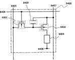
在实施例1中,参照附图说明包括像素部和包括设置在像素部周边的非线性元件的保护电路的显示装置的一示例。In
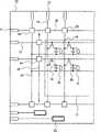
图1示出显示装置中的包括信号输入端子、扫描线、信号线、以及非线性元件的保护电路及像素部之间的位置关系。在具有绝缘表面的衬底10上扫描线13与信号线14彼此交叉以构成像素部17。FIG. 1 shows the positional relationship between a protection circuit including a signal input terminal, a scanning line, a signal line, and a nonlinear element, and a pixel portion in a display device. Scanning
像素部17包括排列为矩阵的多个像素18。像素18包括连接到扫描线13和信号线14的像素晶体管19、存储电容器部20、像素电极21。The
在本文中示出的像素结构中,存储电容器部20的一电极连接至像素晶体管19,而另一电极连接至电容器线22。此外,像素电极21形成驱动显示元件(诸如液晶元件、发光元件、对比度介质(电子墨))的一电极。这些显示元件的另一电极连接到公共端子23。In the pixel structure shown here, one electrode of the
保护电路设置在像素部17以及端子11和端子12之间。在实施例1中,设置多个保护电路。因此,即使归因于静电等的浪涌电压施加到扫描线13、信号线14及电容器总线27,像素晶体管19等不被破坏。相应地,保护电路具有当向该保护电路施加浪涌电压时,向公共布线29或公共布线28释放电荷的结构。The protection circuit is provided between the
在实施例1中,在扫描线13一侧设置保护电路24,在信号线14一侧设置保护电路25,在电容器总线27上设置保护电路26。不言而喻,保护电路的结构不限于此。In
图2示出保护电路的一示例。该保护电路包括相对于扫描线13并联安排的非线性元件30及非线性元件31。非线性元件30及非线性元件31各自包括诸如二极管的二端子元件或诸如晶体管等的三端子元件。例如,可与像素部的像素晶体管相同的步骤形成非线性元件。例如通过连接非线性元件的栅极端子和漏极端子,可实现与二极管类似的特性。FIG. 2 shows an example of a protection circuit. The protection circuit includes a
非线性元件30的第一端子(栅极)和第三端子(漏极)连接到扫描线13,而其第二端子(源极)连接到公共布线29。非线性元件31的第一端子(栅极)和第三端子(漏极)连接到公共布线29,而第二端子(源极)连接到扫描线13。即,图2所示的保护电路包括两个晶体管,该两个晶体管的整流方向彼此相反,且使扫描线13和公共布线29彼此连接。换言之,在扫描线13和公共布线29之间存在其整流方向从扫描线13向公共布线29的晶体管和其整流方向从公共布线29向扫描线13的晶体管。A first terminal (gate) and a third terminal (drain) of the
在图2所示的保护电路中,当相对于公共布线29,扫描线13因静电等而带正电或负电时,电流在消除电荷的方向上流动。例如,当扫描线13带正电时,电流向将其正电荷释放到公共布线29的方向流动。通过该工作,可以防止连接到带电的扫描线13的像素晶体管19的静电击穿或阈值电压的移动。此外,可防止带电的扫描线13与另一布线之间的电介质击穿,该另一布线隔着绝缘层与带点的扫描线13交叉。In the protection circuit shown in FIG. 2 , when the
此外,在图2中,使用将第一端子(栅极)连接到扫描线13的非线性元件30以及将第一端子(栅极)连接到公共布线29的非线性元件31;即,非线性元件30和非线性元件31的整流方向彼此相反。经由各非线性元件的第二端子(源极)和第三端子(漏极)连接公共布线29和扫描线13;换言之,非线性元件30和非线性元件31并联。作为另一结构,还可以进一步添加并联连接的非线性元件,从而增强保护电路的工作稳定性。例如,图3示出设置在扫描线13和公共布线29之间并包括非线性元件30a和非线性元件30b以及非线性元件31a和非线性元件31b的保护电路。该保护电路共包括4个非线性元件:将其各自的第一端子(栅极)连接到公共布线29的两个非线性元件(30b、31b)和将其各自的第一端子(栅极)连接到扫描线13的两个非线性元件(30a、31a)。换言之,在公共布线29和扫描线13之间连接两对非线性元件,各对非线性元件以使其整流方向彼此相反的方式设置。换言之,在扫描线13和公共布线29之间连接其整流方向从扫描线13向公共布线29的两个晶体管和其整流方向从公共布线29向扫描线13的两个晶体管。这样,通过利用四个非线性元件连接公共布线29和扫描线13时,不仅在对扫描线13施加浪涌电压的情况,而且由静电等使公共布线29带电的情况下,可防止其电荷直接流过扫描线13。注意,图6A示出四个非线性元件740a、740b、740c、740d设置在衬底上的示例且6B示出其等效电路图。在此,附图标记650和651分别表示扫描线和公共布线。In addition, in FIG. 2, a
图7A示出在衬底上使用奇数个非线性元件形成保护电路的示例,而图7B示出其等效电路图。在该电路中,将非线性元件730b、非线性元件730a连接到非线性元件730c作为开关元件。像这样,通过串联连接非线性元件,可分散对保护电路的非线性元件施加的瞬时负载。在此,附图标记650和651分别表示扫描线和公共布线。FIG. 7A shows an example of forming a protection circuit using an odd number of nonlinear elements on a substrate, and FIG. 7B shows an equivalent circuit diagram thereof. In this circuit, a
图2示出在扫描线13一侧设置的保护电路,但是可将与其具有类似结构的保护电路设置在信号线14一侧。FIG. 2 shows a protection circuit provided on the
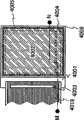
图4A是示出保护电路一示例的平面图,而图4B是其等效电路图。图5A和5B是沿着图4A所示的Q1-Q2线得到的截面图。以下参照图4A和4B以及图5A和5B说明保护电路的一个结构示例。FIG. 4A is a plan view showing an example of a protection circuit, and FIG. 4B is an equivalent circuit diagram thereof. 5A and 5B are cross-sectional views taken along line Q1-Q2 shown in FIG. 4A. One structural example of the protection circuit is described below with reference to FIGS. 4A and 4B and FIGS. 5A and 5B.
非线性元件170a及非线性元件170b分别包括使用与扫描线13相同的层形成的栅电极101及栅电极16。在栅电极101及栅电极16上形成有栅极绝缘层102。在栅极绝缘层102上形成第一氧化物半导体层103,并且在栅电极101上彼此相对的方式设置第一布线层38及第二布线层39。栅极绝缘层102由氧化硅或氧化铝等的氧化物形成。此外,非线性元件170a及非线性元件170b在主要部分中具有相同结构。The
第一氧化物半导体层103以在彼此相对的第一布线层38及第二布线层39下方隔着栅极绝缘膜覆盖栅电极101的方式设置。换言之,第一氧化物半导体层103与栅电极101重叠,并与栅极绝缘层102的上表面部和第二氧化物半导体层104a及104b的下表面部接触地设置。在此,第一布线层38具有从第一氧化物半导体层103一侧层叠有第二氧化物半导体层104a和导电层105a的结构,并且第二布线层39具有从第一氧化物半导体层103一侧层叠有第二氧化物半导体层104b和导电层105b的结构。The first
第一氧化物半导体层103的氧浓度高于第二氧化物半导体层(104a及104b)的氧浓度。换言之,第一氧化物半导体层103是氧过量型,而第二氧化物半导体层(104a及104b)是氧缺乏型。通过增大第一氧化物半导体层103的氧浓度,可以减少施主型缺陷,而可得到载流子寿命更长和迁移率更高的有利效果。另一方面,使第二氧化物半导体层(104a及104b)的氧浓度低于第一氧化物半导体层103的氧浓度时,可提高载流子浓度且第二氧化物半导体层(104a和104b)可用于形成源区及漏区。The oxygen concentration of the first
关于氧化物半导体的结构,第一氧化物半导体层103是包括In、Ga、Zn及O的非单晶氧化物半导体层,并具有至少一种非晶成分,而第二氧化物半导体层(104a及104b)是包括In、Ga、Zn及O的非单晶氧化物半导体层,且有时在其非单晶结构中包括纳米晶体。则,第一氧化物半导体层103具有的特性为其导电率低于第二氧化物半导体层(104a及104b)的导电率。因此,实施例1的非线性元件170a及非线性元件170b中的第二氧化物半导体层(104a及104b)起到与晶体管的源区及漏区类似的功能。作为源区的第二氧化物半导体层104a及作为漏区的第二氧化物半导体层104b具有n型导电性,且其激活能(ΔE)为0.01eV至0.1eV,并且第二氧化物半导体层(140a和104b)也可称为n+区域。Regarding the structure of the oxide semiconductor, the first
第一氧化物半导体层103及第二氧化物半导体层(104a及104b)典型地由氧化锌(ZnO)形成或由包含In、Ga及Zn的氧化物半导体形成。The first
第二氧化物半导体层(104a及104b)与第一氧化物半导体层103、导电层(105a及105b)接触并在其之间设置,并获得具有不同特性的氧化物半导体层的结。通过在第一氧化物半导体层和导电层之间设置其导电率高于第一氧化物半导体层103的第二氧化物半导体层(104a及104b),这与第一氧化物半导体层和导电层直接接触情况下的肖特基结相比,稳定工作变得可能。换言之,热稳定性提高,从而可实现稳定工作。由此,可提增强护电路功能并实现工作的稳定化。此外,结漏(junction leak)降低,并可提高非线性元件170a及非线性元件170b的特性。The second oxide semiconductor layer (104a and 104b) is in contact with and disposed between the first
在第一氧化物半导体层103上设置有保护绝缘膜107。保护绝缘膜107由氧化硅或氧化铝等的氧化物形成。此外,通过在氧化硅或氧化铝上层叠氮化硅、氮化铝、氧氮化硅或氧氮化铝,可以增强保护膜的功能。A protective
不管是上述哪一种情况,与第一氧化物半导体层103接触的保护绝缘膜107是氧化物,其可防止从第一氧化物半导体层103抽出氧并防止第一氧化物半导体层103变成氧缺乏型。此外,通过采用其中第一氧化物半导体层103不直接接触于包括氮化物的绝缘层的结构,可防止氮化物中的氢扩散并在第一氧化物半导体层103中产生归因于羟基等的缺陷。In either case, the protective
在保护绝缘膜107中设置有接触孔125及128,其中使用与栅电极101相同的层形成的扫描线13连接至非线性元件170a的第三端子(漏极)。使用由与像素部的像素电极相同材料形成的第三布线层110形成该连接。第三布线层110由用于形成透明导电膜的例如,氧化铟锡(ITO:indium tinoxide)、氧化锌(ZnO)、氧化锡(SnO2)的材料形成。由此,第三布线层110比由金属材料形成的布线具有更高电阻。当保护电路包括包含这种电阻成分的布线时,可防止因过大电流流过而损坏非线性元件170a。In the protective
虽然图4A和4B及图5A和5B示出针对扫描线13设置的保护电路的示例,类似保护电路可应用于信号线、电容器总线等。Although FIGS. 4A and 4B and FIGS. 5A and 5B show examples of protection circuits provided for the
根据实施例1,通过以该方式设置包括氧化物半导体的保护电路,可得到具有适合于保护电路的结构的显示装置。由此,可增强保护电路的功能并实现工作的稳定化。According to
实施例2Example 2
在实施例2中,参照图8A至8C以及图9A至9C对形成有实施例1中图4A所示的像素部和像素部周边的包括非线性元件的保护电路的显示装置的制造工序的一实施例进行说明。图8A至8C及图9A至9C是沿着图4A中的Q1-Q2线得到的截面图。In
在图8A中,作为具有透光性的衬底100,可使用在市场上销售的钡硼硅酸盐玻璃、铝硼硅酸盐玻璃、铝硅酸盐玻璃等的玻璃衬底。例如,优选使用以组分比计算氧化钡(BaO)多于硼酸(B2O3),且应变点为730℃或更高的玻璃衬底。这是因为当在700℃左右的高温下对氧化物半导体层进行热处理时,玻璃衬底也不应变的缘故。In FIG. 8A , commercially available glass substrates such as barium borosilicate glass, aluminoborosilicate glass, and aluminosilicate glass can be used as the light-transmitting
接着,在整个衬底100上形成导电层。之后,由第一光刻工序形成抗蚀剂掩模,并且通过蚀刻去除不必要的部分来形成布线及电极(包括栅电极101的栅极布线、电容器布线以及端子)。此时进行蚀刻,以便将栅电极101的至少一端部形成为锥形。Next, a conductive layer is formed on the
包括栅电极101的栅极布线、电容器布线、端子部的端子优选使用诸如铝(Al)或铜(Cu)的低电阻导电材料形成;然而,铝本身具有诸如低耐热性以及易于腐蚀的缺点,所以与耐热导电材料组合来使用。作为耐热导电材料可使用选自钛(Ti)、钽(Ta)、钨(W)、钼(Mo)、铬(Cr)、钕(Nd)、或钪(Sc)中的元素、或包括任何以上元素的合金、包括这种元素组合的合金膜或者包括任何以上元素的氮化物膜。Gate wiring including the
接着,在整个栅电极101上形成栅极绝缘层102。栅极绝缘层102通过利用溅射法等并以50nm至250nm的厚度形成。Next, a
例如,通过溅射法形成100nm厚度的氧化硅膜作为栅极绝缘层102。当然,栅极绝缘层102不限于这种氧化硅膜,且可以是包括另一绝缘膜的单层或者叠层,另一绝缘膜为氧氮化硅膜、氮化硅膜、氧化铝膜、或氧化钽膜等。For example, a silicon oxide film with a thickness of 100 nm is formed as the
接着,在形成第一氧化物半导体层之前对栅极绝缘层102进行等离子体处理。在此,进行其中通过将氧气体和氩气导入沉积腔内以产生等离子体的反溅射,从而对栅极绝缘层进行使用氧自由基或氧的处理。像这样,去除附着在表面的尘埃,并且使栅极绝缘层表面变为氧过量区域。对栅极绝缘层表面进行氧自由基处理,以使表面变为氧过量区域有效,因为在后面的工序中的用于提高可靠性的热处理(200℃至600℃)中,制成用于改善栅极绝缘层和第一氧化物半导体层之间的界面的氧供应源。Next, the
通过溅射法并适当地改变导入腔体内的气体以及腔体内的靶,可在不暴露于大气的情况下连续形成栅极绝缘层、第一氧化物半导体层及第二氧化物半导体层。不暴露于大气并连续成膜可防止杂质的混入。在不暴露于大气并连续成膜的情况下,优选使用多腔型制造装置。The gate insulating layer, the first oxide semiconductor layer, and the second oxide semiconductor layer can be continuously formed without exposure to the atmosphere by sputtering and appropriately changing the gas introduced into the chamber and the target in the chamber. Continuous film formation without exposure to the atmosphere prevents contamination of impurities. In the case of continuous film formation without exposure to the atmosphere, it is preferable to use a multi-chamber manufacturing apparatus.
特别地,优选连续形成与第一氧化物半导体层接触的栅极绝缘层102和第一氧化物半导体层。通过这样的连续成膜,可形成叠层之间的没有被诸如大气中的水分或污染杂质元素或尘埃的大气成分所污染的界面。因此,可减小非线形元件及薄膜晶体管的特性的不均匀。In particular, it is preferable to continuously form the
注意,在本说明书中的术语“连续成膜”意味着:在从利用溅射法进行的第一成膜步骤到利用溅射法进行的第二成膜步骤的一系列步骤中,置有要被处理衬底的气氛不被大气等的污染气氛污染,而一直控制为真空或惰性气体气氛(氮气气氛或稀有气体气氛)。通过进行连续成膜,可避免水分等再附着的情况下,可在已清净化的衬底上进行成膜。Note that the term "continuous film formation" in this specification means: in a series of steps from the first film formation step by the sputtering method to the second film formation step by the sputtering method, the The atmosphere of the substrate to be processed is not polluted by a polluted atmosphere such as the air, but is always controlled as a vacuum or an inert gas atmosphere (nitrogen atmosphere or rare gas atmosphere). By performing continuous film formation, it is possible to form a film on a cleaned substrate while avoiding re-attachment of moisture, etc.
接着,不使进行等离子体处理的衬底暴露于大气地形成第一氧化物半导体层。通过不使进行等离子体处理的衬底暴露于大气地形成第一氧化物半导体层,可避免尘埃和水分附着在栅极绝缘层和半导体膜之间的界面的问题。在此,使用直径8英寸的包含In、Ga及Zn的氧化物半导体靶(组成比是In2O3∶Ga2O3∶ZnO=1∶1∶1),将衬底和靶之间的距离设定为170mm,将压力设定为0.4Pa,将直流(DC)电源设定为0.5kW的条件下,并在氧气氛下形成第一氧化物半导体层。此外,优选使用脉冲直流(DC)电源,因为可减少尘埃,并且膜厚可均匀。将第一氧化物半导体层的厚度设定为5nm至200nm。在实施例2中将第一氧化物半导体层的厚度设定为100nm。Next, the first oxide semiconductor layer is formed without exposing the plasma-treated substrate to the atmosphere. By forming the first oxide semiconductor layer without exposing the substrate subjected to the plasma treatment to the atmosphere, the problem of dust and moisture adhering to the interface between the gate insulating layer and the semiconductor film can be avoided. Here, an oxide semiconductor target containing In, Ga, and Zn (composition ratio: In2 O3 : Ga2 O3 : ZnO = 1:1:1) with a diameter of 8 inches was used, and the gap between the substrate and the target was The first oxide semiconductor layer was formed in an oxygen atmosphere under conditions where the distance was set to 170 mm, the pressure was set to 0.4 Pa, and the direct current (DC) power supply was set to 0.5 kW. In addition, it is preferable to use a pulsed direct current (DC) power supply because dust can be reduced and the film thickness can be made uniform. The thickness of the first oxide semiconductor layer is set to 5 nm to 200 nm. In Example 2, the thickness of the first oxide semiconductor layer was set to 100 nm.
第一氧化物半导体层的成膜条件与第二氧化物半导体层的成膜条件不同时,第一氧化物半导体层具有与第二氧化物半导体层不同的组分;例如,第一氧化物半导体层比第二氧化物半导体层包含更多氧。例如,该情况下,与第二氧化物半导体层的沉积条件中的氧气流速和氩气流速相比,在第一氧化物半导体层的沉积条件中氧气流速增大。具体而言,第二氧化物半导体层在稀有气体(诸如氩或氦)气氛下(或者包含10%或以下的氧气且90%或以上的氩气的气体)形成,而第一氧化物半导体层在氧气气氛下(或者氧气流速等于或大于氩气流速的氧气和氩气的混合气体,并且氧气流速∶氩气流速=1∶1或以上)形成。第一氧化物半导体层比第二氧化物半导体层包含更多氧时,可使第一氧化物半导体层的导电率低于第二氧化物半导体层的导电率。另外,第一氧化物半导体层包含大量氧时,可降低截止电流;因此,可得到导通/截止比高的薄膜晶体管。When the film-forming conditions of the first oxide semiconductor layer are different from those of the second oxide semiconductor layer, the first oxide semiconductor layer has a composition different from that of the second oxide semiconductor layer; for example, the first oxide semiconductor layer layer contains more oxygen than the second oxide semiconductor layer. For example, in this case, the flow rate of oxygen gas is increased in the deposition conditions of the first oxide semiconductor layer compared to the flow rate of oxygen gas and the flow rate of argon in the deposition conditions of the second oxide semiconductor layer. Specifically, the second oxide semiconductor layer is formed under a rare gas (such as argon or helium) atmosphere (or a gas containing 10% or less of oxygen and 90% or more of argon), while the first oxide semiconductor layer Formed under an oxygen atmosphere (or a mixed gas of oxygen and argon with an oxygen flow rate equal to or greater than the argon flow rate, and an oxygen flow rate: argon flow rate = 1:1 or more). When the first oxide semiconductor layer contains more oxygen than the second oxide semiconductor layer, the conductivity of the first oxide semiconductor layer can be made lower than that of the second oxide semiconductor layer. In addition, when the first oxide semiconductor layer contains a large amount of oxygen, off-current can be reduced; therefore, a thin film transistor with a high on/off ratio can be obtained.
第一氧化物半导体层可在与先前进行反溅射的处理腔相同的处理腔中形成,或者只要不暴露于大气的情况下进行成膜,可在与先前进行反溅射的处理腔不同的处理腔中形成。The first oxide semiconductor layer may be formed in the same processing chamber as that in which reverse sputtering was previously performed, or may be formed in a different processing chamber from that in which reverse sputtering was previously performed as long as the film formation is performed without exposure to the atmosphere. formed in the processing chamber.
接着,利用溅射法在第一氧化物半导体层上形成第二氧化物半导体层。在此,使用将氧化铟(In2O3)、氧化镓(Ga2O3)、氧化锌(ZnO)的组分比设定为1∶1∶1(=In2O3∶Ga2O3∶ZnO)的靶,将衬底和靶之间的距离设定为170mm,将沉积腔的压力设定为0.4Pa,将直流(DC)电源设定为0.5kW,将沉积温度设定为室温,并且导入流速40sccm的氩气的条件下,进行溅射沉积。由此,形成以In、Ga、Zn及氧为成分的半导体膜作为第二氧化物半导体层。虽然意图性地使用将其组分比为In2O3∶Ga2O3∶ZnO=1∶1∶1的靶,但是刚成膜后常获得包括1nm至10nm大小晶粒的氧化物半导体膜。此外,通过适当地调节反应性溅射的沉积条件,诸如靶的组分比、沉积压力(0.1Pa至2.0Pa)、电功率(250W至3000W:8英寸φ)、温度(室温至100℃)等,可调节是否有晶粒、晶粒密度,并且将晶粒直径调节在1nm至10nm的范围内。将第二氧化物半导体层的厚度设定为5nm至20nm。当然,当在膜中包含晶粒时,所包含的晶粒大小不超过膜厚。在实施例2中将第二氧化物半导体层的厚度设定为5nm。Next, a second oxide semiconductor layer is formed on the first oxide semiconductor layer by sputtering. Here, the composition ratio of indium oxide (In2 O3 ), gallium oxide (Ga2 O3 ), and zinc oxide (ZnO) was set to 1:1:1 (=In2 O3 :Ga2 O3 : ZnO) target, the distance between the substrate and the target is set to 170mm, the pressure of the deposition chamber is set to 0.4Pa, the direct current (DC) power supply is set to 0.5kW, and the deposition temperature is set to Sputter deposition was performed at room temperature and under the condition of introducing argon gas at a flow rate of 40 sccm. Thus, a semiconductor film containing In, Ga, Zn, and oxygen as components is formed as the second oxide semiconductor layer. Although a target whose composition ratio is In2 O3 :Ga2 O3 : ZnO=1:1:1 is intentionally used, an oxide semiconductor film including crystal grains of 1 nm to 10 nm in size is often obtained immediately after film formation . In addition, by properly adjusting the deposition conditions of reactive sputtering, such as target composition ratio, deposition pressure (0.1Pa to 2.0Pa), electric power (250W to 3000W: 8 inches φ), temperature (room temperature to 100°C), etc. , can adjust whether there are grains, grain density, and adjust the grain diameter in the range of 1nm to 10nm. The thickness of the second oxide semiconductor layer is set to 5 nm to 20 nm. Of course, when grains are included in the film, the grain size included does not exceed the film thickness. In Example 2, the thickness of the second oxide semiconductor layer was set to 5 nm.
接着,进行第二光刻工序以形成抗蚀剂掩模,并且对第一氧化物半导体层及第二氧化物半导体层进行蚀刻。在此,通过使用ITO07N(日本关东化学公司的产品)的湿法蚀刻,以去除不必要的部分;因此形成第一氧化物半导体层103及第二氧化物半导体层111。注意,在此蚀刻不限于湿法蚀刻,也可利用干法蚀刻。图8B示出该阶段中的截面。Next, a second photolithography process is performed to form a resist mask, and the first oxide semiconductor layer and the second oxide semiconductor layer are etched. Here, unnecessary portions are removed by wet etching using ITO07N (product of Kanto Chemical Co., Ltd.); thus, the first
接着,在第二氧化物半导体层111及栅极绝缘层102上利用溅射法或真空蒸镀法由金属材料形成导电膜132。作为导电膜132的材料,有选自Al、Cr、Ta、Ti、Mo、W中的元素、包含以上述元素的合金、以上元素的一些组合的合金膜等。Next, a
在200℃至600℃下进行热处理的情况下,优选使导电膜具有承受该热处理的耐热性。因为铝本身具有诸如耐热性低并易于腐蚀的问题,所以与耐热导电材料组合来使用。作为与Al组合使用的耐热导电材料,可使用选自钛(Ti)、钽(Ta)、钨(W)、钼(Mo)、铬(Cr)、钕(Nd)、钪(Sc)中的元素、包含任何以上元素的合金、包含以上元素的组合的合金膜或者包括任何以上元素的氮化膜。In the case of performing heat treatment at 200° C. to 600° C., it is preferable to impart heat resistance to the conductive film to withstand the heat treatment. Since aluminum itself has problems such as low heat resistance and easy corrosion, it is used in combination with a heat-resistant conductive material. As a heat-resistant conductive material used in combination with Al, one selected from titanium (Ti), tantalum (Ta), tungsten (W), molybdenum (Mo), chromium (Cr), neodymium (Nd), and scandium (Sc) can be used. element, an alloy containing any of the above elements, an alloy film containing a combination of the above elements, or a nitride film containing any of the above elements.
在本实施例中,导电膜132具有如下三层结构:形成Ti膜,在该Ti膜上层叠包含Nd的铝(Al-Nd)膜,并且在其上形成另一Ti膜。替代地,导电膜132可具有两层结构,其中可在铝膜上层叠钛膜。另外,导电膜132可具有包含硅的铝膜或钛膜铝膜单层结构。图8C示出该阶段中的截面。In the present embodiment, the
接着,进行第三光刻工序以形成抗蚀剂掩模131,并且通过蚀刻去除导电膜132的不必要的部分。从而形成导电层105a及105b(参照图9A)。此时,可使用湿法蚀刻或干法蚀刻。在此,采用使用SiCl4、Cl2和BCl3的混合气体的干法蚀刻对层叠Ti膜、包含Nd的铝(Al-Nd)膜和Ti膜的导电膜进行蚀刻。以该方式,形成导电膜105a及105b。Next, a third photolithography process is performed to form a resist
接着,使用与用于蚀刻导电膜132的抗蚀剂掩模相同的抗蚀剂掩模对第二氧化物半导体层进行蚀刻。在此,通过使用ITO07N(日本关东化学公司的产品)的湿法蚀刻去除不必要的部分;从而形成第二氧化物半导体层104a、104b。注意,此时的蚀刻不限于湿法蚀刻而也可以使用干法蚀刻。此外,虽然取决于蚀刻条件,但是在第二氧化物半导体层111的蚀刻工序中,第一氧化物半导体层103的露出区域也受到蚀刻。因此,在第二氧化物半导体层104a、104b之间的第一氧化物半导体层103的沟道形成区域如图9A所示成为膜厚薄的区域。Next, the second oxide semiconductor layer is etched using the same resist mask as that used to etch the
此外,可以对第一氧化物半导体层103进行氧等离子体处理。通过进行该等离子体处理,可修复因对第一氧化物半导体层103进行蚀刻而产生的损伤。在典型的氧等离子体处理中,利用通过氧气辉光放电等离子体产生的自由基对氧化物半导体表面进行处理。但是产生等离子体的气体不限于氧,也可以是氧气和稀有气体的混合气体。In addition, oxygen plasma treatment may be performed on the first
接着,优选进行200℃至600℃,典型地300℃至500℃的热处理。在该情况下,在炉中在氮气氛下进行350℃、一个小时的热处理。该热处理允许包含In、Ga及Zn的半导体层的原子重新排列。由于通过该热处理消除阻挡载流子迁移的歪曲,所以在此进行的热处理(包括光退火)重要。此外,进行热处理的时序只要是第一氧化物半导体层形成后,就没有特别的限制;例如可在形成保护膜后进行热处理。通过以上步骤,可完成以第一氧化物半导体层103为沟道形成区域的非线性元件170a。图9A示出该阶段中的截面图。Next, heat treatment at 200°C to 600°C, typically 300°C to 500°C is preferably performed. In this case, heat treatment was performed at 350° C. for one hour in a furnace under a nitrogen atmosphere. This heat treatment allows atomic rearrangement of the semiconductor layer including In, Ga, and Zn. The heat treatment (including photo annealing) performed here is important because the distortion that blocks carrier transfer is eliminated by this heat treatment. In addition, the timing of performing the heat treatment is not particularly limited as long as it is after the formation of the first oxide semiconductor layer; for example, the heat treatment may be performed after the formation of the protective film. Through the above steps, the
接着,去除抗蚀剂掩模,并且形成覆盖包含In、Ga及Zn的半导体层的保护绝缘膜107。保护绝缘膜107可使用通过溅射法等得到的氮化硅膜、氧化硅膜、氧氮化硅膜、氧化铝膜、氧化钽膜等形成。Next, the resist mask is removed, and a protective
接着,进行第四光刻工序以形成抗蚀剂掩模,并且进行对保护绝缘膜107的蚀刻。从而形成到达导电层105b的接触孔125。为了缩减掩模数,优选使用同一抗蚀剂掩模对栅极绝缘层102进行蚀刻,以便形成到达栅电极的接触孔128。图9B示出该阶段中的截面图。Next, a fourth photolithography process is performed to form a resist mask, and etching of the protective
接着,在去除抗蚀剂掩模之后形成透明导电膜。作为透明导电膜的材料可为氧化铟In2O3)、氧化铟氧化锡合金(In2O3-SnO2,以下简称ITO)等,且它们使用溅射法、真空蒸镀法等形成。通过利用盐酸基溶液进行上述材料的蚀刻处理。但是,因为对ITO的蚀刻尤其容易留下残渣,可使用氧化铟氧化锌合金In2O3-ZnO)以改善蚀刻加工性。Next, a transparent conductive film is formed after removing the resist mask. Materials for the transparent conductive film include indium oxide (In2 O3 ), indium oxide tin oxide alloy (In2 O3 -SnO2 , hereinafter referred to as ITO), and the like, and they are formed using sputtering, vacuum evaporation, or the like. The etching treatment of the above-mentioned materials is performed by using a hydrochloric acid-based solution. However, since etching of ITO is particularly prone to leaving residues, an indium oxide zinc oxide alloy (In2 O3 —ZnO) may be used to improve etching workability.
接着,进行第五光刻工序以形成抗蚀剂掩模,并去除透明导电膜的不必要的部分。从而形成未图示的像素电极。Next, a fifth photolithography process is performed to form a resist mask and remove unnecessary portions of the transparent conductive film. Thus, a not-shown pixel electrode is formed.
另外,在该第五光刻工序中,通过使用栅极绝缘层102及保护绝缘膜107为电介质,由电容器布线和像素电极一起形成电容器部中的存储电容器,未示出。In addition, in this fifth photolithography process, by using the
另外,在该第五光刻工序中,利用抗蚀剂掩模覆盖端子部来保留形成在端子部中的透明导电膜。透明导电膜用作用于与FPC连接的电极或布线、用作源极布线的输入端子的用于连接的端子电极等。In addition, in this fifth photolithography process, the terminal portion is covered with a resist mask to leave the transparent conductive film formed in the terminal portion. The transparent conductive film is used as an electrode or wiring for connection with FPC, a terminal electrode for connection serving as an input terminal of source wiring, and the like.
此外,在实施例2中,经由透明导电膜构成的第三布线层110通过接触孔125及128将非线性元件170a的作为漏电极层的导电层105b连接至扫描线108,并由此形成保护电路。In addition, in
接着,去除抗蚀剂掩模。图9C示出该阶段中的截面图。Next, the resist mask is removed. Figure 9C shows a cross-sectional view at this stage.
通过以上述方式进行的五次光刻工序,可通过使用五个光掩模完成具有多个非线性元件(在实施例2中,具有两个非线性元件170a以及170b)的保护电路。在非线性元件的第一氧化物半导体层和布线层之间的连接结构中,设置接合到其导电率高于第一氧化物半导体层的第二氧化物半导体层的区域,这与仅使用金属布线的情况相比,可进行稳定工作。根据实施例2,可与非线性元件一起并以与非线性元件类似的方法完成多个TFT。因此可同时进行包括底栅n沟道TFT的像素部和保护电路的制造。换言之,根据实施例2所示的步骤,可制造安装有具有较少归因于膜剥离的缺陷的保护二极管的有源矩阵显示装置衬底。Through five photolithography processes performed in the above manner, a protection circuit having a plurality of non-linear elements (in
实施例3Example 3
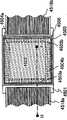
现将参照图27在实施例3中说明包括像素部和像素部周边的包括非线性元件的保护电路的显示装置的与实施例2不同的一实施例。An embodiment different from
图27是在同一衬底上形成有安排在像素部中的薄膜晶体管和包括非线性元件的保护电路的显示装置的截面图。将非线性元件270a中,将作为源电极及漏电极的导电层(105a、105b)设置成与第一氧化物半导体层103接触。27 is a cross-sectional view of a display device in which a thin film transistor arranged in a pixel portion and a protection circuit including a nonlinear element are formed over the same substrate. In the
在非线性元件270a中,优选导电层105a及导电层105b与通过等离子体处理改良的第一氧化物半导体层103接触。在实施例3中,在形成导电层之前,对第一氧化物半导体层103进行等离子体处理。In the
作为等离子体处理,例如,可进行反溅射。可使用氩气、氢气、或氩及氢的混合气体进行等离子体处理。另外,也可使上述气体包含氧气。另外,可使用另一稀有气体代替氩气。As the plasma treatment, for example, reverse sputtering can be performed. The plasma treatment may be performed using argon, hydrogen, or a mixed gas of argon and hydrogen. In addition, the gas may contain oxygen. In addition, another rare gas may be used instead of argon.
对导电层进行蚀刻来形成作为源电极及漏电极的导电层(105a、105b)。在实施例3中,使用氨双氧水混合物(双氧∶氨∶水=5∶2∶2)等对钛膜进行湿法蚀刻来形成作为源电极及漏电极的导电层(105a、105b)。在该蚀刻步骤中,包含In、Ga及Zn的第一氧化物半导体层的露出区域的一部分被蚀刻。因此,如图27所示,夹在导电层105a和导电层105b之间的区域,即第一氧化物半导体层103的沟道形成区域是膜厚薄的区域。The conductive layer is etched to form conductive layers (105a, 105b) as source electrodes and drain electrodes. In Example 3, the titanium film was wet-etched using an ammonia-hydrogen peroxide mixture (hydrogen peroxide:ammonia:water=5:2:2) or the like to form conductive layers (105a, 105b) serving as source and drain electrodes. In this etching step, a part of the exposed region of the first oxide semiconductor layer containing In, Ga, and Zn is etched. Therefore, as shown in FIG. 27 , the region sandwiched between the
通过形成与利用等离子体处理改良的第一氧化物半导体层103接触的作为源电极及漏电极的导电层(105a、105b),可降低第一氧化物半导体层103和作为源电极及漏电极的导电层(105a、105b)之间的接触电阻。另外,通过等离子体处理,第一氧化物半导体层103与作为源电极及漏电极的导电层(105a、105b)的接合强度提高,并因此不容易产生归因于膜剥离的缺陷。By forming the conductive layers (105a, 105b) serving as source and drain electrodes in contact with the first
通过上述步骤,可制造具有作为非线性半导体装置的可靠性高的保护电路的显示装置。Through the above steps, a display device having a highly reliable protection circuit as a nonlinear semiconductor device can be manufactured.
实施例4Example 4
作为根据本发明的一实施例的显示装置,实施例4示出在同一衬底上设置有保护电路和像素部中的TFT的电子纸的示例。As a display device according to an embodiment of the present invention, Embodiment 4 shows an example of electronic paper in which a protection circuit and a TFT in a pixel portion are provided on the same substrate.
图10示出根据本发明一实施例作为显示装置示例的有源矩阵型电子纸装置。用于半导体装置的薄膜晶体管581可以与实施例2所示的非线性元件类似的方式制造,并且具有高电特性,其中包含In、Ga及Zn的氧化物半导体用于半导体层、源区及漏区。FIG. 10 shows an active matrix type electronic paper device as an example of a display device according to an embodiment of the present invention. A thin film transistor 581 for a semiconductor device can be manufactured in a manner similar to the nonlinear element shown in
图10的电子纸是采用扭转球显示系统的显示装置的示例。扭转球显示系统是指一种方法,其中将分别着色为白色和黑色的球形粒子排列在显示元件的电极层的第一电极层及第二电极层之间,并且在第一电极层及第二电极层之间产生电位差来控制球形粒子的取向,以便进行显示。The electronic paper of FIG. 10 is an example of a display device employing a twist ball display system. The twisted ball display system refers to a method in which spherical particles colored white and black, respectively, are arranged between the first electrode layer and the second electrode layer of the electrode layers of the display element, and between the first electrode layer and the second electrode layer A potential difference is generated between the electrode layers to control the orientation of the spherical particles for display.
薄膜晶体管581具有底栅结构,其中源电极层或漏电极层通过形成在绝缘层中的开口电连接到第一电极层587。在第一电极层587和第二电极层588之间设置有球形粒子589。该球形粒子589各包括黑色区590a和白色区590b,且黑色区590a和白色区590b周边的空洞594填充有液体。球形粒子589的圆周填充有诸如树脂等的填料595(参照图10)。The thin film transistor 581 has a bottom gate structure in which a source electrode layer or a drain electrode layer is electrically connected to the first electrode layer 587 through an opening formed in the insulating layer. Spherical particles 589 are provided between the first electrode layer 587 and the second electrode layer 588 . The spherical particles 589 each include a black area 590a and a white area 590b, and the cavities 594 around the black area 590a and the white area 590b are filled with liquid. The circumference of the spherical particles 589 is filled with a filler 595 such as resin (refer to FIG. 10 ).
此外,还可使用电泳元件代替扭转球。使用直径为10μm至20μm左右的微囊,该微囊中填充有透明液体、带正电的白色微粒和带负电的黑色微粒。设置在第一电极层和第二电极层之间的微囊中,由第一电极层和第二电极层施加电场时,白色微粒和黑色微粒彼此向相反方向移动,从而可显示白色或黑色。应用这种原理的显示元件就是电泳显示元件,一般称为电子纸。电泳显示元件具有比液晶显示元件更高的反射率,且因而不需要辅助光。此外,功耗低,并且在昏暗的地方也能够辨别显示部。另外,即使不向显示部供电,也能够保持一旦显示过的图像。从而,即使使具有显示功能的半导体装置(还可简单地称为显示装置,或称为具备显示装置的半导体装置)离开作为电源的电波源,也能够储存显示过的图像。In addition, electrophoretic elements can also be used instead of twisting balls. Microcapsules with a diameter of about 10 μm to 20 μm filled with a transparent liquid, positively charged white particles, and negatively charged black particles are used. In the microcapsules disposed between the first electrode layer and the second electrode layer, when an electric field is applied from the first electrode layer and the second electrode layer, the white particles and the black particles move in opposite directions, thereby displaying white or black. The display element applying this principle is an electrophoretic display element, generally called electronic paper. Electrophoretic display elements have higher reflectivity than liquid crystal display elements, and thus do not require auxiliary light. In addition, the power consumption is low, and the display portion can be seen even in a dark place. In addition, even if power is not supplied to the display unit, the once-displayed image can be retained. Therefore, even if a semiconductor device having a display function (also simply referred to as a display device, or a semiconductor device including a display device) is separated from a radio wave source as a power source, a displayed image can be stored.
通过上述步骤,在非线性元件的第一氧化物半导体层与布线层之间的连接结构中,设置与其导电率高于第一氧化物半导体层的导电率的第二氧化物半导体层接合的区域,这与只采用金属布线的情况相比,可进行稳定工作。由此,可增强保护电路的功能并实现工作的稳定化。此外,可通过包括具有不容易产生归因于膜剥离的缺陷的非线性元件的保护电路来制造具有稳定操作的可靠性高的电子纸。Through the above steps, in the connection structure between the first oxide semiconductor layer and the wiring layer of the nonlinear element, a region joined to the second oxide semiconductor layer whose conductivity is higher than that of the first oxide semiconductor layer is provided , which enables stable operation compared to the case of using only metal wiring. Thus, the function of the protection circuit can be enhanced and the operation can be stabilized. In addition, highly reliable electronic paper with stable operation can be manufactured by including a protection circuit having a nonlinear element that does not easily generate defects due to film peeling.
实施例4可与其它实施例所记载的任何结构适当地组合而实现。Embodiment 4 can be realized by appropriately combining any structures described in other embodiments.
实施例5Example 5
实施例5描述根据本发明的一实施例的半导体装置的一示例的显示装置中,在同一衬底上至少制造保护电路、驱动器电路的一部分和配置在像素部中的薄膜晶体管的示例,参照图11A和11B、图12、图13、图14、图15及图16。Embodiment 5 Describes an example in which at least a protection circuit, a part of a driver circuit, and a thin film transistor arranged in a pixel portion are fabricated on the same substrate in a display device which is an example of a semiconductor device according to an embodiment of the present invention, referring to FIG. 11A and 11B, Fig. 12, Fig. 13, Fig. 14, Fig. 15 and Fig. 16.
与实施例2或3所示的非线性元件类似的方式形成与保护电路同一衬底上的像素部中的薄膜晶体管。形成的薄膜晶体管是n沟道TFT;因此可由n沟道TFT形成的驱动器电路的一部分与像素部的薄膜晶体管形成在同一衬底上。The thin film transistor in the pixel portion on the same substrate as the protection circuit is formed in a similar manner to the nonlinear element shown in
图11A示出根据本发明一实施例的作为半导体装置的一示例的有源矩阵液晶显示装置的框图的一示例。图11A所示的显示装置在衬底5300上包括:包括各自设置有显示元件的多个像素的像素部5301;选择像素的扫描线驱动器电路5302;以及控制对所选像素的视频信号输入的信号线驱动器电路5303。11A shows an example of a block diagram of an active matrix liquid crystal display device as an example of a semiconductor device according to an embodiment of the present invention. The display device shown in FIG. 11A includes, on a substrate 5300: a
像素部5301通过从信号线驱动器电路5303在列方向上延伸的多条信号线S1-Sm(未图示)连接至信号线驱动器电路5303,通过从扫描线驱动器电路5302在行方向上延伸的多条扫描线G1-Gn(未图示)连接至扫描线驱动器电路5302。像素部5301包括对应于信号线S1-Sm以及扫描线G1-Gn的排列为矩阵的多个像素(未图示)。并且,各个像素连接至信号线Sj(信号线S1-Sm中的任一条)、扫描线Gi(扫描线G1-Gn中的任一条)。The
此外,可以与实施例2或3所示的非线性元件一起并以类似的方法形成的薄膜晶体管是n沟道TFT,参照图12说明包括n沟道TFT的信号线驱动器电路。Furthermore, a thin film transistor that can be formed in a similar manner with the nonlinear element shown in
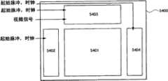
图12所示的信号线驱动器电路包括:驱动器IC 5601;开关群5602_1至5602_M;第一布线5611;第二布线5612;第三布线5613;以及布线5621_1至5621_M。开关群5602_1至5602_M的每一个包括第一薄膜晶体管5603a、第二薄膜晶体管5603b以及第三薄膜晶体管5603c。The signal line driver circuit shown in FIG. 12 includes: a
驱动器IC 5601连接到第一布线5611、第二布线5612、第三布线5613及布线5621_1至5621_M。而且,开关群5602_1至5602_M的每一个分别连接到第一布线5611、第二布线5612、第三布线5613及分别对应于开关群5602_1至5602_M的布线5621_1至5621_M之一。而且,布线5621_1至5621_M的每一个通过第一薄膜晶体管5603a、第二薄膜晶体管5603b及第三薄膜晶体管5603c连接到三条信号线。例如,第J列的布线5621_J(布线5621_1至5621_M中的任一条)通过开关群5602_J所具有的第一薄膜晶体管5603a、第二薄膜晶体管5603b及第三薄膜晶体管5603c连接到信号线Sj-1、信号线Sj、信号线Sj+1。The
注意,对第一布线5611、第二布线5612、第三布线5613分别输入信号。Note that signals are respectively input to the
注意,驱动器IC 5601优选形成在单晶衬底上。再者,开关群5602_1至5602_M优选与像素部形成在同一衬底上。因此,通过FPC等将驱动器IC 5601连接到开关群5602_1至5602_M。Note that the
接着,参照图13的时序图说明图12所示的信号线驱动器电路的操作。注意,图13的时序图示出选择第i行扫描线Gi时的时序图。第i行扫描线Gi的选择周期被分割为第一子选择周期T1、第二子选择周期T2及第三子选择周期T3。而且,在选择其他行的扫描线的情况下,图12的信号线驱动器电路也进行与图13类似的操作。Next, the operation of the signal line driver circuit shown in FIG. 12 will be described with reference to the timing chart of FIG. 13 . Note that the timing chart of FIG. 13 shows a timing chart when the scanning line Gi of the i-th row is selected. The selection period of the i-th scan line Gi is divided into a first sub-selection period T1, a second sub-selection period T2, and a third sub-selection period T3. Also, the signal line driver circuit of FIG. 12 performs operations similar to those of FIG. 13 in the case of selecting a scanning line of another row.
注意,图13的时序图示出第J列布线5621_J分别通过第一薄膜晶体管5603a、第二薄膜晶体管5603b及第三薄膜晶体管5603c连接到信号线Sj-1、信号线Sj、信号线Sj+1的情况。Note that the timing diagram in FIG. 13 shows that the J-th column wiring 5621_J is connected to the signal line Sj-1, the signal line Sj, and the signal line Sj+1 through the first
图13的时序图示出第i行扫描线Gi被选择的时序、第一薄膜晶体管5603a的导通/截止的时序5703a、第二薄膜晶体管5603b的导通/截止的时序5703b、第三薄膜晶体管5603c的导通/截止的时序5703c以及输入到第J列布线5621_J的信号5721_J。The timing diagram in FIG. 13 shows the timing when the i-th scan line Gi is selected, the timing 5703a of turning on/off the first
在第一子选择周期T1、第二子选择周期T2及第三子选择周期T3中,向布线5621_1至布线5621_M输入不同的视频信号。例如,在第一子选择周期T1中输入到布线5621_J的视频信号输入到信号线Sj-1,在第二子选择周期T2中输入到布线5621_J的视频信号输入到信号线Sj,并且在第三子选择周期T3中输入到布线5621_J的视频信号输入到信号线Sj+1。再者,在第一子选择周期T1、第二子选择周期T2及第三子选择周期T3中输入到布线5621_J的视频信号为数据_j-1、数据_j、数据_j+1。In the first sub-selection period T1, the second sub-selection period T2, and the third sub-selection period T3, different video signals are input to the wiring 5621_1 to the wiring 5621_M. For example, the video signal input to the wiring 5621_J in the first sub-selection period T1 is input to the signal line Sj-1, the video signal input to the wiring 5621_J in the second sub-selection period T2 is input to the signal line Sj, and The video signal input to the wiring 5621_J in the sub-selection period T3 is input to the signal
如图13所示,在第一子选择周期T1中,第一薄膜晶体管5603a导通,而第二薄膜晶体管5603b及第三薄膜晶体管5603c截止。此时,输入到布线5621_J的数据_j-1通过第一薄膜晶体管5603a输入到信号线Sj-1。在第二子选择周期T2中,第二薄膜晶体管5603b导通,而第一薄膜晶体管5603a及第三薄膜晶体管5603c截止。此时,输入到布线5621_J的数据_j通过第二薄膜晶体管5603b输入到信号线Sj。在第三子选择周期T3中,第三薄膜晶体管5603c导通,而第一薄膜晶体管5603a及第二薄膜晶体管5603b截止。此时,输入到布线5621_J的数据_j+1通过第三薄膜晶体管5603c输入到信号线Sj+1。As shown in FIG. 13, in the first sub-selection period T1, the first
如上所述,图12的信号线驱动器电路通过将一个门选择周期分割为三个来可以在一个门选择周期中将视频信号从一条布线5621输入到三条信号线。因此,图12的信号线驱动器电路中,设置有驱动器IC 5601的衬底和设置有像素部的衬底的连接数可约为信号线数的1/3。因为连接数减少为信号线数的大约1/3,图12的信号线驱动器电路可提高可靠性、成品率等。As described above, the signal line driver circuit of FIG. 12 can input video signals from one wiring 5621 to three signal lines in one gate selection period by dividing one gate selection period into three. Therefore, in the signal line driver circuit of FIG. 12, the number of connections between the substrate on which the
注意,只要能够如图12所示,将一个门选择周期分割为多个子选择周期,并在各子选择周期中从某一条布线向多条信号线分别输入视频信号,就对于薄膜晶体管的排列、数量及驱动方法等没有特别的限制。Note that as long as one gate selection period can be divided into multiple sub-selection periods as shown in FIG. The number, driving method, and the like are not particularly limited.
例如,当在三个或以上的子选择周期的每一个周期中从一条布线将视频信号分别输入到三条或以上的信号线时,追加薄膜晶体管及用于控制薄膜晶体管的布线即可。注意,当将一个门选择周期分割为四个或以上的子选择周期时,一个子选择周期变得更短。因此,优选将一个门选择周期分割为两个或三个子选择周期。For example, when video signals are input from one wiring to three or more signal lines in each of three or more sub-selection periods, it is sufficient to add thin film transistors and wiring for controlling the thin film transistors. Note that when one gate selection period is divided into four or more sub-selection periods, one sub-selection period becomes shorter. Therefore, it is preferable to divide one gate selection period into two or three sub-selection periods.
作为另一示例,也可如图14的时序图所示,将一个选择周期分割为预充电周期Tp、第一子选择周期T1、第二子选择周期T2、第三子选择周期T3。图14的时序图示出选择第i行扫描线Gi的时序、第一薄膜晶体管5603a的导通/截止的时序5803a、第二薄膜晶体管5603b的导通/截止的时序5803b、第三薄膜晶体管5603c的导通/截止的时序5803c以及输入到第J列布线5621_J的信号5821_J。如图14所示,在预充电周期Tp中,第一薄膜晶体管5603a、第二薄膜晶体管5603b及第三薄膜晶体管5603c导通。此时,输入到布线5621_J的预充电电压Vp通过第一薄膜晶体管5603a、第二薄膜晶体管5603b及第三薄膜晶体管5603c输入到信号线Sj-1、信号线Sj、信号线Sj+1。在第一子选择周期T1中,第一薄膜晶体管5603a导通,而第二薄膜晶体管5603b及第三薄膜晶体管5603c截止。此时,输入到布线5621_J的数据_j-1通过第一薄膜晶体管5603a输入到信号线Sj-1。在第二子选择周期T2中,第二薄膜晶体管5603b导通,而第一薄膜晶体管5603a及第三薄膜晶体管5603c截止。此时,输入到布线5621_J的数据_j通过第二薄膜晶体管5603b输入到信号线Sj。在第三子选择周期T3中,第三薄膜晶体管5603c导通,而第一薄膜晶体管5603a及第二薄膜晶体管5603b截止。此时,输入到布线5621_J的数据_j+1通过第三薄膜晶体管5603c输入到信号线Sj+1。As another example, as shown in the timing diagram of FIG. 14 , one selection period may be divided into a precharge period Tp, a first sub-selection period T1 , a second sub-selection period T2 , and a third sub-selection period T3 . The timing diagram in FIG. 14 shows the timing of selecting the i-th scan line Gi, the timing 5803a of turning on/off the first
如上所述,应用图14的时序图的图12的信号线驱动器电路中,可通过在子选择周期之前提供预充电选择周期来对信号线进行预充电,因此可高速地对像素写入视频信号。注意,在图14中,使用共同的附图标记来表示与图13类似的部分,而省略对于相同的部分以及具有相同功能的部分的详细说明。As described above, in the signal line driver circuit of FIG. 12 to which the timing chart of FIG. 14 is applied, the signal line can be precharged by providing the precharge selection period before the subselection period, so that the video signal can be written to the pixel at high speed. . Note that in FIG. 14 , parts similar to those in FIG. 13 are denoted by common reference numerals, and detailed descriptions of the same parts and parts having the same functions are omitted.
此外,说明扫描线驱动器电路的结构。扫描线驱动器电路包括移位寄存器及缓冲器。此外,根据情况,扫描线驱动器电路还可包括电平移动器。在扫描线驱动器电路中,对移位寄存器输入时钟信号(CLK)及起始脉冲信号(SP)时生成选择信号。所生成的选择信号被缓冲器缓冲和放大,并将所得信号供给到对应的扫描线。扫描线连接到一条线的像素中的晶体管的栅电极。而且,由于需要将一条线的像素的诸晶体管一齐导通,因此使用能够馈送大电流的缓冲器。In addition, the configuration of the scanning line driver circuit will be described. The scan line driver circuit includes a shift register and a buffer. In addition, the scan line driver circuit may further include a level shifter according to circumstances. In the scanning line driver circuit, a selection signal is generated when a clock signal (CLK) and a start pulse signal (SP) are input to the shift register. The generated selection signal is buffered and amplified by the buffer, and the resulting signal is supplied to the corresponding scan line. The scan lines are connected to the gate electrodes of the transistors in the pixels of one line. Also, since it is necessary to turn on transistors of pixels of one line at a time, a buffer capable of feeding a large current is used.
参照图15和图16说明用于扫描线驱动器电路的一部分的移位寄存器的一个模式。One mode of the shift register used for a part of the scanning line driver circuit will be described with reference to FIGS. 15 and 16 .
图15示出移位寄存器的电路结构。图15所示的移位寄存器包括多个触发器(触发器5701_1至5701_n)。该移位寄存器通过输入第一时钟信号、第二时钟信号、起始脉冲信号、复位信号来进行工作。Fig. 15 shows the circuit structure of the shift register. The shift register shown in FIG. 15 includes a plurality of flip-flops (flip-flops 5701_1 to 5701_n). The shift register operates by inputting a first clock signal, a second clock signal, a start pulse signal and a reset signal.
说明图15的移位寄存器的连接关系。在图15的移位寄存器的第i级触发器5701_i(触发器5701_1至5701_n中的任一个)中,图16所示的第一布线5501连接到第七布线5717_i-1;图16所示的第二布线5502连接到第七布线5717_i+1;图16所示的第三布线5503连接到第七布线5717_i;并且图16所示的第六布线5506连接到第五布线5715。The connection relation of the shift register in Fig. 15 will be described. In the i-th stage flip-flop 5701_i (any one of flip-flops 5701_1 to 5701_n) of the shift register in FIG. 15 , the
此外,在奇数级的触发器中图16所示的第四布线5504连接到第二布线5712,在偶数级的触发器中其连接到第三布线5713。图16所示的第五布线5505连接到第四布线5714。Further, the
注意,第一级触发器5701_1的图16所示的第一布线5501连接到第一布线5711。此外,第n级触发器5701_n的图16所示的第二布线5502连接到第六布线5716。Note that the
注意,第一布线5711、第二布线5712、第三布线5713、第六布线5716也可分别称为第一信号线、第二信号线、第三信号线、第四信号线。第四布线5714、第五布线5715可分别称为第一电源线、第二电源线。Note that the
接着,图16示出图15所示的触发器的详细结构。图16所示的触发器包括第一薄膜晶体管5571、第二薄膜晶体管5572、第三薄膜晶体管5573、第四薄膜晶体管5574、第五薄膜晶体管5575、第六薄膜晶体管5576、第七薄膜晶体管5577以及第八薄膜晶体管5578。注意,第一薄膜晶体管5571、第二薄膜晶体管5572、第三薄膜晶体管5573、第四薄膜晶体管5574、第五薄膜晶体管5575、第六薄膜晶体管5576、第七薄膜晶体管5577以及第八薄膜晶体管5578的每一个是n沟道晶体管,并且当栅极-源极间电压(Vgs)超过阈值电压(Vth)时导通。Next, FIG. 16 shows the detailed structure of the flip-flop shown in FIG. 15 . The trigger shown in FIG. 16 includes a first
接着,下面示出图16所示的触发器的连接结构。Next, the connection structure of the flip-flop shown in FIG. 16 is shown below.
第一薄膜晶体管5571的第一电极(源电极及漏电极中的一个)连接到第四布线5504。第一薄膜晶体管5571的第二电极(源电极及漏电极中的另一个)连接到第三布线5503。The first electrode (one of the source electrode and the drain electrode) of the first
第二薄膜晶体管5572的第一电极连接到第六布线5506。第二薄膜晶体管5572的第二电极连接到第三布线5503。The first electrode of the second
第三薄膜晶体管5573的第一电极连接到第五布线5505。第三薄膜晶体管5573的第二电极连接到第二薄膜晶体管5572的栅电极。第三薄膜晶体管5573的栅电极连接到第五布线5505。The first electrode of the third
第四薄膜晶体管5574的第一电极连接到第六布线5506。第四薄膜晶体管5574的第二电极连接到第二薄膜晶体管5572的栅电极。第四薄膜晶体管5574的栅电极连接到第一薄膜晶体管5571的栅电极。The first electrode of the fourth
第五薄膜晶体管5575的第一电极连接到第五布线5505。第五薄膜晶体管5575的第二电极连接到第一薄膜晶体管5571的栅电极。第五薄膜晶体管5575的栅电极连接到第一布线5501。The first electrode of the fifth
第六薄膜晶体管5576的第一电极连接到第六布线5506。第六薄膜晶体管5576的第二电极连接到第一薄膜晶体管5571的栅电极。第六薄膜晶体管5576的栅电极连接到第二薄膜晶体管5572的栅电极。The first electrode of the sixth
第七薄膜晶体管5577的第一电极连接到第六布线5506。第七薄膜晶体管5577的第二电极连接到第一薄膜晶体管5571的栅电极。第七薄膜晶体管5577的栅电极连接到第二布线5502。第八薄膜晶体管5578的第一电极连接到第六布线5506。第八薄膜晶体管5578的第二电极连接到第二薄膜晶体管5572的栅电极。第八薄膜晶体管5578的栅电极连接到第一布线5501。The first electrode of the seventh
注意,第一薄膜晶体管5571的栅电极、第四薄膜晶体管5574的栅电极、第五薄膜晶体管5575的第二电极、第六薄膜晶体管5576的第二电极以及第七薄膜晶体管5577的第二电极所连接的点称作节点5543。第二薄膜晶体管5572的栅电极、第三薄膜晶体管5573的第二电极、第四薄膜晶体管5574的第二电极、第六薄膜晶体管5576的栅电极以及第八薄膜晶体管5578的第二电极所连接的点称作节点5544。Note that the gate electrode of the first
注意,第一布线5501、第二布线5502、第三布线5503以及第四布线5504可分别称为第一信号线、第二信号线、第三信号线、第四信号线。第五布线5505、第六布线5506可分别称为第一电源线、第二电源线。Note that the
此外,也可仅使用可以与实施例2或3所示的非线性元件一起并以类似方法形成的n沟道TFT来制造信号线驱动器电路及扫描线驱动器电路。因为可以与实施例2或3所示的非线性元件一起并以类似方法形成的n沟道TFT具有高迁移率,所以可提高驱动器电路的驱动频率。另外,由于可以与实施例2或3所示的非线性元件一起并以类似方法形成的n沟道TFT包括利用包含铟、镓及锌的氧缺乏氧化物半导体层形成的源区或漏区,因此减小寄生电容,并增大频率特性(称为f特性)。例如,由于包括可以与实施例2或3所示的非线性元件一起并以类似的方法形成的n沟道TFT的扫描线驱动器电路可高速工作,因此可提高帧频率或实现例如黑屏插入等。In addition, the signal line driver circuit and the scanning line driver circuit can also be manufactured using only n-channel TFTs that can be formed together with the nonlinear element shown in
再者,例如,增大扫描线驱动器电路的晶体管的沟道宽度,或设置多个扫描线驱动器电路时,可实现更高的帧频率。在设置多个扫描线驱动器电路的情况下,用于驱动偶数扫描线的扫描线驱动器电路设置在一侧,用于驱动奇数扫描线的扫描线驱动器电路配置在其相反一侧;因此可实现帧频率的增大。Furthermore, for example, a higher frame frequency can be realized by increasing the channel width of the transistor of the scanning line driver circuit or by providing a plurality of scanning line driver circuits. In the case where a plurality of scanning line driver circuits are provided, the scanning line driver circuits for driving the even scanning lines are arranged on one side, and the scanning line driver circuits for driving the odd scanning lines are arranged on the opposite side; therefore, frame increase in frequency.
在制造根据本发明一实施例的半导体装置的一示例的有源矩阵型发光显示装置的情况下,因为至少在一个像素中安排多个薄膜晶体管,因此优选安排多个扫描线驱动器电路。图11B示出有源矩阵型发光显示装置的框图的一示例。In the case of manufacturing an active matrix type light emitting display device which is an example of a semiconductor device according to an embodiment of the present invention, since a plurality of thin film transistors are arranged in at least one pixel, it is preferable to arrange a plurality of scanning line driver circuits. FIG. 11B shows an example of a block diagram of an active matrix type light emitting display device.
图11B所示的发光显示装置在衬底5400上包括:包括各设置有显示元件的多个像素的像素部5401;选择各像素的第一扫描线驱动器电路5402及第二扫描线驱动器电路5404;以及控制对所选像素的视频信号输入的信号线驱动器电路5403。The light-emitting display device shown in FIG. 11B includes on a substrate 5400: a
在向图11B所示的发光显示装置的像素输入数字视频信号的情况下,通过切换晶体管的导通和截止,像素处于发光或非发光状态。因此,可以采用面积比灰度法或时间比灰度法显示灰度级。面积比灰度法是一种驱动法,其中通过将一个像素分割为多个子像素并基于视频信号分别驱动各子像素,从而显示灰度级。此外,时间比灰度法是一种驱动法,其中通过控制像素发光的期间来显示灰度级。In the case where a digital video signal is input to a pixel of the light-emitting display device shown in FIG. 11B , the pixel is in a light-emitting or non-light-emitting state by switching the transistor on and off. Therefore, the area ratio grayscale method or the time ratio grayscale method can be used to display gray levels. The area ratio gradation method is a driving method in which gradation is displayed by dividing one pixel into a plurality of sub-pixels and driving each sub-pixel individually based on a video signal. In addition, the time-ratio grayscale method is a driving method in which grayscale is displayed by controlling the period during which pixels emit light.
因为发光元件的响应时间比液晶元件等短,所以发光元件适合于时间比灰度法。具体而言,通过时间比灰度法进行显示的情况下,将一个帧周期分割为多个子帧周期。然后,响应于视频信号,在各子帧周期中使像素的发光元件处于发光或非发光状态。通过将一个帧周期分割为多个子帧周期,可利用视频信号控制在一个帧周期中像素实际上发光的时间的总长度,以显示灰度级。Since the response time of the light-emitting element is shorter than that of a liquid crystal element, etc., the light-emitting element is suitable for the time-ratio grayscale method. Specifically, when performing display by the time ratio grayscale method, one frame period is divided into a plurality of subframe periods. Then, in response to the video signal, the light-emitting element of the pixel is made to be in a light-emitting or non-light-emitting state in each sub-frame period. By dividing one frame period into a plurality of subframe periods, the video signal can be used to control the total length of time during which pixels actually emit light in one frame period to display grayscale.
注意,在图11B所示的发光显示装置中,其中一个像素包括两个TFT(即开关TFT和电流控制TFT)的情况下,使用第一扫描线驱动器电路5402生成输入到作为开关TFT的栅极布线的第一扫描线的信号,而使用第二扫描线驱动器电路5404生成输入到作为电流控制TFT的栅极布线的第二扫描线的信号。但是,可使用一个扫描线驱动器电路生成输入到第一扫描线的信号和输入到第二扫描线的信号。此外,例如根据开关元件所具有的各晶体管的数量,可能会在各像素中设置用来控制开关元件的工作的多个第一扫描线。在此情况下,既可使用一个扫描线驱动器电路生成输入到多条第一扫描线的所有信号,又可使用多个扫描线驱动器电路生成输入到多条第一扫描线的所有信号。Note that in the light-emitting display device shown in FIG. 11B , where one pixel includes two TFTs (that is, a switching TFT and a current control TFT), the first scanning
即使在发光显示装置中,可将能够由n沟道TFT形成的驱动器电路的一部分与像素部的薄膜晶体管设置在同一衬底上。另外,也可仅使用可以与实施例2或3所示的非线性元件一起并以类似的方法形成的n沟道TFT来制造信号线驱动器电路及扫描线驱动器电路。Even in a light-emitting display device, a part of a driver circuit that can be formed by an n-channel TFT can be provided on the same substrate as a thin film transistor in a pixel portion. In addition, the signal line driver circuit and the scanning line driver circuit can also be manufactured using only n-channel TFTs that can be formed in a similar manner with the nonlinear element shown in
上述驱动器电路除了用于液晶显示装置及发光显示装置以外还可用于利用电连接至开关元件的元件来驱动电子墨水的电子纸。电子纸也称为电泳显示装置(电泳显示器),并具有如下优点:与普通纸相同级别的可读性、功耗比其他显示装置低、可形成为薄且轻的形状。The driver circuit described above can be used in electronic paper that drives electronic ink using an element electrically connected to a switching element in addition to the liquid crystal display device and the light emitting display device. Electronic paper is also called an electrophoretic display device (electrophoretic display), and has advantages of the same level of readability as plain paper, lower power consumption than other display devices, and can be formed into a thin and light shape.
电泳显示器可具有各种模式。电泳显示器包含,在溶剂或溶质中分散的多个微囊,各微囊包含带正电的第一粒子和带负电的第二粒子。通过对微囊施加电场,使微囊中的粒子向相反方向移动,并仅显示集合在一侧的粒子的颜色。注意,第一粒子和第二粒子各包含色素,且在没有电场时不移动。此外,第一粒子和第二粒子的颜色相互不同(颜色包括无色或色素缺乏)。Electrophoretic displays are available in various modes. The electrophoretic display comprises a plurality of microcapsules dispersed in a solvent or solute, each microcapsule comprising positively charged first particles and negatively charged second particles. By applying an electric field to the microcapsule, the particles in the microcapsule move in opposite directions, and only the color of the particles gathered on one side is displayed. Note that each of the first particle and the second particle contains a pigment, and does not move in the absence of an electric field. In addition, the colors of the first particles and the second particles are different from each other (the colors include colorless or lack of pigment).
像这样,电泳显示器是利用所谓的介电电泳效应的显示器,其中由介电常数高的物质移动到高电场区。电泳显示器不需要液晶显示装置所需的偏振片和反衬底,从而可使电泳显示器厚度和重量为液晶显示装置的一半。As such, an electrophoretic display is a display utilizing the so-called dielectrophoretic effect in which a substance with a high dielectric constant moves to a high electric field region. The electrophoretic display does not require the polarizer and the anti-substrate required by the liquid crystal display device, so that the thickness and weight of the electrophoretic display can be half of that of the liquid crystal display device.
将在溶剂中分散有上述微囊的溶液称作电子墨水。该电子墨水可印刷到玻璃、塑料、布、纸等的表面上。另外,还可通过使用滤色片或具有色素的粒子来进行彩色显示。A solution in which the above microcapsules are dispersed in a solvent is called electronic ink. The electronic ink can be printed onto surfaces of glass, plastic, cloth, paper, and the like. In addition, color display can also be performed by using color filters or particles with pigments.
此外,通过在有源矩阵衬底上适当地设置多个微囊以使微囊夹在两个电极之间,从而完成有源矩阵型显示装置,并且对微囊施加电场可进行显示。例如,可使用利用薄膜晶体管获得的有源矩阵衬底,其中薄膜晶体管可以与实施例2或3所示的非线性元件一起并以制造非线性元件类似的方法形成。Furthermore, an active matrix type display device is completed by appropriately disposing a plurality of microcapsules on an active matrix substrate so that the microcapsules are sandwiched between two electrodes, and display can be performed by applying an electric field to the microcapsules. For example, an active matrix substrate obtained by using a thin film transistor which can be formed together with the nonlinear element shown in
注意,微囊中的第一粒子及第二粒子可选自以下材料之一来形成,导电材料、绝缘材料、半导体材料、磁性材料、液晶材料、铁电材料、电致发光材料、电致变色材料、磁泳材料或这些材料的组合材料。Note that the first particle and the second particle in the microcapsule can be formed from one of the following materials, conductive material, insulating material, semiconductor material, magnetic material, liquid crystal material, ferroelectric material, electroluminescent material, electrochromic material, magnetophoretic material, or a combination of these materials.
根据上述步骤,在非线性元件的第一氧化物半导体层与布线层的连接结构中,设置与其导电率高于第一氧化物半导体层的导电率的第二氧化物半导体层接合的区域、或设置通过等离子体处理改良的区域,这与只采用金属布线的情况相比,可允许稳定工作。由此,可增强保护电路的功能并实现工作的稳定化。此外,可通过包括具有不容易产生归因于膜剥离的缺陷的非线性元件的保护电路来制造稳定工作的可靠性高的显示装置。According to the above steps, in the connection structure between the first oxide semiconductor layer and the wiring layer of the nonlinear element, a region joined to the second oxide semiconductor layer having a higher conductivity than the first oxide semiconductor layer is provided, or An area improved by plasma treatment is provided, which allows stable operation compared to the case of using only metal wiring. Thus, the function of the protection circuit can be enhanced and the operation can be stabilized. In addition, a high-reliability display device that operates stably can be manufactured by including a protection circuit having a nonlinear element that does not easily generate defects due to film peeling.
实施例5可与其他实施例的结构适当地组合而实施。Embodiment 5 can be implemented in combination with structures of other embodiments as appropriate.
实施例6Example 6
根据本发明的一实施例可与非线性元件一起制造薄膜晶体管并将该薄膜晶体管用于像素部并进一步用于驱动器电路,从而可制造具有显示功能的半导体装置(也称为显示装置)。此外,根据本发明一实施例的非线性元件和薄膜晶体管可用于与像素部一起形成在一个衬底上的驱动器电路的一部分或整体驱动器电路,从而形成面板上系统(system-on-panel)。According to an embodiment of the present invention, a thin film transistor can be manufactured together with a nonlinear element, and the thin film transistor can be used in a pixel portion and further used in a driver circuit, so that a semiconductor device having a display function (also called a display device) can be manufactured. In addition, a nonlinear element and a thin film transistor according to an embodiment of the present invention can be used for a part of a driver circuit or an entire driver circuit formed on one substrate together with a pixel portion, thereby forming a system-on-panel.
显示装置包括显示元件。作为显示元件,可使用液晶元件(也称为液晶显示元件)、或发光元件(也称为发光显示元件)。在发光元件的范围内包括利用电流或电压控制亮度的元件,具体而言,包括无机电致发光(EL)元件、有机EL元件等。此外,可应用电子墨水等的对比度因电作用而变化的显示介质。The display device includes a display element. As a display element, a liquid crystal element (also called a liquid crystal display element) or a light emitting element (also called a light emitting display element) can be used. The light-emitting element includes elements that control luminance by current or voltage, specifically, inorganic electroluminescence (EL) elements, organic EL elements, and the like. In addition, a display medium whose contrast is changed by electricity, such as electronic ink, can be applied.
此外,显示装置包括密封有显示元件的面板和在该面板上的安装有包括控制器的IC等的模块。本发明的一实施例涉及制造该显示装置的过程中的显示元件完成之前的元件衬底的一模式,并且该元件衬底设置有用于向多个像素的每一个中的显示元件供应电流的装置。具体而言,元件衬底可以是只设置有显示元件像素电极的状态、成为像素电极的导电膜形成之后且导电膜被蚀刻形成像素电极之前的状态、或其它任何状态。In addition, the display device includes a panel in which a display element is sealed and a module on which an IC including a controller and the like are mounted. An embodiment of the present invention relates to a mode of an element substrate before a display element is completed in a process of manufacturing the display device, and the element substrate is provided with means for supplying current to a display element in each of a plurality of pixels . Specifically, the element substrate may be in the state where only the pixel electrodes of the display element are provided, after the conductive film to be the pixel electrode is formed and before the conductive film is etched to form the pixel electrode, or in any other state.
本说明书中的显示装置是指图像显示装置、显示装置、或光源(包括照明装置)。另外,显示装置在其范畴中包括任一以下模块:包括诸如柔性印刷电路(FPC)、带式自动接合(TAB)带、或带式载体封装(TCP)的连接器的模块;具有在其端部设置有印刷线路板的TAB带或TCP的模块;以及具有通过玻璃上芯片(COG)方法在显示元件上直接安装的集成电路(IC)的模块。The display device in this specification refers to an image display device, a display device, or a light source (including a lighting device). In addition, the display device includes any of the following modules in its category: a module including a connector such as a flexible printed circuit (FPC), a tape automated bonding (TAB) tape, or a tape carrier package (TCP); a module having a TAB tape or TCP provided with a printed wiring board on the inside; and a module having an integrated circuit (IC) directly mounted on a display element by a chip-on-glass (COG) method.
在实施例6中,参照图17A和17B说明根据本发明一实施例的显示装置的一模式的液晶显示面板的外观及截面。图17A是一面板的俯视图,其中利用密封材料4005由第二衬底4006将可以与非线性元件一起并以制造非线性元件类似的方法形成的电特性高的薄膜晶体管4010、4011,以及液晶元件4013密封。图17B相当于沿着图17A-1、17A-2的M-N的截面。In Embodiment 6, the appearance and cross section of a liquid crystal display panel of a mode of a display device according to an embodiment of the present invention will be described with reference to FIGS. 17A and 17B. Fig. 17A is a top view of a panel, in which
以包围设置在第一衬底4001上的像素部4002和扫描线驱动器电路4004的方式设置密封材料4005。在像素部4002和扫描线驱动器电路4004上设置有第二衬底4006。因此,用密封材料将像素部4002和扫描线驱动器电路4004与液晶层4008密封在第一衬底4001和第二衬底4006之间。此外,在与第一衬底4001上的由密封材料4005包围的区域不同的区域中安装有信号线驱动器电路4003,其中另行制备的信号线驱动器电路4003在衬底上使用单晶半导体膜或多晶半导体膜形成。A sealing
注意,对于另行形成的驱动器电路的连接方法没有特别的限制,且可采用COG方法、引线接合方法或TAB方法等。图17A-1示出通过COG方法安装信号线驱动器电路4003的示例,而图17A-2示出通过TAB方法安装信号线驱动器电路4003的示例。Note that there is no particular limitation on the connection method of the separately formed driver circuit, and a COG method, a wire bonding method, a TAB method, or the like may be employed. 17A-1 shows an example of mounting the signal
设置在第一衬底4001上的像素部4002和扫描线驱动器电路4004包括多个薄膜晶体管。图17B示出像素部4002所包括的薄膜晶体管4010和扫描线驱动器电路4004所包括的薄膜晶体管4011。在薄膜晶体管4010、4011上设置有绝缘层4020、4021。The
薄膜晶体管4010、4011各具有高电特性,其中包含In、Ga及Zn的氧化物半导体用于半导体层及源区及漏区,并可以应用与实施例2或3所示的非线性元件一起并以类似的方法形成。在实施例6中,薄膜晶体管4010、4011是n沟道薄膜晶体管。The
液晶元件4013所包括的像素电极层4030电连接至薄膜晶体管4010。液晶元件4013的反电极层4031形成在第二衬底4006上。像素电极层4030、反电极层4031和液晶层4008重叠的部分对应于液晶元件4013。注意,像素电极层4030、反电极层4031分别设置有用作取向膜的绝缘层4032、4033,且像素电极层4030和反电极层4031之间有绝缘层4032和4033,且在绝缘层4032和4033之间有液晶层4008。The
注意,第一衬底4001、第二衬底4006可使用玻璃、金属(典型为不锈钢)、陶瓷、塑料形成。作为塑料可使用玻璃纤维增强塑料(FRP)板、聚氟乙烯(PVF)膜、聚酯膜或丙烯酸树脂膜。此外,还可使用具有将铝箔夹在PVF膜及聚酯膜之间的结构的薄片。Note that the
此外,设置通过选择性地蚀刻绝缘膜形成的柱状隔离件4035以控制像素电极层4030和反电极层4031之间的距离(单元间隙)。替代地,还可使用球状隔离件。In addition, a
另外,还可使用不使用取向膜的蓝相液晶。蓝相是液晶相的一种,是指当使胆甾液晶的温度上升时即将从胆甾液晶转变到各向同性相之前出现的相。由于蓝相只出现在较窄的温度范围内,所以为了扩大温度范围,使用混合有5重量%或以上的手性试剂的液晶组合物来形成液晶层4008。包含蓝相液晶和手性试剂的液晶组合物的响应时间短于10μs至100μs,并且由于其具有光学各向同性,因此不需要取向处理且视角依赖小。In addition, blue phase liquid crystals that do not use an alignment film can also be used. The blue phase is one type of liquid crystal phase, and refers to a phase that appears just before the transition from the cholesteric liquid crystal to the isotropic phase when the temperature of the cholesteric liquid crystal is raised. Since the blue phase appears only in a narrow temperature range, in order to expand the temperature range, the
另外,虽然实施例6示出透射型液晶显示装置的示例,但是本发明的一实施例既可应用于反射型液晶显示装置,又可应用于半透射型液晶显示装置。In addition, although Embodiment 6 shows an example of a transmissive type liquid crystal display device, an embodiment of the present invention can be applied to both a reflective type liquid crystal display device and a transflective type liquid crystal display device.
另外,虽然实施例6的液晶显示装置中,在衬底外侧(观看者一侧)设置偏振片,并在衬底内侧设置显示元件的着色层和电极层,它们以该顺序排列,但是也可在衬底内侧设置偏振片。另外,偏振片和着色层的叠层结构不限于实施例6的结构,且根据偏振片和着色层的材料以及制造工序条件适当地设定即可。另外,还可设置用作黑矩阵的遮光膜。In addition, although in the liquid crystal display device of Example 6, the polarizing plate is provided on the outside of the substrate (the viewer's side), and the colored layer and the electrode layer of the display element are provided on the inside of the substrate, they are arranged in this order, but it may also be A polarizer is provided inside the substrate. In addition, the lamination structure of the polarizing plate and the colored layer is not limited to the structure of Example 6, and may be appropriately set according to the materials of the polarizing plate and the colored layer and the conditions of the manufacturing process. In addition, a light-shielding film serving as a black matrix may also be provided.
在实施例6中,使用保护膜或用作平坦化绝缘膜的绝缘层(绝缘层4020、绝缘层4021)覆盖实施例2或3所示的非线性元件、以及可以与非线性元件一起并以类似的方法形成的薄膜晶体管,以降低薄膜晶体管的表面不平坦并提高薄膜晶体管的可靠性。注意,设置保护膜用来防止诸如大气中的有机物质、金属物质、水分的污染杂质的侵入,所以优选采用致密膜。保护膜可使用氧化硅膜、氮化硅膜、氧氮化硅膜或氮氧化硅膜、氧化铝膜、氮化铝膜、氧氮化铝膜或氮氧化铝膜的单层或叠层来形成。虽然在实施例6中利用溅射法形成保护膜,但是该方法不限于特定方法并可选自各种方法。In Embodiment 6, the nonlinear element shown in
在此,形成叠层结构的绝缘层4020作为保护膜。在此,利用溅射法形成氧化硅膜作为绝缘层4020的第一层。当作为保护膜使用氧化硅膜提供防止用作源电极层及漏电极层的铝膜小丘的有益效果。Here, the insulating
另外,形成绝缘层作为保护膜的第二层。在此,利用溅射法形成氮化硅膜作为绝缘层4020的第二层。当使用氮化硅膜作为保护膜时,可抑制钠等的可动离子侵入到半导体区域中而使TFT的电特性变化。In addition, an insulating layer is formed as a second layer of the protective film. Here, a silicon nitride film is formed as the second layer of the insulating
另外,可在形成保护膜之后进行对IGZO半导体层的退火(300℃至400℃)。In addition, annealing (300° C. to 400° C.) of the IGZO semiconductor layer may be performed after forming the protective film.
另外,形成绝缘层4021作为平坦化绝缘膜。该绝缘层4021可形成自具有耐热性的有机材料如聚酰亚胺、丙烯酸、苯并环丁烯、聚酰胺、环氧等。另外,作为上述有机材料的替代,可使用低介电常数材料(low-k材料)、硅氧烷基树脂、PSG(磷硅玻璃)、BPSG(硼磷硅玻璃)等。硅氧烷基树脂除了氢之外还可包括氟、烷基或芳基中的至少一种作为取代基。另外,可通过层叠多个由这些材料形成的绝缘膜来形成绝缘层4021。In addition, an insulating
另外,硅氧烷基树脂是以硅氧烷基材料为起始材料而形成的具有Si-O-Si键的树脂。硅氧烷基树脂除了氢以外,可具有氟、烷基或芳香烃中的至少一种作为取代基。In addition, the siloxane-based resin is a resin having a Si-O-Si bond formed from a siloxane-based material as a starting material. The siloxane-based resin may have at least one of fluorine, an alkyl group, or an aromatic hydrocarbon as a substituent in addition to hydrogen.
对绝缘层4021的形成方法没有特别的限制,可根据绝缘层4021的材料使用以下方法:溅射法、SOG法、旋涂、浸涂、喷涂、液滴放电法(例如,喷墨法、丝网印刷、胶版印刷等)、刮片、辊涂、幕涂、刀涂等。在使用材料液形成绝缘层4021的情况下,可在进行烘焙的步骤中同时进行对IGZO半导体层的退火(300℃至400℃)。通过兼作绝缘层4021的烘焙和对IGZO半导体层的退火,可有效地制造半导体装置。The method for forming the insulating
像素电极层4030和反电极层4031可使用诸如包含氧化钨的氧化铟、包含氧化钨的氧化铟锌、包含氧化钛的氧化铟、包含氧化钛的氧化铟锡、氧化铟锡(下面表示为ITO)、氧化铟锌、添加有氧化硅的氧化铟锡的透光导电材料来形成。The
可使用包含导电高分子(也称为导电聚合物)的导电组合物形成像素电极层4030、反电极层4031。使用导电组合物形成的像素电极的薄层电阻优选为10000Ω/□或更小,并且波长为550nm时的透光率优选为70%或更高。另外,导电组合物所包含的导电高分子的电阻率优选为0.1Ω·cm或更小。The
作为导电高分子,可使用所谓的π电子共轭类导电高分子。例如,可举出聚苯胺或其衍生物、聚吡咯或其衍生物、聚噻吩或其衍生物、或者上述材料中的两种以上的共聚物等。As the conductive polymer, a so-called π-electron conjugated conductive polymer can be used. For example, polyaniline or its derivatives, polypyrrole or its derivatives, polythiophene or its derivatives, or the copolymer of two or more of these materials etc. are mentioned.
另外,供给到另行形成的信号线驱动器电路4003、扫描线驱动器电路4004和像素部4002的各种信号及电位是从FPC 4018供给的。In addition, various signals and potentials supplied to the separately formed signal
在实施例6中,连接端子电极4015由与液晶元件4013所具有的像素电极层4030相同的导电膜形成。端子电极4016由与薄膜晶体管4010、4011的源电极层及漏电极层相同的导电膜形成。In Example 6, the
连接端子电极4015通过各向异性导电膜4019电连接到FPC 4018的端子。The
虽然在图17A和17B示出另行形成信号线驱动器电路4003并将它安装在第一衬底4001上的示例,但是实施例6不限于该结构。既可以另行形成扫描线驱动器电路然后安装,又可以另行仅形成信号线驱动器电路的一部分或扫描线驱动器电路的一部分然后安装。Although an example in which a signal
图18示出使用根据本发明一实施例制造的TFT衬底2600来形成作为半导体装置的液晶显示模块的示例。FIG. 18 shows an example of forming a liquid crystal display module as a semiconductor device using a
图18示出液晶显示模块的示例,其中利用密封材料2602固定TFT衬底2600和反衬底2601,并在衬底之间设置包括TFT等的像素部2603、包括液晶层的显示元件2604、着色层2605,从而形成显示区。在进行彩色显示时着色层2605是必要的。RGB系统的情况下,针对各像素设置对应于红色、绿色、蓝色的分别的着色层。在TFT衬底2600和反衬底2601的外侧设置偏振片2606、偏振片2607、扩散板2613。光源包括冷阴极管2610和反射板2611构成,且电路板2612通过柔性线路板2609连接至TFT衬底2600的布线电路部2608,并包括诸如控制电路及电源电路的外部电路。偏振片和液晶层可夹着其之间的阻滞板层叠。18 shows an example of a liquid crystal display module in which a
作为液晶显示模块可采用TN(扭曲向列;Twisted Nematic)模式、IPS(平面内切换;In-Plane-Switching)模式、FFS(边缘场切换;Fringe FieldSwitching)模式、MVA(多畴垂直取向;Multi-domain Vertical Alignment)模式、PVA(图像垂直调整;Patterned Vertical Alignment)模式、ASM(轴对称排列微单元;Axially Symmetric aligned Micro-cell)模式、OCB(光学补偿双折线;Optical Compensated Birefringence)模式、FLC(铁电液晶;Ferroelectric Liquid Crystal)模式、AFLC(反铁电液晶;AntiFerroelectricLiquid Crystal)模式等。As a liquid crystal display module, TN (twisted nematic; Twisted Nematic) mode, IPS (in-plane switching; In-Plane-Switching) mode, FFS (fringe field switching; Fringe Field Switching) mode, MVA (multi-domain vertical alignment; Multi -domain Vertical Alignment) mode, PVA (image vertical adjustment; Patterned Vertical Alignment) mode, ASM (axis symmetric array micro-unit; Axially Symmetric aligned Micro-cell) mode, OCB (optical compensation bifold line; Optical Compensated Birefringence) mode, FLC (Ferroelectric Liquid Crystal; Ferroelectric Liquid Crystal) mode, AFLC (Antiferroelectric Liquid Crystal; AntiFerroelectric Liquid Crystal) mode, etc.
通过上述步骤,在非线性元件的第一氧化物半导体层与布线层的连接结构中,设置与其导电率高于第一氧化物半导体层的导电率的第二氧化物半导体层接合的区域,这与只采用金属布线的情况相比,可以进行稳定工作。由此,可增强保护电路的功能并实现工作的稳定化。此外,可通过包括具有不容易产生归因于膜剥离的缺陷的非线性元件的保护电路制造具有稳定操作的可靠性高的液晶显示面板。Through the above steps, in the connection structure between the first oxide semiconductor layer and the wiring layer of the nonlinear element, a region joined to the second oxide semiconductor layer whose conductivity is higher than that of the first oxide semiconductor layer is provided, which Compared with the case where only metal wiring is used, stable operation can be performed. Thus, the function of the protection circuit can be enhanced and the operation can be stabilized. In addition, a highly reliable liquid crystal display panel with stable operation can be manufactured by including a protection circuit having a nonlinear element that does not easily generate defects due to film peeling.
实施例6可与其他实施例所记载的任何结构适当地组合而实施。Embodiment 6 can be implemented in combination with any structures described in other embodiments as appropriate.
实施例7Example 7
根据本发明一实施例,薄膜晶体管与非线性元件一起形成,且可通过在像素部和驱动器电路中使用该薄膜晶体管来制造具有显示功能的半导体装置(也称为显示装置)。According to an embodiment of the present invention, a thin film transistor is formed together with a nonlinear element, and a semiconductor device having a display function (also referred to as a display device) can be manufactured by using the thin film transistor in a pixel portion and a driver circuit.
实施例7示出发光显示装置的示例作为本发明的一实施例的显示装置。在此,作为显示装置的显示元件的一示例,使用利用电致发光的发光元件。利用电致发光的发光元件根据其发光材料是有机化合物还是无机化合物来进行区别,一般而言,前者称为有机EL元件,而后者称为无机EL元件。Embodiment 7 shows an example of a light-emitting display device as a display device of an embodiment of the present invention. Here, as an example of a display element of a display device, a light-emitting element utilizing electroluminescence is used. Light-emitting elements using electroluminescence are distinguished according to whether the light-emitting material is an organic compound or an inorganic compound. Generally speaking, the former is called an organic EL element, and the latter is called an inorganic EL element.
在有机EL元件中,通过对发光元件施加电压,电子和空穴从一对电极分别注入到包含发光有机化合物的层,以电流流动。然后,由于这些载流子(即电子和空穴)重新结合,因此发光有机化合物被激发。当发光有机化合物从激发态恢复到基态时,发出光。根据这种机理,该发光元件称为电流激发型发光元件。In an organic EL element, when a voltage is applied to a light-emitting element, electrons and holes are respectively injected from a pair of electrodes into a layer containing a light-emitting organic compound, and a current flows. Then, as these carriers (ie, electrons and holes) recombine, the light-emitting organic compound is excited. Light is emitted when the light-emitting organic compound returns from an excited state to a ground state. Based on this mechanism, the light emitting element is called a current excitation type light emitting element.
根据其元件的结构,将无机EL元件分类为分散型无机EL元件和薄膜型无机EL元件。分散型无机EL元件包括在粘合剂中分散有发光材料粒子的发光层,且其发光机理是利用施主能级和受主能级的施主-受主重新结合型发光。薄膜型无机EL元件具有发光层夹在电介质层之间,且电介质层进一步夹在电极层之间的结构,且其发光机理是利用金属离子的内层电子跃迁的局部型发光。注意,在此使用有机EL元件作为发光元件而进行说明。Inorganic EL elements are classified into dispersion type inorganic EL elements and thin film type inorganic EL elements according to their element structures. The dispersion-type inorganic EL element includes a light-emitting layer in which light-emitting material particles are dispersed in a binder, and its light-emitting mechanism is a donor-acceptor recombination type light emission utilizing a donor level and an acceptor level. A thin-film inorganic EL element has a structure in which a light-emitting layer is sandwiched between dielectric layers, and the dielectric layer is further sandwiched between electrode layers, and its light-emitting mechanism is localized light emission utilizing inner-shell electron transitions of metal ions. Note that an organic EL element is used as a light-emitting element in the description herein.
图19示出作为根据本发明一实施例的半导体装置的示例的能够应用数字时间灰度级驱动的像素结构的一示例。FIG. 19 shows an example of a pixel structure to which digital time grayscale driving can be applied as an example of a semiconductor device according to an embodiment of the present invention.
对能够应用数字时间灰度级驱动的像素的结构及像素的工作进行说明。实施例7中,一个像素包括各自的沟道形成区具有IGZO半导体层的两个n沟道晶体管,该n沟道晶体管可以与实施例2所示的非线性元件一起并以类似的方法形成。The structure of a pixel to which digital time gray scale driving can be applied and the operation of the pixel will be described. In Embodiment 7, one pixel includes two n-channel transistors each having an IGZO semiconductor layer in a channel formation region, and this n-channel transistor can be formed together with the nonlinear element shown in
像素6400包括:开关晶体管6401、驱动晶体管6402、发光元件6404以及电容器6403。开关晶体管6401的栅极连接到扫描线6406,开关晶体管6401的第一电极(源电极及漏电极中的一个)连接到信号线6405,且开关晶体管6401的第二电极(源电极及漏电极中的另一个)连接到驱动晶体管6402的栅极。驱动晶体管6402的栅极通过电容器6403连接到电源线6407,驱动晶体管6402的第一电极连接到电源线6407,且驱动晶体管6402的第二电极连接到发光元件6404的第一电极(像素电极)。发光元件6404的第二电极相当于公共电极6408。The
将发光元件6404的第二电极(公共电极6408)设定为低电源电位。低电源电位是指当将设定为电源线6407的高电源电位作为基准时,满足低电源电位<高电源电位的电位。作为低电源电位,例如也可采用GND、0V等。对发光元件6404施加该高电源电位和低电源电位之间的电位差且电流施加到发光元件6404,以使发光元件6404发光。在此,为了使发光元件6404发光,各电位设置成高电源电位和低电源电位之间的电位差大于或等于正向阈值电压。The second electrode (common electrode 6408) of the
可使用驱动晶体管6402的栅电容器代替电容器6403,从而省略电容器6403。驱动晶体管6402的栅电容器可在沟道形成区域和栅电极之间形成。The
采用电压输入电压驱动方法的情况下,对驱动晶体管6402的栅极输入视频信号,以使驱动晶体管6402处于充分的导通或截止的两个状态。换言之,驱动晶体管6402工作在线性区域中。因为驱动晶体管6402工作在线性区域中,对驱动晶体管6402的栅极施加高于电源线6407的电压的电压。此外,对信号线6405施加比电源线电压+驱动晶体管6402的Vth高或相等的电压。In the case of using the voltage input voltage driving method, a video signal is input to the gate of the driving
在进行模拟灰度级驱动代替数字时间灰度级驱动的情况下,通过改变信号的输入,可使用与图19相同的像素结构。In the case of performing analog grayscale driving instead of digital time grayscale driving, the same pixel structure as in FIG. 19 can be used by changing the input of signals.
在进行模拟灰度级驱动的情况下,对驱动晶体管6402的栅极施加比发光元件6404的正向电压+驱动晶体管6402的Vth高或相等电压。发光元件6404的正向电压是指得到所希望的亮度时的电压,至少包括正向阈值电压。输入使驱动晶体管6402工作在饱和区域中的视频信号,以使电流可施加到发光元件6404。为了使驱动晶体管6402工作在饱和区域中,将电源线6407的电位设定成高于驱动晶体管6402的栅极电位。当采用模拟视频信号时,可根据视频信号将电流馈送至发光元件6404并进行模拟灰度级驱动。When performing analog grayscale driving, a voltage higher than or equal to the forward voltage of the
图19所示的像素结构不限于此。例如,可对图19所示的像素追加开关、电阻器、电容器、晶体管或逻辑电路等。The pixel structure shown in FIG. 19 is not limited thereto. For example, switches, resistors, capacitors, transistors, logic circuits, etc. may be added to the pixels shown in FIG. 19 .
接着,参照图20A至20C说明发光元件的结构。在此,举出n沟道驱动TFT作为示例来说明像素的截面结构。图20A、20B和20C示出的用于半导体装置作为驱动TFT的TFT 7001、7011、7021是可以与实施例2所示的非线性元件一起并以类似的方法形成的薄膜晶体管。TFT 7001、7011、7021具有高电特性,其中有用于半导体层、源区及漏区的包含In、Ga及Zn的氧化物半导体。Next, the structure of the light emitting element will be described with reference to FIGS. 20A to 20C. Here, an n-channel driving TFT is taken as an example to describe the cross-sectional structure of a pixel.
此外,为了排出从发光元件发射的光,发光元件的阳极及阴极中之至少一透明以传输光。薄膜晶体管和发光元件在衬底上形成。发光元件可具有通过与衬底相反的面向外发光的顶部发射结构;通过衬底一侧上的面向外发光的底部发射结构;或者通过与衬底相反的面和衬底一侧上的面向外发光的双面发射结构。根据本发明一实施例的像素结构可应用于具有任何发射结构的发光元件。In addition, in order to discharge light emitted from the light emitting element, at least one of the anode and the cathode of the light emitting element is transparent to transmit light. Thin film transistors and light emitting elements are formed on the substrate. The light-emitting element may have a top emission structure that emits light through a face opposite to the substrate; a bottom emission structure that emits light through a face on one side of the substrate; Luminous double-sided emitting structure. The pixel structure according to an embodiment of the present invention can be applied to light-emitting elements with any emission structure.
参照图20A说明具有顶部发射结构的发光元件。A light emitting element having a top emission structure will be described with reference to FIG. 20A .
图20A是作为驱动TFT的TFT 7001为n沟道TFT,并且从发光元件7002发生的光发射至阳极7005一侧时的像素的截面图。在图20A中,发光元件7002的阴极7003电连接至作为驱动TFT的TFT 7001,且在阴极7003上按顺序层叠有发光层7004、阳极7005。阴极7003只要是功函数小且反射光的导电材料就可使用各种材料来形成。例如,优选采用Ca、Al、CaF、MgAg、AlLi等。发光层7004可由单层形成,又可以由层叠多个层来形成。当发光层7004由多个层形成时,在阴极7003上按顺序层叠电子注入层、电子传输层、发光层、空穴传输层、空穴注入层来形成发光层7004。不必设置上述的所有层。使用如下的透光导电膜来形成阳极7005:包含氧化钨的氧化铟、包含氧化钨的氧化铟锌、包含氧化钛的氧化铟、包含氧化钛的氧化铟锡、氧化铟锡(下面,表示为ITO)、氧化铟锌、添加有氧化硅的氧化铟锡等。20A is a cross-sectional view of a pixel when the TFT 7001 serving as the driving TFT is an n-channel TFT, and light generated from the light emitting element 7002 is emitted to the anode 7005 side. In FIG. 20A, a cathode 7003 of a light-emitting element 7002 is electrically connected to a TFT 7001 as a driving TFT, and a light-emitting layer 7004 and an anode 7005 are sequentially stacked on the cathode 7003. The cathode 7003 can be formed using various materials as long as it is a conductive material that has a small work function and reflects light. For example, Ca, Al, CaF, MgAg, AlLi, etc. are preferably used. The light emitting layer 7004 may be formed by a single layer, or may be formed by laminating a plurality of layers. When the light emitting layer 7004 is formed of a plurality of layers, an electron injection layer, an electron transport layer, a light emitting layer, a hole transport layer, and a hole injection layer are sequentially stacked on the cathode 7003 to form the light emitting layer 7004 . It is not necessary to set all the layers mentioned above. The anode 7005 is formed using the following light-transmitting conductive film: indium oxide containing tungsten oxide, indium zinc oxide containing tungsten oxide, indium oxide containing titanium oxide, indium tin oxide containing titanium oxide, indium tin oxide (hereinafter, expressed as ITO), indium zinc oxide, indium tin oxide added with silicon oxide, etc.
使用阴极7003和阳极7005夹住发光层7004的区域相当于发光元件7002。在图20A所示的像素中,从发光元件7002发射的光如图20的箭头所示那样发射到阳极7005一侧。The region where the light emitting layer 7004 is sandwiched between the cathode 7003 and the anode 7005 corresponds to the light emitting element 7002 . In the pixel shown in FIG. 20A , the light emitted from the light emitting element 7002 is emitted to the anode 7005 side as indicated by the arrow in FIG. 20 .
接着,参照图20B说明具有底部发射结构的发光元件。图20B是驱动TFT 7011是n沟道,并且从发光元件7012发射的光发射到阴极7013一侧的情况下的像素的截面图。在图20B中,在电连接至驱动TFT 7011的透光导电膜7017上形成有发光元件7012的阴极7013,并且在阴极7013上按顺序层叠有发光层7014、阳极7015。在阳极7015具有透光性的情况下,可形成覆盖阳极7015的用于反射光或遮光的遮光膜7016。与图20A的情况同样,只要阴极7013是功函数小的导电膜,就可使用各种材料形成阴极7013。注意,将阴极7013厚度设定为可透过光的程度(优选为5nm至30nm左右)。例如,可将膜厚度为20nm的铝膜用作阴极7013。与图20A同样,发光层7014既可以由单层形成,又可层叠多个层来形成。阳极7015不需要透光,但是可与图20A同样使用具有透光导电材料形成。对于遮光膜7016可使用反射光的金属等,但是不限于金属膜。例如,可使用添加有黑色色素的树脂等。Next, a light emitting element having a bottom emission structure will be described with reference to FIG. 20B . 20B is a cross-sectional view of a pixel in the case where the driving
利用阴极7013及阳极7015夹住发光层7014的区域相当于发光元件7012。在图20B所示的像素中,从发光元件7012发射的光如图20B的箭头所示那样发射到阴极7013一侧。The region where the light-emitting
接着,参照图20C说明具有双面发射结构的发光元件。在图20C中,在电连接至驱动TFT 7021的透光导电膜7027上形成有发光元件7022的阴极7023,并在阴极7023上按顺序层叠有发光层7024、阳极7025。与图20A的情况同样,阴极7023只要是功函数小的导电材料就可使用各种材料来形成。注意,将阴极7023厚度设定为透光的程度。例如,可将膜厚度为20nm的Al用作阴极7023。与图20A同样,发光层7024既可由单层构成,又可层叠多个层来形成。阳极7025可与图20A同样使用透光导电材料来形成。Next, a light-emitting element having a double-sided emission structure will be described with reference to FIG. 20C. In FIG. 20C, a
阴极7023、发光层7024和阳极7025彼此重叠的部分相当于发光元件7022。在图20C所示的像素中,从发光元件7022发射的光如图20C的箭头所示那样发射到阳极7025一侧和阴极7023一侧的双方。A portion where the
虽然在此描述有机EL元件作为发光元件,但是可设置无机EL元件作为发光元件。Although an organic EL element is described here as a light emitting element, an inorganic EL element may be provided as a light emitting element.
注意,虽然实施例7中示出电连接控制发光元件的驱动的薄膜晶体管(驱动TFT)的示例,但是可采用在驱动TFT和发光元件之间连接有电流控制TFT的结构。Note that although Embodiment 7 shows an example in which a thin film transistor (driving TFT) that controls driving of the light emitting element is electrically connected, a structure in which a current control TFT is connected between the driving TFT and the light emitting element may be employed.
实施例7所示的半导体装置不限于图20A至20C所示的结构,且可根据本发明的技术思想进行各种变形。The semiconductor device shown in Embodiment 7 is not limited to the structure shown in FIGS. 20A to 20C , and various modifications can be made according to the technical idea of the present invention.
接着,参照图21A和21B说明相当于本发明的一实施例的半导体装置的一个模式的发光显示面板(也称为发光面板)的外观及截面。图21A是发光元件和薄膜晶体管具有高电特性的面板的俯视图,其中包含In、Ga和Zn的氧化物半导体用于其半导体层,且与本发明的一个实施例的非线性元件一起并以类似的方法形成的其源区和漏区利用密封材料在第一衬底与第二衬底之间密封,且图21B是沿着图21A的H-I的截面图。Next, the appearance and cross-section of a light-emitting display panel (also referred to as a light-emitting panel) corresponding to one mode of a semiconductor device according to an embodiment of the present invention will be described with reference to FIGS. 21A and 21B . 21A is a plan view of a panel having high electrical characteristics of a light emitting element and a thin film transistor, in which an oxide semiconductor containing In, Ga, and Zn is used for its semiconductor layer, together with a nonlinear element of an embodiment of the present invention and similarly The source region and the drain region formed by the method are sealed between the first substrate and the second substrate with a sealing material, and FIG. 21B is a cross-sectional view along H-I of FIG. 21A .
以包围设置在第一衬底4501上的像素部4502、信号线驱动器电路4503a和4503b以及扫描线驱动器电路4504a和4504b的方式设置有密封材料4505。此外,在像素部4502、信号线驱动器电路4503a和4503b以及扫描线驱动器电路4504a和4504b上设置有第二衬底4506。因此,像素部4502、信号线驱动器电路4503a和4503b以及扫描线驱动器电路4504a和4504b与填料4507一起由第一衬底4501、密封材料4505和第二衬底4506密封。像这样,使用气密性高且漏气少的保护膜(诸如贴合膜或紫外线固性树脂膜)或覆盖材料进行封装(密封),以使像素部4502、信号线驱动器电路4503a和4503b以及扫描线驱动器电路4504a和4504b不暴露于空气中。A sealing
设置在第一衬底4501上的像素部4502、信号线驱动器电路4503a和4503b以及及扫描线驱动器电路4504a和4504b各包括多个薄膜晶体管,且在图21B中例示包括在像素部4502中的薄膜晶体管4510和包括在信号线驱动器电路4503a中的薄膜晶体管4509。The
薄膜晶体管4509、4510各具有高电特性,其中包含In、Ga及Zn的氧化物半导体用于半导体层、其源区及漏区,且薄膜晶体管4509、4510可以与实施例2所示的非线性元件一起并以类似方法形成。在本实施例中,薄膜晶体管4509、4510是n沟道薄膜晶体管。Each of the
此外,附图标记4511相当于发光元件。作为发光元件4511所具有的像素电极的第一电极层4517电连接至薄膜晶体管4510的源电极层和漏电极层。注意,虽然发光元件4511的结构是第一电极层4517、电致发光层4512、第二电极层4513的叠层结构,但是发光元件4511的结构不限于实施例7所示的结构。可根据从发光元件4511发出的光方向等对发光元件4511的结构进行适当的改变。In addition,
使用有机树脂膜、无机绝缘膜或有机聚硅氧烷形成分隔壁4520。特别优选的是,使用感光材料,在第一电极层4517上形成开口,以使开口的侧壁形成为具有连续曲率的倾斜面。The
电致发光层4512既可由单层形成,又可层叠多个层来形成。The
可在第二电极层4513及分隔壁4520上形成保护膜,以防止氧、氢、水分、二氧化碳等侵入到发光元件4511中。作为保护膜,可以形成氮化硅膜、氮氧化硅膜、DLC(类金刚石碳)膜等。A protective film may be formed on the
另外,供给到信号线驱动器电路4503a和4503b、扫描线驱动器电路4504a和4504b或像素部4502的各种信号及电位是从FPC 4518a和4518b供给的。In addition, various signals and potentials supplied to the signal
在实施例7中,连接端子电极4515由与发光元件4511所具有的第一电极层4517相同导电膜来形成。端子电极4516由与薄膜晶体管4509和4510所具有的源电极层及漏电极层相同的导电膜来形成。In Example 7, the
连接端子电极4515通过各向异性导电膜4519电连接至FPC 4518a所具有的端子。The
位于从发光元件4511排出光的方向上的第二衬底4506应具有透光性。在此情况下,使用如玻璃板、塑料板、聚酯膜或丙烯酸膜等的透光材料。The
作为填料4507,除了氮及氩等的惰性气体之外,还可使用紫外线固性树脂或热固性树脂。例如,可使用聚氯乙烯(PVC)、丙烯酸、聚酰亚胺、环氧树脂、硅酮树脂、聚乙烯醇缩丁醛(PVB)、或乙烯-乙酸乙烯酯(EVA)。在实施例7中,作为填料4507使用氮。As the
另外,若有需要,可在发光元件的射出面上适当地设置诸如偏振片、圆偏振片(包括椭圆偏振片)、阻滞板(retarder plate)(λ/4片、λ/2片)、彩色滤光片等的光学膜。另外,也可在偏振片或圆偏振片上设置抗反射膜。例如,可进行抗眩光处理,该处理是利用表面的凹凸来扩散反射光并降低眩光的处理。In addition, if necessary, such as polarizers, circular polarizers (including elliptical polarizers), retarder plates (λ/4 sheets, λ/2 sheets), Optical films such as color filters. In addition, an antireflection film may be provided on a polarizing plate or a circular polarizing plate. For example, anti-glare treatment can be performed, which is a treatment that uses surface irregularities to diffuse reflected light and reduce glare.
作为信号线驱动器电路4503a和4503b以及扫描线驱动器电路4504a和4504b,可安装另行制备的通过使用衬底上的单晶半导体膜或多晶半导体膜形成的驱动器电路。此外,可另行仅形成要安装的信号线驱动器电路或其一部分或者扫描线驱动器电路或其一部分。实施例7不限于图21A和21B所示的结构。As the signal
通过上述步骤,在非线性元件的第一氧化物半导体层与布线层之间的连接结构中,设置与其导电率高于第一氧化物半导体层的导电率的第二氧化物半导体层接合的区域,或通过等离子体处理改良的区域,这与只采用金属布线的情况相比,可进行稳定工作。由此,可增强保护电路的功能并实现工作的稳定化。此外,可通过包括具有不容易产生归因于膜剥离的缺陷的非线性元件的保护电路来制造具有稳定操作的可靠性高的发光显示装置(显示面板)。Through the above steps, in the connection structure between the first oxide semiconductor layer and the wiring layer of the nonlinear element, a region joined to the second oxide semiconductor layer whose conductivity is higher than that of the first oxide semiconductor layer is provided , or the area improved by plasma treatment, which enables stable operation compared to the case of using only metal wiring. Thus, the function of the protection circuit can be enhanced and the operation can be stabilized. In addition, a highly reliable light-emitting display device (display panel) with stable operation can be manufactured by including a protection circuit having a nonlinear element that does not easily generate defects due to film peeling.
实施例7可与其他实施例所记载的结构适当地组合而实施。Embodiment 7 can be implemented by appropriately combining the structures described in other embodiments.
实施例8Example 8
根据本发明的一实施例的显示装置可以应用于电子纸。电子纸可用于显示信息的所有领域的电子设备。例如,可将电子纸应用于电子书籍(电子书)、海报、火车等的车辆中的广告、信用卡等的各种卡片中的显示等。图22A和22B以及图23示出这种电子设备的诸示例。The display device according to an embodiment of the present invention can be applied to electronic paper. Electronic paper can be used for electronic devices in all fields that display information. For example, electronic paper can be applied to electronic books (electronic books), posters, advertisements in vehicles such as trains, displays in various cards such as credit cards, and the like. 22A and 22B and FIG. 23 show examples of such electronic devices.
图22A示出使用电子纸制造的海报2631。如果广告介质是纸印刷物的情况下用手动进行广告的更换,但是如果使用根据本发明一实施例的电子纸,则能够在短时间内改变广告的显示内容。此外,显示不会打乱而可获得稳定的图像。此外,海报可采用无线方式收发信息。FIG. 22A shows a
图22B示出诸如火车的车辆中的广告2632。如果广告介质是纸印刷物的情况下用手动进行广告的更换,但是如果使用根据本发明一实施例的电子纸,则能够在短时间内不需要许多人手地改变广告的显示内容。此外,显示不会被打乱而可得到稳定的图像。此外,车辆中的广告也可采用无线方式收发信息。Figure 22B shows an
图23示出电子书籍2装置700的一示例。例如,电子书籍装置2700包括两个框体,即框体2701及框体2703。框体2701及框体2703由轴部2711彼此形成为一体,沿着该轴部2711电子书籍装置2700进行开闭。通过这种结构,可进行如纸书籍那样的操作。FIG. 23 shows an example of an
框体2701组装有显示部2705,而框体2703组装有显示部2707。显示部2705及显示部2707可显示一个图像,或显示不同图像。在显示部显示彼此不同的图像的结构中,例如右显示部(图23中的显示部2705)可显示文章,而左显示部(图23中的显示部2707)可显示图像。The
在图23中示出框体2701具备操作部等的示例。例如,框体2701具备电源2721、操作键2723、扬声器2725等。可利用操作键2723进行翻页。注意,可在与框体的显示部同一面上设置键盘及定位装置等。另外,框体的背面或侧面可设置有外部连接用端子(耳机端子、USB端子、或可与诸如AC适配器或USB电缆的各种电缆连接的端子等)、存储介质插入部等。再者,电子书籍装置2700可具有电子词典的功能。FIG. 23 shows an example in which the
此外,电子书籍2700可采用无线方式收发信息。可采用无线方式从电子书籍服务器购买或下载所希望的书籍数据等。In addition, the
在非线性元件的第一氧化物半导体层与布线层之间的连接结构中,设置与其导电率高于第一氧化物半导体层的导电率的第二氧化物半导体层接合的区域,或通过等离子体处理改良的区域,这与只采用金属布线的情况相比,可进行稳定工作。由此,可增强保护电路的功能并实现工作的稳定化。此外,可通过包括具有不容易产生归因于膜剥离的缺陷的非线性元件的保护电路来制造具有稳定工作的可靠性高的电子纸。In the connection structure between the first oxide semiconductor layer and the wiring layer of the nonlinear element, a region to be joined to a second oxide semiconductor layer whose conductivity is higher than that of the first oxide semiconductor layer is provided, or by plasma The improved area of body processing enables stable operation compared to the case of using only metal wiring. Thus, the function of the protection circuit can be enhanced and the operation can be stabilized. In addition, high reliability electronic paper with stable operation can be manufactured by including a protection circuit having a nonlinear element that does not easily generate defects due to film peeling.
实施例8可与其他实施例所记载的结构适当地组合而实施。Embodiment 8 can be implemented by appropriately combining the structures described in other embodiments.
实施例9Example 9
根据本发明一实施例的半导体装置可应用于各种电子设备(包括游戏机)。作为电子设备,例如有电视机(也称为TV或电视接收机)、用于计算机等的监视器、诸如数码相机的照相机、数码摄像机、数码相框、移动电话机(也称为移动电话、移动电话装置)、便携式游戏机、便携式信息终端、声音再现装置、弹珠机等的大型游戏机。A semiconductor device according to an embodiment of the present invention can be applied to various electronic devices (including game machines). As electronic equipment, there are, for example, televisions (also called TV or television receivers), monitors for computers, etc., cameras such as digital cameras, digital video cameras, digital photo frames, mobile phones (also called mobile phones, mobile telephone devices), portable game machines, portable information terminals, sound reproduction devices, pachinko machines, and other large game machines.
图24A示出电视机9600的一示例。在电视机9600的框体9601组装有显示部9603。显示部9603可显示图像。此外,支架9605支撑框体9601。An example of a
可通过利用框体9601所具备的操作开关、另行提供的遥控机9610来进行电视机9600的操作。可利用遥控机9610所具备的操作键9609控制频道及音量,并可控制在显示部9603上显示的图像。此外,遥控机9610可具有显示从该遥控机9610输出的信息的显示部9607。The
注意,电视机9600设置有接收机及调制解调器等。可通过利用接收机接收一般的电视广播。再者,当显示装置通过调制解调器连接到有线或无线方式的通信网络时,可进行单向(从发送者到接收者)或双向(在发送者和接收者之间或在接收者之间)的信息通信。Note that the
图24B示出数码相框9700的一示例。例如,数码相框9700的框体9701组装有显示部9703。显示部9703可显示各种图像,例如显示使用数码相机等拍摄的图像数据,以使数码相框可起到与一般的相框同样的功能。An example of a
注意,数码相框9700设置有操作部、外部连接用端子(诸如USB端子、可与包括USB电缆的各种电缆连接的端子)、存储介质插入部等。这些结构也可组装到与显示部同一面上,但是由于设计进步,优选将它设置在显示部的侧面或背面。例如,可对数码相框的记录介质插入部插入储存有由数码相机拍摄的图像数据的存储器,由此图像数据可传输到数码相框9700并显示在显示部9703上。Note that the
数码相框9700可采用无线方式收发信息。该结构可应用于以无线方式将待显示的所希望的图像数据传输到数码相框9700。The
图25A示出一种包括框体9881和框体9891的便携式游戏机,其中框体9881和框体9891由连接部9893可开闭地连接。分别地,框体9881安装有显示部9882,并且框体9891安装有显示部9883。图25A所示的便携式游戏机还包括扬声器部9884、存储介质插入部9886、LED灯9890、输入装置(操作键9885、连接端子9887、传感器9888(具有测定如下因素的功能:力量、位移、位置、速度、加速度、角速度、转动数、距离、光、液、磁、温度、化学物质、声音、时间、硬度、电场、电流、电压、电力、射线、流速、湿度、倾斜角、振动、气味或红外线)以及麦克风9889等)。当然,便携式游戏机的结构不限于上述结构,只要采用本发明实施例的半导体装置的结构,可以是任何结构。此外,可适当地设置有其它附属装置。图25A所示的便携式游戏机具有如下功能:读出储存在存储介质中的程序或数据并将它显示在显示部上;以及通过无线通信与其他便携式游戏机共享信息。图25A所示的便携式游戏机可具有以上所述之外的各种功能。FIG. 25A shows a portable game machine including a
图25B示出大型游戏机的一种的自动售货机9900的一示例。在自动售货机9900的框体9901中安装有显示部9903。自动售货机9900还包括诸如起动手柄或停止开关的操作装置、投币孔、扬声器等。当然,自动售货机9900的结构不限于以上所述,只要是根据本发明的一实施例的半导体装置,可以是任何结构。此外,可适当地设置其它附属装置。FIG. 25B shows an example of a
图26示出移动电话机1000的一示例。移动电话机1000包括安装有显示部1002的框体1001,还包括操作按钮1003、外部连接端口1004、扬声器1005、麦克风1006等。An example of a
可通过用手指等触摸显示部1002来向图26所示的移动电话机1000输入信息。此外,可通过用手指等触摸显示部1002来进行打电话或收发文本消息。Information can be input to
显示部1002主要有三种屏幕模式。第一模式是主要用于显示图像的显示模式。第二模式是主要用于输入诸如文字的信息的输入模式。第三模式是混合显示模式和输入模式两个模式的显示与输入模式。The
例如,在打电话或收发文本消息的情况下,将显示部1002设定为主要进行文字输入的文字输入模式,并在屏幕上进行文字的输入操作。在此情况下,优选的是,在显示部1002的几乎整个屏幕上显示键盘或号码按钮。For example, when making a phone call or sending and receiving a text message, the
此外,在移动电话机1000内部设置包括陀螺仪或加速度传感器等用于检测倾斜度的传感器的检测装置,通过判断移动电话机1000的方向(针对景观模式或肖像模式移动电话机1000竖向还是横向放置),可对显示部1002的屏幕中的显示进行自动切换。In addition, a detection device including a sensor such as a gyroscope or an acceleration sensor for detecting inclination is provided inside the
另外,通过触摸显示部1002或对框体1001的操作按钮1003进行操作来切换屏幕模式。替代地,可根据显示在显示部1002上的图像种类切换屏幕模式。例如,当显示在显示部上的图像信号为动态图像的数据时,将屏幕模式切换成显示模式。当信号为文字数据时,将屏幕模式切换成输入模式。In addition, the screen mode is switched by touching the
另外,在输入模式中,未在一定期间进行通过触摸显示部1002的输入、同时显示部1002中的光学传感器检测到信号时,可控制屏幕模式以使其从输入模式切换成显示模式。Also, in the input mode, when no input is made by touching the
还可将显示部1002用作图像传感器。例如,通过用手掌或手指触摸显示部1002来拍摄掌纹、指纹等,从而可进行个人认证。此外,在显示部中设置发射近红外光的背光灯或发射近红外光的感测用光源时,可摄取手指静脉、手掌静脉等的图像或数据。The
在非线性元件的第一氧化物半导体层与布线层的连接结构中,设置与其导电率高于第一氧化物半导体层的导电率的第二氧化物半导体层接合的区域,或通过等离子体处理改良的区域,这与只采用金属布线的情况相比,可进行稳定工作。由此,可增强保护电路的功能并实现工作的稳定化。此外,可通过包括具有不容易产生归因于膜剥离的缺陷的非线性元件的保护电路来制造具有稳定工作的可靠性高的电子设备。In the connection structure between the first oxide semiconductor layer and the wiring layer of the nonlinear element, a region to be joined to the second oxide semiconductor layer having a higher conductivity than the first oxide semiconductor layer is provided, or by plasma treatment Improved area, which enables stable operation compared to the case where only metal wiring is used. Thus, the function of the protection circuit can be enhanced and the operation can be stabilized. In addition, a highly reliable electronic device with stable operation can be manufactured by including a protection circuit having a nonlinear element that does not easily generate defects due to film peeling.
实施例9可与其他实施例所记载的结构适当地组合而实施。Embodiment 9 can be implemented by appropriately combining the structures described in other embodiments.
本申请基于2008年9月19日向日本专利局提交的日本专利申请序列号2008-241645,该申请的全部内容通过引用结合于此。This application is based on Japanese Patent Application Serial No. 2008-241645 filed with Japan Patent Office on September 19, 2008, the entire contents of which are hereby incorporated by reference.
Claims (21)
Translated fromChinesePriority Applications (1)
| Application Number | Priority Date | Filing Date | Title |
|---|---|---|---|
| CN201310335796.1ACN103400838B (en) | 2008-09-19 | 2009-08-27 | Display unit |
Applications Claiming Priority (3)
| Application Number | Priority Date | Filing Date | Title |
|---|---|---|---|
| JP2008241645 | 2008-09-19 | ||
| JP2008-241645 | 2008-09-19 | ||
| PCT/JP2009/065371WO2010032619A1 (en) | 2008-09-19 | 2009-08-27 | Display device |
Related Child Applications (2)
| Application Number | Title | Priority Date | Filing Date |
|---|---|---|---|
| CN201310335796.1ADivisionCN103400838B (en) | 2008-09-19 | 2009-08-27 | Display unit |
| CN2012102924274ADivisionCN102881696A (en) | 2008-09-19 | 2009-08-27 | Display device |
Publications (2)
| Publication Number | Publication Date |
|---|---|
| CN102160103A CN102160103A (en) | 2011-08-17 |
| CN102160103Btrue CN102160103B (en) | 2013-09-11 |
Family
ID=42036717
Family Applications (3)
| Application Number | Title | Priority Date | Filing Date |
|---|---|---|---|
| CN2009801371896AActiveCN102160103B (en) | 2008-09-19 | 2009-08-27 | Display device |
| CN201310335796.1AActiveCN103400838B (en) | 2008-09-19 | 2009-08-27 | Display unit |
| CN2012102924274APendingCN102881696A (en) | 2008-09-19 | 2009-08-27 | Display device |
Family Applications After (2)
| Application Number | Title | Priority Date | Filing Date |
|---|---|---|---|
| CN201310335796.1AActiveCN103400838B (en) | 2008-09-19 | 2009-08-27 | Display unit |
| CN2012102924274APendingCN102881696A (en) | 2008-09-19 | 2009-08-27 | Display device |
Country Status (6)
| Country | Link |
|---|---|
| US (6) | US9196633B2 (en) |
| JP (11) | JP5091209B2 (en) |
| KR (3) | KR101507324B1 (en) |
| CN (3) | CN102160103B (en) |
| TW (7) | TWI478306B (en) |
| WO (1) | WO2010032619A1 (en) |
Families Citing this family (60)
| Publication number | Priority date | Publication date | Assignee | Title |
|---|---|---|---|---|
| KR101657957B1 (en)* | 2008-09-12 | 2016-09-20 | 가부시키가이샤 한도오따이 에네루기 켄큐쇼 | Display device |
| KR101803264B1 (en)* | 2008-09-19 | 2017-12-28 | 가부시키가이샤 한도오따이 에네루기 켄큐쇼 | Semiconductor device |
| KR101652693B1 (en) | 2008-10-03 | 2016-09-01 | 가부시키가이샤 한도오따이 에네루기 켄큐쇼 | Display device |
| EP2172804B1 (en) | 2008-10-03 | 2016-05-11 | Semiconductor Energy Laboratory Co, Ltd. | Display device |
| CN101719493B (en) | 2008-10-08 | 2014-05-14 | 株式会社半导体能源研究所 | Display device |
| WO2011001881A1 (en) | 2009-06-30 | 2011-01-06 | Semiconductor Energy Laboratory Co., Ltd. | Method for manufacturing semiconductor device |
| KR101476817B1 (en) | 2009-07-03 | 2014-12-26 | 가부시키가이샤 한도오따이 에네루기 켄큐쇼 | Display device including transistor and manufacturing method thereof |
| KR101424950B1 (en)* | 2009-10-09 | 2014-08-01 | 가부시키가이샤 한도오따이 에네루기 켄큐쇼 | Liquid crystal display device |
| KR101759504B1 (en) | 2009-10-09 | 2017-07-19 | 가부시키가이샤 한도오따이 에네루기 켄큐쇼 | Light-emitting display device and electronic device including the same |
| KR20130004238A (en)* | 2009-11-27 | 2013-01-09 | 가부시키가이샤 한도오따이 에네루기 켄큐쇼 | Liquid crystal display device |
| KR102420689B1 (en) | 2010-02-26 | 2022-07-15 | 가부시키가이샤 한도오따이 에네루기 켄큐쇼 | Semiconductor device |
| JP5744366B2 (en) | 2010-04-12 | 2015-07-08 | 株式会社半導体エネルギー研究所 | Liquid crystal display |
| KR20130045418A (en) | 2010-04-23 | 2013-05-03 | 가부시키가이샤 한도오따이 에네루기 켄큐쇼 | Manufacturing method of semiconductor device |
| KR101754380B1 (en)* | 2010-04-23 | 2017-07-05 | 가부시키가이샤 한도오따이 에네루기 켄큐쇼 | Method for manufacturing semiconductor device |
| CN105390402B (en)* | 2010-04-23 | 2018-09-07 | 株式会社半导体能源研究所 | The manufacturing method of semiconductor device and semiconductor device |
| CN102906881B (en)* | 2010-05-21 | 2016-02-10 | 株式会社半导体能源研究所 | Semiconductor device |
| KR101845480B1 (en)* | 2010-06-25 | 2018-04-04 | 가부시키가이샤 한도오따이 에네루기 켄큐쇼 | Method for manufacturing semiconductor device |
| JP5846789B2 (en) | 2010-07-29 | 2016-01-20 | 株式会社半導体エネルギー研究所 | Semiconductor device |
| US8835917B2 (en)* | 2010-09-13 | 2014-09-16 | Semiconductor Energy Laboratory Co., Ltd. | Semiconductor device, power diode, and rectifier |
| TWI570809B (en) | 2011-01-12 | 2017-02-11 | 半導體能源研究所股份有限公司 | Semiconductor device and method of manufacturing same |
| JP6004308B2 (en)* | 2011-08-12 | 2016-10-05 | Nltテクノロジー株式会社 | Thin film device |
| JP6023994B2 (en) | 2011-08-15 | 2016-11-09 | Nltテクノロジー株式会社 | Thin film device and manufacturing method thereof |
| KR101976212B1 (en)* | 2011-10-24 | 2019-05-07 | 가부시키가이샤 한도오따이 에네루기 켄큐쇼 | Semiconductor device and method for manufacturing the same |
| KR101942980B1 (en) | 2012-01-17 | 2019-01-29 | 삼성디스플레이 주식회사 | Semiconductor device and method for forming the same |
| TWI484626B (en)* | 2012-02-21 | 2015-05-11 | Formosa Epitaxy Inc | Semiconductor light emitting element and light emitting device having the same |
| JP6259575B2 (en)* | 2012-02-23 | 2018-01-10 | 株式会社半導体エネルギー研究所 | Method for manufacturing semiconductor device |
| KR102113160B1 (en)* | 2012-06-15 | 2020-05-20 | 가부시키가이샤 한도오따이 에네루기 켄큐쇼 | Semiconductor device |
| US20140034952A1 (en)* | 2012-07-31 | 2014-02-06 | Shenzhen China Star Optoelectronics Technology Co. Ltd. | Liquid Crystal Display Device, Array Substrate and Manufacturing Method Thereof |
| US20150287799A1 (en)* | 2012-09-26 | 2015-10-08 | Sharp Kabushiki Kaisha | Semiconductor device, display panel, and semiconductor device manufacturing method |
| US9287411B2 (en)* | 2012-10-24 | 2016-03-15 | Semiconductor Energy Laboratory Co., Ltd. | Semiconductor device and method for manufacturing the same |
| CN102891183B (en)* | 2012-10-25 | 2015-09-30 | 深圳市华星光电技术有限公司 | Thin-film transistor and active matrix flat panel display device |
| TWI662698B (en) | 2012-11-28 | 2019-06-11 | 日商半導體能源研究所股份有限公司 | Display device |
| TWI627483B (en) | 2012-11-28 | 2018-06-21 | 半導體能源研究所股份有限公司 | Display device and television receiver |
| KR102112364B1 (en) | 2012-12-06 | 2020-05-18 | 가부시키가이샤 한도오따이 에네루기 켄큐쇼 | Semiconductor device |
| KR102680781B1 (en) | 2012-12-25 | 2024-07-04 | 가부시키가이샤 한도오따이 에네루기 켄큐쇼 | Semiconductor device |
| KR102241249B1 (en) | 2012-12-25 | 2021-04-15 | 가부시키가이샤 한도오따이 에네루기 켄큐쇼 | Resistor, display device, and electronic device |
| TWI611566B (en)* | 2013-02-25 | 2018-01-11 | 半導體能源研究所股份有限公司 | Display device and electronic device |
| WO2014163116A1 (en)* | 2013-04-03 | 2014-10-09 | 旭硝子株式会社 | Organic electroluminescent device |
| US9915848B2 (en) | 2013-04-19 | 2018-03-13 | Semiconductor Energy Laboratory Co., Ltd. | Display device and electronic device |
| US9704894B2 (en) | 2013-05-10 | 2017-07-11 | Semiconductor Energy Laboratory Co., Ltd. | Display device including pixel electrode including oxide |
| DE102014019794B4 (en)* | 2013-05-20 | 2024-10-24 | Semiconductor Energy Laboratory Co., Ltd. | semiconductor device |
| TWI687748B (en) | 2013-06-05 | 2020-03-11 | 日商半導體能源研究所股份有限公司 | Display device and electronic device |
| KR102207563B1 (en)* | 2013-10-29 | 2021-01-27 | 삼성디스플레이 주식회사 | Organic light emitting display devices and methods of manufacturing organic light emitting display devices |
| WO2016063169A1 (en) | 2014-10-23 | 2016-04-28 | Semiconductor Energy Laboratory Co., Ltd. | Light-emitting element |
| US10680017B2 (en) | 2014-11-07 | 2020-06-09 | Semiconductor Energy Laboratory Co., Ltd. | Light-emitting element including EL layer, electrode which has high reflectance and a high work function, display device, electronic device, and lighting device |
| CN114326211B (en) | 2015-02-12 | 2025-03-28 | 株式会社半导体能源研究所 | Display device |
| US9958993B2 (en) | 2015-06-30 | 2018-05-01 | Synaptics Incorporated | Active matrix capacitive fingerprint sensor with 1-TFT pixel architecture for display integration |
| US9946375B2 (en) | 2015-06-30 | 2018-04-17 | Synaptics Incorporated | Active matrix capacitive fingerprint sensor with 2-TFT pixel architecture for display integration |
| US10325131B2 (en) | 2015-06-30 | 2019-06-18 | Synaptics Incorporated | Active matrix capacitive fingerprint sensor for display integration based on charge sensing by a 2-TFT pixel architecture |
| US9880688B2 (en) | 2015-08-05 | 2018-01-30 | Synaptics Incorporated | Active matrix capacitive sensor for common-mode cancellation |
| WO2017170219A1 (en)* | 2016-03-31 | 2017-10-05 | シャープ株式会社 | Active matrix substrate, manufacturing method therefor and display device |
| JP6776060B2 (en)* | 2016-08-29 | 2020-10-28 | 株式会社ジャパンディスプレイ | Display device |
| CN106338870A (en)* | 2016-11-10 | 2017-01-18 | 深圳市华星光电技术有限公司 | Electrostatic protection circuit and liquid crystal display |
| US10216972B2 (en) | 2017-01-13 | 2019-02-26 | Synaptics Incorporated | Pixel architecture and driving scheme for biometric sensing |
| US10430633B2 (en) | 2017-01-13 | 2019-10-01 | Synaptics Incorporated | Pixel architecture and driving scheme for biometric sensing |
| TWI633681B (en)* | 2017-06-09 | 2018-08-21 | 美商晶典有限公司 | Method for manufacturing micro light emitting diode display module |
| CN110718150B (en)* | 2019-10-10 | 2022-07-26 | 云谷(固安)科技有限公司 | Flexible display device of formula of curling |
| CN110828579B (en)* | 2019-10-29 | 2021-08-03 | 深圳市华星光电半导体显示技术有限公司 | TFT device with IGZO active layer in back channel etched structure and method of making the same |
| CN111308796A (en)* | 2020-03-31 | 2020-06-19 | 成都中电熊猫显示科技有限公司 | Display panel and manufacturing method thereof |
| US20250306489A1 (en) | 2024-03-27 | 2025-10-02 | Fujifilm Business Innovation Corp. | Electrostatic charge image developing toner, electrostatic charge image developer, toner cartridge, process cartridge, image forming apparatus, and image forming method |
Citations (4)
| Publication number | Priority date | Publication date | Assignee | Title |
|---|---|---|---|---|
| EP0684753A1 (en)* | 1994-05-17 | 1995-11-29 | Nec Corporation | Organic thin film electroluminescent device |
| CN1539093A (en)* | 2001-08-08 | 2004-10-20 | �ʼҷ����ֵ��ӹɷ�����˾ | Electrostatic discharge protection for pixellated electronic device |
| CN1617351A (en)* | 2003-10-28 | 2005-05-18 | 株式会社半导体能源研究所 | Semiconductor display device |
| CN101201514A (en)* | 2006-12-11 | 2008-06-18 | Lg.菲利浦Lcd株式会社 | Electrostatic discharge protection element, liquid crystal display device having the same and manufacturing method thereof |
Family Cites Families (212)
| Publication number | Priority date | Publication date | Assignee | Title |
|---|---|---|---|---|
| US3819952A (en)* | 1973-01-29 | 1974-06-25 | Mitsubishi Electric Corp | Semiconductor device |
| JPS60198861A (en) | 1984-03-23 | 1985-10-08 | Fujitsu Ltd | Thin film transistor |
| JPH0244256B2 (en) | 1987-01-28 | 1990-10-03 | Kagaku Gijutsucho Mukizaishitsu Kenkyushocho | INGAZN2O5DESHIMESARERUROTSUHOSHOKEINOSOJOKOZOOJUSURUKAGOBUTSUOYOBISONOSEIZOHO |
| JPH0244260B2 (en) | 1987-02-24 | 1990-10-03 | Kagaku Gijutsucho Mukizaishitsu Kenkyushocho | INGAZN5O8DESHIMESARERUROTSUHOSHOKEINOSOJOKOZOOJUSURUKAGOBUTSUOYOBISONOSEIZOHO |
| JPH0244258B2 (en) | 1987-02-24 | 1990-10-03 | Kagaku Gijutsucho Mukizaishitsu Kenkyushocho | INGAZN3O6DESHIMESARERUROTSUHOSHOKEINOSOJOKOZOOJUSURUKAGOBUTSUOYOBISONOSEIZOHO |
| JPS63210023A (en) | 1987-02-24 | 1988-08-31 | Natl Inst For Res In Inorg Mater | Compound having a hexagonal layered structure represented by InGaZn↓4O↓7 and its manufacturing method |
| JPH0244262B2 (en) | 1987-02-27 | 1990-10-03 | Kagaku Gijutsucho Mukizaishitsu Kenkyushocho | INGAZN6O9DESHIMESARERUROTSUHOSHOKEINOSOJOKOZOOJUSURUKAGOBUTSUOYOBISONOSEIZOHO |
| JPH0244263B2 (en) | 1987-04-22 | 1990-10-03 | Kagaku Gijutsucho Mukizaishitsu Kenkyushocho | INGAZN7O10DESHIMESARERUROTSUHOSHOKEINOSOJOKOZOOJUSURUKAGOBUTSUOYOBISONOSEIZOHO |
| EP0445535B1 (en)* | 1990-02-06 | 1995-02-01 | Sel Semiconductor Energy Laboratory Co., Ltd. | Method of forming an oxide film |
| JPH0449652A (en) | 1990-06-19 | 1992-02-19 | Nec Corp | I/o protective circuit for semiconductor device |
| JPH05216068A (en) | 1992-02-04 | 1993-08-27 | Sony Corp | Liquid crystal display device |
| JPH05251705A (en) | 1992-03-04 | 1993-09-28 | Fuji Xerox Co Ltd | Thin-film transistor |
| JPH05257168A (en) | 1992-03-13 | 1993-10-08 | Fujitsu Ltd | Liquid crystal display panel and its production |
| US5684555A (en)* | 1994-12-19 | 1997-11-04 | Kabushiki Kaisha Toshiba | Liquid crystal display panel |
| JPH08179262A (en)* | 1994-12-20 | 1996-07-12 | Casio Comput Co Ltd | Active matrix panel manufacturing method |
| JP3479375B2 (en) | 1995-03-27 | 2003-12-15 | 科学技術振興事業団 | Metal oxide semiconductor device in which a pn junction is formed with a thin film transistor made of a metal oxide semiconductor such as cuprous oxide, and methods for manufacturing the same |
| KR100394896B1 (en) | 1995-08-03 | 2003-11-28 | 코닌클리케 필립스 일렉트로닉스 엔.브이. | A semiconductor device including a transparent switching element |
| US5930607A (en)* | 1995-10-03 | 1999-07-27 | Seiko Epson Corporation | Method to prevent static destruction of an active element comprised in a liquid crystal display device |
| US5847410A (en)* | 1995-11-24 | 1998-12-08 | Semiconductor Energy Laboratory Co. | Semiconductor electro-optical device |
| JP3625598B2 (en) | 1995-12-30 | 2005-03-02 | 三星電子株式会社 | Manufacturing method of liquid crystal display device |
| JPH09281525A (en)* | 1996-02-15 | 1997-10-31 | Hitachi Ltd | Liquid crystal display substrate and manufacturing method thereof |
| JP3629798B2 (en) | 1996-02-20 | 2005-03-16 | カシオ計算機株式会社 | Wiring pattern |
| JPH09265110A (en)* | 1996-03-28 | 1997-10-07 | Toshiba Corp | Active matrix panel |
| JPH09297321A (en) | 1996-04-30 | 1997-11-18 | Hitachi Ltd | Liquid crystal display substrate and liquid crystal display device |
| KR100252308B1 (en) | 1997-01-10 | 2000-04-15 | 구본준, 론 위라하디락사 | Thin film transistor array |
| TW468273B (en)* | 1997-04-10 | 2001-12-11 | Hitachi Ltd | Semiconductor integrated circuit device and method for manufacturing the same |
| JPH1115016A (en)* | 1997-06-20 | 1999-01-22 | Hitachi Ltd | Liquid crystal display |
| JP3750285B2 (en) | 1997-06-24 | 2006-03-01 | ソニー株式会社 | Semiconductor device protection circuit |
| JP4030178B2 (en)* | 1997-06-25 | 2008-01-09 | 東芝松下ディスプレイテクノロジー株式会社 | Active matrix display device |
| JP4170454B2 (en) | 1998-07-24 | 2008-10-22 | Hoya株式会社 | Article having transparent conductive oxide thin film and method for producing the same |
| US6043971A (en) | 1998-11-04 | 2000-03-28 | L.G. Philips Lcd Co., Ltd. | Electrostatic discharge protection device for liquid crystal display using a COG package |
| JP2000150861A (en) | 1998-11-16 | 2000-05-30 | Tdk Corp | Oxide thin film |
| JP3276930B2 (en) | 1998-11-17 | 2002-04-22 | 科学技術振興事業団 | Transistor and semiconductor device |
| TW457690B (en) | 1999-08-31 | 2001-10-01 | Fujitsu Ltd | Liquid crystal display |
| JP4390991B2 (en) | 1999-08-31 | 2009-12-24 | シャープ株式会社 | Liquid crystal display |
| TW460731B (en) | 1999-09-03 | 2001-10-21 | Ind Tech Res Inst | Electrode structure and production method of wide viewing angle LCD |
| JP3712899B2 (en) | 1999-09-21 | 2005-11-02 | 株式会社日立製作所 | Liquid crystal display device |
| JP3420135B2 (en) | 1999-10-26 | 2003-06-23 | 日本電気株式会社 | Active matrix substrate manufacturing method |
| KR100696258B1 (en)* | 1999-11-06 | 2007-03-16 | 엘지.필립스 엘시디 주식회사 | Electrostatic damage protection device of liquid crystal display and manufacturing method thereof |
| JP5408829B2 (en) | 1999-12-28 | 2014-02-05 | ゲットナー・ファンデーション・エルエルシー | Method for manufacturing active matrix substrate |
| TW527513B (en)* | 2000-03-06 | 2003-04-11 | Hitachi Ltd | Liquid crystal display device and manufacturing method thereof |
| TW518442B (en)* | 2000-06-29 | 2003-01-21 | Au Optronics Corp | Thin film transistor liquid crystal display and its manufacture method |
| JP2002026333A (en)* | 2000-07-11 | 2002-01-25 | Nec Corp | Active matrix substrate manufacturing method |
| JP4089858B2 (en) | 2000-09-01 | 2008-05-28 | 国立大学法人東北大学 | Semiconductor device |
| KR20020038482A (en)* | 2000-11-15 | 2002-05-23 | 모리시타 요이찌 | Thin film transistor array, method for producing the same, and display panel using the same |
| TW466773B (en)* | 2000-12-15 | 2001-12-01 | Acer Display Tech Inc | Manufacturing method of thin film transistor liquid crystal display |
| JP3997731B2 (en)* | 2001-03-19 | 2007-10-24 | 富士ゼロックス株式会社 | Method for forming a crystalline semiconductor thin film on a substrate |
| JP2002289859A (en) | 2001-03-23 | 2002-10-04 | Minolta Co Ltd | Thin film transistor |
| KR100386849B1 (en) | 2001-07-10 | 2003-06-09 | 엘지.필립스 엘시디 주식회사 | Circuit for electro static dischrging of tft-lcd |
| JP2003069028A (en)* | 2001-08-27 | 2003-03-07 | Casio Comput Co Ltd | Thin film transistor panel |
| JP4090716B2 (en) | 2001-09-10 | 2008-05-28 | 雅司 川崎 | Thin film transistor and matrix display device |
| JP3925839B2 (en) | 2001-09-10 | 2007-06-06 | シャープ株式会社 | Semiconductor memory device and test method thereof |
| KR100840318B1 (en) | 2001-12-10 | 2008-06-20 | 삼성전자주식회사 | Thin film transistor substrate, manufacturing method thereof and liquid crystal display device |
| WO2003036374A1 (en) | 2001-09-26 | 2003-05-01 | Samsung Electronics Co., Ltd. | Thin film transistor array panel for liquid crystal display and method for manufacturing the same |
| JP4197404B2 (en)* | 2001-10-02 | 2008-12-17 | シャープ株式会社 | Liquid crystal display device and manufacturing method thereof |
| WO2003040441A1 (en) | 2001-11-05 | 2003-05-15 | Japan Science And Technology Agency | Natural superlattice homologous single crystal thin film, method for preparation thereof, and device using said single crystal thin film |
| JP4164562B2 (en) | 2002-09-11 | 2008-10-15 | 独立行政法人科学技術振興機構 | Transparent thin film field effect transistor using homologous thin film as active layer |
| JP4083486B2 (en) | 2002-02-21 | 2008-04-30 | 独立行政法人科学技術振興機構 | Method for producing LnCuO (S, Se, Te) single crystal thin film |
| CN1445821A (en)* | 2002-03-15 | 2003-10-01 | 三洋电机株式会社 | Forming method of ZnO film and ZnO semiconductor layer, semiconductor element and manufacturing method thereof |
| JP3933591B2 (en) | 2002-03-26 | 2007-06-20 | 淳二 城戸 | Organic electroluminescent device |
| WO2003087924A1 (en) | 2002-04-12 | 2003-10-23 | Citizen Watch Co., Ltd. | Liquid crystal display panel |
| JP3989763B2 (en)* | 2002-04-15 | 2007-10-10 | 株式会社半導体エネルギー研究所 | Semiconductor display device |
| US7339187B2 (en) | 2002-05-21 | 2008-03-04 | State Of Oregon Acting By And Through The Oregon State Board Of Higher Education On Behalf Of Oregon State University | Transistor structures |
| TWI261135B (en)* | 2002-05-28 | 2006-09-01 | Chi Mei Optoelectronics Corp | Method for fabricating thin film transistors of a TFT-LCD |
| US7002176B2 (en)* | 2002-05-31 | 2006-02-21 | Ricoh Company, Ltd. | Vertical organic transistor |
| JP2004022625A (en) | 2002-06-13 | 2004-01-22 | Murata Mfg Co Ltd | Semiconductor device and method of manufacturing the semiconductor device |
| US7105868B2 (en) | 2002-06-24 | 2006-09-12 | Cermet, Inc. | High-electron mobility transistor with zinc oxide |
| JP4565799B2 (en) | 2002-07-01 | 2010-10-20 | 大林精工株式会社 | Horizontal electric field type liquid crystal display device, manufacturing method thereof, scanning exposure apparatus, and mixed scanning exposure apparatus |
| JP2004118132A (en) | 2002-09-30 | 2004-04-15 | Hitachi Ltd | DC current display |
| US7067843B2 (en)* | 2002-10-11 | 2006-06-27 | E. I. Du Pont De Nemours And Company | Transparent oxide semiconductor thin film transistors |
| JP4166105B2 (en) | 2003-03-06 | 2008-10-15 | シャープ株式会社 | Semiconductor device and manufacturing method thereof |
| JP2004273732A (en) | 2003-03-07 | 2004-09-30 | Sharp Corp | Active matrix substrate and manufacturing method thereof |
| JP2004341465A (en)* | 2003-05-14 | 2004-12-02 | Obayashi Seiko Kk | High quality liquid crystal display device and its manufacturing method |
| JP4360128B2 (en) | 2003-06-03 | 2009-11-11 | セイコーエプソン株式会社 | Electro-optical device and electronic apparatus |
| JP4108633B2 (en)* | 2003-06-20 | 2008-06-25 | シャープ株式会社 | THIN FILM TRANSISTOR, MANUFACTURING METHOD THEREOF, AND ELECTRONIC DEVICE |
| US8319219B2 (en) | 2003-07-14 | 2012-11-27 | Semiconductor Energy Laboratory Co., Ltd. | Light-emitting device |
| US7262463B2 (en) | 2003-07-25 | 2007-08-28 | Hewlett-Packard Development Company, L.P. | Transistor including a deposited channel region having a doped portion |
| KR100527195B1 (en)* | 2003-07-25 | 2005-11-08 | 삼성에스디아이 주식회사 | Flat Panel Display |
| US7336336B2 (en)* | 2003-10-14 | 2008-02-26 | Lg. Philips Co. Ltd. | Thin film transistor array substrate, method of fabricating the same, liquid crystal display panel having the same and fabricating method thereof |
| KR101012972B1 (en)* | 2003-12-30 | 2011-02-10 | 엘지디스플레이 주식회사 | Active matrix display |
| US7372513B2 (en)* | 2003-12-30 | 2008-05-13 | Lg.Philips Lcd Co., Ltd. | Liquid crystal display device and method for fabricating the same |
| US7009435B2 (en)* | 2004-03-09 | 2006-03-07 | Nano Silicon Pte Ltd. | Output buffer with controlled slew rate for driving a range of capacitive loads |
| US7282782B2 (en) | 2004-03-12 | 2007-10-16 | Hewlett-Packard Development Company, L.P. | Combined binary oxide semiconductor device |
| CN1998087B (en) | 2004-03-12 | 2014-12-31 | 独立行政法人科学技术振兴机构 | Amorphous oxide and thin film transistor |
| US7145174B2 (en) | 2004-03-12 | 2006-12-05 | Hewlett-Packard Development Company, Lp. | Semiconductor device |
| US7297977B2 (en) | 2004-03-12 | 2007-11-20 | Hewlett-Packard Development Company, L.P. | Semiconductor device |
| JP2005302808A (en)* | 2004-04-07 | 2005-10-27 | Sharp Corp | Method for manufacturing thin film transistor array substrate |
| KR101121620B1 (en) | 2004-06-05 | 2012-02-28 | 엘지디스플레이 주식회사 | Thin Film Transistor Substrate for Display Device And Method For Fabricating The Same |
| KR101116816B1 (en) | 2004-06-05 | 2012-02-28 | 엘지디스플레이 주식회사 | Thin Film Transistor Substrate of Transflective Type And Method for Fabricating The Same |
| US7211825B2 (en)* | 2004-06-14 | 2007-05-01 | Yi-Chi Shih | Indium oxide-based thin film transistors and circuits |
| US8605027B2 (en)* | 2004-06-30 | 2013-12-10 | Samsung Display Co., Ltd. | Shift register, display device having the same and method of driving the same |
| JP2006030627A (en) | 2004-07-16 | 2006-02-02 | Sharp Corp | Display device substrate and liquid crystal display device using the same |
| JP2006100760A (en) | 2004-09-02 | 2006-04-13 | Casio Comput Co Ltd | Thin film transistor and manufacturing method thereof |
| US7285501B2 (en)* | 2004-09-17 | 2007-10-23 | Hewlett-Packard Development Company, L.P. | Method of forming a solution processed device |
| US7298084B2 (en) | 2004-11-02 | 2007-11-20 | 3M Innovative Properties Company | Methods and displays utilizing integrated zinc oxide row and column drivers in conjunction with organic light emitting diodes |
| EP2453481B1 (en)* | 2004-11-10 | 2017-01-11 | Canon Kabushiki Kaisha | Field effect transistor with amorphous oxide |
| US7453065B2 (en)* | 2004-11-10 | 2008-11-18 | Canon Kabushiki Kaisha | Sensor and image pickup device |
| US7829444B2 (en) | 2004-11-10 | 2010-11-09 | Canon Kabushiki Kaisha | Field effect transistor manufacturing method |
| US7863611B2 (en) | 2004-11-10 | 2011-01-04 | Canon Kabushiki Kaisha | Integrated circuits utilizing amorphous oxides |
| KR100953596B1 (en)* | 2004-11-10 | 2010-04-21 | 캐논 가부시끼가이샤 | Light emitting device |
| AU2005302964B2 (en) | 2004-11-10 | 2010-11-04 | Canon Kabushiki Kaisha | Field effect transistor employing an amorphous oxide |
| US7791072B2 (en) | 2004-11-10 | 2010-09-07 | Canon Kabushiki Kaisha | Display |
| CN1790143A (en)* | 2004-11-24 | 2006-06-21 | 三洋电机株式会社 | Display device and method for manufacturing the same |
| JP2006178426A (en) | 2004-11-24 | 2006-07-06 | Sanyo Electric Co Ltd | Display device and method for manufacturing the same |
| US7579224B2 (en) | 2005-01-21 | 2009-08-25 | Semiconductor Energy Laboratory Co., Ltd. | Method for manufacturing a thin film semiconductor device |
| TWI505473B (en)* | 2005-01-28 | 2015-10-21 | Semiconductor Energy Lab | Semiconductor device, electronic device, and method of manufacturing semiconductor device |
| TWI445178B (en) | 2005-01-28 | 2014-07-11 | Semiconductor Energy Lab | Semiconductor device, electronic device, and method of manufacturing semiconductor device |
| US7858451B2 (en) | 2005-02-03 | 2010-12-28 | Semiconductor Energy Laboratory Co., Ltd. | Electronic device, semiconductor device and manufacturing method thereof |
| US7948171B2 (en) | 2005-02-18 | 2011-05-24 | Semiconductor Energy Laboratory Co., Ltd. | Light emitting device |
| US20060197092A1 (en)* | 2005-03-03 | 2006-09-07 | Randy Hoffman | System and method for forming conductive material on a substrate |
| US8681077B2 (en) | 2005-03-18 | 2014-03-25 | Semiconductor Energy Laboratory Co., Ltd. | Semiconductor device, and display device, driving method and electronic apparatus thereof |
| US7544967B2 (en) | 2005-03-28 | 2009-06-09 | Massachusetts Institute Of Technology | Low voltage flexible organic/transparent transistor for selective gas sensing, photodetecting and CMOS device applications |
| US7645478B2 (en)* | 2005-03-31 | 2010-01-12 | 3M Innovative Properties Company | Methods of making displays |
| US8300031B2 (en) | 2005-04-20 | 2012-10-30 | Semiconductor Energy Laboratory Co., Ltd. | Semiconductor device comprising transistor having gate and drain connected through a current-voltage conversion element |
| JP5238140B2 (en) | 2005-05-02 | 2013-07-17 | 株式会社半導体エネルギー研究所 | Light emitting device |
| CN100538794C (en) | 2005-05-02 | 2009-09-09 | 株式会社半导体能源研究所 | Light emitting device, method of driving the same, display module, and electronic apparatus |
| JP2006344849A (en) | 2005-06-10 | 2006-12-21 | Casio Comput Co Ltd | Thin film transistor |
| TWI260094B (en)* | 2005-06-13 | 2006-08-11 | Au Optronics Corp | Active device matrix substrate |
| US7402506B2 (en)* | 2005-06-16 | 2008-07-22 | Eastman Kodak Company | Methods of making thin film transistors comprising zinc-oxide-based semiconductor materials and transistors made thereby |
| US7691666B2 (en) | 2005-06-16 | 2010-04-06 | Eastman Kodak Company | Methods of making thin film transistors comprising zinc-oxide-based semiconductor materials and transistors made thereby |
| US7507618B2 (en) | 2005-06-27 | 2009-03-24 | 3M Innovative Properties Company | Method for making electronic devices using metal oxide nanoparticles |
| US7732330B2 (en)* | 2005-06-30 | 2010-06-08 | Semiconductor Energy Laboratory Co., Ltd. | Semiconductor device and manufacturing method using an ink-jet method of the same |
| US7655566B2 (en)* | 2005-07-27 | 2010-02-02 | Semiconductor Energy Laboratory Co., Ltd. | Method for manufacturing semiconductor device |
| KR100711890B1 (en) | 2005-07-28 | 2007-04-25 | 삼성에스디아이 주식회사 | OLED display and manufacturing method thereof |
| JP4039446B2 (en) | 2005-08-02 | 2008-01-30 | エプソンイメージングデバイス株式会社 | Electro-optical device and electronic apparatus |
| JP2007042775A (en) | 2005-08-02 | 2007-02-15 | Sanyo Epson Imaging Devices Corp | Protection diode, method for manufacturing protection diode, and electro-optical device |
| JP2007059128A (en) | 2005-08-23 | 2007-03-08 | Canon Inc | Organic EL display device and manufacturing method thereof |
| JP5116225B2 (en)* | 2005-09-06 | 2013-01-09 | キヤノン株式会社 | Manufacturing method of oxide semiconductor device |
| JP4850457B2 (en) | 2005-09-06 | 2012-01-11 | キヤノン株式会社 | Thin film transistor and thin film diode |
| JP2007073705A (en) | 2005-09-06 | 2007-03-22 | Canon Inc | Oxide semiconductor channel thin film transistor and method for manufacturing the same |
| JP4280736B2 (en) | 2005-09-06 | 2009-06-17 | キヤノン株式会社 | Semiconductor element |
| KR100729043B1 (en) | 2005-09-14 | 2007-06-14 | 삼성에스디아이 주식회사 | Transparent thin film transistor and method for manufacturing same |
| JP5064747B2 (en)* | 2005-09-29 | 2012-10-31 | 株式会社半導体エネルギー研究所 | Semiconductor device, electrophoretic display device, display module, electronic device, and method for manufacturing semiconductor device |
| EP1770788A3 (en) | 2005-09-29 | 2011-09-21 | Semiconductor Energy Laboratory Co., Ltd. | Semiconductor device having oxide semiconductor layer and manufacturing method thereof |
| JP5078246B2 (en) | 2005-09-29 | 2012-11-21 | 株式会社半導体エネルギー研究所 | Semiconductor device and manufacturing method of semiconductor device |
| CN101283388B (en)* | 2005-10-05 | 2011-04-13 | 出光兴产株式会社 | TFT substrate and method for manufacturing TFT substrate |
| JP5037808B2 (en) | 2005-10-20 | 2012-10-03 | キヤノン株式会社 | Field effect transistor using amorphous oxide, and display device using the transistor |
| JP5089139B2 (en)* | 2005-11-15 | 2012-12-05 | 株式会社半導体エネルギー研究所 | Method for manufacturing semiconductor device |
| CN101577231B (en)* | 2005-11-15 | 2013-01-02 | 株式会社半导体能源研究所 | Semiconductor device and method of manufacturing the same |
| US7329915B2 (en)* | 2005-11-21 | 2008-02-12 | Hewlett-Packard Development Company, L.P. | Rectifying contact to an n-type oxide material or a substantially insulating oxide material |
| JP5250929B2 (en)* | 2005-11-30 | 2013-07-31 | 凸版印刷株式会社 | Transistor and manufacturing method thereof |
| JP4916859B2 (en) | 2005-12-20 | 2012-04-18 | 株式会社半導体エネルギー研究所 | SEMICONDUCTOR DEVICE, DISPLAY DEVICE, ELECTRONIC DEVICE, AND SEMICONDUCTOR DEVICE MANUFACTURING METHOD |
| TWI404227B (en) | 2005-12-20 | 2013-08-01 | Semiconductor Energy Lab | Semiconductor device and method of manufacturing same, and display device and electronic device |
| TWI292281B (en) | 2005-12-29 | 2008-01-01 | Ind Tech Res Inst | Pixel structure of active organic light emitting diode and method of fabricating the same |
| US7867636B2 (en) | 2006-01-11 | 2011-01-11 | Murata Manufacturing Co., Ltd. | Transparent conductive film and method for manufacturing the same |
| JP4977478B2 (en) | 2006-01-21 | 2012-07-18 | 三星電子株式会社 | ZnO film and method of manufacturing TFT using the same |
| US7576394B2 (en) | 2006-02-02 | 2009-08-18 | Kochi Industrial Promotion Center | Thin film transistor including low resistance conductive thin films and manufacturing method thereof |
| US7977169B2 (en) | 2006-02-15 | 2011-07-12 | Kochi Industrial Promotion Center | Semiconductor device including active layer made of zinc oxide with controlled orientations and manufacturing method thereof |
| JP2007272203A (en)* | 2006-03-06 | 2007-10-18 | Nec Corp | Display device |
| JP5110803B2 (en)* | 2006-03-17 | 2012-12-26 | キヤノン株式会社 | FIELD EFFECT TRANSISTOR USING OXIDE FILM FOR CHANNEL AND METHOD FOR MANUFACTURING THE SAME |
| KR20070101595A (en)* | 2006-04-11 | 2007-10-17 | 삼성전자주식회사 | ZnO TFT |
| US20070246778A1 (en)* | 2006-04-21 | 2007-10-25 | Meng-Chi Liou | Electrostatic discharge panel protection structure |
| US20070252928A1 (en) | 2006-04-28 | 2007-11-01 | Toppan Printing Co., Ltd. | Structure, transmission type liquid crystal display, reflection type display and manufacturing method thereof |
| JP5312728B2 (en) | 2006-04-28 | 2013-10-09 | 凸版印刷株式会社 | Display device and manufacturing method thereof |
| JP4211805B2 (en) | 2006-06-01 | 2009-01-21 | エプソンイメージングデバイス株式会社 | Electro-optical device and electronic apparatus |
| JP4142066B2 (en) | 2006-06-01 | 2008-08-27 | エプソンイメージングデバイス株式会社 | Electro-optical device and electronic apparatus |
| JP5028033B2 (en) | 2006-06-13 | 2012-09-19 | キヤノン株式会社 | Oxide semiconductor film dry etching method |
| WO2007148601A1 (en)* | 2006-06-19 | 2007-12-27 | Panasonic Corporation | Thin film transistor, method for manufacturing the thin film transistor and electronic device using the thin film transistor |
| US7936332B2 (en)* | 2006-06-21 | 2011-05-03 | Samsung Electronics Co., Ltd. | Gate driving circuit having reduced ripple effect and display apparatus having the same |
| KR100846974B1 (en)* | 2006-06-23 | 2008-07-17 | 베이징 보에 옵토일렉트로닉스 테크놀로지 컴퍼니 리미티드 | Tft lcd array substrate and manufacturing method thereof |
| JP5236903B2 (en) | 2006-06-29 | 2013-07-17 | 株式会社半導体エネルギー研究所 | Display device and method for manufacturing display device |
| US7781768B2 (en)* | 2006-06-29 | 2010-08-24 | Semiconductor Energy Laboratory Co., Ltd. | Display device, method for manufacturing the same, and electronic device having the same |
| KR101478810B1 (en)* | 2006-07-28 | 2015-01-02 | 가부시키가이샤 한도오따이 에네루기 켄큐쇼 | Power storage device |
| JP5328083B2 (en) | 2006-08-01 | 2013-10-30 | キヤノン株式会社 | Oxide etching method |
| JP4999400B2 (en) | 2006-08-09 | 2012-08-15 | キヤノン株式会社 | Oxide semiconductor film dry etching method |
| JP4609797B2 (en) | 2006-08-09 | 2011-01-12 | Nec液晶テクノロジー株式会社 | Thin film device and manufacturing method thereof |
| EP1895545B1 (en)* | 2006-08-31 | 2014-04-23 | Semiconductor Energy Laboratory Co., Ltd. | Liquid crystal display device |
| US7636135B2 (en)* | 2006-09-11 | 2009-12-22 | Beijing Boe Optoelectronics Technology Co., Ltd | TFT-LCD array substrate and method for manufacturing the same |
| JP4332545B2 (en) | 2006-09-15 | 2009-09-16 | キヤノン株式会社 | Field effect transistor and manufacturing method thereof |
| JP5164357B2 (en) | 2006-09-27 | 2013-03-21 | キヤノン株式会社 | Semiconductor device and manufacturing method of semiconductor device |
| JP4274219B2 (en) | 2006-09-27 | 2009-06-03 | セイコーエプソン株式会社 | Electronic devices, organic electroluminescence devices, organic thin film semiconductor devices |
| JP4932415B2 (en)* | 2006-09-29 | 2012-05-16 | 株式会社半導体エネルギー研究所 | Semiconductor device |
| US7622371B2 (en) | 2006-10-10 | 2009-11-24 | Hewlett-Packard Development Company, L.P. | Fused nanocrystal thin film semiconductor and method |
| CN100499138C (en)* | 2006-10-27 | 2009-06-10 | 北京京东方光电科技有限公司 | TFT LCD array substrate structure and its producing method |
| US7646015B2 (en) | 2006-10-31 | 2010-01-12 | Semiconductor Energy Laboratory Co., Ltd. | Manufacturing method of semiconductor device and semiconductor device |
| JP5210594B2 (en) | 2006-10-31 | 2013-06-12 | 株式会社半導体エネルギー研究所 | Method for manufacturing semiconductor device |
| US7772021B2 (en) | 2006-11-29 | 2010-08-10 | Samsung Electronics Co., Ltd. | Flat panel displays comprising a thin-film transistor having a semiconductive oxide in its channel and methods of fabricating the same for use in flat panel displays |
| JP2008140684A (en) | 2006-12-04 | 2008-06-19 | Toppan Printing Co Ltd | Color EL display and manufacturing method thereof |
| JP5305630B2 (en)* | 2006-12-05 | 2013-10-02 | キヤノン株式会社 | Manufacturing method of bottom gate type thin film transistor and manufacturing method of display device |
| KR20080052107A (en)* | 2006-12-07 | 2008-06-11 | 엘지전자 주식회사 | Thin film transistor with oxide semiconductor layer |
| KR101301155B1 (en) | 2006-12-12 | 2013-09-03 | 삼성디스플레이 주식회사 | Thin film transitor substrate and menufacturing method thereof |
| JP5258277B2 (en)* | 2006-12-26 | 2013-08-07 | 株式会社半導体エネルギー研究所 | Liquid crystal display |
| KR100993420B1 (en)* | 2006-12-29 | 2010-11-09 | 엘지디스플레이 주식회사 | LCD Display |
| KR101303578B1 (en) | 2007-01-05 | 2013-09-09 | 삼성전자주식회사 | Etching method of thin film |
| US8207063B2 (en) | 2007-01-26 | 2012-06-26 | Eastman Kodak Company | Process for atomic layer deposition |
| US7679284B2 (en)* | 2007-02-08 | 2010-03-16 | Seiko Epson Corporation | Light emitting device and electronic apparatus |
| KR101410926B1 (en) | 2007-02-16 | 2014-06-24 | 삼성전자주식회사 | Thin film transistor and manufacturing method thereof |
| KR100858088B1 (en)* | 2007-02-28 | 2008-09-10 | 삼성전자주식회사 | Thin film transistor and method of manufacturing the same |
| KR100851215B1 (en) | 2007-03-14 | 2008-08-07 | 삼성에스디아이 주식회사 | Thin film transistor and organic light emitting display device using same |
| US8035789B2 (en)* | 2007-03-19 | 2011-10-11 | Sony Corporation | Mounting structure, electro-optical device, input device, method of manufacturing mounting structure, and electronic apparatus |
| TWI369556B (en)* | 2007-03-27 | 2012-08-01 | Sony Corp | Electro-optic device |
| US7795613B2 (en) | 2007-04-17 | 2010-09-14 | Toppan Printing Co., Ltd. | Structure with transistor |
| KR101325053B1 (en) | 2007-04-18 | 2013-11-05 | 삼성디스플레이 주식회사 | Thin film transistor substrate and manufacturing method thereof |
| KR20080094300A (en) | 2007-04-19 | 2008-10-23 | 삼성전자주식회사 | Thin film transistors and methods of manufacturing the same and flat panel displays comprising thin film transistors |
| KR101334181B1 (en) | 2007-04-20 | 2013-11-28 | 삼성전자주식회사 | Thin Film Transistor having selectively crystallized channel layer and method of manufacturing the same |
| CN101663762B (en) | 2007-04-25 | 2011-09-21 | 佳能株式会社 | Oxynitride semiconductor |
| JP5261979B2 (en)* | 2007-05-16 | 2013-08-14 | 凸版印刷株式会社 | Image display device |
| KR101345376B1 (en) | 2007-05-29 | 2013-12-24 | 삼성전자주식회사 | Fabrication method of ZnO family Thin film transistor |
| CN101878502B (en)* | 2007-11-29 | 2013-04-10 | 株式会社半导体能源研究所 | Liquid crystal display device and electronic device |
| US8202365B2 (en) | 2007-12-17 | 2012-06-19 | Fujifilm Corporation | Process for producing oriented inorganic crystalline film, and semiconductor device using the oriented inorganic crystalline film |
| TWI469354B (en)* | 2008-07-31 | 2015-01-11 | Semiconductor Energy Lab | Semiconductor device and method of manufacturing same |
| US9082857B2 (en)* | 2008-09-01 | 2015-07-14 | Semiconductor Energy Laboratory Co., Ltd. | Semiconductor device comprising an oxide semiconductor layer |
| KR101767864B1 (en)* | 2008-09-12 | 2017-08-11 | 가부시키가이샤 한도오따이 에네루기 켄큐쇼 | Semiconductor device and manufacturing method thereof |
| KR101623224B1 (en)* | 2008-09-12 | 2016-05-20 | 가부시키가이샤 한도오따이 에네루기 켄큐쇼 | Semiconductor device and method for manufacturing the same |
| KR101657957B1 (en)* | 2008-09-12 | 2016-09-20 | 가부시키가이샤 한도오따이 에네루기 켄큐쇼 | Display device |
| WO2010029865A1 (en)* | 2008-09-12 | 2010-03-18 | Semiconductor Energy Laboratory Co., Ltd. | Display device |
| JP4623179B2 (en) | 2008-09-18 | 2011-02-02 | ソニー株式会社 | Thin film transistor and manufacturing method thereof |
| KR101803264B1 (en)* | 2008-09-19 | 2017-12-28 | 가부시키가이샤 한도오따이 에네루기 켄큐쇼 | Semiconductor device |
| EP2172804B1 (en)* | 2008-10-03 | 2016-05-11 | Semiconductor Energy Laboratory Co, Ltd. | Display device |
| KR101652693B1 (en) | 2008-10-03 | 2016-09-01 | 가부시키가이샤 한도오따이 에네루기 켄큐쇼 | Display device |
| CN101719493B (en)* | 2008-10-08 | 2014-05-14 | 株式会社半导体能源研究所 | Display device |
| JP5451280B2 (en) | 2008-10-09 | 2014-03-26 | キヤノン株式会社 | Wurtzite crystal growth substrate, manufacturing method thereof, and semiconductor device |
- 2009
- 2009-08-27CNCN2009801371896Apatent/CN102160103B/enactiveActive
- 2009-08-27KRKR1020117008839Apatent/KR101507324B1/enactiveActive
- 2009-08-27CNCN201310335796.1Apatent/CN103400838B/enactiveActive
- 2009-08-27WOPCT/JP2009/065371patent/WO2010032619A1/enactiveApplication Filing
- 2009-08-27KRKR1020147019067Apatent/KR101490148B1/enactiveActive
- 2009-08-27CNCN2012102924274Apatent/CN102881696A/enactivePending
- 2009-08-27KRKR1020127008108Apatent/KR101273913B1/enactiveActive
- 2009-09-10JPJP2009209031Apatent/JP5091209B2/enactiveActive
- 2009-09-10USUS12/556,704patent/US9196633B2/enactiveActive
- 2009-09-16TWTW098131225Apatent/TWI478306B/enactive
- 2009-09-16TWTW105135727Apatent/TWI641118B/enactive
- 2009-09-16TWTW107128124Apatent/TWI757532B/enactive
- 2009-09-16TWTW110118378Apatent/TWI815122B/enactive
- 2009-09-16TWTW112133517Apatent/TW202403881A/enunknown
- 2009-09-16TWTW101126261Apatent/TWI467698B/enactive
- 2009-09-16TWTW104100539Apatent/TWI569424B/enactive
- 2012
- 2012-07-04JPJP2012150058Apatent/JP5550684B2/enactiveActive
- 2012-08-06USUS13/567,292patent/US20120300150A1/ennot_activeAbandoned
- 2012-09-13JPJP2012201090Apatent/JP5468657B2/enactiveActive
- 2014
- 2014-05-20JPJP2014104483Apatent/JP2014207455A/ennot_activeWithdrawn
- 2015
- 2015-04-30USUS14/700,562patent/US10559598B2/enactiveActive
- 2015-10-29JPJP2015212904Apatent/JP2016042589A/ennot_activeWithdrawn
- 2017
- 2017-09-29JPJP2017189373Apatent/JP2018036654A/ennot_activeWithdrawn
- 2019
- 2019-05-16JPJP2019092738Apatent/JP2019176166A/ennot_activeWithdrawn
- 2019-11-21USUS16/690,804patent/US11152397B2/enactiveActive
- 2020
- 2020-04-21JPJP2020075346Apatent/JP7024005B2/enactiveActive
- 2021
- 2021-07-01USUS17/365,174patent/US11646321B2/enactiveActive
- 2022
- 2022-02-09JPJP2022018869Apatent/JP7228725B2/enactiveActive
- 2023
- 2023-02-13JPJP2023019741Apatent/JP7495538B2/enactiveActive
- 2023-04-11USUS18/133,086patent/US20230290789A1/ennot_activeAbandoned
- 2024
- 2024-05-23JPJP2024084109Apatent/JP2024116172A/enactivePending
Patent Citations (4)
| Publication number | Priority date | Publication date | Assignee | Title |
|---|---|---|---|---|
| EP0684753A1 (en)* | 1994-05-17 | 1995-11-29 | Nec Corporation | Organic thin film electroluminescent device |
| CN1539093A (en)* | 2001-08-08 | 2004-10-20 | �ʼҷ����ֵ��ӹɷ�����˾ | Electrostatic discharge protection for pixellated electronic device |
| CN1617351A (en)* | 2003-10-28 | 2005-05-18 | 株式会社半导体能源研究所 | Semiconductor display device |
| CN101201514A (en)* | 2006-12-11 | 2008-06-18 | Lg.菲利浦Lcd株式会社 | Electrostatic discharge protection element, liquid crystal display device having the same and manufacturing method thereof |
Non-Patent Citations (2)
| Title |
|---|
| JP特开2003-69028A 2003.03.07 |
| JP特开平8-179262A 1996.07.12 |
Also Published As
Similar Documents
| Publication | Publication Date | Title |
|---|---|---|
| JP7748598B1 (en) | display device | |
| JP7621420B2 (en) | Display device | |
| CN102160103B (en) | Display device | |
| CN102160102B (en) | Display device | |
| CN101713897B (en) | Display device |
Legal Events
| Date | Code | Title | Description |
|---|---|---|---|
| C06 | Publication | ||
| PB01 | Publication | ||
| C10 | Entry into substantive examination | ||
| SE01 | Entry into force of request for substantive examination | ||
| C14 | Grant of patent or utility model | ||
| GR01 | Patent grant |