CN102154628B - Multi-gas distribution injector for chemical vapor deposition reactors - Google Patents
Multi-gas distribution injector for chemical vapor deposition reactorsDownload PDFInfo
- Publication number
- CN102154628B CN102154628BCN201110127968.7ACN201110127968ACN102154628BCN 102154628 BCN102154628 BCN 102154628BCN 201110127968 ACN201110127968 ACN 201110127968ACN 102154628 BCN102154628 BCN 102154628B
- Authority
- CN
- China
- Prior art keywords
- gas
- forerunner
- precursor
- entrance
- injector
- Prior art date
- Legal status (The legal status is an assumption and is not a legal conclusion. Google has not performed a legal analysis and makes no representation as to the accuracy of the status listed.)
- Expired - Fee Related
Links
- 238000009826distributionMethods0.000titleclaimsabstractdescription106
- 238000005229chemical vapour depositionMethods0.000titleclaimsabstractdescription18
- 239000007789gasSubstances0.000claimsabstractdescription464
- 239000002243precursorSubstances0.000claimsabstractdescription315
- 239000012159carrier gasSubstances0.000claimsabstractdescription85
- 238000006243chemical reactionMethods0.000claimsdescription49
- 239000002826coolantSubstances0.000claimsdescription42
- 238000002347injectionMethods0.000claimsdescription23
- 239000007924injectionSubstances0.000claimsdescription23
- 238000000034methodMethods0.000claimsdescription21
- 238000000151depositionMethods0.000claimsdescription17
- 230000008021depositionEffects0.000claimsdescription17
- 239000000758substrateSubstances0.000claimsdescription15
- 238000010276constructionMethods0.000claimsdescription10
- 150000001875compoundsChemical class0.000claimsdescription7
- 238000007599dischargingMethods0.000claimsdescription6
- 239000004065semiconductorSubstances0.000claimsdescription6
- 239000012530fluidSubstances0.000claimsdescription3
- 239000003507refrigerantSubstances0.000claims9
- 230000015572biosynthetic processEffects0.000abstract1
- 238000011144upstream manufacturingMethods0.000description70
- 239000000376reactantSubstances0.000description54
- 235000012431wafersNutrition0.000description41
- 238000001816coolingMethods0.000description33
- 239000000463materialSubstances0.000description19
- 230000009977dual effectEffects0.000description16
- 238000004891communicationMethods0.000description12
- 238000010438heat treatmentMethods0.000description11
- XLYOFNOQVPJJNP-UHFFFAOYSA-NwaterSubstancesOXLYOFNOQVPJJNP-UHFFFAOYSA-N0.000description11
- 230000004888barrier functionEffects0.000description8
- 230000008569processEffects0.000description8
- 238000003466weldingMethods0.000description8
- 238000013461designMethods0.000description7
- 238000007789sealingMethods0.000description7
- 238000004140cleaningMethods0.000description6
- 230000003287optical effectEffects0.000description6
- 239000007921spraySubstances0.000description5
- 230000000153supplemental effectEffects0.000description5
- 239000007795chemical reaction productSubstances0.000description4
- 238000010586diagramMethods0.000description4
- 229910052751metalInorganic materials0.000description4
- 239000002184metalSubstances0.000description4
- 239000000203mixtureSubstances0.000description4
- 239000003153chemical reaction reagentSubstances0.000description3
- 238000000354decomposition reactionMethods0.000description3
- 238000011065in-situ storageMethods0.000description3
- 230000003993interactionEffects0.000description3
- NJPPVKZQTLUDBO-UHFFFAOYSA-NnovaluronChemical compoundC1=C(Cl)C(OC(F)(F)C(OC(F)(F)F)F)=CC=C1NC(=O)NC(=O)C1=C(F)C=CC=C1FNJPPVKZQTLUDBO-UHFFFAOYSA-N0.000description3
- 230000003071parasitic effectEffects0.000description3
- 238000012545processingMethods0.000description3
- XKRFYHLGVUSROY-UHFFFAOYSA-NArgonChemical compound[Ar]XKRFYHLGVUSROY-UHFFFAOYSA-N0.000description2
- IJGRMHOSHXDMSA-UHFFFAOYSA-NAtomic nitrogenChemical compoundN#NIJGRMHOSHXDMSA-UHFFFAOYSA-N0.000description2
- OKTJSMMVPCPJKN-UHFFFAOYSA-NCarbonChemical compound[C]OKTJSMMVPCPJKN-UHFFFAOYSA-N0.000description2
- LYCAIKOWRPUZTN-UHFFFAOYSA-NEthylene glycolChemical compoundOCCOLYCAIKOWRPUZTN-UHFFFAOYSA-N0.000description2
- 229910001218Gallium arsenideInorganic materials0.000description2
- 229910000661Mercury cadmium tellurideInorganic materials0.000description2
- VYPSYNLAJGMNEJ-UHFFFAOYSA-NSilicium dioxideChemical compoundO=[Si]=OVYPSYNLAJGMNEJ-UHFFFAOYSA-N0.000description2
- 229910000577Silicon-germaniumInorganic materials0.000description2
- 238000009825accumulationMethods0.000description2
- 238000005219brazingMethods0.000description2
- 239000000969carrierSubstances0.000description2
- 238000005234chemical depositionMethods0.000description2
- 239000000498cooling waterSubstances0.000description2
- 238000005137deposition processMethods0.000description2
- 230000000694effectsEffects0.000description2
- 238000000407epitaxyMethods0.000description2
- 238000005530etchingMethods0.000description2
- -1graphiteChemical class0.000description2
- 239000003317industrial substanceSubstances0.000description2
- 239000011261inert gasSubstances0.000description2
- 238000004519manufacturing processMethods0.000description2
- 150000002739metalsChemical class0.000description2
- 230000005012migrationEffects0.000description2
- 238000013508migrationMethods0.000description2
- 238000002156mixingMethods0.000description2
- 229910003465moissaniteInorganic materials0.000description2
- 230000002093peripheral effectEffects0.000description2
- 239000011148porous materialSubstances0.000description2
- 239000000047productSubstances0.000description2
- SBIBMFFZSBJNJF-UHFFFAOYSA-Nselenium;zincChemical compound[Se]=[Zn]SBIBMFFZSBJNJF-UHFFFAOYSA-N0.000description2
- 229910010271silicon carbideInorganic materials0.000description2
- 239000007787solidSubstances0.000description2
- 238000005507sprayingMethods0.000description2
- WFKWXMTUELFFGS-UHFFFAOYSA-NtungstenChemical compound[W]WFKWXMTUELFFGS-UHFFFAOYSA-N0.000description2
- 229910052721tungstenInorganic materials0.000description2
- 239000010937tungstenSubstances0.000description2
- 238000009827uniform distributionMethods0.000description2
- 229910002704AlGaNInorganic materials0.000description1
- 229910004613CdTeInorganic materials0.000description1
- 229910004611CdZnTeInorganic materials0.000description1
- VEXZGXHMUGYJMC-UHFFFAOYSA-MChloride anionChemical compound[Cl-]VEXZGXHMUGYJMC-UHFFFAOYSA-M0.000description1
- RYGMFSIKBFXOCR-UHFFFAOYSA-NCopperChemical compound[Cu]RYGMFSIKBFXOCR-UHFFFAOYSA-N0.000description1
- 229910000673Indium arsenideInorganic materials0.000description1
- ZOKXTWBITQBERF-UHFFFAOYSA-NMolybdenumChemical compound[Mo]ZOKXTWBITQBERF-UHFFFAOYSA-N0.000description1
- 229910007709ZnTeInorganic materials0.000description1
- 230000009471actionEffects0.000description1
- WYTGDNHDOZPMIW-RCBQFDQVSA-NalstonineNatural productsC1=CC2=C3C=CC=CC3=NC2=C2N1C[C@H]1[C@H](C)OC=C(C(=O)OC)[C@H]1C2WYTGDNHDOZPMIW-RCBQFDQVSA-N0.000description1
- 229910052782aluminiumInorganic materials0.000description1
- XAGFODPZIPBFFR-UHFFFAOYSA-NaluminiumChemical compound[Al]XAGFODPZIPBFFR-UHFFFAOYSA-N0.000description1
- 238000013459approachMethods0.000description1
- 229910052786argonInorganic materials0.000description1
- 230000008901benefitEffects0.000description1
- 230000000903blocking effectEffects0.000description1
- 239000006227byproductSubstances0.000description1
- 229910052799carbonInorganic materials0.000description1
- 239000003054catalystSubstances0.000description1
- 239000013626chemical specieSubstances0.000description1
- 229910052681coesiteInorganic materials0.000description1
- 239000012809cooling fluidSubstances0.000description1
- 229910052802copperInorganic materials0.000description1
- 239000010949copperSubstances0.000description1
- 229910052906cristobaliteInorganic materials0.000description1
- 230000003247decreasing effectEffects0.000description1
- 229910003460diamondInorganic materials0.000description1
- 239000010432diamondSubstances0.000description1
- 238000009792diffusion processMethods0.000description1
- 210000002745epiphysisAnatomy0.000description1
- 230000008020evaporationEffects0.000description1
- 238000001704evaporationMethods0.000description1
- 230000005669field effectEffects0.000description1
- 230000006870functionEffects0.000description1
- 229910002804graphiteInorganic materials0.000description1
- 239000010439graphiteSubstances0.000description1
- 230000005484gravityEffects0.000description1
- 239000001307heliumSubstances0.000description1
- 229910052734heliumInorganic materials0.000description1
- SWQJXJOGLNCZEY-UHFFFAOYSA-Nhelium atomChemical compound[He]SWQJXJOGLNCZEY-UHFFFAOYSA-N0.000description1
- 239000001257hydrogenSubstances0.000description1
- 229910052739hydrogenInorganic materials0.000description1
- 150000002431hydrogenChemical class0.000description1
- WGCNASOHLSPBMP-UHFFFAOYSA-NhydroxyacetaldehydeNatural productsOCC=OWGCNASOHLSPBMP-UHFFFAOYSA-N0.000description1
- 230000006872improvementEffects0.000description1
- WPYVAWXEWQSOGY-UHFFFAOYSA-Nindium antimonideChemical compound[Sb]#[In]WPYVAWXEWQSOGY-UHFFFAOYSA-N0.000description1
- RPQDHPTXJYYUPQ-UHFFFAOYSA-Nindium arsenideChemical compound[In]#[As]RPQDHPTXJYYUPQ-UHFFFAOYSA-N0.000description1
- 150000002500ionsChemical class0.000description1
- 229910001510metal chlorideInorganic materials0.000description1
- 229910052987metal hydrideInorganic materials0.000description1
- 150000004681metal hydridesChemical class0.000description1
- 238000012986modificationMethods0.000description1
- 230000004048modificationEffects0.000description1
- 229910052750molybdenumInorganic materials0.000description1
- 239000011733molybdenumSubstances0.000description1
- 229910052757nitrogenInorganic materials0.000description1
- 229910052755nonmetalInorganic materials0.000description1
- 150000002843nonmetalsChemical class0.000description1
- 238000005457optimizationMethods0.000description1
- 230000005693optoelectronicsEffects0.000description1
- 239000012713reactive precursorSubstances0.000description1
- 230000009257reactivityEffects0.000description1
- 229910052702rheniumInorganic materials0.000description1
- WUAPFZMCVAUBPE-UHFFFAOYSA-Nrhenium atomChemical compound[Re]WUAPFZMCVAUBPE-UHFFFAOYSA-N0.000description1
- 239000000377silicon dioxideSubstances0.000description1
- 235000012239silicon dioxideNutrition0.000description1
- 239000000243solutionSubstances0.000description1
- 238000000638solvent extractionMethods0.000description1
- 229910001220stainless steelInorganic materials0.000description1
- 239000010935stainless steelSubstances0.000description1
- 229910052682stishoviteInorganic materials0.000description1
- 239000000126substanceSubstances0.000description1
- 239000010409thin filmSubstances0.000description1
- 229910052905tridymiteInorganic materials0.000description1
- 238000009423ventilationMethods0.000description1
- 239000002699waste materialSubstances0.000description1
- 229910021521yttrium barium copper oxideInorganic materials0.000description1
- XLOMVQKBTHCTTD-UHFFFAOYSA-Nzinc oxideInorganic materials[Zn]=OXLOMVQKBTHCTTD-UHFFFAOYSA-N0.000description1
Images


Classifications
- C—CHEMISTRY; METALLURGY
- C23—COATING METALLIC MATERIAL; COATING MATERIAL WITH METALLIC MATERIAL; CHEMICAL SURFACE TREATMENT; DIFFUSION TREATMENT OF METALLIC MATERIAL; COATING BY VACUUM EVAPORATION, BY SPUTTERING, BY ION IMPLANTATION OR BY CHEMICAL VAPOUR DEPOSITION, IN GENERAL; INHIBITING CORROSION OF METALLIC MATERIAL OR INCRUSTATION IN GENERAL
- C23C—COATING METALLIC MATERIAL; COATING MATERIAL WITH METALLIC MATERIAL; SURFACE TREATMENT OF METALLIC MATERIAL BY DIFFUSION INTO THE SURFACE, BY CHEMICAL CONVERSION OR SUBSTITUTION; COATING BY VACUUM EVAPORATION, BY SPUTTERING, BY ION IMPLANTATION OR BY CHEMICAL VAPOUR DEPOSITION, IN GENERAL
- C23C16/00—Chemical coating by decomposition of gaseous compounds, without leaving reaction products of surface material in the coating, i.e. chemical vapour deposition [CVD] processes
- C23C16/44—Chemical coating by decomposition of gaseous compounds, without leaving reaction products of surface material in the coating, i.e. chemical vapour deposition [CVD] processes characterised by the method of coating
- C23C16/455—Chemical coating by decomposition of gaseous compounds, without leaving reaction products of surface material in the coating, i.e. chemical vapour deposition [CVD] processes characterised by the method of coating characterised by the method used for introducing gases into reaction chamber or for modifying gas flows in reaction chamber
- C23C16/45563—Gas nozzles
- C23C16/45565—Shower nozzles
- C—CHEMISTRY; METALLURGY
- C23—COATING METALLIC MATERIAL; COATING MATERIAL WITH METALLIC MATERIAL; CHEMICAL SURFACE TREATMENT; DIFFUSION TREATMENT OF METALLIC MATERIAL; COATING BY VACUUM EVAPORATION, BY SPUTTERING, BY ION IMPLANTATION OR BY CHEMICAL VAPOUR DEPOSITION, IN GENERAL; INHIBITING CORROSION OF METALLIC MATERIAL OR INCRUSTATION IN GENERAL
- C23C—COATING METALLIC MATERIAL; COATING MATERIAL WITH METALLIC MATERIAL; SURFACE TREATMENT OF METALLIC MATERIAL BY DIFFUSION INTO THE SURFACE, BY CHEMICAL CONVERSION OR SUBSTITUTION; COATING BY VACUUM EVAPORATION, BY SPUTTERING, BY ION IMPLANTATION OR BY CHEMICAL VAPOUR DEPOSITION, IN GENERAL
- C23C16/00—Chemical coating by decomposition of gaseous compounds, without leaving reaction products of surface material in the coating, i.e. chemical vapour deposition [CVD] processes
- C23C16/44—Chemical coating by decomposition of gaseous compounds, without leaving reaction products of surface material in the coating, i.e. chemical vapour deposition [CVD] processes characterised by the method of coating
- C23C16/455—Chemical coating by decomposition of gaseous compounds, without leaving reaction products of surface material in the coating, i.e. chemical vapour deposition [CVD] processes characterised by the method of coating characterised by the method used for introducing gases into reaction chamber or for modifying gas flows in reaction chamber
- C23C16/45563—Gas nozzles
- C23C16/45572—Cooled nozzles
- C—CHEMISTRY; METALLURGY
- C23—COATING METALLIC MATERIAL; COATING MATERIAL WITH METALLIC MATERIAL; CHEMICAL SURFACE TREATMENT; DIFFUSION TREATMENT OF METALLIC MATERIAL; COATING BY VACUUM EVAPORATION, BY SPUTTERING, BY ION IMPLANTATION OR BY CHEMICAL VAPOUR DEPOSITION, IN GENERAL; INHIBITING CORROSION OF METALLIC MATERIAL OR INCRUSTATION IN GENERAL
- C23C—COATING METALLIC MATERIAL; COATING MATERIAL WITH METALLIC MATERIAL; SURFACE TREATMENT OF METALLIC MATERIAL BY DIFFUSION INTO THE SURFACE, BY CHEMICAL CONVERSION OR SUBSTITUTION; COATING BY VACUUM EVAPORATION, BY SPUTTERING, BY ION IMPLANTATION OR BY CHEMICAL VAPOUR DEPOSITION, IN GENERAL
- C23C16/00—Chemical coating by decomposition of gaseous compounds, without leaving reaction products of surface material in the coating, i.e. chemical vapour deposition [CVD] processes
- C23C16/44—Chemical coating by decomposition of gaseous compounds, without leaving reaction products of surface material in the coating, i.e. chemical vapour deposition [CVD] processes characterised by the method of coating
- C23C16/455—Chemical coating by decomposition of gaseous compounds, without leaving reaction products of surface material in the coating, i.e. chemical vapour deposition [CVD] processes characterised by the method of coating characterised by the method used for introducing gases into reaction chamber or for modifying gas flows in reaction chamber
- C23C16/45563—Gas nozzles
- C23C16/45574—Nozzles for more than one gas
Landscapes
- Chemical & Material Sciences (AREA)
- General Chemical & Material Sciences (AREA)
- Chemical Kinetics & Catalysis (AREA)
- Engineering & Computer Science (AREA)
- Materials Engineering (AREA)
- Mechanical Engineering (AREA)
- Metallurgy (AREA)
- Organic Chemistry (AREA)
- Chemical Vapour Deposition (AREA)
Abstract
Translated fromChineseDescription
Translated fromChinese本发明专利申请是国际申请号为PCT/US2005/026891、国际申请日为2005年07月29日、进入中国国家阶段的申请号为200580030594.X、发明名称为“用于化学气相沉积反应器的多气体分配喷射器”的发明专利申请的分案申请。The patent application of the present invention is PCT/US2005/026891 with the international application number of PCT/US2005/026891, the international application date is July 29, 2005, the application number of entering the Chinese national stage is 200580030594.X, and the invention name is "for chemical vapor deposition reactor A divisional application of the invention patent application for multi-gas distribution injector.
相关申请related application
本申请要求对2004年8月2日提交的美国临时专利申请第60/598,172号的优先权,本文援引该专利申请以供参考。This application claims priority to US Provisional Patent Application Serial No. 60/598,172, filed August 2, 2004, which is incorporated herein by reference.
技术领域technical field
本发明涉及用于诸如化学气相沉积的反应性气体的气相过程的系统,尤其涉及用于这种反应器的多气体分配喷射器。The present invention relates to systems for gas phase processes of reactive gases such as chemical vapor deposition, and more particularly to multiple gas distribution injectors for such reactors.
背景技术Background technique
化学气相沉积(“CVD”)反应器允许处理安装在一放置在反应腔室内的晶片载体上的晶片。一称之为气体分配喷射器的部件,诸如本申请受让人以商标名FLOWFLANGE销售的喷射器,该喷射器部件面向晶片载体进行安装。喷射器通常包括多个气体入口,它们对腔室提供一种或多种前驱气体的某种组合以用于化学气相沉积。某些气体分配喷射器提供一屏蔽气体或载体气体,在化学气相沉积过程中,它们帮助提供一气体层流,其中,载体气体通常不参与化学气相沉积。许多气体分配喷射器具有莲蓬头设计,这种设计包括在莲蓬头上的成图形间隔开的气体入口。Chemical vapor deposition ("CVD") reactors allow processing of wafers mounted on a wafer carrier placed within a reaction chamber. A so-called gas distribution injector, such as that sold by the assignee of the present application under the trade name FLOWFLANGE, mounts facing the wafer carrier. The injector typically includes multiple gas inlets that provide some combination of one or more precursor gases to the chamber for chemical vapor deposition. Certain gas distribution injectors provide a shielding gas or carrier gas which assist in providing a laminar flow of gas during chemical vapor deposition where the carrier gas does not normally participate in the chemical vapor deposition. Many gas distribution injectors have a showerhead design that includes patterned spaced gas inlets on the showerhead.
一气体分配喷射器通常允许引导前驱气体从喷射器表面上的气体入口朝向反应腔室的一定的目标区域,那里,晶片可在诸如材料层的外沿生长过程中进行处理。理想地是,前驱气体可引导到晶片载体上,以使前驱气体尽可能靠近晶片进行反应,因此,使反应过程和晶片表面上的外沿生长达到最大化。A gas distribution injector generally allows directing the precursor gas from the gas inlet on the injector surface towards certain target areas of the reaction chamber where the wafer may be processed during the growth of, for example, a material layer. Ideally, the precursor gas can be directed onto the wafer carrier so that the precursor gas reacts as close as possible to the wafer, thereby maximizing the reaction process and peripheral growth on the wafer surface.
在许多金属有机的化学气相沉积(MOCVD)过程中,例如,将前驱气体和由诸如金属有机物或金属氢化物或氯化物之类的薄膜前驱组成的蒸气的组合,通过喷射器引入到反应腔室内。诸如氢气、氮气或诸如氩气或氦气的惰性气体之类的促进反应过程的载体气体也可通过喷射器引入到反应器内。各种前驱气体在反应腔室内混和并进行反应而在固定在腔室内的晶片上形成沉积物,载体气体通常有助于在晶片载体上保持层流。In many metal-organic chemical vapor deposition (MOCVD) processes, for example, a combination of a precursor gas and a vapor composed of a thin-film precursor such as a metal-organic or metal hydride or chloride is introduced into the reaction chamber via an injector . Carrier gases such as hydrogen, nitrogen or inert gases such as argon or helium which facilitate the reaction process can also be introduced into the reactor via injectors. The various precursor gases mix and react within the reaction chamber to form deposits on wafers held within the chamber, and the carrier gas generally helps maintain laminar flow over the wafer carrier.
这样,可实现诸如GaAs、GaN、GaALAs、InGaAsSb、InP、ZnSe、ZnTe、HgCdTe、InAsSbP、InGaN、AlGaN、SiGe、SiC、ZnO和InGaAlP等的半导体化合物的外沿生长。In this way, peripheral growth of semiconductor compounds such as GaAs, GaN, GaALAs, InGaAsSb, InP, ZnSe, ZnTe, HgCdTe, InAsSbP, InGaN, AlGaN, SiGe, SiC, ZnO, and InGaAlP can be realized.
然而,许多现有的气体喷射器系统具有会干扰有效操作或甚至沉积的诸多问题。例如,现有气体分配喷射器系统内的前驱喷射型式可包含导致喷射器附近再循环型式的显著“死区”(在喷射器表面上没有从气体入口喷出的有效流动的空间)。However, many existing gas injector systems have problems that interfere with efficient operation or even deposition. For example, the precursor injection pattern within existing gas distribution injector systems can contain significant "dead zones" (spaces on the injector face where there is no effective flow of gas ejected from the gas inlet) resulting in a recirculation pattern near the injector.
这些再循环的型式可导致前驱化学品先行反应,致使不希望的反应物沉积在喷射器入口上(这里称之为“逆喷射”)。这也可导致低的效率和低的记忆效果。These patterns of recirculation can lead to pre-reaction of the precursor chemicals, resulting in deposition of undesired reactants on the injector inlet (herein referred to as "back injection"). This can also lead to low efficiency and low memory efficiency.
目前系统中通常使用约100/in2(15.5/cm2)或以上的入口密度(对于典型的大规模生产的MOCVD系统,导致大约10,000个入口)。以前欲增加入口之间距离的各种努力有时反导致形成更大的死区和增加逆喷射。然而,需要大量入口的系统有时引起制造和一致性方面的困难。在某些构造中这种较大的入口密度可导致前驱气体从一个入口贯穿到另一个入口,由于前驱气体的互相作用,寄生反应产物会阻塞入口。再者,具有小的入口之间距离的喷射器设计,从优化的观点看,在某种构造中不允许有现代MOCVD设备中通常所需要的许多类型的原位特征装置所需的足够空间。Inlet densities of about 100/in2 (15.5/cm2 ) or more are commonly used in current systems (resulting in about 10,000 inlets for a typical mass-production MOCVD system). Previous efforts to increase the distance between the inlets have sometimes resulted in larger dead zones and increased back injection. However, systems that require a large number of inlets sometimes cause manufacturing and consistency difficulties. This greater inlet density in some configurations can result in the passage of precursor gas from one inlet to the other, with parasitic reaction products blocking the inlet due to precursor gas interaction. Furthermore, injector designs with small distances between inlets, from an optimization point of view, do not in certain configurations allow sufficient space for the many types of in-situ feature devices typically required in modern MOCVD equipment.
此外,反应腔室内不同前驱气体在载体和晶片上方分解速率的差异,不总是适应于其它诸如均匀入口分布的方案。类似地,单是均匀分布不总是能解决有时存在于晶片载体上的小的温度非均匀性。这些附加的问题在某些系统中可导致不均匀的厚度和外沿生长层的掺杂水平。诸如导致不均匀分布的表面迁移、蒸发和气体缺失之类的问题还会阻碍有效的沉积。Furthermore, differences in the decomposition rates of different precursor gases over the carrier and wafer within the reaction chamber do not always accommodate other solutions such as uniform inlet distribution. Similarly, uniform distribution alone cannot always resolve the small temperature non-uniformities that sometimes exist on the wafer carrier. These additional problems can lead to non-uniform thickness and doping levels of the peripherally grown layer in some systems. Problems such as surface migration, evaporation, and gas loss leading to uneven distribution can also hinder efficient deposition.
除了气体分配喷射器及其入口的结构之外,包括温度、贮留时间等的其它因素,以及包括催化剂作用和表面反应性等的过程化学的细微差别也会影响放置在MOCVD反应器内的晶片材料层的生长。In addition to the configuration of the gas distribution injectors and their inlets, other factors including temperature, dwell time, etc., and nuances of process chemistry including catalyst action and surface reactivity can also affect wafers placed in the MOCVD reactor Growth of material layers.
此外,未反应的前驱可促使不均匀沉积。因此,副产物和/或未反应前驱的占据比例在晶片的不同区域或多晶片载体上的不同晶片上可以或大或小,以及在这些区域内的沉积效率可以或大或小——这是与均匀的材料沉积的目标相抵触的一个结果。Additionally, unreacted precursors can promote non-uniform deposition. Thus, the proportion of by-products and/or unreacted precursors can be greater or lesser in different regions of the wafer or on different wafers on a multi-wafer carrier, and the deposition efficiency in these regions can be greater or lesser - this is A result that conflicts with the goal of uniform material deposition.
由于反应物的积聚,目前可供的气体分配喷射器通常必须从转动的盘型反应器中移去以便进行清洁。频繁的喷射器清洁会干扰反应器有效的操作,并会需要在清洁过程中增加操作和处置废物。这可导致产量降低和增加成本。Due to reactant buildup, currently available gas distribution injectors typically must be removed from rotating disk reactors for cleaning. Frequent injector cleaning can interfere with efficient operation of the reactor and can require increased handling and disposal of waste during the cleaning process. This can result in reduced yields and increased costs.
因此,尽管人们在此领域内作了各种努力,但尚需进一步改进。Therefore, despite various efforts in this field, further improvements are still needed.
发明内容Contents of the invention
根据本发明一个方面的化学气相沉积的方法包括:将多个气流中的至少一个前驱气体通过气体分配喷射器内多个间隔开的前驱入口排放到一反应腔室内,以使气流具有沿远离喷射器朝向设置在腔室内的一个或多个基底的下游方向的速度分量,至少一个前驱气体反应而形成一沉积在一个或多个基底上的反应沉积物;而且,同时地从前驱入口的多个相邻的入口之间的喷射器中将至少一个与至少一个前驱气体基本上不反应的载体气体排放到腔室内。较佳地,排放至少一个载体气体的步骤可包括通过在前驱入口的相邻入口之间延伸的喷射器内的多孔结构排放载体气体,或排放至少一个载体气体的步骤可包括通过设置在前驱入口相邻入口之间的喷射器内的多个间隔开的载体入口排放载体气体。A method of chemical vapor deposition according to one aspect of the present invention includes discharging at least one precursor gas in a plurality of gas streams into a reaction chamber through a plurality of spaced apart precursor inlets in a gas distribution injector such that the gas stream has an The velocity component in the downstream direction of the one or more substrates disposed in the chamber, at least one precursor gas reacts to form a reactive deposit deposited on the one or more substrates; and, simultaneously from the plurality of precursor inlets At least one carrier gas that is substantially non-reactive with the at least one precursor gas is discharged into the chamber in an injector between adjacent inlets. Preferably, the step of discharging at least one carrier gas may comprise discharging the carrier gas through a porous structure in the injector extending between adjacent ones of the precursor inlets, or the step of discharging at least one carrier gas may comprise discharging the carrier gas through A plurality of spaced carrier inlets within the injector between adjacent inlets discharge carrier gas.
在一个方面,提供一用于化学气相沉积反应器的气体分配喷射器,其包括一形成面向下游方向的内部表面并具有一水平范围的结构,在水平间隔开的前驱入口部位处通向内部表面的多个前驱入口,一个或多个前驱气体连接件,以及将一个或多个前驱气体连接件与前驱入口连接在一起的一个或多个前驱歧管,该结构包括具有第一和第二表面的一多孔元件,该多孔元件的第二表面形成介于至少一些前驱入口部位之间的内表面的至少一部分,该结构还形成一至少部分地由多孔元件的第一表面界定的载体气体歧管、以及与载体气体歧管连通的至少一个载体气体连接件。In one aspect, there is provided a gas distribution injector for a chemical vapor deposition reactor comprising a structure forming an interior surface facing in a downstream direction and having a horizontal extent leading to the interior surface at horizontally spaced apart precursor inlet locations A plurality of precursor inlets, one or more precursor gas connectors, and one or more precursor manifolds connecting the one or more precursor gas connectors with the precursor inlets, the structure includes a structure having first and second surfaces A porous element having a second surface forming at least a portion of an inner surface between at least some of the precursor inlet locations, the structure also forming a carrier gas manifold at least partially bounded by the first surface of the porous element tube, and at least one carrier gas connection in communication with the carrier gas manifold.
在一个方面,喷射器还包括通向第一前驱入口部位处的内表面的第一前驱入口、以及通向第二前驱入口部位处的内表面的第二前驱入口,一个或多个前驱气体连接件包括一个或多个第一前驱连接件、以及一个或多个第二前驱连接件,一个或多个前驱歧管包括:将一个或多个第一前驱气体连接件与第一前驱入口连接在一起的一个或多个第一前驱歧管、以及将一个或多个第二前驱气体连接件与第二前驱入口连接在一起的一个或多个第二前驱歧管,至少一些第一和第二前驱入口部位在内表面的至少部分的水平范围上彼此散布,多孔元件在至少一些第一和第二前驱入口部位之间延伸。在一个方面,喷射器还包括一个或多个冷却剂通道,由冷却剂通道壁界定的冷却剂通道形成一使冷却剂通过其中的蜿蜒的路径,冷却剂通道不与前驱入口或载体气体歧管流体地连通,前驱入口延伸通过冷却剂通道壁,而冷却剂通道连接到一冷却剂入口端口和一冷却剂排出端口以便连通通过其中的冷却剂。In one aspect, the injector further includes a first precursor inlet to the inner surface at the first precursor inlet location, and a second precursor inlet to the inner surface at the second precursor inlet location, the one or more precursor gas connections The components include one or more first precursor connections, and one or more second precursor connections, and the one or more precursor manifolds include: connecting one or more first precursor gas connections to a first precursor inlet at One or more first precursor manifolds together, and one or more second precursor manifolds connecting together one or more second precursor gas connections with the second precursor inlet, at least some of the first and second The precursor inlet sites are interspersed with each other over at least a portion of the horizontal extent of the inner surface, the porous element extending between at least some of the first and second precursor inlet sites. In one aspect, the injector further includes one or more coolant channels, the coolant channel bounded by the walls of the coolant channel forming a serpentine path for the coolant therethrough, the coolant channel not diverging from the precursor inlet or the carrier gas The tubes are in fluid communication with the precursor inlet extending through the coolant passage wall, and the coolant passage is connected to a coolant inlet port and a coolant discharge port for communicating coolant therethrough.
在一个方面,喷射器还包括,第一前驱入口设置在内表面上的多个同心区域内,一个或多个第一前驱气体连接件包括多个第一前驱连接件,一个或多个第一前驱歧管包括多个第一前驱歧管,各个所述第一前驱歧管连接到所述区域之一内的第一前驱入口。In one aspect, the injector further includes a first precursor inlet disposed in a plurality of concentric regions on the inner surface, one or more first precursor gas connections comprising a plurality of first precursor connections, one or more first The precursor manifold includes a plurality of first precursor manifolds, each of which is connected to a first precursor inlet in one of the zones.
在另一方面,用于化学气相沉积反应器的喷射器包括形成一内表面的结构,该表面面向下游方向并沿横向于下游方向的水平方向延伸,该结构还形成通过水平间隔开的气流部位处的内表面的多个同心的气流入口开口,各个同心的气流入口包括通向第一端口处的内表面的第一气体通道,以及通向基本上包围第一端口的第二端口处的内表面的第二气体通道,该结构还包至少一个连接到第一气体通道的第一气体歧管,至少一个连接到第二气体通道的第二气体歧管。In another aspect, an injector for a chemical vapor deposition reactor includes structure forming an inner surface facing in a downstream direction and extending in a horizontal direction transverse to the downstream direction, the structure also forming gas flow locations spaced through horizontally A plurality of concentric gas flow inlet openings on the inner surface at the first port, each concentric gas flow inlet includes a first gas passage leading to the inner surface at the first port, and an inner gas channel leading to the second port substantially surrounding the first port. The structure further includes at least one first gas manifold connected to the first gas channel, and at least one second gas manifold connected to the second gas channel.
在另一方面,喷射器还包括一载体气体歧管,其至少部分地被内表面界定,并包括多个同心的气流入口之间的内表面的区域内的内表面上的一多孔屏,载体气体歧管连接到多孔屏,或在一个方面,喷射器还包括第三气体歧管,各个同心的气流入口包括在基本上包围第一端口的第三端口处通向内表面的第三气体通道,该结构还包括一连接到第三气体通道的第三气体歧管,其中,第一、第二和第三气体入口中的至少一个入口是载体气体入口,第一、第二和第三气体歧管中的至少一个歧管是载体气体歧管。In another aspect, the injector further includes a carrier gas manifold at least partially bounded by the inner surface and comprising a porous screen on the inner surface in the region of the inner surface between the plurality of concentric gas flow inlets, The carrier gas manifold is connected to the porous screen, or in one aspect, the injector further comprises a third gas manifold, each concentric gas flow inlet comprising a third gas opening to the inner surface at a third port substantially surrounding the first port. channel, the structure also includes a third gas manifold connected to the third gas channel, wherein at least one of the first, second and third gas inlets is a carrier gas inlet, and the first, second and third At least one of the gas manifolds is a carrier gas manifold.
本发明具有适用于诸如转动盘型反应器之类的化学气相沉积反应器的工业应用,但也可适用于其它的工业化学沉积和清洁装置,例如,诸如蚀刻用的装置。The invention has industrial application to chemical vapor deposition reactors such as rotating disk reactors, but is also applicable to other industrial chemical deposition and cleaning devices, such as those used for etching, for example.
附图说明Description of drawings
图1是一包括根据本发明一实施例的气体分配喷射器的反应器的简化截面图。Figure 1 is a simplified cross-sectional view of a reactor including a gas distribution injector according to one embodiment of the invention.
图2是本发明气体分配喷射器的一实施例的截面图。Figure 2 is a cross-sectional view of one embodiment of the gas distribution injector of the present invention.
图3是图2气体分配喷射器实施例的放大截面图。FIG. 3 is an enlarged cross-sectional view of the embodiment of the gas distribution injector of FIG. 2. FIG.
图4是包括一观看视口的根据本发明的图2和3的喷射器的另一截面图。Figure 4 is another cross-sectional view of the injector of Figures 2 and 3 including a viewing port in accordance with the present invention.
图5是从反应器内下面观看的图2-4的气体分配喷射器的部分平面图。Figure 5 is a partial plan view of the gas distribution injector of Figures 2-4 viewed from below within the reactor.
图6是一根据本发明的气体分配喷射器的简化截面图。Figure 6 is a simplified cross-sectional view of a gas distribution injector in accordance with the present invention.
图7是从显示为“马赛克”图形的前驱入口和载体入口的下面观看的本发明气体分配喷射器的另一实施例的示意图。Figure 7 is a schematic view of another embodiment of the gas distribution injector of the present invention viewed from below the precursor and carrier inlets shown in a "mosaic" pattern.
图8A是从显示为第一和第二前驱入口和载体入口图形的下面观看的本发明气体分配喷射器的另一实施例的示意图。Figure 8A is a schematic view of another embodiment of a gas distribution injector of the present invention viewed from below shown as first and second precursor inlet and carrier inlet patterns.
图8B是从显示为“西洋跳棋盘”图形的第一前驱入口、第二前驱入口和载体屏的下面观看的本发明气体分配喷射器的另一实施例的示意图。Figure 8B is a schematic diagram of another embodiment of a gas distribution injector of the present invention viewed from below the first precursor inlet, second precursor inlet and carrier screen shown in a "checkerboard" pattern.
图9是从显示为“马赛克”图形的第一前驱入口、第二前驱入口和载体入口的下面观看的且带有一中心观看视口的本发明气体分配喷射器的另一实施例的示意图。Figure 9 is a schematic illustration of another embodiment of a gas distribution injector of the present invention viewed from below the first precursor inlet, second precursor inlet and carrier inlet shown in a "mosaic" pattern with a central viewing port.
图10是从显示为前驱气体和载体气体的区域变化浓度的下面观看的本发明气体分配喷射器的一实施例的平面图。Figure 10 is a plan view of an embodiment of a gas distribution injector of the present invention viewed from below showing regionally varying concentrations of precursor and carrier gases.
图11是从包括前驱气体和载体气体的区域变化浓度的下面观看的本发明气体分配喷射器的另一实施例的立体图。Fig. 11 is a perspective view of another embodiment of a gas distribution injector of the present invention viewed from below including regions of varying concentrations of precursor and carrier gases.
图12是图11气体分配喷射器的剖视立体图。12 is a cutaway perspective view of the gas distribution injector of FIG. 11. FIG.
图13是图12视图的放大部分。FIG. 13 is an enlarged portion of the view of FIG. 12 .
图14是用于图11-13的气体分配喷射器的划分区域的底板的剖视立体图。14 is a cutaway perspective view of a zoned base plate for the gas distribution injector of FIGS. 11-13.
图15是用于图11-14的气体分配喷射器的划分区域的中间板的剖视立体图。15 is a cut-away perspective view of a zoned intermediate plate for the gas distribution injector of FIGS. 11-14.
图16是图11-15的气体分配喷射器的划分区域的顶板的一实施例的平面图。16 is a plan view of an embodiment of a zoned top plate of the gas distribution injector of FIGS. 11-15.
图17是用于图16的气体分配喷射器的同轴前驱入口的一实施例的放大图。17 is an enlarged view of an embodiment of a coaxial precursor inlet for the gas distribution injector of FIG. 16 .
图18是从显示为“西洋跳棋盘”图形的处于变化浓度的三个区域内的第一前驱入口、第二前驱入口和载体入口的下面观看的本发明气体分配喷射器的一实施例的示意图。Figure 18 is a schematic diagram of an embodiment of a gas distribution injector of the present invention viewed from below the first precursor inlet, the second precursor inlet, and the carrier inlet in three regions of varying concentrations shown as a "checkerboard" pattern .
图19是从显示为划分区域的双腔“西洋跳棋盘”图形的双腔或同轴的处于变化浓度的三个区域内的第一和第二前驱入口和载体入口的下面观看的本发明气体分配喷射器的一实施例的示意图。Figure 19 is a gas of the invention viewed from below a dual chamber or coaxial first and second precursor and carrier inlets in three regions of varying concentration shown as a dual chamber "checkerboard" pattern of divided regions A schematic diagram of an embodiment of a dispensing injector.
图20是用于图19的气体分配喷射器的双腔前驱入口的一实施例的放大图。20 is an enlarged view of an embodiment of a dual chamber precursor inlet for the gas distribution injector of FIG. 19 .
图21A-G是用于本发明气体分配喷射器的入口的一些实施例的截面图。21A-G are cross-sectional views of some embodiments of inlets for gas distribution injectors of the present invention.
图22是包括用于气体与反应腔室连通的通气螺钉的本发明气体分配喷射器的另一实施例的简化的平面图。Figure 22 is a simplified plan view of another embodiment of a gas distribution injector of the present invention including a vent screw for gas communication with the reaction chamber.
图23是使用多个气体分配板并包括用于气体与反应腔室连通的通气螺钉的本发明气体分配喷射器的另一实施例的分解立体图。Figure 23 is an exploded perspective view of another embodiment of a gas distribution injector of the present invention utilizing multiple gas distribution plates and including a vent screw for gas communication with the reaction chamber.
图24A是图22中所示的气体分配喷射器实施例的上游板的立体图。24A is a perspective view of an upstream plate of the gas distribution injector embodiment shown in FIG. 22 .
图24B是图22中所示的气体分配喷射器实施例的上游板的仰视图。24B is a bottom view of the upstream plate of the gas distribution injector embodiment shown in FIG. 22 .
图25是图22中所示的气体分配喷射器实施例的中间板的立体图。25 is a perspective view of an intermediate plate of the gas distribution injector embodiment shown in FIG. 22 .
图26A是将冷却腔室关闭件焊接到上游表面上之前,图22中所示的气体分配喷射器实施例的中间板的立体图。26A is a perspective view of the intermediate plate of the gas distribution injector embodiment shown in FIG. 22, prior to welding the cooling chamber closure to the upstream surface.
图26B是将冷却腔室关闭件焊接到上游表面上之后,图22中所示的气体分配喷射器实施例的中间板的立体图。26B is a perspective view of the intermediate plate of the gas distribution injector embodiment shown in FIG. 22 after welding the cooling chamber closure to the upstream surface.
图27是图22中所示的气体分配喷射器实施例的下游板的仰视图。27 is a bottom view of the downstream plate of the gas distribution injector embodiment shown in FIG. 22 .
图28是包括放置在反应剂气体入口通道内以形成压差的多孔材料的本发明气体分配喷射器实施例的截面图。28 is a cross-sectional view of an embodiment of a gas distribution injector of the present invention including a porous material placed within a reactant gas inlet channel to create a pressure differential.
图29是使用一同轴反应剂气体入口和通气螺钉的本发明气体分配喷射器的实施例的内气体分配表面的截面图。29 is a cross-sectional view of the inner gas distribution surface of an embodiment of a gas distribution injector of the present invention using a coaxial reactant gas inlet and vent screw.
图30是使用一双腔反应剂气体入口和通气螺钉以及一补充的反应剂气体入口的本发明气体分配喷射器的实施例的内气体分配表面的截面图。Figure 30 is a cross-sectional view of the inner gas distribution surface of an embodiment of a gas distribution injector of the present invention utilizing a dual chamber reactant gas inlet and vent screw and a supplemental reactant gas inlet.
图31是用于本发明气体分配喷射器的一实施例内的通气螺钉的立体图。Figure 31 is a perspective view of a vent screw used in one embodiment of the gas distribution injector of the present invention.
图32是用于使用同轴反应剂气体分配的本发明气体分配喷射器的一实施例内的同轴通气螺钉的立体图。32 is a perspective view of a coaxial vent screw used in one embodiment of the gas distribution injector of the present invention using coaxial reactant gas distribution.
具体实施方式Detailed ways
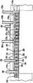
现参照附图,其中,相同的标号表示相同的元件,图1示出包括根据本发明一实施例的多气体喷射器的转动盘反应器。Referring now to the drawings, in which like numerals refer to like elements, Figure 1 shows a rotating disk reactor including a multi-gas injector according to an embodiment of the present invention.
如图1中示意地示出,该装置包括一用不锈钢壁105、一底板110、排气端口115以及一密封转动心轴125的转动的真空通孔馈通件制成的圆柱形反应腔室100,心轴顶上安装一带有基底晶片135的晶片载体130。晶片载体可围绕一与圆柱形腔室100同轴的轴线137(α)以预定转速(β)转动。As shown schematically in FIG. 1, the apparatus comprises a cylindrical reaction chamber made of
一加热基座145用一组加热元件140加热,加热元件通常由可折射的金属制成,例如但不限于钼、钨或铼等,或是诸如石墨那样的非金属,其可划分为多个加热区域。用于加热元件的金属可以根据所要实施的反应和特定反应器和化学气相沉积腔室所需要的加热特性进行选择。热屏蔽190有利地设置在加热元件140和加热基座145下方。或者,晶片载体130可通过辐射加热元件140直接地加热。A
加热元件140和反应器100通常通过一外部自动或手工的控制器193实施控制,而一可供选择的进入端口195有利地用来允许通向晶片135和晶片载体130,以便放置到反应器100内,可供选择地从第二腔室(未示出)放置。反应器的上述部件例如可以是用于由Veeco Instruments Inc.以商标名
一气体分配喷射器头150位于腔室100的上游端(如图1所示的朝向图顶部的一端)。气体分配喷射器头150包括这样的结构,其形成面向下游方向(如图1所示朝向图中底部的沿轴线137的方向)的一内表面155,并包括多个连接到第一前驱气体腔室或歧管170的第一气体入口160。A gas
各第一气体入口160包括一通道,该通道终止在通向喷射器内表面155的通道的下游端的一端口处。即,各第一气体通道与内表面155和第一前驱入口位置处的腔室100的内部连通。喷射器结构还形成多个连接到第二前驱气体腔室或歧管175的第二气体入口165。各第二气体入口也包括一通道,该通道终止在通向喷射器内表面155的通道的下游端的一端口处,以使第二气体入口165也与第二前驱入口位置处的腔室100的内部连通。第一前驱歧管170连接到第一前驱气体源180,而第二前驱歧管175连接到与第一前驱气体反应的第二前驱气体源185。Each
第一和第二前驱入口位置(入口160和165的下游端)沿水平方向(横向于下游方向和横向于轴线137,沿内表面155的方向)彼此间隔开,以便形成在喷射器内表面上延伸的一系列这样的部位。第一和第二前驱部位彼此散布。如以下将要描述的,入口部位可以设置成大致圆形的阵列,包括与轴线137同心的如此部位160、165的好几个环,随机地放置在内表面155上,或可以在其上放置成西洋跳棋棋盘、马赛克,或其它图形。The first and second precursor inlet locations (downstream ends of
喷射器结构还包括一多孔元件167,其在第一和第二前驱入口部位之间形成内表面155部分。用另一种方式来说,多孔元件延伸在第一前驱入口部位160和最近的第二前驱入口部位165之间。该结构还包括一与多孔元件167连通的载体气体歧管177。载体气体歧管连接到一载体气体源187,在大部分位于腔室100内的情形下,该载体气体最好与由源180和185供应的第一和第二前驱气体基本上不发生反应。正如在本发明中采用的,术语“基本上不反应”意味着载体气体不会与一个或两个前驱气体反应达到任何可感知的程度,而形成寄生加合物的固体沉积。此外,也可以形成寄生的气相加合物,它们可能不是反应性的且不会沉积,但仍然可能降低所需沉积过程的效率,并最好加以避免,但载体气体可以其它方式与前驱气体反应。离开喷射器的气体朝向反应腔室内的晶片载体在喷射器下游处释放。尽管本实施例显示为具有用来保持基底以便实施沉积过程的晶片载体,但也可构思不必使用晶片载体,而一基底可直接地放置在诸如卡盘那样的转动反应器表面上,无需一保持基底的晶片载体。这里所指的下游方向是朝向晶片载体的离喷射器的方向;它不必是相对于重力的任何特定定向。尽管这里所示的实施例显示出从腔室顶部朝向腔室底部下游方向,但喷射器也可放置在腔室侧上(以使下游方向是从腔室侧水平地朝向腔室中心的方向),或喷射器也可放置在腔室底部上(以使下游方向是从腔室底部向上地朝向腔室中心的方向)。再者,尽管排气端口115显示为在反应腔室的底部,但排气也可位于反应腔室的其它部分上。The injector structure also includes a porous member 167 that forms a portion of the
在操作中,一个或多个晶片135保持在晶片载体130内直接位于加热基座145上方。晶片载体130围绕轴线137以速率β在由电机120驱动的转动心轴125上转动。例如,β通常是约为500RPM或以上,但速率β可以变化。在其它实施例中,晶片载体不转动,例如,喷射器可以转动。电能转化为加热元件140中的热量并传递到加热基座145,其主要地通过辐射热量进行传递。加热基座145又加热晶片载体130和晶片135。In operation, one or
当晶片处于沉积反应所要求的温度时,第一前驱源180被致动而通过第一歧管170和第一前驱入口160馈送第一前驱气体,由此,从第一前驱入口排出腔室100内的大致下游处的第一载体气体流。同时,第二前驱源185被致动而通过歧管175和第二前驱入口165馈送第二前驱气体,由此,从第二前驱入口朝向基底或晶片130排出大致下游处的第二载体气体流。第一和第二前驱流不需精确地朝向下游和精确地平行于轴线137。在供应前驱气体的同时,载体气体供应187通过歧管177传递载体气体,以使载体气体通过多孔元件167并因此大致地流向下游,远离内表面155。When the wafer is at the temperature required for the deposition reaction, the
载体气体和第一和第二前驱气体通过下游朝向基底或晶片135。在如此通过过程中,诸气体彼此混和,以使前驱气体在基底上和基底附近处反应而形成一反应产物,该反应产物沉积在基底的暴露表面上。The carrier gas and the first and second precursor gases pass downstream towards the substrate or
在上述实施例中,同时提供两个前驱气体。然而,在其它实施例中,前驱其它顺序地和/或以交迭脉冲地供应。例如,在原子层外沿附生中,前驱气体的脉冲以交替顺序施加,以使一个载体气体的脉冲在另一气体脉冲开始之前终止。在称之为迁移增强的外沿附生过程中,不同载体气体的脉冲可以交替顺序但及时地彼此重叠地供应。在使用顺序前驱气体流的过程中,载体气体流可以与一个或多个前驱气体同时地供应。In the above embodiments, two precursor gases are provided at the same time. However, in other embodiments, the precursors are supplied sequentially and/or in overlapping pulses. For example, in epitaxy, pulses of precursor gases are applied in an alternating sequence such that a pulse of one carrier gas terminates before another gas pulse begins. In a process known as migration-enhanced epiphysis, pulses of different carrier gases can be supplied in alternating sequence but overlapping each other in time. In using sequential precursor gas flow, the carrier gas flow may be supplied simultaneously with one or more precursor gases.
载体气体阻止反应产物沉积在喷射器上。尽管本发明不受任何操作理论的限制,但可以认为载体气体就在内表面155附近阻止前驱气体的反向或向上游流动。此外,可以认为载体气体流降低第一和第二前驱气体在内表面附近的混和,并因此阻止反应产物形成在喷射器附近。The carrier gas prevents deposition of reaction products on the injector. While the invention is not limited by any theory of operation, it is believed that the carrier gas immediately adjacent the
前驱气体可以是适用于化学气相沉积过程的任何前驱气体。各种实施例中的前驱气体可包括任何气体、蒸气,或在反应器内参与基底处理的材料。具体来说,前驱气体可以是适用于处理基底表面的任何气体。例如,在所需沉积是诸如外沿附生层生长的半导体层的生长的情形中,前驱气体可以是多个化学品种的混和,并可包括惰性、非前驱气体的成分。任一前驱气体或两个前驱气体可包括诸如反应性前驱成分的气体和非反应性气体的一种组合。本发明转盘型反应器可适用的材料系的类型例如可包括III-V族的半导体,它们诸如但不限于GaAS、GaP、GaAs1-x、Px、Ga1-y、AlyAs、Ga1-ylnyAs、AlAs、AlN、InAs、InP、InGaP、InSb、GaN、InGaN等。此外,这些反应器也可应用于包括II-VI族化合物的其它系统,例如但不限于ZnSe、CdTe、HgCdTe、CdZnTe、CdSeTe等;诸如SiC、金刚石和SiGe之类的IV-IV族化合物;以及诸如YBCO、BaTiO、MgO2、ZrO、SiO2、ZnO和ZnSiO之类的氧化物;以及诸如铝、铜和钨之类的金属。此外,生成材料将具有宽范围的电子和光电子的应用,其包括但不限于发光二极管(LED)、激光、太阳能电池、光电阴极、高电子迁移率晶体管(HEMT)和金属半导体场效应晶体管(MESFET)。The precursor gas can be any precursor gas suitable for chemical vapor deposition processes. The precursor gas in various embodiments may include any gas, vapor, or material that participates in substrate processing within the reactor. In particular, the precursor gas can be any gas suitable for treating the surface of the substrate. For example, where the desired deposition is the growth of a semiconductor layer such as epitaxy growth, the precursor gas may be a mixture of chemical species and may include inert, non-precursor gas components. Either or both precursor gases may comprise a combination of gases such as reactive precursor components and non-reactive gases. The type of material system applicable to the rotating disk reactor of the present invention may include, for example, III-V semiconductors, such as but not limited to GaAS, GaP, GaAs1-x , Px , Ga1-y ,AlyAs , Ga1-y lnyAs, AlAs, AlN, InAs, InP, InGaP, InSb, GaN, InGaN, etc. In addition, these reactors are also applicable to other systems including Group II-VI compounds such as but not limited to ZnSe, CdTe, HgCdTe, CdZnTe, CdSeTe, etc.; Group IV-IV compounds such as SiC, Diamond and SiGe; and oxides such as YBCO, BaTiO,MgO2 , ZrO,SiO2 , ZnO, and ZnSiO; and metals such as aluminum, copper, and tungsten. Furthermore, the resulting materials will have a wide range of electronic and optoelectronic applications including, but not limited to, light-emitting diodes (LEDs), lasers, solar cells, photocathodes, high electron mobility transistors (HEMTs), and metal semiconductor field effect transistors (MESFETs). ).
载体气体可以是任何希望的载体气体,其不参与腔室内施加到基底上给予的前驱气体的沉积反应,诸如惰性气体或不参与反应的气体。The carrier gas may be any desired carrier gas that does not participate in the deposition reaction of the precursor gas applied to the substrate in the chamber, such as an inert gas or a non-reactive gas.
尽管图1的反应器显示为一垂直转动盘型反应器,但该反应器只是作为举例提供,应该理解到,本发明可用于诸如非转动盘反应器、侧向流反应器、转动喷射器反应器等的其它类型的反应器。此外,另外的前驱气体可通过一个或多个补充的气体源、气体腔室和气体入口供应到腔室。这里所述的图形和结构可因此连同一个或多个载体气体容易地延伸到三个、四个或更多个前驱。Although the reactor of Figure 1 is shown as a vertically rotating disk reactor, this reactor is provided by way of example only and it should be understood that the present invention can be used in reactions such as non-rotating disk reactors, side flow reactors, rotating injectors Other types of reactors such as reactors. Additionally, additional precursor gases may be supplied to the chamber through one or more supplemental gas sources, gas chambers, and gas inlets. The patterns and structures described here can thus be easily extended to three, four or more precursors along with one or more carrier gases.
喷射器头150和相关元件的机械结构显示在图2和3中。如图2-4所示的喷射器头150显示为坐落在反应器内,以使有时称之为“底部”表面的喷射器的下游表面(气体从其中喷射到反应腔室内)面向下,而有时称之为“顶”表面的喷射器的上游表面(气体源从其中供应气体到喷射器)面向上。The mechanical structure of
喷射器头150包括一密封板和一气体分配板210,其中,气体分配板210插入到密封板205内的一底切内,并通过多个螺钉(未示出)连接到密封板205。密封板有利地密封反应器100,同时将喷射器头150保持在反应器100内。气体分配板210具有用于水冷却的冷却通道215,其循着围绕气体分配板210的一路径(见图5中21C),这将在下面作详细描述。The
冷却水较佳地通过焊接到密封板205并用一O形环型的密封件225密封的入口220提供。类似的或其它的设计(例如,见图12、16)也可用于冷却水的输出流。Cooling water is preferably provided through
气体分配板210较佳地是借助于真空气密连接(例如,真空钎焊、扩散焊接、螺栓和密封结构等)而彼此连接的三个元件的组合。尤其是,气体分配板210通常包括一上游板240、一中间板235和一下游板230,它们的一个分区的实施例可见下面的图14-17。The
中间板元件235形成第一气体腔室245和前驱入口250。中间板元件235还较佳地具有用于冷却的水通道215。第一气体腔室245借助于一真空气密连接被连接到中间板235的上游板240而封闭。The
前驱通过一焊接到上游板240的管255提供给第一气体腔室245,并用一O形环密封件225密封。这些前驱通过导管(入口)250到达反应器内部空间。Precursor is supplied to the
一载体腔室260借助于真空气密连接方式连接到中间元件235。载体腔室260通过一多孔的下游板230在下面封闭。载体气体通过类似于位置255所示的一密封的载体入口管265供应到载体腔室260。多孔的下游板230包括表面(即,一屏)上的释放载体气体的多个小孔(例如,见图8B)。载体气体通过多孔的下游板230到达反应器内部空间。或者,一盖板(未示出)也可放置在下游板上方,如图12-16所示。A
第二组的前驱气体提供到三个独立区域内的气体分配喷射器。具体来说,分区域的前驱腔室270a-c由上游板240、带有O形环密封件的圆形连接器275a-b、以及密封板205形成。分区域的前驱腔室270a-c用来通过前驱导管280将前驱反应剂供应到反应器内,那里,各前驱腔室270a-c独立地对流量进行控制。圆形连接器275a-b和三个前驱入口管285a-c提供前驱入口的三个独立控制的区域,这将在下面图12-16的实施例中作进一步阐明。A second set of precursor gases is supplied to the gas distribution injectors in three separate zones. Specifically,
多孔下游板230的载体屏、前驱入口250和/或分成区域的前驱入口或导管280可以均匀地分布在喷射器内(下游)表面上,并可以非均匀的方式布置而沿径向变化密度,或如下面所述,可以均匀地分布但用浓度沿径向变化的前驱和载体供应。The carrier screen of the porous
如图4清晰地所示,一原位光学装置295开口设置一孔290,以代替一个前驱导管。As best shown in FIG. 4, an in
如图5清晰地所示,划分区域的前驱入口280沿着气体分配板210的底部(下游)表面以交替的图形点缀着前驱入口250。例如,诸如水、乙二醇等那样的冷却剂通过蜿蜒的(正弦)水通道215进入、通过和退出喷射器。还可提供用于光学视口(未示出)的孔290。这样,可提供晶片载体130(未示出)表面上均匀沉积所需要的恒定的前驱浓度。As best shown in FIG. 5 , the zoned
I.用载体入口图形散布多个前驱入口图形I. Interspersing Multiple Precursor Entry Patterns with Vector Entry Patterns
图6示出本发明一气体分配喷射器的实施例的截面图,其中,提供载体气体通过第三组的入口而不是一多孔板。应该理解到,尽管本气体分配喷射器的实施例被包括在一CVD转动盘反应器内,但本喷射器可用于任何多个其它环境中,包括不同的化学气相沉积、工业清洁环境等。Figure 6 shows a cross-sectional view of a gas distribution injector embodiment of the present invention wherein the carrier gas is provided through a third set of inlets instead of a perforated plate. It should be understood that although the embodiment of the gas distribution injector is included in a CVD rotating disk reactor, the injector may be used in any number of other environments, including various chemical vapor deposition, industrial cleaning environments, and the like.
转动盘反应器300的上游端包括一气体分配喷射器310,其也以简化形式显示在径向横截面内。第一前驱气体源330以控制的流量通过管子、歧管和阀网络350对喷射器下游表面上的一组第一前驱入口370提供第一前驱气体。一前驱气体390分配到反应器300内,在此情形中用来CVD处理一晶片。The upstream end of the
第二前驱气体源335通过第二管、歧管和阀网络355将第二前驱气体395提供到一组第二前驱入口375。第二前驱气体395也分配到喷射器下游表面上的反应器内。A second
为了防止前驱回射到喷射器入口上或入口内,该实施例中的喷射器310的下游表面上的前驱入口之间的空间365包括一组离散的载体入口360。一载体气体源320通过一管子、歧管和阀网络340提供一通过第二组入口360的载体气体380。载体气体380以用阀(未示出)手工设定的流量,通过控制载体气体源320,或通过控制管子、歧管和阀网络340,分配到反应器300内。To prevent precursors from back-reflecting onto or into the injector inlets, the
通过以均匀的或变化的径向密度、在喷射器310的全部内部下游表面上的前驱气体入口370和375之间的空间365内提供载体气体入口360,由此,载体气体流380提供到离各第一入口的第一前驱气体流390和离相邻的第二入口的最近的第二前驱气体流395之间。这里,载体气体380又在喷射器内部(下游)表面附近阻止第一前驱气体流390和第二前驱气体流395的混和。这样,载体气体流380有助于将反向喷射减到最小,并减小前驱材料在喷射器表面和喷射器入口内的积聚。By providing
图7示出本发明一实施例的气体分配喷射器的平面示意图,其从下游表面(从反应器内)观看。喷射器400提供一“马赛克”入口图形。喷射器400包括一前驱入口420和载体入口430定位在其上的下游(底部)表面410。在此实施例中,各个前驱入口被一非前驱入口围绕在所有侧面上,形成一“马赛克”瓷砖图形,其中,各个前驱入口完全地被载体入口或多孔载体屏包围。这样,前驱入口之间的空间设置有非前驱/载体入口,由此在喷射器处防止反向的喷射(和生成的残余前驱积聚)。尽管图7示出仅一个前驱,但应该理解到,在众多前驱入口的图形中可采用任何多个前驱。换句话说,一些前驱入口420可以是用于第一前驱气体的第一入口,而其它的前驱入口420可以是用于第二前驱气体的第二前驱入口。类似地,尽管图7示出前驱入口,但应该理解到,载体气体也可通过包括诸如图2所提供的一屏的多孔板喷射到反应腔室内。Figure 7 shows a schematic plan view of a gas distribution injector according to an embodiment of the invention, viewed from the downstream surface (from within the reactor).
图8A、8B和9示出本发明各种实施例的气体分配喷射器的示例的示意图,其从一反应器内的下游侧观看,气体分配喷射器在喷射器上使用各种结构的前驱入口和载体开口的组合。8A, 8B and 9 show schematic diagrams of examples of gas distribution injectors of various embodiments of the present invention, viewed from the downstream side within a reactor, using various configurations of precursor inlets on the injectors. and carrier opening combination.
在图8A中,一气体分配喷射器500包括一下游(底部)喷射器表面510、呈第一图形的第一前驱入口520、呈第二图形的第二前驱入口530,以及载体入口540。第一前驱和第二前驱入口以西洋跳棋棋盘图形散布载体入口,以便尽可能减小喷射器本身附近的第一和第二反应气体之间的互相作用,因此,减小反向喷射和在喷射器本身上积聚起前驱产物。In FIG. 8A , a
图8B示出一喷射器550,其具有位于喷射器本体560上的第一前驱入口570和第二前驱入口580的马赛克图形。散布在多个前驱入口之间空间内的是多孔板590内的多孔屏的开口,它们将载体气体喷射到前驱入口之间空间的反应腔室内,就如以上参照图1-4所讨论的。FIG. 8B shows an
类似地,图9示出另一实施例,其中,一气体分配喷射器600包括一喷射器内部下游(底部)表面610、呈第一图形的第一前驱入口620、呈第二图形的第二前驱入口630,以及载体入口640。一中心孔650包括一用于光学视口装置295或用于其它气体或反应器使用的材料通过的孔。第一前驱和第二前驱入口以马赛克图形散布载体入口,以便尽可能减小喷射器本身附近的第一和第二反应气体之间的互相作用,因此,减小反向喷射和在喷射器本身上积聚起前驱产物。Similarly, FIG. 9 shows another embodiment in which a
围绕中心孔650的喷射器中心区域可具有不同于其余突缘的入口布置,以便补偿转动盘反应器或中心载体气体入口的中心轴线。在此结构中,载体气体流不提供在就在孔650附近的那些第一和第二前驱气体入口之间。在其它实施例(未示出)中,载体气体流可在其它区域内省略,这样,载体气体流只提供在一些成对的而不是全部成对的邻近的第一和第二前驱入口之间。The central region of the injector around the
在上述实施例中,第一和第二前驱入口之间的空间用载体流气体净化。其结果,有利地减少前驱之间的预反应和前驱入口的阻塞。In the above embodiments, the space between the first and second precursor inlets is purged with carrier flow gas. As a result, pre-reaction between precursors and clogging of precursor inlets are advantageously reduced.
此外,前驱气体入口可以彼此分离开相当的距离。仅用来举例而已,前驱气体入口可以每平方英寸10入口量级(1.55入口/cm2)的入口密度设置。不必为了将反向喷射减到最小而紧密地挤满前驱入口。因此,这些实施例提供一更加可靠和可适于制造的设计,且为原位光学视口或其它气体通过提供空间。然而,也可使用入口之间的其它的距离。Furthermore, the precursor gas inlets may be separated from each other by a considerable distance. By way of example only, the precursor gas inlets may be provided at an inlet density on the order of 10 inlets per square inch (1.55 inlets/cm2 ). It is not necessary to tightly crowd the precursor inlets in order to minimize back injection. Thus, these embodiments provide a more reliable and manufacturable design, and provide room for in situ optical viewports or other gas passages. However, other distances between the inlets may also be used.
气体入口可以同心地或相对于喷射器中心轴线径向地放置。前驱相对于载体气体的浓度可以沿径向变化。替代地或添加地,喷射器表面上的前驱和载体入口的密度可沿径向变化。The gas inlets may be placed concentrically or radially relative to the central axis of the injector. The concentration of the precursor relative to the carrier gas can vary radially. Alternatively or additionally, the density of precursor and carrier inlets on the injector surface may vary radially.
II.散布的载体/前驱入口的浓度分区II. Concentration Partitioning of Dispersed Carrier/Precursor Inlets
在一实施例中,对前驱提供多区域的喷射,以补偿诸如非均匀的前驱分解和非均匀的晶片载体温度之类的效应。较佳地,提供三个径向区域,但其它结构也纳入本发明的范围之内。In one embodiment, multi-zone injection of the precursor is provided to compensate for effects such as non-uniform precursor decomposition and non-uniform wafer carrier temperature. Preferably, three radial regions are provided, but other configurations are within the scope of the invention.
通过在不同的喷射点以变化的浓度水平将前驱气体喷射到反应腔室内,可促进均匀的材料部署。换句话说,前驱浓度可以作成前驱喷射坐标的函数。因此,另外可拥有一较高或较低前驱浓度的反应腔室的区域可以较低或较高的前驱浓度补偿予以“充实”。Uniform material deployment is facilitated by injecting precursor gases into the reaction chamber at varying concentration levels at different injection points. In other words, the precursor concentration can be made a function of the precursor injection coordinates. Thus, regions of the reaction chamber that would otherwise have a higher or lower precursor concentration can be "filled" with lower or higher precursor concentration compensation.
可实施上述方案的一种方式是将气体分配喷射器分成多个同心的区域。各个同心区域包含多个入口,它们将前驱气体喷射到一反应腔室内。各区域内的前驱气体浓度例如通过各自径向区域不同地控制前驱浓度而独立地进行控制。或者,可借助于各自区域不同地控制前驱浓度,可促进具有已知非均匀图形的功能性地控制材料沉积。在一替代的实施例中,前驱入口相对于载体入口的浓度可以变化,或总体前驱入口的浓度可以变化以达到相同的效果。One way the above can be implemented is by dividing the gas distribution injector into multiple concentric regions. Each concentric region contains multiple inlets that inject precursor gases into a reaction chamber. The concentration of the precursor gas in each region is independently controlled, for example, by controlling the concentration of the precursor differently for each radial region. Alternatively, a functionally controlled deposition of material with a known non-uniform pattern can be facilitated by virtue of the respective region being able to control the concentration of the precursors differently. In an alternative embodiment, the concentration of the precursor inlet relative to the carrier inlet may be varied, or the concentration of the overall precursor inlet may be varied to achieve the same effect.
图10示出一根据本发明的实施例的空间分布的喷射系统700。如图10所示,喷射器700的下游(底部)表面710形成多个入口720。表面710组织成两个区域725和730。在图10所示的特定实施例中,表面710呈圆形,且区域725和730是同心圆。原则上,表面710可以是任何形状,且不需是平面的(例如,可以是球体、半球、凹陷的或凸出的)。类似地,区域725和730可以是任何形状,且不需是圆形或同心的。FIG. 10 shows a spatially distributed
各个区域725和730的入口720用起源于独立容器的两个前驱气体予以供应:用来自于容器735和740的前驱气体供应区域725内的入口;用来自于容器745和750的前驱气体供应区域730内的入口。容器735和745各包含第一前驱气体。然而,包含在容器735内的前驱气体处于一种浓度,而容器745内的该前驱气体处于不同的浓度水平。类似地,容器740和750各包含第二前驱气体。还是如此,包含在容器740内的前驱气体处于一种浓度,而容器750内的该前驱气体处于不同的浓度水平。因此,各区域725和730用第一和第二前驱气体供应,但各区域喷射不同浓度水平的这些前驱。各区域浓度的变化可用来补偿以另外方式发生的反应腔室区域内浓度的波动。The
总而言之,入口系统700包括一形成多个入口720的入口表面710。入口720组织成多个区域725和730。对于各区域725和730,对于各个前驱气体存在着一个容器,以便将前驱气体喷射到附连的反应腔室内。该方案的结果是,各区域725和730可喷射不同浓度的前驱气体。当然,也可作出其它的变量来变化各自的区域(例如,可变化各自区域的前驱的压力、温度,或离子电荷)。尽管图10所示的喷射系统700包含两个区域725和730,各区域用两个前驱气体供应,喷射系统700可包括任何数量的区域,各个区域可用任何数量的前驱气体供应。所有供应到一给定区域的前驱气体可处于一单一浓度水平,或可处于变化的浓度水平。各自区域的各前驱可独立地具有其浓度变化,这对于补偿从一种前驱到另一前驱的分解速率的变化是重要的。喷射器700的下游表面710上的入口可包括载体入口,其呈离散载体入口的形式,或如上所述的多孔元件的形式,一组或多组前驱入口用于一个或多个前驱。In summary,
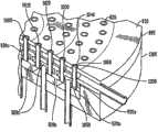
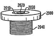
图11是喷射器800的立体图,其可用于图10的空间分布的喷射系统700内。如图11所示,喷射器800的面向下游(底部)的内部表面810形成多个入口820。喷射器800还拥有一冷却剂入口导管830和冷却剂出口导管835,以便如下所述地通过一冷却腔室传递一冷却流体(诸如水)。图11-16示出一具有朝向结构顶部的下游方向的气体分配喷射器,即,与图1-4的喷射器的定向相反的方向。入口820分成三个同心的区域840、850和860。FIG. 11 is a perspective view of an
图12示出图11所示喷射器800的剖视的立体图。各个入口820连接到由喷射器800的本体形成的两个圆柱形腔室900和910之一上。腔室900分成为环形的分腔室920a、920b和920c,由此,腔室910分成为环形的分腔室930a、930b和930c。各个区域840、850和860与腔室900的一个分腔室920a-c和腔室910的一个分腔室930a-c相连。例如,分腔室920a和930a对应于区域860。因此,区域860内的入口连接到分腔室920a和930a。类似地,区域850内的入口连接到分腔室920c和930c。FIG. 12 shows a cut-away perspective view of
分腔室920a-c和930a-c被称之为分腔室,而不是称之为单独的“腔室”,因为它们通过多个壁将单一腔室900或910划分为许多个“分腔室”。喷射器800的该方面在下面予以详细地说明。如图12所示,各个分腔室920a-c和930a-c拥有一分别连接到一导管940a-c和950a-c的孔。该孔和导管的组合允许前驱气体喷射到分腔室920a-c和930a-c内。因此,各个分腔室920a-c和930a-c可以用其自己的前驱气体源供应。The sub-chambers 920a-c and 930a-c are referred to as sub-chambers rather than individual "chambers" because they divide a
一圆柱形冷却腔室960位于反应腔室(未示出)和第一和第二腔室900和910之间。例如,诸如水那样的冷却剂循环通过冷却腔室960。入口820在途中通过冷却腔室960到达反应腔室。因此,前驱气体通过冷却腔室960(不与其连通),由此,被冷却到低于阈值点的温度以便于沉积反应。一诸如水那样的冷却剂进入和退出冷却腔室960,以便通过水入口970和水出口980循环。A
图13示出图12所示横截面部分的放大视图。如图13清晰地所示,各入口820具有一同轴的喷射导管,其由围绕第二导管定位的第一导管形成。例如,喷射导管1040包括一内导管1050。内导管1050提供一通道,分腔室920a内的前驱气体可通过该通道移动到反应腔室。围绕内导管1050的是一外导管1060。外导管1060提供一通道,分腔室930a内的前驱气体可通过该通道移动到反应腔室。内和外导管1050和1060最好是同心的。因此,如图17所示,在下游表面810处的各个入口820包括同轴的导管,其包括由同轴壁1390分成的内导管开口1370和外导管开口1380。同轴的导管1030将另一入口820连接到分腔室930a和920a,同轴的导管1020和1010将入口连接到分腔室930b和920b,同轴的导管1000将另一入口连接到分腔室930c和920c。内和外导管的横截面面积可以相等或不相等。这些面积之比可以随区域而变,或甚至在一区域内变化。同轴导管的配置允许前驱气体从其对应的分腔室运输到反应腔室,而在前驱之间没有横向连通。此外,同心导管可将形成在表面810上的沉积减到最少。尽管从各个导管退出的两个前驱气体彼此混和,但可以认为,从外导管1000退出的前驱气体流的最外部分在离内下游喷射器表面810下游处的有限距离内保持未被混和。朝向表面810的任何反向喷射或回流将主要地由该最外部分的气体组成。FIG. 13 shows an enlarged view of the cross-sectional portion shown in FIG. 12 . As best shown in Figure 13, each
图11-13所示的特定的喷射器不包括如上所述的提供给一分离的内载体气体供应。然而,如下所述,可提供这样一载体气体供应,其具有在出口820之间形成表面810部分的一多孔元件或具有离散的载体气体出口,以便进一步将反向喷射减到最小。使用同轴的导管可简化喷射器的结构,其可减少所需密封量。此外,使用同轴配置允许前驱材料有更加均匀的分布。当然,图10-13的分区结构可用于如图1-4所示的分离的第一和第二前驱入口。尤其是如该替代方案中所示,第一前驱气体入口连接到分腔室920a-920c,而第二前驱气体入口连接到分腔室930a-930c。类似地,如上所述,同轴导管可用来以交替或其它图形分散一个或多个前驱气体通过内导管,同时分散一载体气体通过各同轴导管的外导管。The particular injector shown in Figures 11-13 does not include a separate internal carrier gas supply as described above. However, as described below, a carrier gas supply may be provided with a porous element forming part of
图14至16是一组板的剖视立体图,图10的喷射器700用该板进行构造。14-16 are cut-away perspective views of a set of plates with which the
在图14中,示出一上游板1100。该上游板1100较佳地是圆形,并包含三个凹陷区域1110、1120和1130。同心圆壁1140和1150分离开凹陷区域1110、1120和1130。凹陷区域1110、1120和1130联合起来组成如图12所示的第一腔室900。凹陷区域1110组成分腔室920c。类似地,凹陷区域1120和1130分别组成分腔室920b就920a。根据图14的理解,可见腔室900形状大致呈圆柱形,并分成一组三个同心圆柱形的分腔室1110、1120和1130。第一组的导管940a-c分别从凹陷区域1130、1120和1110向上游(朝向反应器外的气体源)延伸。导管940a、940b和940c用作通道,前驱气体可通过该通道喷射到由凹陷区域1110、1120和1130形成的各种分腔室内。第二组的导管950a、950b和950c延伸通过上游板1100。第二组导管在近似等于同心圆壁1140和1150高度的高度上从上游板1100向下游(朝向反应器)突出。每一区域可有一个以上导管,导管数量可随区域不同而变化。In Fig. 14, an
图15示出堆叠在上游板1100顶上的中间板1200。中间板1200搁置在由上游板1100形成的圆柱形壁1140和1150顶上。与上游板1100相同,中间板1200也包含凹陷区域1210、1220和1230。凹陷区域1210、1220和1230被圆壁1240和1250分离。凹陷区域1210、1220和1230联合起来组成第二腔室910,并分别单独地组成分腔室930a、930b和930c。根据对图15的理解可以得知,可见第一和第二圆柱形腔室900和910彼此堆叠在顶上,并享有一公共面(中间板1200)和一公共的纵向轴线。中间板1200连接各个第二组的导管950a、950b和950c,它们从上游板1100朝向下游(朝向反应腔室)突出。因此,第二组导管950a、950b和950c用作通道,前驱气体可通过该通道喷射到由凹陷区域1210、1220和1230形成的各种分腔室内。FIG. 15 shows the
此外,每一区域可有多个导管,且导管数量可随区域不同而变化。中间板1200也包含多个喷射导管1260,它们从板1200朝向下游(朝向反应腔室)突出,延伸超过圆形壁1240和1250的高度。喷射导管1260的全高在图16中未示出;为了图示的清晰起见,已移去这些导管的部分。Additionally, there can be multiple conduits per zone, and the number of conduits can vary from zone to zone. The
图16示出堆叠在中间板1200顶上的下游板1300。下游板1300搁置在由中间板1200形成的圆形壁1240和1250顶上。下游板形成图12所示的冷却腔室960的下游部分。根据对图16的理解可以得知,可见圆柱形冷却腔室960和第二圆柱形腔室910彼此堆叠在顶上,并享有一公共面(下游板1300)和一公共的纵向轴线。FIG. 16 shows the
如图12和13清晰地所示,冷却腔室960位于下游板1300和盖板805之间,盖板805形成喷射器1100的内部或面向下游的表面810。在此实施例中,导管1320通过冷却腔室,但不与冷却腔室连通。如图16所示,下游板1300的侧部提供用于冷却腔室960的孔1330和1340的入口和出口。入口和出口孔1330和1340连接入口和出口的导管830和835。因此,孔1330和1340和导管830和835合作到冷却腔室,冷却剂流体可通过冷却腔室循环通过喷射器。用来循环冷却剂的腔室可以是一如图16所示的敞开腔室,或可以如图5所示地遵循其它二维或三维几何形。As best shown in FIGS. 12 and 13 , the cooling
下游板1300包含多个喷射导管1320,它们从板1300朝向反应腔室向下游突出,并延伸到与由中间板1200连接的喷射导管1260相同的高度。连接到下游板1300的导管1320围绕连接到中间板的导管1260形成,因此,形成参照图13和17所描述的同轴导管结构。如图11、12和13清晰地所示,一盖板805躺在下游板1300上并形成如图11所示的喷射表面810,还形成也示于图11中的多个入口820。此外,盖板805密封关闭的喷射器。在入口820处,盖板805密封到喷射导管1320。图17详细地所示的一同轴入口的实施例示出了盖板805的喷射(下游)表面810上的同轴入口820。一外同轴壁1360和一内同轴壁1390形成了外同轴入口1380。外同轴入口1380部分地或完全地包围一由内同轴壁1390形成的内同轴入口1370。外同轴入口1380和内同轴入口1370可分配第一和第二前驱气体,或者,内同轴入口1370可分配一前驱气体,而外同轴入口1380分配一包围前驱气体的载体气体罩。相反,由内同轴入口1370承载载体气体也是可能。The
III.具有分区域的入口和多前驱入口的气体分配喷射器(同轴或双腔)III. Gas Distribution Injectors (Coaxial or Dual Chamber) with Zoned Inlets and Multiple Precursor Inlets
图18示出本发明的一实施例,其中,通过散布在载体入口均匀范围内的入口提供多个前驱。下游(内部)的喷射器表面1400分成为多个区域1410、1420和1430。在各个区域内,提供第一前驱入口1440、第二前驱入口1450和载体入口1460的西洋跳棋棋盘图形,以便将前驱均匀地分配到反应器内的晶片载体,不造成材料反向喷射到喷射器本身上。Figure 18 shows an embodiment of the invention in which multiple precursors are provided by inlets dispersed over a uniform range of carrier inlets. The downstream (inner)
类似地,在图19中,提供图18结构的一变体,其中,第一前驱入口和第二前驱入口组合成双腔入口。具体来说,下游内喷射器表面1500分成为多个区域1510、1520和1530。在各个区域内,提供双腔前驱入口1540和载体入口1550的西洋跳棋棋盘图形,以便将前驱均匀地分配到反应器内的晶片载体,不造成材料反向喷射到喷射器本身上。Similarly, in Figure 19, a variation of the structure of Figure 18 is provided in which the first precursor inlet and the second precursor inlet are combined into a dual chamber inlet. Specifically, downstream
如图20所示,各双腔前驱入口1540分成较小的导管(入口)1560和1565,它们承载第一前驱1570和第二前驱1575,且它们被一腔壁1580划分而分离第一前驱和第二前驱,直到它们进入反应器腔室。双腔前驱入口1540可以被如图13-17详细所示的同轴入口1590代替。在图18-19的实施例中,载体入口可以有利地用如图2所示的载体多孔板代替。As shown in FIG. 20, each dual
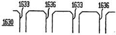
图21A-G提供本发明入口的一些实施例的横截面图(为清晰起见,不包括载体多孔板)。如图所示,诸入口向下游地通向反应腔室内。图21A示出包括以简单西洋跳棋棋盘图形散布的载体入口1603和前驱入口1606的横截面1600。在图21B中,横截面1610示出带有双腔前驱入口1616(图20所示类型)以西洋跳棋棋盘图形散布的载体入口1613和冷却通道横截面1618。在图21C中,横截面1620示出带有载体入口1623以西洋跳棋棋盘图形散布的同轴前驱入口1626(图17所示类型)和冷却通道横截面1628。在图21B中,横截面1610示出双腔前驱入口1616,其包括一线性阻挡体1615以将第一前驱导管与第二前驱导管密封。类似地,在图21C中,同轴前驱入口1626部分地由一径向阻挡体1625,其将第一前驱导管与周围的第二前驱导管密封。Figures 21A-G provide cross-sectional views of some embodiments of inlets of the present invention (carrier perforated plates are not included for clarity). As shown, the inlets open downstream into the reaction chamber. Figure 21A shows a
尽管图21A-C分别示出横截面1600、1610和1620,各近似地示出入口边缘处的法向角,但也可通过提供入口和喷射器内部下游表面之间的倾斜边界进一步减小喷射。因此,在图21D中,横截面1630示出以简单西洋跳棋棋盘图形散布并倾斜而进一步减小喷射的前驱入口1636和载体入口1633。在图21E中,横截面1640类似于横截面1630,在此实例中,例外地是,仅前驱入口1646倾斜,而载体入口1643保持法向。在图21F中,横截面1650示出带有线性阻挡体1655的双腔前驱入口1656,它们与载体入口1653一起以西洋跳棋棋盘图形散布,其中,双腔入口1656和载体入口1653以大致45度角倾斜,以进一步将粘度减到最小。最后,在图21G中,横截面1660示出带有径向阻挡体1665的同轴前驱入口1666,其与载体入口1663一起以西洋跳棋棋盘图形散布。冷却通道横截面1668不与同轴前驱入口1666或载体入口1663气体地连通,但与入口1666和1663热力上连通,以便在操作过程中,减缓喷射器的温度。Although Figures 21A-C show cross-sections 1600, 1610, and 1620, respectively, each approximately showing the normal angle at the inlet edge, jetting can be further reduced by providing a sloped boundary between the inlet and the injector interior downstream surface. Thus, in FIG. 21D ,
在图21F和21G中,分别示出横截面1650和1660,阻挡体1655和径向阻挡体1665较佳地倾斜于入口和反应器腔室前的稍许在边界前的端部,以进一步将粘度和喷射减到最小,但阻挡体1655或1665也可终止在边界或超过边界,视对于特定喷射器的个别结构而定。In Figures 21F and 21G, showing cross-sections 1650 and 1660, respectively, barrier 1655 and radial barrier 1665 are preferably sloped towards the inlet and slightly forward of the boundary in front of the reactor chamber to further reduce the viscosity and jets are minimized, but barriers 1655 or 1665 may also terminate at the boundary or beyond the boundary, depending on the individual configuration for a particular injector.
IV.具有允许定制端口和孔规格的可更换的入口元件的喷射器IV. Injectors with Replaceable Inlet Elements Allowing Custom Port and Orifice Specifications
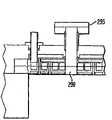
图22是本发明一气体分配喷射器的另一实施例的简化局部截面图。用来放置在沉积反应器内的喷射器1700由一上游板1710、一中间板1720和一下游板1730形成,它们通过诸如真空钎焊、焊接或螺栓和密封件的结构之类的密封过程连接在一起。喷射器通常连接到反应器腔室的密封板1701上(见图2)。图23是本发明一气体分配喷射器的实施例的分解立体图,其使用多个气体分配板并包括用来将气体连通到反应器腔室的通气螺钉。例如,气体分配喷射器位于反应器密封板(未示出)下方,其用该密封板形成第一反应剂气体歧管(见图2),并较佳地位于一反应器腔室(未示出,见图1)内,以使一晶片载体(未示出,见图1)中心地位于气体分配喷射器下方。Figure 22 is a simplified partial cross-sectional view of another embodiment of a gas distribution injector of the present invention. The
如图22所示,上游板1710包括一上游表面1740和一下游表面1745。形成第一反应剂气体歧管1702的空间通常位于上游板1710的上游表面1740和密封板1701之间(例如,见图2、270a-c)。较佳地,一个或多个气体入口元件与上游板1710的上游表面1740齐平,在此情形中,通气螺钉1760与一中心地位于各个通气螺钉1760内的气体入口1770齐平。通气螺钉1760通过上游板1710的上游表面1740内的一个或多个螺钉孔1765,固定到上游板1710的上游表面1740,其中,螺钉孔1765与第一反应剂气体通道对齐。As shown in FIG. 22 ,
在图23中,立体图地可见图22中描述的上游板1710、中间板1720和下游板1730。在图23所示的上游板1710中,多个通气螺钉1760固定在通气螺钉孔1875内,以对从第一气体歧管进入气体分配喷射器内的第一反应剂气体提供一入口。用于光学视口或气体源连通到气体分配喷射器内的喷射器密封端口1870位于顶表面1740上。冷却剂贯通开口1895允许冷却剂进入和退出管线通过上游板1710的结构。最后,螺栓孔1890允许上游板密封到其它气体喷射器板和反应器的密封板上。In FIG. 23 , the
图24A是图22所示气体分配喷射器实施例的上游板的详细的立体图。上游板1710显示为其顶表面1740可见,且其中还可见多个通气螺钉孔1875。此外,一组冷却剂贯通开口1895允许冷却剂导管进入和退出通过上游板到冷却通道所定位的中间板(未示出)。提供多个密封端口1870,使气体和/或光学视口连通到气体分配喷射器内或通过气体分配喷射器。尤其是,提供第二反应气体密封端口1872,使第二反应气体通过上游板1710连通到一区域,该区域介于上游板的下游表面1745和中间板(未示出)的上游表面之间,它们形成第二反应剂气体歧管1790。24A is a detailed perspective view of the upstream plate of the embodiment of the gas distribution injector shown in FIG. 22. FIG.
图24B是图22所示气体分配喷射器实施例的上游板的仰视图,详细地示出上游板1710的的下游表面1745。如上所述,上游板1710包括多个冷却剂贯通开口1895、用来通过第一反应气体的气体通气螺钉孔1875、用来密封端口1870的通孔,以及用来将上游、中间和下游板连接在一起的螺栓孔1890。24B is a bottom view of the upstream plate of the embodiment of the gas distribution injector shown in FIG. 22 showing the
第二反应气体密封端口包括第二反应气体密封端口出口1873,其使第二反应气体连通到第二反应气体歧管1790的本体。可供选择地,在第二反应气体歧管1790内,一径向阻挡体1878形成第二反应气体歧管1790的两个区域:一外环1878,第二反应气体最初通过第二反应气体密封端口出口1873连通到该外环1878,以及一内歧管区域1883,其中,第二反应气体如本文所描述地连通到中间板1720内。外环1878和内歧管区域1883通过多个孔1882连通,这多个孔1882用来平衡第二反应气体歧管1790的内歧管区域1883内的第二反应气体的气体压力。The second reactant gas seal port includes a second reactant gas
返回到图22,中间板1720包括一上游表面1750和一下游表面1755。上游板1710和中间板1720可连接在一起,例如,通过真空焊接或在上游板1710和中间板1720之间的接触点处的螺栓和密封结构实现连接。上游板1710的下游表面1745的一部分连同中间板1720的上游表面1750一起形成用来将第二反应气体引入到反应腔室内的第二反应气体歧管1790。一气体入口1810(可供选择地通过一个或多个固定在一个或多个通气螺钉孔1805内的通气螺钉1800)形成在中间板1720的上游表面1750内。Returning to FIG. 22 , the
一冷却通道1840形成在中间板1720的上游表面1750内(例如,见图5和25A-C)。冷却通道1840的上游端密封,并与气体分配喷射器1700的其它部件分离,尤其是,通过一冷却通道盖板1850与中间板1720的上游表面1750密封,冷却通道盖板1850较佳地通过真空焊接到中间板1720的上游表面1750,以在中间板1720的上游表面1750上形成一毗邻的表面,并因此形成毗邻的水冷却通道1840,如图25A-C中详细地所述。A
形成在中间板1720的下游表面1755内的是一个或多个载体气体歧管1830,它们接受最好是非反应的载体气体以便分配到反应器内。还有形成在中间板1720下游表面1755内的是通气螺钉孔1795,它们用来固定包括第一气体出口1785于其中的第一气体出口的通气螺钉1780。第一气体出口的通气螺钉1780和第一气体出口1785用作为第一气体的通道1775的终点,因此,允许第一反应气体从第一气体歧管传送到反应腔室。还形成在中间板1720的下游表面1755内的是第二气体出口1820,其用作为第二气体的通道1815的终点,因此,允许第二反应气体从第二气体歧管1790传送到反应腔室。或者,第二气体出口1820可由类似于用于第一气体出口1785的结构的通气螺钉结构形成。Formed in the
如图23中分解立体图中所示和根据不同立体图所描述的,中间板1720包括一焊接的上游表面板1840和一下游表面1755,并连接到冷却剂入口和出口管1880,它们将诸如水的冷却剂提供到位于如这里所述的中间板1720内的冷却通道。气体入口1810位于中间板1720的上游表面板1840内,一些气体入口1810连接到上游板1720内的第一气体入口,而一些气体入口1810直接从形成在上游板1745的下游表面和中间板1720的上游表面1840之间的第二气体歧管中接受第二气体。螺栓孔1900允许中间板密封到喷射器的其它板上。As shown in the exploded perspective view of FIG. 23 and described according to different perspective views, the
图25是图22所示气体分配喷射器实施例的中间板的详细的立体图。中间板1720的上游表面1750用来形成第二反应气体歧管1790的下游端,包括用于第二反应气体(和用于第一气体通道,该通道通过但与第二气体分配歧管不连通)的气体入口1800。中间板1720还包括用于气体分配喷射器的冷却通道1840。中间板还包括:螺栓孔1900,用来将上游、中间和下游板固定在一起;以及密封端口管线通孔1910,用于光学视口或连通气体分配系统内的气体。25 is a detailed perspective view of the intermediate plate of the embodiment of the gas distribution injector shown in FIG. 22. FIG. The
图26A是图22所示气体分配喷射器实施例的中间板的立体图,其显示为在将冷却通道盖板1850焊接到上游表面上之前(见图26B),以便更清晰地显示位于其中的冷却通道1840。位于中间板1720的上游表面1750上的反应气体入口1820用实线示出,而位于下游表面1755上的反应气体入口1820的出口用虚线示出。图26B是图22所示气体分配喷射器实施例的中间板的立体图,其显示为在将冷却通道盖板1850焊接到上游表面上之后。冷却剂导管1930提供诸如水那样的冷却剂进和出,进入到如图26A中所示的冷却通道1840内。26A is a perspective view of the middle plate of the embodiment of the gas distribution injector shown in FIG. 22, shown prior to welding the cooling
再返回到图22,下游板1730可以是一薄板,其包括布置在其中的单一的或多个能透过或打孔的区域1735。下游板1730通过诸如真空焊接或螺栓和密封结构那样的工艺连接到中间板1720的下游表面1755。下游板1730的打孔区域1735至少与中间板1720的下游表面1755内的载体气体歧管1830相一致,以允许载体气体分配到位于下游板1730的下游的反应腔室内。Returning again to FIG. 22, the
在下游板1730处,第一反应气体通道1775终止在位于下游板1730上的气体出口1785,其单独地或位于诸如一气体出口通气螺钉1780那样可移去的装置内。可供选择地是,气体出口通气螺钉1780可有利地固定到下游板1730,以将下游板1730固定在气体出口通气螺钉1780和中间板1720的下游表面1755之间。第二气体通道1815通过第二气体出口1820终止,第二气体出口1820较佳地完全通过下游板1730连通,以便将第二反应气体分配到反应腔室。At the
如从图23中的另一立体图中所示,下游板1730包括多个孔1820,通过这些孔第一气体出口和第二气体出口从中间板1720的下游表面1755与反应腔室连通。最后,多个气体出口通气螺钉1780固定到中间板1720的底部1755内的出口通气螺钉孔(见图22),以便进一步将下游板1730固定到气体出口通气螺钉1780和中间板1720之间。气体出口通气螺钉用于如图22所示的第一反应气体出口,但可供选择地也可用于第二反应气体出口。最后,下游板内的螺栓孔1940有利地与中间板的螺栓孔1900和上游板的螺栓孔1890对齐,以便用螺栓连接在一起和密封,或用其它方法连接上游、中间和下游板。在下游板上,如图27所示,较佳地是一载体气体屏,用来将载体气体散布在反应气体出口之间的区域内。As shown from another perspective view in FIG. 23 , the
图27是图22所示气体分配喷射器实施例的下游板的视图,该图从反应器内部观察(从下游方向)。下游板1730包括一载体气体屏1735,该屏可以是多孔的或可渗透一载体气体,,该载体气体可通过其间。载体气体屏1735显示为一单一连续的区域,但也可设置在位于垂直地邻近于载体气体歧管1830的一离散的多个区域内,显示为离散的气体入口,显示为用于各多个同轴的内反应剂入口的多个外同轴的入口,或其它的结构。对第一气体通气孔1795和通过下游板1730的第二气体出口1820设置多个孔。下游板1730的外区域1945最好是实心的不构成一屏。设置螺栓孔1940以将上游、中间和下游板彼此固定和固定到反应器。Figure 27 is a view of the downstream plate of the embodiment of the gas distribution injector shown in Figure 22, as viewed from inside the reactor (from the downstream direction).
图28是本发明的一气体分配喷射器的实施例的截面图,其包括放置在反应剂气体入口通道内以便形成一压差的多孔材料。另外类似于图22的实施例,图28还示出将渗透材料1960引入第一气体通道1775内,以控制气体压力,以及使用用于第二气体出口1975的第二气体出口通气螺钉1970,就如上述的第一气体出口通气螺钉1780。Figure 28 is a cross-sectional view of an embodiment of a gas distribution injector of the present invention that includes porous material positioned within the reactant gas inlet passage to create a pressure differential. Also similar to the embodiment of FIG. 22 , FIG. 28 also shows introduction of
渗透材料1960例如可以是一碳过滤器或其它不与通过其间的第一反应气体反应的渗透材料,渗透材料1960用来在第一气体入口1770和第一气体出口1785之间形成压差。或者,渗透材料也可用于第二气体通道。The
此外,代替渗透材料或添加到渗透材料,可分别变化通气螺钉1760和1785或其它可移去的气体入口装置的内直径来形成一相似的压差,例如,通过增加或减小第一气体入口通气螺钉1760内的第一气体入口1770的孔大小,和/或增加或减小第一气体出口通气螺钉1780内的气体出口1785的孔大小。Furthermore, instead of or in addition to the permeable material, the inner diameters of the vent screws 1760 and 1785 or other removable gas inlet devices can be varied, respectively, to create a similar pressure differential, for example, by increasing or decreasing the first gas inlet The hole size of the
再者,图28中使用了气体出口通气螺钉来分配第一反应剂气体和第二反应剂气体。尤其是,对于第二气体出口1975设置第二气体出口通气螺钉1970,就如对于第一气体出口1785设置上述的第一气体出口通气螺钉1780。通过变化通气螺钉的结构,包括通气螺钉的深度、通气螺钉头超出下游板的表面多远,或中心地位于对应通气螺钉内的气体入口和气体出口的直径,通气螺钉内气体出口孔大小和维度因此可有利地根据反应器和气体喷射器结构进行定制,无需更换气体喷射器的其它结构部件。Again, a gas outlet vent screw is used in FIG. 28 to distribute the first reagent gas and the second reagent gas. In particular, a second gas
图29是使用同轴反应剂气体入口和通气螺钉的本发明气体分配喷射器实施例的内气体分配表面的截面图。一同轴的气体出口通气螺钉2000连接到下游板1730和中间板1720内的同轴反应气体通道2005。同轴反应气体通道2005包括一用于第一气体的外通道2010和一用于第二气体的内通道2020,其中,内和外通道被一内径向壁2030分离。如上所述,中间板1720包括一载体气体歧管1830,其从一载体气体通道1980中接受载体气体,而且其通过下游板1730内的一多孔屏1735将气体分配出气体分配喷射器外。图中还示出中间板1720内的冷却通道1990的截面图。Figure 29 is a cross-sectional view of the inner gas distribution surface of an embodiment of a gas distribution injector of the present invention using a coaxial reactant gas inlet and vent screw. A coaxial gas
图30是使用一非同轴双腔反应剂气体入口和通气螺钉以及一补充反应剂气体入口的本发明气体分配喷射器实施例的内气体分配表面的截面图。一双腔气体出口通气螺钉2040连接到下游板1730和中间板1720内的双腔反应气体通道2045。双腔反应气体通道2045包括一用于第一气体的左通道2050和一用于第二气体的右通道2060,其中,右和左通道被一中心壁2070分离。如补充的反应气体出口2090所示,其显示为连接到一不使用同轴双腔或通气螺钉设计的补充的反应气体通道2080,这里所述的各种入口和出口设计包括图21A-G所示的那些设计,以及不同测量计、入口直径和出口形状的通气螺钉可组合在同一个气体分配喷射器中,以允许各种的气体分配结构。代替载体屏1735,例如,第一和第二同轴入口可提供来分配第一和第二前驱气体,其中,第一和第二前驱通过各个同轴入口的内同轴通道进行分配,而一载体气体通过各同轴入口的外同轴通道进行分配。Figure 30 is a cross-sectional view of the inner gas distribution surface of an embodiment of a gas distribution injector of the present invention utilizing a non-coaxial dual chamber reactant gas inlet and vent screw and a supplemental reactant gas inlet. A dual-lumen gas
图31是用于本发明气体分配喷射器实施例的一通气螺钉的立体图。一单一通道的通气螺钉1780包括用来将通气螺钉1780固定到气体分配喷射器多个板之一内的螺纹1788。一中心气体出口1785延伸通过通气螺钉1780的本体,以在通气螺钉1780固定到气体分配系统的一板内的气体出口端时允许完全通过螺钉进行通气。图32是用于使用反应剂气体同轴分配的本发明气体分配喷射器实施例内的同轴通气螺钉的立体图。螺钉包括一中心径向壁2030,其可部分地或全部地延伸通过通气螺钉的长度,其中,诸臂将内壁连接到螺钉的其余本体上。中心径向壁2030将外气体出口2010与内气体出口2020分离,中心径向壁有利地连接到板内的一同轴气体通道,通气螺钉例如通过螺纹2040固定到该板上。Figure 31 is a perspective view of a vent screw for use with an embodiment of the gas distribution injector of the present invention. A single
显然,本发明很好地适于达到上述的以及固有的目的和优点。尽管为了揭示的目的已经描述了目前的优选实施例,但应该理解到,这些实施例只是为了说明本发明的原理和应用,可以作出很好地纳入本发明范围之内的各种变化和修改。例如,沉积系统可以是任何形状,并可以分成任何数量的区域,而它们本身又可以是任何形状的。此外,前驱浓度之外的各种变量可以根据区域不同实施控制。例如,前驱压力或局部的等离子增加可以根据区域不同实施控制。本技术领域内技术人员将容易地提出许多其它的变化,这些变化被包括在由附后权利要求书定义的本发明的精神和范围之内。It is evident that the present invention is well adapted to carry out the above-mentioned and inherent ends and advantages. While the presently preferred embodiments have been described for purposes of disclosure, it should be understood that these embodiments are merely illustrative of the principles and applications of the invention and that various changes and modifications may be made which will well fall within the scope of the invention. For example, deposition systems can be of any shape and can be divided into any number of regions, which themselves can be of any shape. In addition, variables other than precursor concentration can be controlled regionally. For example, precursor pressure or localized plasma build-up can be controlled region-by-region. Those skilled in the art will readily devise many other changes which are included within the spirit and scope of the invention as defined by the appended claims.
工业应用性的陈述Statement of Industrial Applicability
本发明具有适用于诸如转动盘型反应器之类的化学气相沉积反应器的工业应用,但也可适用于其它的工业化学沉积和清洁装置,例如,诸如蚀刻用的装置。The invention has industrial application to chemical vapor deposition reactors such as rotating disk reactors, but is also applicable to other industrial chemical deposition and cleaning devices, such as those used for etching, for example.
Claims (27)
Applications Claiming Priority (2)
| Application Number | Priority Date | Filing Date | Title |
|---|---|---|---|
| US59817204P | 2004-08-02 | 2004-08-02 | |
| US60/598,172 | 2004-08-02 |
Related Parent Applications (1)
| Application Number | Title | Priority Date | Filing Date |
|---|---|---|---|
| CN200580030594XADivisionCN101090998B (en) | 2004-08-02 | 2005-07-29 | Multiple Gas Distribution Injectors for Chemical Vapor Deposition Reactors |
Publications (2)
| Publication Number | Publication Date |
|---|---|
| CN102154628A CN102154628A (en) | 2011-08-17 |
| CN102154628Btrue CN102154628B (en) | 2014-05-07 |
Family
ID=35908034
Family Applications (2)
| Application Number | Title | Priority Date | Filing Date |
|---|---|---|---|
| CN200580030594XAExpired - Fee RelatedCN101090998B (en) | 2004-08-02 | 2005-07-29 | Multiple Gas Distribution Injectors for Chemical Vapor Deposition Reactors |
| CN201110127968.7AExpired - Fee RelatedCN102154628B (en) | 2004-08-02 | 2005-07-29 | Multi-gas distribution injector for chemical vapor deposition reactors |
Family Applications Before (1)
| Application Number | Title | Priority Date | Filing Date |
|---|---|---|---|
| CN200580030594XAExpired - Fee RelatedCN101090998B (en) | 2004-08-02 | 2005-07-29 | Multiple Gas Distribution Injectors for Chemical Vapor Deposition Reactors |
Country Status (6)
| Country | Link |
|---|---|
| US (2) | US20060021574A1 (en) |
| JP (1) | JP5519105B2 (en) |
| KR (1) | KR101309334B1 (en) |
| CN (2) | CN101090998B (en) |
| TW (1) | TWI319783B (en) |
| WO (1) | WO2006020424A2 (en) |
Cited By (1)
| Publication number | Priority date | Publication date | Assignee | Title |
|---|---|---|---|---|
| TWI688430B (en) | 2015-07-30 | 2020-03-21 | 高野雅彰 | Pulsating fluid or intermittent fluid generating device, mechanical device including pulsating fluid or intermittent fluid generating device, and pulsating fluid or intermittent fluid generating method |
Families Citing this family (277)
| Publication number | Priority date | Publication date | Assignee | Title |
|---|---|---|---|---|
| AU2003265542A1 (en)* | 2003-08-20 | 2005-03-10 | Veeco Instruments Inc. | Alkyl push flow for vertical flow rotating disk reactors |
| WO2006020424A2 (en)* | 2004-08-02 | 2006-02-23 | Veeco Instruments Inc. | Multi-gas distribution injector for chemical vapor deposition reactors |
| KR100731164B1 (en)* | 2005-05-19 | 2007-06-20 | 주식회사 피에조닉스 | Apparatus of chemical vapor deposition with a shower head and method therof |
| ITMI20050962A1 (en)* | 2005-05-25 | 2006-11-26 | Lpe Spa | DEVICE TO TAKE REACTION GAS IN A REACTION CHAMBER AND EPITAXIAL REACTOR THAT USES IT |
| US8709162B2 (en)* | 2005-08-16 | 2014-04-29 | Applied Materials, Inc. | Active cooling substrate support |
| DE102005055468A1 (en)* | 2005-11-22 | 2007-05-24 | Aixtron Ag | Coating one or more substrates comprises supplying gases to process chamber via chambers with gas outlet openings |
| CN101137266B (en)* | 2006-08-28 | 2012-04-11 | 北京北方微电子基地设备工艺研究中心有限责任公司 | Gas injection device |
| JP2008066413A (en)* | 2006-09-05 | 2008-03-21 | Tokyo Electron Ltd | Shower head structure and treatment device using the same |
| CN101535523B (en)* | 2006-10-06 | 2012-06-06 | 维高仪器股份有限公司 | Density Matched Alkyl Extrusion Flow for Vertical Flow Rotating Disk Reactors |
| CN104073778B (en)* | 2006-10-24 | 2017-08-25 | 应用材料公司 | Vortex chamber lids for ald |
| US7976634B2 (en)* | 2006-11-21 | 2011-07-12 | Applied Materials, Inc. | Independent radiant gas preheating for precursor disassociation control and gas reaction kinetics in low temperature CVD systems |
| US7879401B2 (en)* | 2006-12-22 | 2011-02-01 | The Regents Of The University Of Michigan | Organic vapor jet deposition using an exhaust |
| US20080156264A1 (en) | 2006-12-27 | 2008-07-03 | Novellus Systems, Inc. | Plasma Generator Apparatus |
| KR101464228B1 (en)* | 2007-01-12 | 2014-11-21 | 비코 인스트루먼츠 인코포레이티드 | Gas treatment systems |
| US20080236495A1 (en)* | 2007-03-27 | 2008-10-02 | Structured Materials Inc. | Showerhead for chemical vapor deposition (CVD) apparatus |
| US8216419B2 (en)* | 2008-03-28 | 2012-07-10 | Bridgelux, Inc. | Drilled CVD shower head |
| US20090096349A1 (en)* | 2007-04-26 | 2009-04-16 | Moshtagh Vahid S | Cross flow cvd reactor |
| DE102007026349A1 (en)* | 2007-06-06 | 2008-12-11 | Aixtron Ag | From a large number of diffusion-welded panes of existing gas distributors |
| US8092599B2 (en) | 2007-07-10 | 2012-01-10 | Veeco Instruments Inc. | Movable injectors in rotating disc gas reactors |
| KR100920417B1 (en)* | 2007-08-01 | 2009-10-14 | 주식회사 에이디피엔지니어링 | Sensing unit and substrate processing apparatus having same |
| JP2009088229A (en)* | 2007-09-28 | 2009-04-23 | Tokyo Electron Ltd | Film forming apparatus, film forming method, storage medium, and gas supply apparatus |
| EP2215282B1 (en) | 2007-10-11 | 2016-11-30 | Valence Process Equipment, Inc. | Chemical vapor deposition reactor |
| US20090095221A1 (en)* | 2007-10-16 | 2009-04-16 | Alexander Tam | Multi-gas concentric injection showerhead |
| US7976631B2 (en)* | 2007-10-16 | 2011-07-12 | Applied Materials, Inc. | Multi-gas straight channel showerhead |
| US20090095222A1 (en)* | 2007-10-16 | 2009-04-16 | Alexander Tam | Multi-gas spiral channel showerhead |
| US8668775B2 (en)* | 2007-10-31 | 2014-03-11 | Toshiba Techno Center Inc. | Machine CVD shower head |
| CN101849042B (en)* | 2007-12-20 | 2014-06-18 | 硅绝缘体技术有限公司 | Apparatus for delivering precursor gases to an epitaxial growth substrate |
| KR101444873B1 (en)* | 2007-12-26 | 2014-09-26 | 주성엔지니어링(주) | System for treatmenting substrate |
| KR20090078538A (en)* | 2008-01-15 | 2009-07-20 | 삼성전기주식회사 | Shower head and chemical vapor deposition apparatus having the same |
| JP5351479B2 (en)* | 2008-01-28 | 2013-11-27 | 東京エレクトロン株式会社 | Cooling structure of heating source |
| JP5179389B2 (en)* | 2008-03-19 | 2013-04-10 | 東京エレクトロン株式会社 | Shower head and substrate processing apparatus |
| US8110068B2 (en)* | 2008-03-20 | 2012-02-07 | Novellus Systems, Inc. | Gas flow distribution receptacles, plasma generator systems, and methods for performing plasma stripping processes |
| US9591738B2 (en)* | 2008-04-03 | 2017-03-07 | Novellus Systems, Inc. | Plasma generator systems and methods of forming plasma |
| KR101004927B1 (en)* | 2008-04-24 | 2010-12-29 | 삼성엘이디 주식회사 | Shower head for CWD and chemical vapor deposition apparatus having same |
| US20100212591A1 (en)* | 2008-05-30 | 2010-08-26 | Alta Devices, Inc. | Reactor lid assembly for vapor deposition |
| KR100994920B1 (en)* | 2008-06-05 | 2010-11-17 | 주식회사 소로나 | Vapor self-assembled monolayer coating device |
| JP2010016225A (en)* | 2008-07-04 | 2010-01-21 | Tokyo Electron Ltd | Thermal control mechanism and semiconductor manufacturing device using the same |
| JP2010027868A (en)* | 2008-07-18 | 2010-02-04 | Toshiba Corp | Vapor-phase growth apparatus and vapor-phase growth method |
| CN102099505A (en)* | 2008-07-30 | 2011-06-15 | 京瓷株式会社 | Deposition film forming apparatus and deposition film forming method |
| CN100568453C (en)* | 2008-08-22 | 2009-12-09 | 北京北方微电子基地设备工艺研究中心有限责任公司 | Plasma processing apparatus, gas distribution device, and gas delivery method |
| US8916022B1 (en) | 2008-09-12 | 2014-12-23 | Novellus Systems, Inc. | Plasma generator systems and methods of forming plasma |
| TW201030178A (en)* | 2008-10-10 | 2010-08-16 | Alta Devices Inc | Concentric showerhead for vapor deposition |
| WO2010048165A2 (en)* | 2008-10-24 | 2010-04-29 | Applied Materials Inc. | Multiple gas feed apparatus and method |
| US8895107B2 (en)* | 2008-11-06 | 2014-11-25 | Veeco Instruments Inc. | Chemical vapor deposition with elevated temperature gas injection |
| JP5445044B2 (en)* | 2008-11-14 | 2014-03-19 | 東京エレクトロン株式会社 | Deposition equipment |
| CN105420688B (en) | 2008-12-04 | 2019-01-22 | 威科仪器有限公司 | Air inlet element and its manufacturing method for chemical vapor deposition |
| US8293013B2 (en)* | 2008-12-30 | 2012-10-23 | Intermolecular, Inc. | Dual path gas distribution device |
| CA2653581A1 (en) | 2009-02-11 | 2010-08-11 | Kenneth Scott Alexander Butcher | Migration and plasma enhanced chemical vapour deposition |
| KR20110131291A (en)* | 2009-03-16 | 2011-12-06 | 알타 디바이씨즈, 인크. | Heating lamp system and its method |
| US8758512B2 (en)* | 2009-06-08 | 2014-06-24 | Veeco Ald Inc. | Vapor deposition reactor and method for forming thin film |
| DE102009043840A1 (en)* | 2009-08-24 | 2011-03-03 | Aixtron Ag | CVD reactor with strip-like gas inlet zones and method for depositing a layer on a substrate in such a CVD reactor |
| US20120100311A1 (en)* | 2009-08-28 | 2012-04-26 | Kyocera Corporation | Apparatus for forming deposited film and method for forming deposited film |
| WO2011044451A2 (en)* | 2009-10-09 | 2011-04-14 | Applied Materials, Inc. | Multi-gas centrally cooled showerhead design |
| KR20110054840A (en)* | 2009-11-18 | 2011-05-25 | 주식회사 아토 | Shower head assembly and thin film deposition apparatus having same |
| US20110256692A1 (en)* | 2010-04-14 | 2011-10-20 | Applied Materials, Inc. | Multiple precursor concentric delivery showerhead |
| US9324576B2 (en) | 2010-05-27 | 2016-04-26 | Applied Materials, Inc. | Selective etch for silicon films |
| KR101313262B1 (en) | 2010-07-12 | 2013-09-30 | 삼성전자주식회사 | Chemical Vapor Deposition Apparatus and Method of Forming Semiconductor Thin Film Using The Same |
| US9303319B2 (en) | 2010-12-17 | 2016-04-05 | Veeco Instruments Inc. | Gas injection system for chemical vapor deposition using sequenced valves |
| GB201021870D0 (en)* | 2010-12-23 | 2011-02-02 | Element Six Ltd | A microwave plasma reactor for manufacturing synthetic diamond material |
| GB2497880B (en) | 2010-12-23 | 2015-05-27 | Element Six Ltd | Controlling doping of synthetic diamond material |
| US10283321B2 (en) | 2011-01-18 | 2019-05-07 | Applied Materials, Inc. | Semiconductor processing system and methods using capacitively coupled plasma |
| US8143147B1 (en) | 2011-02-10 | 2012-03-27 | Intermolecular, Inc. | Methods and systems for forming thin films |
| US9064815B2 (en) | 2011-03-14 | 2015-06-23 | Applied Materials, Inc. | Methods for etch of metal and metal-oxide films |
| US8999856B2 (en) | 2011-03-14 | 2015-04-07 | Applied Materials, Inc. | Methods for etch of sin films |
| TWI534291B (en)* | 2011-03-18 | 2016-05-21 | 應用材料股份有限公司 | Showerhead assembly |
| WO2012139006A2 (en)* | 2011-04-07 | 2012-10-11 | Veeco Instruments Inc. | Metal-organic vapor phase epitaxy system and process |
| ES2486307T3 (en)* | 2011-05-18 | 2014-08-18 | Riber | Injector for a vacuum vapor deposition system |
| DE102011056589A1 (en)* | 2011-07-12 | 2013-01-17 | Aixtron Se | Gas inlet member of a CVD reactor |
| TWI505400B (en)* | 2011-08-26 | 2015-10-21 | Lg Siltron Inc | Susceptor |
| US9175393B1 (en)* | 2011-08-31 | 2015-11-03 | Alta Devices, Inc. | Tiled showerhead for a semiconductor chemical vapor deposition reactor |
| US10066297B2 (en)* | 2011-08-31 | 2018-09-04 | Alta Devices, Inc. | Tiled showerhead for a semiconductor chemical vapor deposition reactor |
| TWI512139B (en)* | 2011-09-16 | 2015-12-11 | Kern Energy Entpr Co Ltd | Thin film processing equipment and the process method thereof |
| CN103014667B (en)* | 2011-09-23 | 2015-07-01 | 理想能源设备(上海)有限公司 | Chemical vapor deposition (CVD) device |
| CN103031534B (en)* | 2011-09-28 | 2015-05-13 | 核心能源实业有限公司 | Thin film process equipment and manufacturing method thereof |
| US8808563B2 (en) | 2011-10-07 | 2014-08-19 | Applied Materials, Inc. | Selective etch of silicon by way of metastable hydrogen termination |
| US9109754B2 (en) | 2011-10-19 | 2015-08-18 | Applied Materials, Inc. | Apparatus and method for providing uniform flow of gas |
| US20130145989A1 (en)* | 2011-12-12 | 2013-06-13 | Intermolecular, Inc. | Substrate processing tool showerhead |
| JP6038618B2 (en)* | 2011-12-15 | 2016-12-07 | 株式会社ニューフレアテクノロジー | Film forming apparatus and film forming method |
| TW201335418A (en)* | 2012-02-17 | 2013-09-01 | Tokyo Electron Ltd | Spray head for MOCVD reactor, MOCVD reactor, MOCVD device and cleaning method |
| CN102586739A (en)* | 2012-03-14 | 2012-07-18 | 无锡康力电子有限公司 | Gas-distributing system for vacuum coating |
| TWI498273B (en)* | 2012-04-02 | 2015-09-01 | Nat Applied Res Laboratories | Miniature sieve apparatus and manufacturing method thereof |
| JP2013229493A (en)* | 2012-04-26 | 2013-11-07 | Sharp Corp | Group-iii nitride semiconductor stacked substrate and group-iii nitride semiconductor field-effect transistor |
| US20130295283A1 (en)* | 2012-05-07 | 2013-11-07 | Pinecone Material Inc. | Chemical vapor deposition apparatus with multiple inlets for controlling film thickness and uniformity |
| CN103388132B (en)* | 2012-05-11 | 2015-11-25 | 中微半导体设备(上海)有限公司 | Gas shower head, its manufacturing method and thin film growth reactor |
| US9267739B2 (en) | 2012-07-18 | 2016-02-23 | Applied Materials, Inc. | Pedestal with multi-zone temperature control and multiple purge capabilities |
| US9373517B2 (en) | 2012-08-02 | 2016-06-21 | Applied Materials, Inc. | Semiconductor processing with DC assisted RF power for improved control |
| US20140061039A1 (en)* | 2012-09-05 | 2014-03-06 | Applied Materials, Inc. | Target cooling for physical vapor deposition (pvd) processing systems |
| US9034770B2 (en) | 2012-09-17 | 2015-05-19 | Applied Materials, Inc. | Differential silicon oxide etch |
| US9023734B2 (en) | 2012-09-18 | 2015-05-05 | Applied Materials, Inc. | Radical-component oxide etch |
| US9390937B2 (en) | 2012-09-20 | 2016-07-12 | Applied Materials, Inc. | Silicon-carbon-nitride selective etch |
| US9132436B2 (en)* | 2012-09-21 | 2015-09-15 | Applied Materials, Inc. | Chemical control features in wafer process equipment |
| US10174422B2 (en)* | 2012-10-25 | 2019-01-08 | Applied Materials, Inc. | Apparatus for selective gas injection and extraction |
| US20140120735A1 (en)* | 2012-10-31 | 2014-05-01 | Macronix International Co., Ltd. | Semiconductor process gas flow control apparatus |
| US8969212B2 (en) | 2012-11-20 | 2015-03-03 | Applied Materials, Inc. | Dry-etch selectivity |
| US8980763B2 (en) | 2012-11-30 | 2015-03-17 | Applied Materials, Inc. | Dry-etch for selective tungsten removal |
| US9111877B2 (en) | 2012-12-18 | 2015-08-18 | Applied Materials, Inc. | Non-local plasma oxide etch |
| US8921234B2 (en) | 2012-12-21 | 2014-12-30 | Applied Materials, Inc. | Selective titanium nitride etching |
| US10316409B2 (en) | 2012-12-21 | 2019-06-11 | Novellus Systems, Inc. | Radical source design for remote plasma atomic layer deposition |
| JP6134522B2 (en) | 2013-01-30 | 2017-05-24 | 株式会社ニューフレアテクノロジー | Vapor growth apparatus and vapor growth method |
| US10256079B2 (en) | 2013-02-08 | 2019-04-09 | Applied Materials, Inc. | Semiconductor processing systems having multiple plasma configurations |
| US9362130B2 (en) | 2013-03-01 | 2016-06-07 | Applied Materials, Inc. | Enhanced etching processes using remote plasma sources |
| US9040422B2 (en) | 2013-03-05 | 2015-05-26 | Applied Materials, Inc. | Selective titanium nitride removal |
| US20140271097A1 (en) | 2013-03-15 | 2014-09-18 | Applied Materials, Inc. | Processing systems and methods for halide scavenging |
| JP6115244B2 (en) | 2013-03-28 | 2017-04-19 | 東京エレクトロン株式会社 | Deposition equipment |
| KR102156795B1 (en)* | 2013-05-15 | 2020-09-17 | 에이에스엠 아이피 홀딩 비.브이. | Deposition apparatus |
| JP6065762B2 (en) | 2013-06-21 | 2017-01-25 | 株式会社デンソー | Silicon carbide semiconductor film forming apparatus and film forming method using the same |
| US9677176B2 (en)* | 2013-07-03 | 2017-06-13 | Novellus Systems, Inc. | Multi-plenum, dual-temperature showerhead |
| US9493879B2 (en) | 2013-07-12 | 2016-11-15 | Applied Materials, Inc. | Selective sputtering for pattern transfer |
| US9773648B2 (en) | 2013-08-30 | 2017-09-26 | Applied Materials, Inc. | Dual discharge modes operation for remote plasma |
| JP6058515B2 (en)* | 2013-10-04 | 2017-01-11 | 漢民科技股▲分▼有限公司 | Vapor deposition system |
| US9576809B2 (en) | 2013-11-04 | 2017-02-21 | Applied Materials, Inc. | Etch suppression with germanium |
| US9520303B2 (en) | 2013-11-12 | 2016-12-13 | Applied Materials, Inc. | Aluminum selective etch |
| CN103911657A (en)* | 2013-11-25 | 2014-07-09 | 东莞市中镓半导体科技有限公司 | A nozzle distribution method for compound semiconductor large-area vapor phase epitaxy |
| US9245762B2 (en) | 2013-12-02 | 2016-01-26 | Applied Materials, Inc. | Procedure for etch rate consistency |
| US20150167160A1 (en)* | 2013-12-16 | 2015-06-18 | Applied Materials, Inc. | Enabling radical-based deposition of dielectric films |
| US9287095B2 (en) | 2013-12-17 | 2016-03-15 | Applied Materials, Inc. | Semiconductor system assemblies and methods of operation |
| CN104752275B (en)* | 2013-12-29 | 2018-01-09 | 北京北方华创微电子装备有限公司 | Processing chamber and semiconductor processing equipment |
| KR101560623B1 (en)* | 2014-01-03 | 2015-10-15 | 주식회사 유진테크 | Substrate processing apparatus and substrate processing method |
| JP2017503079A (en) | 2014-01-05 | 2017-01-26 | アプライド マテリアルズ インコーポレイテッドApplied Materials,Incorporated | Film deposition using spatial atomic layer deposition or pulsed chemical vapor deposition |
| US9287134B2 (en) | 2014-01-17 | 2016-03-15 | Applied Materials, Inc. | Titanium oxide etch |
| JP6237264B2 (en) | 2014-01-24 | 2017-11-29 | 東京エレクトロン株式会社 | Vertical heat treatment apparatus, heat treatment method, and storage medium |
| US9293568B2 (en) | 2014-01-27 | 2016-03-22 | Applied Materials, Inc. | Method of fin patterning |
| US9396989B2 (en) | 2014-01-27 | 2016-07-19 | Applied Materials, Inc. | Air gaps between copper lines |
| US9385028B2 (en) | 2014-02-03 | 2016-07-05 | Applied Materials, Inc. | Air gap process |
| TWI545224B (en)* | 2014-02-26 | 2016-08-11 | 國立中央大學 | Inlet system for metal organic chemical vapor deposition apparatus |
| US9284644B2 (en)* | 2014-02-27 | 2016-03-15 | Lam Research Corporation | Apparatus and method for improving wafer uniformity |
| US9499898B2 (en) | 2014-03-03 | 2016-11-22 | Applied Materials, Inc. | Layered thin film heater and method of fabrication |
| US9546423B2 (en) | 2014-03-15 | 2017-01-17 | Veeco Ald Inc. | Cleaning of deposition device by injecting cleaning gas into deposition device |
| US9299575B2 (en) | 2014-03-17 | 2016-03-29 | Applied Materials, Inc. | Gas-phase tungsten etch |
| US9299537B2 (en) | 2014-03-20 | 2016-03-29 | Applied Materials, Inc. | Radial waveguide systems and methods for post-match control of microwaves |
| US9903020B2 (en) | 2014-03-31 | 2018-02-27 | Applied Materials, Inc. | Generation of compact alumina passivation layers on aluminum plasma equipment components |
| JP6320824B2 (en)* | 2014-03-31 | 2018-05-09 | 株式会社東芝 | Gas supply pipe and gas processing apparatus |
| US9269590B2 (en) | 2014-04-07 | 2016-02-23 | Applied Materials, Inc. | Spacer formation |
| DE102014106523A1 (en)* | 2014-05-09 | 2015-11-12 | Aixtron Se | Apparatus and method for supplying a CVD or PVD coating device with a process gas mixture |
| US9309598B2 (en) | 2014-05-28 | 2016-04-12 | Applied Materials, Inc. | Oxide and metal removal |
| US20150361582A1 (en)* | 2014-06-17 | 2015-12-17 | Veeco Instruments, Inc. | Gas Flow Flange For A Rotating Disk Reactor For Chemical Vapor Deposition |
| US9378969B2 (en) | 2014-06-19 | 2016-06-28 | Applied Materials, Inc. | Low temperature gas-phase carbon removal |
| US9406523B2 (en) | 2014-06-19 | 2016-08-02 | Applied Materials, Inc. | Highly selective doped oxide removal method |
| US9840777B2 (en)* | 2014-06-27 | 2017-12-12 | Applied Materials, Inc. | Apparatus for radical-based deposition of dielectric films |
| US9425058B2 (en) | 2014-07-24 | 2016-08-23 | Applied Materials, Inc. | Simplified litho-etch-litho-etch process |
| US9378978B2 (en) | 2014-07-31 | 2016-06-28 | Applied Materials, Inc. | Integrated oxide recess and floating gate fin trimming |
| US9496167B2 (en) | 2014-07-31 | 2016-11-15 | Applied Materials, Inc. | Integrated bit-line airgap formation and gate stack post clean |
| US9659753B2 (en) | 2014-08-07 | 2017-05-23 | Applied Materials, Inc. | Grooved insulator to reduce leakage current |
| US9553102B2 (en) | 2014-08-19 | 2017-01-24 | Applied Materials, Inc. | Tungsten separation |
| US9355856B2 (en) | 2014-09-12 | 2016-05-31 | Applied Materials, Inc. | V trench dry etch |
| US9355862B2 (en) | 2014-09-24 | 2016-05-31 | Applied Materials, Inc. | Fluorine-based hardmask removal |
| US9368364B2 (en) | 2014-09-24 | 2016-06-14 | Applied Materials, Inc. | Silicon etch process with tunable selectivity to SiO2 and other materials |
| US9613822B2 (en) | 2014-09-25 | 2017-04-04 | Applied Materials, Inc. | Oxide etch selectivity enhancement |
| US9679749B2 (en)* | 2014-09-26 | 2017-06-13 | Lam Research Corporation | Gas distribution device with actively cooled grid |
| JP2016081945A (en)* | 2014-10-09 | 2016-05-16 | 株式会社ニューフレアテクノロジー | Vapor growth apparatus and vapor growth method |
| US9355922B2 (en) | 2014-10-14 | 2016-05-31 | Applied Materials, Inc. | Systems and methods for internal surface conditioning in plasma processing equipment |
| US9966240B2 (en) | 2014-10-14 | 2018-05-08 | Applied Materials, Inc. | Systems and methods for internal surface conditioning assessment in plasma processing equipment |
| JP6305314B2 (en)* | 2014-10-29 | 2018-04-04 | 東京エレクトロン株式会社 | Film forming apparatus and shower head |
| US11637002B2 (en) | 2014-11-26 | 2023-04-25 | Applied Materials, Inc. | Methods and systems to enhance process uniformity |
| US9299583B1 (en) | 2014-12-05 | 2016-03-29 | Applied Materials, Inc. | Aluminum oxide selective etch |
| US10224210B2 (en) | 2014-12-09 | 2019-03-05 | Applied Materials, Inc. | Plasma processing system with direct outlet toroidal plasma source |
| US10573496B2 (en) | 2014-12-09 | 2020-02-25 | Applied Materials, Inc. | Direct outlet toroidal plasma source |
| FR3029939A1 (en)* | 2014-12-16 | 2016-06-17 | Saint-Gobain Lumilog | CHEMICAL VAPOR DEPOSITION REACTOR |
| US9502258B2 (en) | 2014-12-23 | 2016-11-22 | Applied Materials, Inc. | Anisotropic gap etch |
| TW201623681A (en)* | 2014-12-26 | 2016-07-01 | Advanced Micro Fab Equip Inc | Gas spraying head and deposition device |
| US9343272B1 (en) | 2015-01-08 | 2016-05-17 | Applied Materials, Inc. | Self-aligned process |
| US11257693B2 (en) | 2015-01-09 | 2022-02-22 | Applied Materials, Inc. | Methods and systems to improve pedestal temperature control |
| US9373522B1 (en) | 2015-01-22 | 2016-06-21 | Applied Mateials, Inc. | Titanium nitride removal |
| US9449846B2 (en) | 2015-01-28 | 2016-09-20 | Applied Materials, Inc. | Vertical gate separation |
| US9728437B2 (en) | 2015-02-03 | 2017-08-08 | Applied Materials, Inc. | High temperature chuck for plasma processing systems |
| US20160225652A1 (en) | 2015-02-03 | 2016-08-04 | Applied Materials, Inc. | Low temperature chuck for plasma processing systems |
| US9881805B2 (en) | 2015-03-02 | 2018-01-30 | Applied Materials, Inc. | Silicon selective removal |
| JP6054471B2 (en) | 2015-05-26 | 2016-12-27 | 株式会社日本製鋼所 | Atomic layer growth apparatus and exhaust layer of atomic layer growth apparatus |
| JP6054470B2 (en) | 2015-05-26 | 2016-12-27 | 株式会社日本製鋼所 | Atomic layer growth equipment |
| JP5990626B1 (en)* | 2015-05-26 | 2016-09-14 | 株式会社日本製鋼所 | Atomic layer growth equipment |
| US10023959B2 (en) | 2015-05-26 | 2018-07-17 | Lam Research Corporation | Anti-transient showerhead |
| CN107835868B (en)* | 2015-06-17 | 2020-04-10 | 应用材料公司 | Gas control in a processing chamber |
| TWI723997B (en)* | 2015-06-19 | 2021-04-11 | 美商應用材料股份有限公司 | Injector for batch processing and methods of use |
| US9748113B2 (en) | 2015-07-30 | 2017-08-29 | Veeco Intruments Inc. | Method and apparatus for controlled dopant incorporation and activation in a chemical vapor deposition system |
| US9741593B2 (en) | 2015-08-06 | 2017-08-22 | Applied Materials, Inc. | Thermal management systems and methods for wafer processing systems |
| US9691645B2 (en) | 2015-08-06 | 2017-06-27 | Applied Materials, Inc. | Bolted wafer chuck thermal management systems and methods for wafer processing systems |
| US9349605B1 (en) | 2015-08-07 | 2016-05-24 | Applied Materials, Inc. | Oxide etch selectivity systems and methods |
| US10504700B2 (en) | 2015-08-27 | 2019-12-10 | Applied Materials, Inc. | Plasma etching systems and methods with secondary plasma injection |
| US10780447B2 (en)* | 2016-04-26 | 2020-09-22 | Applied Materials, Inc. | Apparatus for controlling temperature uniformity of a showerhead |
| US10522371B2 (en) | 2016-05-19 | 2019-12-31 | Applied Materials, Inc. | Systems and methods for improved semiconductor etching and component protection |
| US10504754B2 (en) | 2016-05-19 | 2019-12-10 | Applied Materials, Inc. | Systems and methods for improved semiconductor etching and component protection |
| US9865484B1 (en) | 2016-06-29 | 2018-01-09 | Applied Materials, Inc. | Selective etch using material modification and RF pulsing |
| US10266947B2 (en) | 2016-08-23 | 2019-04-23 | Lam Research Corporation | Rotary friction welded blank for PECVD heated showerhead |
| US10062575B2 (en) | 2016-09-09 | 2018-08-28 | Applied Materials, Inc. | Poly directional etch by oxidation |
| US10629473B2 (en) | 2016-09-09 | 2020-04-21 | Applied Materials, Inc. | Footing removal for nitride spacer |
| US9721789B1 (en) | 2016-10-04 | 2017-08-01 | Applied Materials, Inc. | Saving ion-damaged spacers |
| US10546729B2 (en) | 2016-10-04 | 2020-01-28 | Applied Materials, Inc. | Dual-channel showerhead with improved profile |
| US10062585B2 (en) | 2016-10-04 | 2018-08-28 | Applied Materials, Inc. | Oxygen compatible plasma source |
| US9934942B1 (en) | 2016-10-04 | 2018-04-03 | Applied Materials, Inc. | Chamber with flow-through source |
| US10062579B2 (en) | 2016-10-07 | 2018-08-28 | Applied Materials, Inc. | Selective SiN lateral recess |
| US9947549B1 (en) | 2016-10-10 | 2018-04-17 | Applied Materials, Inc. | Cobalt-containing material removal |
| US10163696B2 (en) | 2016-11-11 | 2018-12-25 | Applied Materials, Inc. | Selective cobalt removal for bottom up gapfill |
| US9768034B1 (en) | 2016-11-11 | 2017-09-19 | Applied Materials, Inc. | Removal methods for high aspect ratio structures |
| US10026621B2 (en) | 2016-11-14 | 2018-07-17 | Applied Materials, Inc. | SiN spacer profile patterning |
| US10242908B2 (en) | 2016-11-14 | 2019-03-26 | Applied Materials, Inc. | Airgap formation with damage-free copper |
| JP2018093150A (en)* | 2016-12-07 | 2018-06-14 | 東京エレクトロン株式会社 | Deposition device and deposition method |
| CN110050333B (en)* | 2016-12-08 | 2023-06-09 | 应用材料公司 | Temporal atomic layer deposition processing chamber |
| US10604841B2 (en) | 2016-12-14 | 2020-03-31 | Lam Research Corporation | Integrated showerhead with thermal control for delivering radical and precursor gas to a downstream chamber to enable remote plasma film deposition |
| US10566206B2 (en) | 2016-12-27 | 2020-02-18 | Applied Materials, Inc. | Systems and methods for anisotropic material breakthrough |
| US10431429B2 (en) | 2017-02-03 | 2019-10-01 | Applied Materials, Inc. | Systems and methods for radial and azimuthal control of plasma uniformity |
| US10403507B2 (en) | 2017-02-03 | 2019-09-03 | Applied Materials, Inc. | Shaped etch profile with oxidation |
| US10043684B1 (en) | 2017-02-06 | 2018-08-07 | Applied Materials, Inc. | Self-limiting atomic thermal etching systems and methods |
| US10319739B2 (en) | 2017-02-08 | 2019-06-11 | Applied Materials, Inc. | Accommodating imperfectly aligned memory holes |
| US10943834B2 (en) | 2017-03-13 | 2021-03-09 | Applied Materials, Inc. | Replacement contact process |
| KR102096700B1 (en)* | 2017-03-29 | 2020-04-02 | 도쿄엘렉트론가부시키가이샤 | Substrate processing apparatus and substrate procesing method |
| US10319649B2 (en) | 2017-04-11 | 2019-06-11 | Applied Materials, Inc. | Optical emission spectroscopy (OES) for remote plasma monitoring |
| US11276559B2 (en) | 2017-05-17 | 2022-03-15 | Applied Materials, Inc. | Semiconductor processing chamber for multiple precursor flow |
| JP7176860B6 (en) | 2017-05-17 | 2022-12-16 | アプライド マテリアルズ インコーポレイテッド | Semiconductor processing chamber to improve precursor flow |
| US11276590B2 (en) | 2017-05-17 | 2022-03-15 | Applied Materials, Inc. | Multi-zone semiconductor substrate supports |
| US10497579B2 (en) | 2017-05-31 | 2019-12-03 | Applied Materials, Inc. | Water-free etching methods |
| US10049891B1 (en) | 2017-05-31 | 2018-08-14 | Applied Materials, Inc. | Selective in situ cobalt residue removal |
| US11380557B2 (en)* | 2017-06-05 | 2022-07-05 | Applied Materials, Inc. | Apparatus and method for gas delivery in semiconductor process chambers |
| CN107195526A (en)* | 2017-06-08 | 2017-09-22 | 上海华力微电子有限公司 | A kind of method rubbed between the part for reducing board |
| US10920320B2 (en) | 2017-06-16 | 2021-02-16 | Applied Materials, Inc. | Plasma health determination in semiconductor substrate processing reactors |
| US10541246B2 (en) | 2017-06-26 | 2020-01-21 | Applied Materials, Inc. | 3D flash memory cells which discourage cross-cell electrical tunneling |
| US10727080B2 (en) | 2017-07-07 | 2020-07-28 | Applied Materials, Inc. | Tantalum-containing material removal |
| US10541184B2 (en) | 2017-07-11 | 2020-01-21 | Applied Materials, Inc. | Optical emission spectroscopic techniques for monitoring etching |
| US10354889B2 (en) | 2017-07-17 | 2019-07-16 | Applied Materials, Inc. | Non-halogen etching of silicon-containing materials |
| US20190032211A1 (en)* | 2017-07-28 | 2019-01-31 | Lam Research Corporation | Monolithic ceramic gas distribution plate |
| US10170336B1 (en) | 2017-08-04 | 2019-01-01 | Applied Materials, Inc. | Methods for anisotropic control of selective silicon removal |
| US10043674B1 (en) | 2017-08-04 | 2018-08-07 | Applied Materials, Inc. | Germanium etching systems and methods |
| US10297458B2 (en) | 2017-08-07 | 2019-05-21 | Applied Materials, Inc. | Process window widening using coated parts in plasma etch processes |
| DE102017124456A1 (en) | 2017-10-19 | 2019-04-25 | Heraeus Noblelight Gmbh | Heatable gas injector |
| US10128086B1 (en) | 2017-10-24 | 2018-11-13 | Applied Materials, Inc. | Silicon pretreatment for nitride removal |
| US10283324B1 (en) | 2017-10-24 | 2019-05-07 | Applied Materials, Inc. | Oxygen treatment for nitride etching |
| WO2019113478A1 (en) | 2017-12-08 | 2019-06-13 | Lam Research Corporation | Integrated showerhead with improved hole pattern for delivering radical and precursor gas to a downstream chamber to enable remote plasma film deposition |
| US10256112B1 (en) | 2017-12-08 | 2019-04-09 | Applied Materials, Inc. | Selective tungsten removal |
| US10903054B2 (en) | 2017-12-19 | 2021-01-26 | Applied Materials, Inc. | Multi-zone gas distribution systems and methods |
| CN111492092A (en) | 2017-12-20 | 2020-08-04 | 朗姆研究公司 | System and method for intimate mixing of precursors in atomic layer deposition of alloys |
| US11328909B2 (en) | 2017-12-22 | 2022-05-10 | Applied Materials, Inc. | Chamber conditioning and removal processes |
| US10854426B2 (en) | 2018-01-08 | 2020-12-01 | Applied Materials, Inc. | Metal recess for semiconductor structures |
| US10679870B2 (en) | 2018-02-15 | 2020-06-09 | Applied Materials, Inc. | Semiconductor processing chamber multistage mixing apparatus |
| US10964512B2 (en) | 2018-02-15 | 2021-03-30 | Applied Materials, Inc. | Semiconductor processing chamber multistage mixing apparatus and methods |
| TWI766433B (en) | 2018-02-28 | 2022-06-01 | 美商應用材料股份有限公司 | Systems and methods to form airgaps |
| US10593560B2 (en) | 2018-03-01 | 2020-03-17 | Applied Materials, Inc. | Magnetic induction plasma source for semiconductor processes and equipment |
| US10319600B1 (en) | 2018-03-12 | 2019-06-11 | Applied Materials, Inc. | Thermal silicon etch |
| US10497573B2 (en) | 2018-03-13 | 2019-12-03 | Applied Materials, Inc. | Selective atomic layer etching of semiconductor materials |
| US10573527B2 (en) | 2018-04-06 | 2020-02-25 | Applied Materials, Inc. | Gas-phase selective etching systems and methods |
| US10490406B2 (en) | 2018-04-10 | 2019-11-26 | Appled Materials, Inc. | Systems and methods for material breakthrough |
| US10699879B2 (en) | 2018-04-17 | 2020-06-30 | Applied Materials, Inc. | Two piece electrode assembly with gap for plasma control |
| US10886137B2 (en) | 2018-04-30 | 2021-01-05 | Applied Materials, Inc. | Selective nitride removal |
| KR102576220B1 (en)* | 2018-06-22 | 2023-09-07 | 삼성디스플레이 주식회사 | Thin Film Processing Appartus and Method |
| US10755941B2 (en) | 2018-07-06 | 2020-08-25 | Applied Materials, Inc. | Self-limiting selective etching systems and methods |
| US10872778B2 (en) | 2018-07-06 | 2020-12-22 | Applied Materials, Inc. | Systems and methods utilizing solid-phase etchants |
| US10672642B2 (en) | 2018-07-24 | 2020-06-02 | Applied Materials, Inc. | Systems and methods for pedestal configuration |
| KR102329735B1 (en) | 2018-08-24 | 2021-11-22 | 주식회사 엘지화학 | Coater |
| US10892198B2 (en) | 2018-09-14 | 2021-01-12 | Applied Materials, Inc. | Systems and methods for improved performance in semiconductor processing |
| US11049755B2 (en) | 2018-09-14 | 2021-06-29 | Applied Materials, Inc. | Semiconductor substrate supports with embedded RF shield |
| US11062887B2 (en) | 2018-09-17 | 2021-07-13 | Applied Materials, Inc. | High temperature RF heater pedestals |
| US11417534B2 (en) | 2018-09-21 | 2022-08-16 | Applied Materials, Inc. | Selective material removal |
| TWI689618B (en)* | 2018-10-04 | 2020-04-01 | 漢民科技股份有限公司 | Gas injector device used for semiconductor equipment |
| US11682560B2 (en) | 2018-10-11 | 2023-06-20 | Applied Materials, Inc. | Systems and methods for hafnium-containing film removal |
| US11121002B2 (en) | 2018-10-24 | 2021-09-14 | Applied Materials, Inc. | Systems and methods for etching metals and metal derivatives |
| CN111101117B (en)* | 2018-10-29 | 2022-07-22 | 北京北方华创微电子装备有限公司 | Gas homogenizing device and semiconductor processing equipment |
| US11437242B2 (en) | 2018-11-27 | 2022-09-06 | Applied Materials, Inc. | Selective removal of silicon-containing materials |
| JP7175169B2 (en)* | 2018-11-30 | 2022-11-18 | 昭和電工株式会社 | SiC epitaxial growth equipment |
| US11721527B2 (en) | 2019-01-07 | 2023-08-08 | Applied Materials, Inc. | Processing chamber mixing systems |
| US10920319B2 (en) | 2019-01-11 | 2021-02-16 | Applied Materials, Inc. | Ceramic showerheads with conductive electrodes |
| CN113396240A (en)* | 2019-03-11 | 2021-09-14 | 应用材料公司 | Lid assembly apparatus and method for substrate processing chamber |
| DE102019119019A1 (en)* | 2019-07-12 | 2021-01-14 | Aixtron Se | Gas inlet element for a CVD reactor |
| US11564292B2 (en)* | 2019-09-27 | 2023-01-24 | Applied Materials, Inc. | Monolithic modular microwave source with integrated temperature control |
| WO2021102726A1 (en)* | 2019-11-27 | 2021-06-03 | 东莞市中镓半导体科技有限公司 | Linear spray head for gan material growth |
| US11225716B2 (en)* | 2019-11-27 | 2022-01-18 | Tokyo Electron Limited | Internally cooled multi-hole injectors for delivery of process chemicals |
| US11486039B2 (en) | 2020-05-18 | 2022-11-01 | Ohio State Innovation Foundation | Laser-assisted metal-organic chemical vapor deposition devices and methods of use thereof |
| CN114402425B (en)* | 2020-08-18 | 2025-08-15 | 玛特森技术公司 | Rapid thermal processing system with cooling system |
| DE102020123076A1 (en) | 2020-09-03 | 2022-03-03 | Aixtron Se | Gas inlet element of a CVD reactor with two feed points |
| CN112813417A (en)* | 2020-12-28 | 2021-05-18 | 厦门理工学院 | Deposition device and system |
| US11846024B2 (en) | 2021-03-15 | 2023-12-19 | Ohio State Innovation Foundation | Laser-assisted metal-organic chemical vapor deposition devices and methods of use thereof for suppressing background carbon incorporation |
| JP7315607B2 (en)* | 2021-03-16 | 2023-07-26 | 株式会社Kokusai Electric | Substrate processing apparatus, substrate processing method, and semiconductor device manufacturing method |
| CN116180048B (en)* | 2021-11-29 | 2025-07-08 | 湖南红太阳光电科技有限公司 | Reaction chamber system for atomic layer deposition high-conformality three-dimensional graph |
| JP7724040B2 (en)* | 2022-02-24 | 2025-08-15 | 東京エレクトロン株式会社 | Substrate Processing Equipment |
| US12340980B2 (en)* | 2022-04-01 | 2025-06-24 | Applied Materials, Inc. | Plasma showerhead with improved uniformity |
| CN114893477A (en)* | 2022-06-01 | 2022-08-12 | 北京北方华创微电子装备有限公司 | Semiconductor process equipment and its homogenization device |
| CN115404463B (en)* | 2022-10-31 | 2023-03-24 | 上海星原驰半导体有限公司 | Atomic layer deposition equipment and atomic layer deposition spraying device |
| KR20250117369A (en)* | 2022-11-28 | 2025-08-04 | 비코 인스트루먼츠 인코포레이티드 | Multi-disk chemical vapor deposition system using cross-flow gas injection |
| WO2025192826A1 (en)* | 2024-03-14 | 2025-09-18 | 주식회사 원익아이피에스 | Plasma source and substrate processing apparatus |
| CN118854252B (en)* | 2024-07-10 | 2025-03-11 | 湖南联合半导体科技有限公司 | Chemical vapor deposition device and method for preparing granular products |
Citations (2)
| Publication number | Priority date | Publication date | Assignee | Title |
|---|---|---|---|---|
| EP0687749A1 (en)* | 1994-06-14 | 1995-12-20 | Thomas Swan And Co., Ltd. | Apparatus for chemical vapour deposition |
| US6428850B1 (en)* | 1998-05-13 | 2002-08-06 | Tokyo Electron Limited | Single-substrate-processing CVD method of forming film containing metal element |
Family Cites Families (119)
| Publication number | Priority date | Publication date | Assignee | Title |
|---|---|---|---|---|
| US3297501A (en)* | 1963-12-31 | 1967-01-10 | Ibm | Process for epitaxial growth of semiconductor single crystals |
| US3854443A (en)* | 1973-12-19 | 1974-12-17 | Intel Corp | Gas reactor for depositing thin films |
| US3888705A (en)* | 1973-12-19 | 1975-06-10 | Nasa | Vapor phase growth of groups iii-v compounds by hydrogen chloride transport of the elements |
| JPS5152208A (en)* | 1974-10-30 | 1976-05-08 | Koden Electronics Co Ltd | Jushinkino toratsukinguhoho |
| JPS6047202B2 (en)* | 1976-01-13 | 1985-10-21 | 東北大学金属材料研究所長 | Super hard high purity oriented polycrystalline silicon nitride |
| CH628600A5 (en)* | 1979-02-14 | 1982-03-15 | Siv Soc Italiana Vetro | PROCESS FOR CONTINUOUSLY DEPOSITING, ON THE SURFACE OF A SUBSTRATE CARRIED AT HIGH TEMPERATURE, A LAYER OF A SOLID MATERIAL AND INSTALLATION FOR THE IMPLEMENTATION OF THIS PROCESS. |
| IT1134153B (en)* | 1979-11-21 | 1986-07-31 | Siv Soc Italiana Vetro | NOZZLE FOR STORING CONTINUOUSLY ON A SUBSTRATE A LAYER OF A SOLID MATERIAL |
| US4718976A (en)* | 1982-03-31 | 1988-01-12 | Fujitsu Limited | Process and apparatus for plasma treatment |
| JPS58176196A (en)* | 1982-04-06 | 1983-10-15 | Matsushita Electric Ind Co Ltd | Apparatus for growing crystal from compound |
| JPS6081093A (en)* | 1983-10-06 | 1985-05-09 | Ulvac Corp | Chemical reaction apparatus for vapor phase epitaxial growth |
| US4798165A (en)* | 1985-10-07 | 1989-01-17 | Epsilon | Apparatus for chemical vapor deposition using an axially symmetric gas flow |
| US5322568A (en)* | 1985-12-28 | 1994-06-21 | Canon Kabushiki Kaisha | Apparatus for forming deposited film |
| JPS62199019A (en)* | 1986-02-27 | 1987-09-02 | Oki Electric Ind Co Ltd | Wafer treatment device |
| US4839145A (en)* | 1986-08-27 | 1989-06-13 | Massachusetts Institute Of Technology | Chemical vapor deposition reactor |
| FR2604917B1 (en)* | 1986-10-09 | 1989-01-27 | Aerospatiale | CRYSTALLOGENESIS METHOD, CELL AND DEVICE, ESPECIALLY BY SPACE VESSEL |
| EP0276796B1 (en)* | 1987-01-27 | 1992-04-08 | Asahi Glass Company Ltd. | Gas feeding nozzle for a chemical vapor deposition apparatus |
| US4980204A (en)* | 1987-11-27 | 1990-12-25 | Fujitsu Limited | Metal organic chemical vapor deposition method with controlled gas flow rate |
| JPH0644986B2 (en)* | 1988-05-08 | 1994-06-15 | 忠弘 大見 | Process gas supply piping device |
| US5156820A (en)* | 1989-05-15 | 1992-10-20 | Rapro Technology, Inc. | Reaction chamber with controlled radiant energy heating and distributed reactant flow |
| US4993358A (en)* | 1989-07-28 | 1991-02-19 | Watkins-Johnson Company | Chemical vapor deposition reactor and method of operation |
| EP0419939B1 (en)* | 1989-09-12 | 1994-02-23 | Stec Inc. | Apparatus for vaporizing and supplying organometal compounds |
| US4983358A (en)* | 1989-09-13 | 1991-01-08 | Sverdrup Technology, Inc. | Niobium-aluminum base alloys having improved, high temperature oxidation resistance |
| US5077875A (en)* | 1990-01-31 | 1992-01-07 | Raytheon Company | Reactor vessel for the growth of heterojunction devices |
| US5094974A (en)* | 1990-02-28 | 1992-03-10 | The United States Of America As Represented By The Administrator Of The National Aeronautics And Space Administration | Growth of III-V films by control of MBE growth front stoichiometry |
| US4985111A (en)* | 1990-03-02 | 1991-01-15 | Chemcut Corporation | Process and apparatus for intermittent fluid application |
| JP2626925B2 (en)* | 1990-05-23 | 1997-07-02 | 三菱電機株式会社 | Substrate processing apparatus and substrate processing method |
| US5136975A (en)* | 1990-06-21 | 1992-08-11 | Watkins-Johnson Company | Injector and method for delivering gaseous chemicals to a surface |
| US5269847A (en)* | 1990-08-23 | 1993-12-14 | Applied Materials, Inc. | Variable rate distribution gas flow reaction chamber |
| DE69126122T2 (en)* | 1990-09-21 | 1997-08-28 | Fujitsu Ltd | METHOD AND APPARATUS FOR GROWING CONNECTING SEMICONDUCTOR CRYSTALS |
| JPH04287912A (en)* | 1991-02-19 | 1992-10-13 | Mitsubishi Electric Corp | Semiconductor manufacturing device |
| JPH0766919B2 (en)* | 1991-02-20 | 1995-07-19 | 株式会社半導体プロセス研究所 | Semiconductor manufacturing equipment |
| JPH05144753A (en)* | 1991-11-21 | 1993-06-11 | Nissin Electric Co Ltd | Thin film vapor-phase growth system |
| US5336324A (en)* | 1991-12-04 | 1994-08-09 | Emcore Corporation | Apparatus for depositing a coating on a substrate |
| JPH069297A (en)* | 1991-12-09 | 1994-01-18 | Sumitomo Electric Ind Ltd | Film forming device |
| US5803977A (en)* | 1992-09-30 | 1998-09-08 | Applied Materials, Inc. | Apparatus for full wafer deposition |
| US5453124A (en)* | 1992-12-30 | 1995-09-26 | Texas Instruments Incorporated | Programmable multizone gas injector for single-wafer semiconductor processing equipment |
| TW289839B (en)* | 1993-02-09 | 1996-11-01 | Gen Instrument Corp | |
| US5578129A (en)* | 1993-03-17 | 1996-11-26 | Tokyo Electron Limited | Gas supplying head and load lock chamber of semiconductor processing system |
| JPH07142394A (en)* | 1993-11-12 | 1995-06-02 | Sony Corp | CVD method and CVD apparatus |
| KR950020993A (en)* | 1993-12-22 | 1995-07-26 | 김광호 | Semiconductor manufacturing device |
| US5551982A (en)* | 1994-03-31 | 1996-09-03 | Applied Materials, Inc. | Semiconductor wafer process chamber with susceptor back coating |
| US6409828B1 (en)* | 1994-10-31 | 2002-06-25 | Texas Instruments Incorporated | Method and apparatus for achieving a desired thickness profile in a flow-flange reactor |
| US5516722A (en)* | 1994-10-31 | 1996-05-14 | Texas Instruments Inc. | Method for increasing doping uniformity in a flow flange reactor |
| JPH08255795A (en)* | 1995-03-15 | 1996-10-01 | Sony Corp | Semiconductor manufacturing method and device |
| JP3360098B2 (en)* | 1995-04-20 | 2002-12-24 | 東京エレクトロン株式会社 | Shower head structure of processing equipment |
| JP3534940B2 (en)* | 1995-04-20 | 2004-06-07 | 株式会社荏原製作所 | Thin film vapor deposition equipment |
| EP0738788B1 (en)* | 1995-04-20 | 2003-08-13 | Ebara Corporation | Thin-Film vapor deposition apparatus |
| US5683517A (en)* | 1995-06-07 | 1997-11-04 | Applied Materials, Inc. | Plasma reactor with programmable reactant gas distribution |
| JPH0945624A (en)* | 1995-07-27 | 1997-02-14 | Tokyo Electron Ltd | Leaf-type heat treating system |
| US5772771A (en)* | 1995-12-13 | 1998-06-30 | Applied Materials, Inc. | Deposition chamber for improved deposition thickness uniformity |
| US5653807A (en)* | 1996-03-28 | 1997-08-05 | The United States Of America As Represented By The Secretary Of The Air Force | Low temperature vapor phase epitaxial system for depositing thin layers of silicon-germanium alloy |
| US6070551A (en)* | 1996-05-13 | 2000-06-06 | Applied Materials, Inc. | Deposition chamber and method for depositing low dielectric constant films |
| US5976261A (en)* | 1996-07-11 | 1999-11-02 | Cvc Products, Inc. | Multi-zone gas injection apparatus and method for microelectronics manufacturing equipment |
| JP3360539B2 (en)* | 1996-07-12 | 2002-12-24 | 信越半導体株式会社 | Gas supply device and equipment for vapor phase growth |
| JP3310171B2 (en)* | 1996-07-17 | 2002-07-29 | 松下電器産業株式会社 | Plasma processing equipment |
| US6090210A (en)* | 1996-07-24 | 2000-07-18 | Applied Materials, Inc. | Multi-zone gas flow control in a process chamber |
| US5653808A (en)* | 1996-08-07 | 1997-08-05 | Macleish; Joseph H. | Gas injection system for CVD reactors |
| KR100492258B1 (en)* | 1996-10-11 | 2005-09-02 | 가부시키가이샤 에바라 세이사꾸쇼 | Reaction gas ejection head |
| KR100242982B1 (en)* | 1996-10-17 | 2000-02-01 | 김영환 | Gas supply apparatus of semiconductor device |
| US6039812A (en)* | 1996-10-21 | 2000-03-21 | Abb Research Ltd. | Device for epitaxially growing objects and method for such a growth |
| US5992463A (en)* | 1996-10-30 | 1999-11-30 | Unit Instruments, Inc. | Gas panel |
| US5911834A (en)* | 1996-11-18 | 1999-06-15 | Applied Materials, Inc. | Gas delivery system |
| US6280793B1 (en)* | 1996-11-20 | 2001-08-28 | Micron Technology, Inc. | Electrostatic method and apparatus for vaporizing precursors and system for using same |
| US6136186A (en)* | 1997-01-31 | 2000-10-24 | Lynntech, Inc. | Photocatalytic oxidation of organics using a porous titanium dioxide membrane and an efficient oxidant |
| JPH10306377A (en)* | 1997-05-02 | 1998-11-17 | Tokyo Electron Ltd | Method for supplying minute amount of gas and device therefor |
| GB9724168D0 (en)* | 1997-11-14 | 1998-01-14 | Air Prod & Chem | Gas control device and method of supplying gas |
| US6132552A (en)* | 1998-02-19 | 2000-10-17 | Micron Technology, Inc. | Method and apparatus for controlling the temperature of a gas distribution plate in a process reactor |
| KR100282853B1 (en)* | 1998-05-18 | 2001-04-02 | 서성기 | Apparatus for thin film deposition using cyclic gas injection |
| US6185839B1 (en)* | 1998-05-28 | 2001-02-13 | Applied Materials, Inc. | Semiconductor process chamber having improved gas distributor |
| US6302964B1 (en)* | 1998-06-16 | 2001-10-16 | Applied Materials, Inc. | One-piece dual gas faceplate for a showerhead in a semiconductor wafer processing system |
| US6086677A (en)* | 1998-06-16 | 2000-07-11 | Applied Materials, Inc. | Dual gas faceplate for a showerhead in a semiconductor wafer processing system |
| US6289842B1 (en)* | 1998-06-22 | 2001-09-18 | Structured Materials Industries Inc. | Plasma enhanced chemical vapor deposition system |
| US6120606A (en)* | 1998-06-26 | 2000-09-19 | Acer Semiconductor Manufacturing Inc. | Gas vent system for a vacuum chamber |
| US6080241A (en)* | 1998-09-02 | 2000-06-27 | Emcore Corporation | Chemical vapor deposition chamber having an adjustable flow flange |
| KR100273474B1 (en)* | 1998-09-14 | 2000-12-15 | 이경수 | Gas supply apparatus of chemical vapor deposition apparatus |
| US6261374B1 (en)* | 1998-09-29 | 2001-07-17 | Applied Materials, Inc. | Clog resistant gas delivery system |
| US6143078A (en)* | 1998-11-13 | 2000-11-07 | Applied Materials, Inc. | Gas distribution system for a CVD processing chamber |
| NL1011017C2 (en)* | 1999-01-13 | 2000-07-31 | Asm Int | Device for positioning a wafer. |
| US6499425B1 (en)* | 1999-01-22 | 2002-12-31 | Micron Technology, Inc. | Quasi-remote plasma processing method and apparatus |
| TW582050B (en)* | 1999-03-03 | 2004-04-01 | Ebara Corp | Apparatus and method for processing substrate |
| US6402848B1 (en)* | 1999-04-23 | 2002-06-11 | Tokyo Electron Limited | Single-substrate-treating apparatus for semiconductor processing system |
| US20010047756A1 (en)* | 1999-05-17 | 2001-12-06 | Bartholomew Lawrence Duane | Gas distribution system |
| US6206972B1 (en)* | 1999-07-08 | 2001-03-27 | Genus, Inc. | Method and apparatus for providing uniform gas delivery to substrates in CVD and PECVD processes |
| JP2001064777A (en)* | 1999-08-30 | 2001-03-13 | Ebara Corp | Gas jet head |
| JP4327319B2 (en)* | 1999-12-24 | 2009-09-09 | 株式会社アルバック | Hinagata shower head and vacuum processing apparatus using the shower head |
| JP4246343B2 (en)* | 2000-01-06 | 2009-04-02 | 株式会社荏原製作所 | Gas atmosphere forming apparatus and gas atmosphere forming method |
| JP3654142B2 (en)* | 2000-01-20 | 2005-06-02 | 住友電気工業株式会社 | Gas shower for semiconductor manufacturing equipment |
| US7011710B2 (en)* | 2000-04-10 | 2006-03-14 | Applied Materials Inc. | Concentration profile on demand gas delivery system (individual divert delivery system) |
| US6635117B1 (en)* | 2000-04-26 | 2003-10-21 | Axcelis Technologies, Inc. | Actively-cooled distribution plate for reducing reactive gas temperature in a plasma processing system |
| US6461435B1 (en)* | 2000-06-22 | 2002-10-08 | Applied Materials, Inc. | Showerhead with reduced contact area |
| US6602346B1 (en)* | 2000-08-22 | 2003-08-05 | Novellus Systems, Inc. | Gas-purged vacuum valve |
| US20020072164A1 (en)* | 2000-09-13 | 2002-06-13 | Applied Materials, Inc. | Processing chamber with multi-layer brazed lid |
| US6333272B1 (en)* | 2000-10-06 | 2001-12-25 | Lam Research Corporation | Gas distribution apparatus for semiconductor processing |
| US7563328B2 (en)* | 2001-01-19 | 2009-07-21 | Tokyo Electron Limited | Method and apparatus for gas injection system with minimum particulate contamination |
| KR100516844B1 (en)* | 2001-01-22 | 2005-09-26 | 동경 엘렉트론 주식회사 | Device and method for treatment |
| US6598610B2 (en)* | 2001-02-05 | 2003-07-29 | Dalsa Semiconductor Inc. | Method of depositing a thick dielectric film |
| EP1374004A2 (en)* | 2001-02-28 | 2004-01-02 | Porter Instrument Company, Inc. | Flow controller |
| US20020129768A1 (en)* | 2001-03-15 | 2002-09-19 | Carpenter Craig M. | Chemical vapor deposition apparatuses and deposition methods |
| JP4050483B2 (en)* | 2001-05-14 | 2008-02-20 | 株式会社日立国際電気 | Substrate processing apparatus and semiconductor device manufacturing method |
| JP4720019B2 (en)* | 2001-05-18 | 2011-07-13 | 東京エレクトロン株式会社 | Cooling mechanism and processing device |
| KR100427996B1 (en)* | 2001-07-19 | 2004-04-28 | 주식회사 아이피에스 | Apparatus and method for depositing thin film on wafer |
| US6676760B2 (en)* | 2001-08-16 | 2004-01-13 | Appiled Materials, Inc. | Process chamber having multiple gas distributors and method |
| US20030047282A1 (en)* | 2001-09-10 | 2003-03-13 | Yasumi Sago | Surface processing apparatus |
| US7780785B2 (en)* | 2001-10-26 | 2010-08-24 | Applied Materials, Inc. | Gas delivery apparatus for atomic layer deposition |
| KR100450068B1 (en)* | 2001-11-23 | 2004-09-24 | 주성엔지니어링(주) | Multi-sectored flat board type showerhead used in CVD apparatus |
| KR20030065810A (en)* | 2002-02-01 | 2003-08-09 | 필터레이 화이버 옵틱스 인코퍼레이티드 | Apparatus and method for fabricating optical coating |
| US20030159653A1 (en)* | 2002-02-28 | 2003-08-28 | Dando Ross S. | Manifold assembly for feeding reactive precursors to substrate processing chambers |
| US6743736B2 (en)* | 2002-04-11 | 2004-06-01 | Micron Technology, Inc. | Reactive gaseous deposition precursor feed apparatus |
| KR20030081144A (en)* | 2002-04-11 | 2003-10-17 | 가부시키가이샤 히다치 고쿠사이 덴키 | Vertical semiconductor manufacturing apparatus |
| US6749906B2 (en)* | 2002-04-25 | 2004-06-15 | Eastman Kodak Company | Thermal physical vapor deposition apparatus with detachable vapor source(s) and method |
| US7160577B2 (en)* | 2002-05-02 | 2007-01-09 | Micron Technology, Inc. | Methods for atomic-layer deposition of aluminum oxides in integrated circuits |
| US6887521B2 (en)* | 2002-08-15 | 2005-05-03 | Micron Technology, Inc. | Gas delivery system for pulsed-type deposition processes used in the manufacturing of micro-devices |
| US20040050326A1 (en)* | 2002-09-12 | 2004-03-18 | Thilderkvist Karin Anna Lena | Apparatus and method for automatically controlling gas flow in a substrate processing system |
| JP3991315B2 (en)* | 2002-09-17 | 2007-10-17 | キヤノンアネルバ株式会社 | Thin film forming apparatus and method |
| TW587139B (en)* | 2002-10-18 | 2004-05-11 | Winbond Electronics Corp | Gas distribution system and method for the plasma gas in the chamber |
| JP4036292B2 (en)* | 2002-11-20 | 2008-01-23 | 古河機械金属株式会社 | Gas blowing part of vapor phase growth equipment |
| JP3574651B2 (en)* | 2002-12-05 | 2004-10-06 | 東京エレクトロン株式会社 | Film forming method and film forming apparatus |
| US8317968B2 (en)* | 2004-04-30 | 2012-11-27 | Lam Research Corporation | Apparatus including gas distribution member supplying process gas and radio frequency (RF) power for plasma processing |
| WO2006020424A2 (en)* | 2004-08-02 | 2006-02-23 | Veeco Instruments Inc. | Multi-gas distribution injector for chemical vapor deposition reactors |
- 2005
- 2005-07-29WOPCT/US2005/026891patent/WO2006020424A2/enactiveApplication Filing
- 2005-07-29USUS11/192,483patent/US20060021574A1/ennot_activeAbandoned
- 2005-07-29CNCN200580030594XApatent/CN101090998B/ennot_activeExpired - Fee Related
- 2005-07-29CNCN201110127968.7Apatent/CN102154628B/ennot_activeExpired - Fee Related
- 2005-07-29JPJP2007524857Apatent/JP5519105B2/ennot_activeExpired - Fee Related
- 2005-07-29KRKR1020077005170Apatent/KR101309334B1/ennot_activeExpired - Fee Related
- 2005-08-01TWTW094126032Apatent/TWI319783B/ennot_activeIP Right Cessation
- 2010
- 2010-08-16USUS12/857,083patent/US20100300359A1/ennot_activeAbandoned
Patent Citations (2)
| Publication number | Priority date | Publication date | Assignee | Title |
|---|---|---|---|---|
| EP0687749A1 (en)* | 1994-06-14 | 1995-12-20 | Thomas Swan And Co., Ltd. | Apparatus for chemical vapour deposition |
| US6428850B1 (en)* | 1998-05-13 | 2002-08-06 | Tokyo Electron Limited | Single-substrate-processing CVD method of forming film containing metal element |
Cited By (1)
| Publication number | Priority date | Publication date | Assignee | Title |
|---|---|---|---|---|
| TWI688430B (en) | 2015-07-30 | 2020-03-21 | 高野雅彰 | Pulsating fluid or intermittent fluid generating device, mechanical device including pulsating fluid or intermittent fluid generating device, and pulsating fluid or intermittent fluid generating method |
Also Published As
| Publication number | Publication date |
|---|---|
| TW200619415A (en) | 2006-06-16 |
| TWI319783B (en) | 2010-01-21 |
| US20060021574A1 (en) | 2006-02-02 |
| CN102154628A (en) | 2011-08-17 |
| JP2008508744A (en) | 2008-03-21 |
| JP5519105B2 (en) | 2014-06-11 |
| WO2006020424A3 (en) | 2007-06-28 |
| WO2006020424A2 (en) | 2006-02-23 |
| CN101090998B (en) | 2013-10-16 |
| CN101090998A (en) | 2007-12-19 |
| KR101309334B1 (en) | 2013-09-16 |
| US20100300359A1 (en) | 2010-12-02 |
| KR20070048233A (en) | 2007-05-08 |
Similar Documents
| Publication | Publication Date | Title |
|---|---|---|
| CN102154628B (en) | Multi-gas distribution injector for chemical vapor deposition reactors | |
| TWI390608B (en) | Gas treatment systems | |
| US8465801B2 (en) | Gas mixer and manifold assembly for ALD reactor | |
| TWI490366B (en) | Fluid control feature structure of CVD chamber | |
| JP4630226B2 (en) | Chemical vapor deposition method and apparatus using showerhead | |
| EP1129234B1 (en) | Dual channel gas distribution plate | |
| US10130958B2 (en) | Showerhead assembly with gas injection distribution devices | |
| US8216419B2 (en) | Drilled CVD shower head | |
| US20100263588A1 (en) | Methods and apparatus for epitaxial growth of semiconductor materials | |
| CN101370963B (en) | High temperature atomic layer deposition intake manifold | |
| WO2007076195A2 (en) | Small volume symmetric flow single wafer ald apparatus | |
| CN108728821B (en) | MOCVD processing apparatus and gas supply apparatus for MOCVD |
Legal Events
| Date | Code | Title | Description |
|---|---|---|---|
| C06 | Publication | ||
| PB01 | Publication | ||
| C10 | Entry into substantive examination | ||
| SE01 | Entry into force of request for substantive examination | ||
| C14 | Grant of patent or utility model | ||
| GR01 | Patent grant | ||
| CF01 | Termination of patent right due to non-payment of annual fee | Granted publication date:20140507 Termination date:20200729 | |
| CF01 | Termination of patent right due to non-payment of annual fee |