CN102148316A - Light-emitting die package with electric surface mounting - Google Patents
Light-emitting die package with electric surface mountingDownload PDFInfo
- Publication number
- CN102148316A CN102148316ACN2011100215620ACN201110021562ACN102148316ACN 102148316 ACN102148316 ACN 102148316ACN 2011100215620 ACN2011100215620 ACN 2011100215620ACN 201110021562 ACN201110021562 ACN 201110021562ACN 102148316 ACN102148316 ACN 102148316A
- Authority
- CN
- China
- Prior art keywords
- substrate
- luminescent wafer
- led
- wafer encapsulation
- traces
- Prior art date
- Legal status (The legal status is an assumption and is not a legal conclusion. Google has not performed a legal analysis and makes no representation as to the accuracy of the status listed.)
- Granted
Links
- 239000000758substrateSubstances0.000claimsabstractdescription93
- 239000000463materialSubstances0.000claimsabstractdescription25
- 229910052751metalInorganic materials0.000claimsdescription36
- 239000002184metalSubstances0.000claimsdescription36
- 238000005538encapsulationMethods0.000claimsdescription16
- 230000008878couplingEffects0.000claimsdescription2
- 238000010168coupling processMethods0.000claimsdescription2
- 238000005859coupling reactionMethods0.000claimsdescription2
- 238000009434installationMethods0.000claims4
- 238000009413insulationMethods0.000claims2
- WABPQHHGFIMREM-UHFFFAOYSA-Nlead(0)Chemical compound[Pb]WABPQHHGFIMREM-UHFFFAOYSA-N0.000claims1
- 239000004020conductorSubstances0.000abstractdescription9
- 239000012777electrically insulating materialSubstances0.000abstract1
- 239000004065semiconductorSubstances0.000description29
- 239000000919ceramicSubstances0.000description10
- 229920006254polymer filmPolymers0.000description9
- 230000017525heat dissipationEffects0.000description8
- 238000004519manufacturing processMethods0.000description7
- 238000000576coating methodMethods0.000description6
- 229910000679solderInorganic materials0.000description6
- 229910052782aluminiumInorganic materials0.000description5
- XAGFODPZIPBFFR-UHFFFAOYSA-NaluminiumChemical compound[Al]XAGFODPZIPBFFR-UHFFFAOYSA-N0.000description5
- 229910052709silverInorganic materials0.000description5
- 239000004332silverSubstances0.000description5
- RYGMFSIKBFXOCR-UHFFFAOYSA-NCopperChemical compound[Cu]RYGMFSIKBFXOCR-UHFFFAOYSA-N0.000description4
- BQCADISMDOOEFD-UHFFFAOYSA-NSilverChemical compound[Ag]BQCADISMDOOEFD-UHFFFAOYSA-N0.000description4
- ATJFFYVFTNAWJD-UHFFFAOYSA-NTinChemical compound[Sn]ATJFFYVFTNAWJD-UHFFFAOYSA-N0.000description4
- 230000000712assemblyEffects0.000description4
- 238000000429assemblyMethods0.000description4
- 239000011248coating agentSubstances0.000description4
- 229910052802copperInorganic materials0.000description4
- 239000010949copperSubstances0.000description4
- PCHJSUWPFVWCPO-UHFFFAOYSA-NgoldChemical compound[Au]PCHJSUWPFVWCPO-UHFFFAOYSA-N0.000description4
- 229910052737goldInorganic materials0.000description4
- 239000010931goldSubstances0.000description4
- 238000000034methodMethods0.000description4
- 239000004033plasticSubstances0.000description4
- 229920003023plasticPolymers0.000description4
- 229910052718tinInorganic materials0.000description4
- 239000011135tinSubstances0.000description4
- 239000000853adhesiveSubstances0.000description3
- 230000001070adhesive effectEffects0.000description3
- 229910045601alloyInorganic materials0.000description3
- 239000000956alloySubstances0.000description3
- 239000011810insulating materialSubstances0.000description3
- 235000012431wafersNutrition0.000description3
- VTYYLEPIZMXCLO-UHFFFAOYSA-LCalcium carbonateChemical compound[Ca+2].[O-]C([O-])=OVTYYLEPIZMXCLO-UHFFFAOYSA-L0.000description2
- 230000005540biological transmissionEffects0.000description2
- 239000003989dielectric materialSubstances0.000description2
- 230000007613environmental effectEffects0.000description2
- 229910000510noble metalInorganic materials0.000description2
- 230000003287optical effectEffects0.000description2
- 230000003647oxidationEffects0.000description2
- 238000007254oxidation reactionMethods0.000description2
- 238000004806packaging method and processMethods0.000description2
- 239000000126substanceSubstances0.000description2
- 229920001187thermosetting polymerPolymers0.000description2
- 229910018072Al 2 O 3Inorganic materials0.000description1
- PIGFYZPCRLYGLF-UHFFFAOYSA-NAluminum nitrideChemical compound[Al]#NPIGFYZPCRLYGLF-UHFFFAOYSA-N0.000description1
- 239000004593EpoxySubstances0.000description1
- 229910001111Fine metalInorganic materials0.000description1
- OAICVXFJPJFONN-UHFFFAOYSA-NPhosphorusChemical compound[P]OAICVXFJPJFONN-UHFFFAOYSA-N0.000description1
- 230000002411adverseEffects0.000description1
- 238000005452bendingMethods0.000description1
- 229910000019calcium carbonateInorganic materials0.000description1
- 239000003795chemical substances by applicationSubstances0.000description1
- 238000004891communicationMethods0.000description1
- 239000002131composite materialSubstances0.000description1
- 230000007812deficiencyEffects0.000description1
- 238000010586diagramMethods0.000description1
- 230000009977dual effectEffects0.000description1
- 230000000694effectsEffects0.000description1
- 238000005516engineering processMethods0.000description1
- 238000005530etchingMethods0.000description1
- 239000011521glassSubstances0.000description1
- 238000002955isolationMethods0.000description1
- 239000003550markerSubstances0.000description1
- 150000002739metalsChemical class0.000description1
- 239000000203mixtureSubstances0.000description1
- 239000002991molded plasticSubstances0.000description1
- 230000005693optoelectronicsEffects0.000description1
- TWNQGVIAIRXVLR-UHFFFAOYSA-Noxo(oxoalumanyloxy)alumaneChemical compoundO=[Al]O[Al]=OTWNQGVIAIRXVLR-UHFFFAOYSA-N0.000description1
- 229920000642polymerPolymers0.000description1
- 229920001296polysiloxanePolymers0.000description1
- 239000010453quartzSubstances0.000description1
- 238000002310reflectometryMethods0.000description1
- 238000000926separation methodMethods0.000description1
- VYPSYNLAJGMNEJ-UHFFFAOYSA-Nsilicon dioxideInorganic materialsO=[Si]=OVYPSYNLAJGMNEJ-UHFFFAOYSA-N0.000description1
- 238000003466weldingMethods0.000description1
Images


Classifications
- H—ELECTRICITY
- H10—SEMICONDUCTOR DEVICES; ELECTRIC SOLID-STATE DEVICES NOT OTHERWISE PROVIDED FOR
- H10H—INORGANIC LIGHT-EMITTING SEMICONDUCTOR DEVICES HAVING POTENTIAL BARRIERS
- H10H20/00—Individual inorganic light-emitting semiconductor devices having potential barriers, e.g. light-emitting diodes [LED]
- H10H20/80—Constructional details
- H10H20/85—Packages
- H10H20/8506—Containers
- H—ELECTRICITY
- H10—SEMICONDUCTOR DEVICES; ELECTRIC SOLID-STATE DEVICES NOT OTHERWISE PROVIDED FOR
- H10H—INORGANIC LIGHT-EMITTING SEMICONDUCTOR DEVICES HAVING POTENTIAL BARRIERS
- H10H20/00—Individual inorganic light-emitting semiconductor devices having potential barriers, e.g. light-emitting diodes [LED]
- H10H20/80—Constructional details
- H10H20/85—Packages
- H10H20/852—Encapsulations
- H—ELECTRICITY
- H10—SEMICONDUCTOR DEVICES; ELECTRIC SOLID-STATE DEVICES NOT OTHERWISE PROVIDED FOR
- H10H—INORGANIC LIGHT-EMITTING SEMICONDUCTOR DEVICES HAVING POTENTIAL BARRIERS
- H10H20/00—Individual inorganic light-emitting semiconductor devices having potential barriers, e.g. light-emitting diodes [LED]
- H10H20/80—Constructional details
- H10H20/85—Packages
- H10H20/855—Optical field-shaping means, e.g. lenses
- H10H20/856—Reflecting means
- H—ELECTRICITY
- H10—SEMICONDUCTOR DEVICES; ELECTRIC SOLID-STATE DEVICES NOT OTHERWISE PROVIDED FOR
- H10H—INORGANIC LIGHT-EMITTING SEMICONDUCTOR DEVICES HAVING POTENTIAL BARRIERS
- H10H20/00—Individual inorganic light-emitting semiconductor devices having potential barriers, e.g. light-emitting diodes [LED]
- H10H20/80—Constructional details
- H10H20/85—Packages
- H10H20/858—Means for heat extraction or cooling
- H10H20/8582—Means for heat extraction or cooling characterised by their shape
- H—ELECTRICITY
- H01—ELECTRIC ELEMENTS
- H01L—SEMICONDUCTOR DEVICES NOT COVERED BY CLASS H10
- H01L2224/00—Indexing scheme for arrangements for connecting or disconnecting semiconductor or solid-state bodies and methods related thereto as covered by H01L24/00
- H01L2224/01—Means for bonding being attached to, or being formed on, the surface to be connected, e.g. chip-to-package, die-attach, "first-level" interconnects; Manufacturing methods related thereto
- H01L2224/42—Wire connectors; Manufacturing methods related thereto
- H01L2224/47—Structure, shape, material or disposition of the wire connectors after the connecting process
- H01L2224/48—Structure, shape, material or disposition of the wire connectors after the connecting process of an individual wire connector
- H01L2224/4805—Shape
- H01L2224/4809—Loop shape
- H01L2224/48091—Arched
- H—ELECTRICITY
- H01—ELECTRIC ELEMENTS
- H01L—SEMICONDUCTOR DEVICES NOT COVERED BY CLASS H10
- H01L2224/00—Indexing scheme for arrangements for connecting or disconnecting semiconductor or solid-state bodies and methods related thereto as covered by H01L24/00
- H01L2224/01—Means for bonding being attached to, or being formed on, the surface to be connected, e.g. chip-to-package, die-attach, "first-level" interconnects; Manufacturing methods related thereto
- H01L2224/42—Wire connectors; Manufacturing methods related thereto
- H01L2224/47—Structure, shape, material or disposition of the wire connectors after the connecting process
- H01L2224/48—Structure, shape, material or disposition of the wire connectors after the connecting process of an individual wire connector
- H01L2224/481—Disposition
- H01L2224/48151—Connecting between a semiconductor or solid-state body and an item not being a semiconductor or solid-state body, e.g. chip-to-substrate, chip-to-passive
- H01L2224/48221—Connecting between a semiconductor or solid-state body and an item not being a semiconductor or solid-state body, e.g. chip-to-substrate, chip-to-passive the body and the item being stacked
- H01L2224/48225—Connecting between a semiconductor or solid-state body and an item not being a semiconductor or solid-state body, e.g. chip-to-substrate, chip-to-passive the body and the item being stacked the item being non-metallic, e.g. insulating substrate with or without metallisation
- H01L2224/48227—Connecting between a semiconductor or solid-state body and an item not being a semiconductor or solid-state body, e.g. chip-to-substrate, chip-to-passive the body and the item being stacked the item being non-metallic, e.g. insulating substrate with or without metallisation connecting the wire to a bond pad of the item
- H—ELECTRICITY
- H01—ELECTRIC ELEMENTS
- H01L—SEMICONDUCTOR DEVICES NOT COVERED BY CLASS H10
- H01L2224/00—Indexing scheme for arrangements for connecting or disconnecting semiconductor or solid-state bodies and methods related thereto as covered by H01L24/00
- H01L2224/01—Means for bonding being attached to, or being formed on, the surface to be connected, e.g. chip-to-package, die-attach, "first-level" interconnects; Manufacturing methods related thereto
- H01L2224/42—Wire connectors; Manufacturing methods related thereto
- H01L2224/47—Structure, shape, material or disposition of the wire connectors after the connecting process
- H01L2224/48—Structure, shape, material or disposition of the wire connectors after the connecting process of an individual wire connector
- H01L2224/481—Disposition
- H01L2224/48151—Connecting between a semiconductor or solid-state body and an item not being a semiconductor or solid-state body, e.g. chip-to-substrate, chip-to-passive
- H01L2224/48221—Connecting between a semiconductor or solid-state body and an item not being a semiconductor or solid-state body, e.g. chip-to-substrate, chip-to-passive the body and the item being stacked
- H01L2224/48245—Connecting between a semiconductor or solid-state body and an item not being a semiconductor or solid-state body, e.g. chip-to-substrate, chip-to-passive the body and the item being stacked the item being metallic
- H01L2224/48247—Connecting between a semiconductor or solid-state body and an item not being a semiconductor or solid-state body, e.g. chip-to-substrate, chip-to-passive the body and the item being stacked the item being metallic connecting the wire to a bond pad of the item
- H—ELECTRICITY
- H01—ELECTRIC ELEMENTS
- H01L—SEMICONDUCTOR DEVICES NOT COVERED BY CLASS H10
- H01L2924/00—Indexing scheme for arrangements or methods for connecting or disconnecting semiconductor or solid-state bodies as covered by H01L24/00
- H01L2924/01—Chemical elements
- H01L2924/0102—Calcium [Ca]
- H—ELECTRICITY
- H01—ELECTRIC ELEMENTS
- H01L—SEMICONDUCTOR DEVICES NOT COVERED BY CLASS H10
- H01L2924/00—Indexing scheme for arrangements or methods for connecting or disconnecting semiconductor or solid-state bodies as covered by H01L24/00
- H01L2924/01—Chemical elements
- H01L2924/01025—Manganese [Mn]
- H—ELECTRICITY
- H01—ELECTRIC ELEMENTS
- H01L—SEMICONDUCTOR DEVICES NOT COVERED BY CLASS H10
- H01L2924/00—Indexing scheme for arrangements or methods for connecting or disconnecting semiconductor or solid-state bodies as covered by H01L24/00
- H01L2924/01—Chemical elements
- H01L2924/01078—Platinum [Pt]
- H—ELECTRICITY
- H01—ELECTRIC ELEMENTS
- H01L—SEMICONDUCTOR DEVICES NOT COVERED BY CLASS H10
- H01L2924/00—Indexing scheme for arrangements or methods for connecting or disconnecting semiconductor or solid-state bodies as covered by H01L24/00
- H01L2924/01—Chemical elements
- H01L2924/01079—Gold [Au]
- H—ELECTRICITY
- H01—ELECTRIC ELEMENTS
- H01L—SEMICONDUCTOR DEVICES NOT COVERED BY CLASS H10
- H01L2924/00—Indexing scheme for arrangements or methods for connecting or disconnecting semiconductor or solid-state bodies as covered by H01L24/00
- H01L2924/10—Details of semiconductor or other solid state devices to be connected
- H01L2924/11—Device type
- H01L2924/12—Passive devices, e.g. 2 terminal devices
- H01L2924/1204—Optical Diode
- H01L2924/12041—LED
- H—ELECTRICITY
- H10—SEMICONDUCTOR DEVICES; ELECTRIC SOLID-STATE DEVICES NOT OTHERWISE PROVIDED FOR
- H10H—INORGANIC LIGHT-EMITTING SEMICONDUCTOR DEVICES HAVING POTENTIAL BARRIERS
- H10H20/00—Individual inorganic light-emitting semiconductor devices having potential barriers, e.g. light-emitting diodes [LED]
- H10H20/80—Constructional details
- H10H20/85—Packages
- H10H20/852—Encapsulations
- H10H20/853—Encapsulations characterised by their shape
- H—ELECTRICITY
- H10—SEMICONDUCTOR DEVICES; ELECTRIC SOLID-STATE DEVICES NOT OTHERWISE PROVIDED FOR
- H10H—INORGANIC LIGHT-EMITTING SEMICONDUCTOR DEVICES HAVING POTENTIAL BARRIERS
- H10H20/00—Individual inorganic light-emitting semiconductor devices having potential barriers, e.g. light-emitting diodes [LED]
- H10H20/80—Constructional details
- H10H20/85—Packages
- H10H20/857—Interconnections, e.g. lead-frames, bond wires or solder balls
- H—ELECTRICITY
- H10—SEMICONDUCTOR DEVICES; ELECTRIC SOLID-STATE DEVICES NOT OTHERWISE PROVIDED FOR
- H10H—INORGANIC LIGHT-EMITTING SEMICONDUCTOR DEVICES HAVING POTENTIAL BARRIERS
- H10H20/00—Individual inorganic light-emitting semiconductor devices having potential barriers, e.g. light-emitting diodes [LED]
- H10H20/80—Constructional details
- H10H20/85—Packages
- H10H20/858—Means for heat extraction or cooling
- H10H20/8581—Means for heat extraction or cooling characterised by their material
- H—ELECTRICITY
- H10—SEMICONDUCTOR DEVICES; ELECTRIC SOLID-STATE DEVICES NOT OTHERWISE PROVIDED FOR
- H10H—INORGANIC LIGHT-EMITTING SEMICONDUCTOR DEVICES HAVING POTENTIAL BARRIERS
- H10H20/00—Individual inorganic light-emitting semiconductor devices having potential barriers, e.g. light-emitting diodes [LED]
- H10H20/80—Constructional details
- H10H20/85—Packages
- H10H20/858—Means for heat extraction or cooling
- H10H20/8585—Means for heat extraction or cooling being an interconnection
Landscapes
- Led Device Packages (AREA)
- Cooling Or The Like Of Semiconductors Or Solid State Devices (AREA)
Abstract
Translated fromChinese
Description
Translated fromChinese本申请为2004年10月20日提交,名称为“采用电表面安装的发光晶片封装”、申请号为200480030943.3的发明专利申请的分案申请。This application is a divisional application of an invention patent application filed on October 20, 2004, entitled "Encapsulation of Light-Emitting Chip Using Electric Surface Mount" and application number 200480030943.3.
本申请案为2003年5月27日申请的题为“Power Surface Mount Light Emitting Die Package”美国专利申请案第10/446,532号的部分接续申请案,主张2002年9月4日申请的题为“Power-SMT,LED Package with Dual Heat-Sinks and an Optical System or Chemical-Coated Lens”的美国临时申请案第60/408,254号的优先权。This application is a continuation-in-part of U.S. Patent Application No. 10/446,532 filed on May 27, 2003 entitled "Power Surface Mount Light Emitting Die Package", claiming that the application filed on September 4, 2002 entitled " Priority to U.S. Provisional Application No. 60/408,254 for Power-SMT, LED Package with Dual Heat-Sinks and an Optical System or Chemical-Coated Lens".
技术领域technical field
本发明涉及封装半导体设备领域,且更确切地说涉及封装发光二极管。The present invention relates to the field of packaging semiconductor devices, and more particularly to packaging light emitting diodes.
背景技术Background technique
发光二极管(LED)通常封装在引线框架封装中。引线框架封装通常包括一模制塑料体,所述模制塑料体将LED、透镜部分和连接到所述LED并延伸到所述塑料体外面的细小金属引线包封起来。引线框架封装的金属引线充当向LED供应电力的导管,且同时可以从LED中吸去热量。当向LED施加电力以发光时,LED会产生热量。引线中有一部分延伸出封装体,以便连接到引线框架封装外面的电路。Light emitting diodes (LEDs) are typically packaged in lead frame packages. Leadframe packages typically include a molded plastic body that encloses the LED, lens portion, and fine metal leads connected to the LED and extending out of the plastic body. The metal leads of the leadframe package act as conduits for supplying power to the LEDs and at the same time can draw heat away from the LEDs. LEDs generate heat when power is applied to them to emit light. Some of the leads extend out of the package body for connection to circuitry outside the leadframe package.
LED产生的热量中有些被塑料封装体驱散,然而,大多热量通过封装的金属组件而从LED中吸去。金属引线通常非常细小,且横截面较小。因此,金属引线从LED中移除热量的能力有限。这限制了可输送给LED的电量,从而限制了LED的发光量。Some of the heat generated by the LED is dissipated by the plastic package, however, most of the heat is drawn from the LED through the metal components of the package. Metal leads are usually very thin and have small cross-sections. Therefore, the metal leads have limited ability to remove heat from the LED. This limits the amount of power that can be delivered to the LED and thus limits the amount of light the LED can emit.
为了提高LED封装的散热能力,在一种LED封装设计中,将一散热条放置在LED封装内的金属引线下。散热条提高了LED封装的散热能力,但是散热条增加了LED封装的尺寸、质量和成本。尺寸、质量和成本的增加并不合乎需要。In order to improve the heat dissipation capability of the LED package, in one LED package design, a heat dissipation strip is placed under the metal leads in the LED package. The heat dissipation strip improves the heat dissipation capability of the LED package, but the heat dissipation strip increases the size, mass and cost of the LED package. The increase in size, mass and cost is undesirable.
在另一种LED封装设计中,引线框架的引线被延伸(以各种形状和构造)到LED封装体最近边缘之外。这增大了暴露到周围空气中的引线部分的表面积。延伸引线的暴露表面积的增大提高了LED封装的散热能力,但是,延伸引线增加了LED封装的尺寸、质量和成本。In another LED package design, the leads of the lead frame are extended (in various shapes and configurations) beyond the nearest edge of the LED package. This increases the surface area of the portion of the lead that is exposed to the surrounding air. The increased exposed surface area of the extension leads improves the heat dissipation capability of the LED package, however, the extension leads increase the size, mass and cost of the LED package.
当前引线框架封装设计另一不理想的方面涉及到与封装的热膨胀相关的问题。当热量产生时,LED封装会经受热膨胀。LED封装的每个部件均具有不同的热膨胀系数(CTE)。例如,LED的CTE、封装体的CTE、引线的CTE以及透镜的CTE互不相同。因此,当这些部件受热时,每个部件均会经受不同程度的热膨胀,这导致了封装部件之间存在机械应力,进而对封装的可靠性产生不利影响。Another undesirable aspect of current leadframe package designs involves issues related to thermal expansion of the package. LED packages are subject to thermal expansion when heat is generated. Each component of an LED package has a different coefficient of thermal expansion (CTE). For example, the CTE of the LED, the CTE of the package, the CTE of the leads, and the CTE of the lens are different from each other. As a result, when these components are heated, each part experiences different degrees of thermal expansion, which causes mechanical stress between the packaged components, which in turn adversely affects the reliability of the package.
因此,仍然需要一种改进的LED封装,其可克服或缓解现有技术封装的一个或一个以上缺陷。Accordingly, there remains a need for an improved LED package that overcomes or alleviates one or more deficiencies of prior art packages.
发明内容Contents of the invention
本发明的实施例提供一种用于半导体晶片(例如发光二极管)的封装,所述封装包含:一衬底,其具有用以连接到安装垫上的发光二极管的导电元件;一反射板,其耦合到所述衬底并大体上围绕所述安装垫;和透镜,其大体上覆盖所述安装垫。Embodiments of the present invention provide a package for a semiconductor chip such as a light-emitting diode, the package comprising: a substrate having conductive elements for connecting to a light-emitting diode on a mounting pad; a reflector coupled to to the substrate and substantially surrounding the mounting pad; and a lens substantially covering the mounting pad.
本发明的其他实施例提供一种半导体晶片封装,其包含一底部散热体(heat sink)和一顶部散热体。所述底部散热体的顶面上可具有迹线。半导体晶片可安装到所述底部散热体的顶面上并电连接到所述迹线。顶部散热体可机械耦合到底部散热体。Other embodiments of the present invention provide a semiconductor chip package, which includes a bottom heat sink and a top heat sink. There may be traces on the top surface of the bottom heat sink. A semiconductor die may be mounted on the top surface of the bottom heat sink and electrically connected to the traces. The top heat sink can be mechanically coupled to the bottom heat sink.
在其他实施例中,底部散热体可包含具有第一和第二表面的导热且导电的板。所述板可包括金属,例如铜、铝或任一者的合金。所述金属板的第一表面的部分上形成有较薄的导热绝缘膜,且金属板的其他表面上也可形成有较薄的导热绝缘膜。In other embodiments, the bottom heat sink may comprise a thermally and electrically conductive plate having first and second surfaces. The plate may comprise a metal such as copper, aluminum or an alloy of either. A thinner thermally conductive insulating film is formed on a portion of the first surface of the metal plate, and a thinner thermally conductive insulating film may also be formed on other surfaces of the metal plate.
陶瓷/聚合物膜上可形成有传导元件,例如金属迹线和/或金属引线。由于陶瓷/聚合物膜是绝缘的,所以传导迹线与金属板没有电接触。传导元件可形成或电连接到安装垫,所述安装垫经调整以接收例如LED的电子设备。Conductive elements, such as metal traces and/or metal leads, may be formed on the ceramic/polymer film. Since the ceramic/polymer film is insulating, the conductive traces have no electrical contact with the metal plate. The conductive element may form or be electrically connected to a mounting pad adapted to receive an electronic device such as an LED.
在有些实施例中,可穿过衬底形成一个或一个以上通孔。在有些实施例中,所述通孔内部可涂覆有绝缘材料,例如陶瓷/聚合物膜。可在通孔中形成例如导电迹线的电导体,以便将衬底第一表面上的传导元件电连接到衬底第二表面上的传导元件。In some embodiments, one or more vias may be formed through the substrate. In some embodiments, the inside of the through hole may be coated with an insulating material, such as a ceramic/polymer film. Electrical conductors, such as conductive traces, may be formed in the vias to electrically connect the conductive elements on the first surface of the substrate to the conductive elements on the second surface of the substrate.
根据本发明实施例的衬底也可包含例如连接在一个或一个以上传导元件之间的齐纳二极管(Zener Diode)和/或电阻器网络的电子电路,用以静电放电(ESD)和/或过压保护。Substrates according to embodiments of the invention may also contain electronic circuitry such as Zener Diodes and/or resistor networks connected between one or more conductive elements for electrostatic discharge (ESD) and/or Overvoltage protection.
本发明的其他方面和优势将通过以下详细说明而变得显而易见,所述详细说明与附图一起以举例的形式说明本发明的原理。Other aspects and advantages of the invention will become apparent from the following detailed description, which, together with the accompanying drawings, illustrate by way of example the principles of the invention.
附图说明Description of drawings
图1A是根据本发明一个实施例的半导体晶片封装的透视图;1A is a perspective view of a semiconductor die package according to one embodiment of the present invention;
图1B是图1A中的半导体封装的分解透视图;FIG. 1B is an exploded perspective view of the semiconductor package in FIG. 1A;
图2A是图1A中的半导体封装的一部分的顶视图;FIG. 2A is a top view of a portion of the semiconductor package in FIG. 1A;
图2B是图1A中的半导体封装的一部分的侧视图;2B is a side view of a portion of the semiconductor package in FIG. 1A;
图2C是图1A中的半导体封装的一部分的前视图;2C is a front view of a portion of the semiconductor package in FIG. 1A;
图2D是图1A中的半导体封装的一部分的仰视图;2D is a bottom view of a portion of the semiconductor package in FIG. 1A;
图3是图1A中的半导体封装的部分的剖视侧视图;3 is a cutaway side view of a portion of the semiconductor package in FIG. 1A;
图4是图1A的具有额外元件的半导体封装的侧视图;4 is a side view of the semiconductor package of FIG. 1A with additional components;
图5是根据本发明另一实施例的半导体晶片封装的分解透视图;5 is an exploded perspective view of a semiconductor chip package according to another embodiment of the present invention;
图6A是图5中的半导体封装的一部分的顶视图;6A is a top view of a portion of the semiconductor package in FIG. 5;
图6B是图5中的半导体封装的一部分的侧视图;6B is a side view of a portion of the semiconductor package in FIG. 5;
图6C是图5中的半导体封装的一部分的前视图;6C is a front view of a portion of the semiconductor package in FIG. 5;
图6D是图5中的半导体封装的一部分的仰视图;Figure 6D is a bottom view of a portion of the semiconductor package in Figure 5;
图7A是根据本发明另一实施例的半导体封装的一部分的顶视图;7A is a top view of a portion of a semiconductor package according to another embodiment of the present invention;
图7B是图7A中的半导体封装的部分的前视图;7B is a front view of a portion of the semiconductor package in FIG. 7A;
图7C是图7A中的半导体封装的部分沿线A-A截取的剖视前视图;7C is a cross-sectional front view of a portion of the semiconductor package in FIG. 7A taken along line A-A;
图8是根据本发明另一实施例的半导体封装的一部分的侧视图;8 is a side view of a portion of a semiconductor package according to another embodiment of the present invention;
图9是根据本发明另一实施例的半导体封装的一部分的侧视图;9 is a side view of a portion of a semiconductor package according to another embodiment of the present invention;
图10A是根据本发明另一实施例的半导体封装的一部分的顶视图;和10A is a top view of a portion of a semiconductor package according to another embodiment of the invention; and
图10B是根据本发明另一实施例的半导体封装的一部分的顶视图。10B is a top view of a portion of a semiconductor package according to another embodiment of the present invention.
具体实施方式Detailed ways
现在将参考图1至图10B描述本发明,所述图示说明本发明的不同实施例。如图所示,层或区域的尺寸被夸大以便进行说明,且因此提供来说明本发明的大体结构。此外,参考形成在衬底或者其他层或结构上的层或结构来描述本发明的各个方面。所属领域的技术人员应了解,一层形成在另一层或衬底“上”是指可能有额外的层介入。在本文中,一层在没有介入层的情况下形成在另一层或衬底上被描述为“直接形成在”所述层或衬底上。此外,例如下方的相关术语在本文中可用来描述图中所示的一个层或区域同另一层或区域的关系。应了解,这些术语旨在包括所述设备除图中描绘方位之外的不同方位。例如,如果图中的设备被颠倒,那么原本描述为位于其他层或区域“下方”的层或区域现在便定位在所述其他层或区域的“上方”。术语“下方”旨在包括这种情形下的上方和下方两种情况。相同数字始终指代相同元件。The invention will now be described with reference to FIGS. 1 to 10B , which illustrate different embodiments of the invention. As shown in the figures, the dimensions of layers or regions are exaggerated for illustrative purposes and are thus provided to illustrate the general structure of the invention. Furthermore, various aspects of the invention are described with reference to layers or structures formed on a substrate or other layers or structures. Those skilled in the art will appreciate that a layer formed "on" another layer or substrate means that additional layers may be intervened. Herein, a layer formed on another layer or substrate without intervening layers is described as being "formed directly on" the layer or substrate. In addition, relative terms such as below may be used herein to describe the relationship of one layer or region to another layer or region shown in the drawings. It is to be understood that these terms are intended to encompass different orientations of the device in addition to the orientation depicted in the figures. For example, if the device in the figures is turned over, layers described as "below" other layers or regions would then be oriented "above" the other layers or regions. The term "below" is intended to include both above and below in this context. Like numbers refer to like elements throughout.
如图中为说明起见所示,以一发光晶片封装来示范本发明的实施例,所述发光晶片封装包含:一底部散热体(衬底),其具有用以连接到位于安装垫上的发光二极管的迹线;和一顶部散热体(反射板),其大体上围绕所述安装垫。一透镜覆盖在安装垫上。实际上,根据本发明一些实施例的晶片封装包括两部分散热体,其中,底部散热体用作(除了其吸热和散热功效以外)衬底,LED安装并连接到其上,而顶部散热体用作(除了其吸热和散热功效以外)反射板,用以引导LED产生的光。因为底部和顶部散热体均从LED中吸热,所以可将更多的电力传递给LED,且因此LED可以产生更多的光。As shown in the figures for illustration, an embodiment of the present invention is exemplified by a light emitting chip package comprising: a bottom heat sink (substrate) having a light emitting diode for connection to a mounting pad traces; and a top heat sink (reflector), which generally surrounds the mounting pad. A lens overlies the mounting pad. In fact, a chip package according to some embodiments of the present invention includes a two-part heat sink, wherein the bottom heat sink serves (in addition to its heat absorbing and heat dissipation functions) as a substrate to which the LEDs are mounted and connected, and the top heat sink Used as (in addition to its heat-absorbing and heat-dissipating effects) a reflector to guide the light generated by the LED. Because both the bottom and top heat sinks draw heat from the LEDs, more power can be delivered to the LEDs, and thus the LEDs can produce more light.
此外,在本发明中,晶片封装本身可充当散热体,其从LED中移除热量并将其驱散。因此,本发明的LED晶片封装可无需单独的散热条或从封装中延伸出去的引线。因此,与现有技术的晶片封装相比,根据本发明的LED晶片封装可更加紧凑、更加可靠,并且制造成本更低。Furthermore, in the present invention, the chip package itself can act as a heat sink, which removes heat from the LED and dissipates it. Therefore, the LED chip package of the present invention does not require a separate heat dissipation bar or leads extending from the package. Therefore, the LED chip package according to the present invention can be more compact, more reliable and less expensive to manufacture than prior art chip packages.
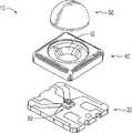
图1A是根据本发明一实施例的半导体晶片封装10的透视图,且图1B是图1A中的半导体封装的分解透视图。参看图1A和1B,本发明的发光晶片封装10包含底部散热体20、顶部散热体40和透镜50。FIG. 1A is a perspective view of a
图2A至2D中更加详细地说明底部散热体20。图2A、2B、2C和2D分别提供图1A中的底部散热体20的顶视图、侧视图、前视图和仰视图。此外,图2C除了展示底部散热体20的前视图之外,还展示了LED组合件60。LED组合件60在图1B中也有说明。参看图1A至2D,底部散热体20为电迹线22和24、焊垫26、32和34以及LED组合件60提供支撑。因此,底部散热体20也称为衬底20。在图中,为了避免混乱,只有代表性焊垫26、32和34标有参考数字。迹线22和24以及焊垫26、32和34可用传导材料制造。此外,可在衬底20的顶部、侧面或底部上制造额外迹线和连接件,或者将其布层在衬底20内部。迹线22和24、焊垫26、32和34以及其他任何连接件可以用已知方法(例如通孔)以任何组合形式彼此互连。The
在有些实施例中,衬底20可由具有高导热性但电绝缘的材料制成,例如氮化铝(AlN)或氧化铝(Al2O3)。在其他实施例中,例如下文结合图7A至10B描述的实施例中,衬底20可包括一种既导电又导热的材料。在此类实施例中,金属引线、传导迹线22和24或者二者可通过形成在衬底部分上的绝缘膜而与衬底绝缘,以下将进行更详细的描述。衬底20的尺寸可根据用来制造晶片封装10的应用和工艺而广泛变化。例如,在所说明的实施例中,衬底20的尺寸可在数毫米(mm)到数十毫米之间变化。虽然本发明并不局限于特定尺寸,但本发明的晶片封装10的一个特定实施例在图中说明为具有其中所示的尺寸。图中所示的所有尺寸均以毫米(用于长度、宽度、高度和半径)和度(用于角度)计算,除非图中、此处的说明书中或二者中另有所指。In some embodiments,
衬底20具有顶面21,顶面21包含电迹线22和24。迹线22和24提供从焊垫(例如顶部焊垫26)到安装垫28的电连接。顶部焊垫26可包括迹线22和24的大体上靠近衬底20侧面的部分。顶部焊垫26电连接到侧焊垫32。安装垫28是顶面(包含迹线22、迹线24或二者的部分)的一部分,LED组合件60安装在其上。安装垫28通常大体上位于邻近顶面21中心处。在本发明的替代实施例中,LED组合件60可由其他半导体电路或晶片代替。
迹线22和24提供电路线以允许LED组合件60电连接到焊垫26、32或34。因此,有些迹线称为第一迹线22,而其他迹线称为第二迹线24。在所说明的实施例中,安装垫28包含第一迹线22和第二迹线24二者的部分。在所说明的实例中,LED组合件60放置在安装垫28的第一迹线22部分上,从而与第一迹线22接触。在所说明的实施例中,LED组合件60的顶部和第二迹线24通过接合线62彼此连接。根据LED组合件60的构造和方位,第一迹线22可提供LED组合件60的阳极(正极)连接,且第二迹线24可包括LED组合件60的阴极(负极)连接,或反之亦然。
LED组合件60可包含额外元件。例如,在图1B和2C中,LED组合件60说明为包含LED接合线62、LED子组合件64和发光二极管(LED)66。此LED子组合件64在所属领域中是已知的,并且是为论述本发明的目的加以说明,而不是旨在限制本发明。图中,LED组合件60展示为晶片附着到衬底20。在替代实施例中,安装垫28可配置成允许LED组合件60的倒装晶片附着。此外,多个LED组合件可安装在安装垫28上。在替代实施例中,LED组合件60可安装在多个迹线上。如果使用倒装晶片技术的话尤其如此。
迹线22和24的布局可能与图中所说明的布局大不相同,但仍然属于本发明的范畴。图中展示了三个单独的阴极(负极)迹线24,以说明三个LED组合件可放置在安装垫28上,其中每一个连接到一不同的阴极(负极)迹线;因此,这三个LED组合件可单独电性控制。迹线22和24由传导材料制成,例如金、银、锡或其他金属。迹线22和24可具有图中所说明的尺寸,且根据应用而定具有数微米或数十微米的厚度。例如,迹线22和24可为15微米厚。图1A和2A说明一方位标记27。此种标记可用来识别晶片封装10的正确方位,即使在晶片封装10组装之后也是如此。如图所示,迹线22和24可从安装垫28延伸到衬底20侧面。The layout of
继续参看图1A至2D,衬底20界定半圆柱空间23和邻近其侧面的四分之一圆柱空间25。图中为避免混乱起见,只有代表性空间23和25标有参考数字。半圆柱空间23和四分之一圆柱空间25为焊料提供空间,以便当晶片封装10附着到印刷电路板(PCB)或另一装置(未图示)(晶片封装10是其组件)时,焊料可在所述空间中流动并在其中凝固。此外,半圆柱空间23和四分之一圆柱空间25在制造过程中提供便利的轮廓和分隔点。With continued reference to FIGS. 1A-2D ,
衬底20可制造成一具有复数个相邻区段的条带中的一个个别区段,其中每个区段均为一衬底20。或者,衬底20可制造成一个由区段阵列组成的个别区段,所述阵列具有多行和多列相邻区段。在这种构造中,半圆柱空间23和四分之一圆柱空间25可在制造过程中用作所述条带或阵列的把手。
此外,半圆柱空间23和四分之一圆柱空间25(与区段之间的划线凹槽或其他蚀刻相结合)辅助将每一单个衬底与条带或晶圆隔开。可通过弯曲条带或晶圆向蚀刻线(越过半圆柱空间23和四分之一圆柱空间25)引入物理应力而实现所述隔离。因制造过程中无需用特殊载体夹具来操作条带或晶圆,所以这些特征简化了制造过程并进而降低了成本。此外,半圆柱空间23和四分之一圆柱空间25可充当通孔,将顶部焊垫26、侧部焊垫32和底部焊垫34连接起来。In addition,
衬底20具有一包含热接触垫36的底面29。所述热接触垫可用导热率较高的材料制造,例如金、银、锡或其他包含但不限于贵金属的材料。
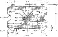
图3说明图1A和1B的半导体封装的部分的剖视侧视图。确切而言,图3说明顶部散热体40和透镜50的剖视侧视图。参看图1A、1B和3,顶部散热体40由导热率较高的材料制成,例如铝、铜、陶瓷、塑料、复合物或这些材料的组合物。可用高温、机械硬度大的介电材料涂覆迹线22和24(中央晶片附着区域除外),以便密封迹线22和24并保护其免受物理和环境损害,例如刮划和氧化。所述涂覆处理可以是衬底制造工艺的组成部分。当使用所述涂覆物时,其也可将衬底20与顶部散热体40绝缘。随后,可用高温胶粘剂(例如,THERMOSET制造的热界面材料)覆盖所述涂覆物,所述胶粘剂将衬底20与顶部散热体40接合。3 illustrates a cross-sectional side view of a portion of the semiconductor package of FIGS. 1A and 1B . Specifically, FIG. 3 illustrates a cut-away side view of
顶部散热体40可包含反射表面42,其大体上围绕安装在安装垫28(图2A和2C中的)上的LED组合件60。反射表面42反射来自LED组合件60的光的部分,如样本光线63所说明。光的其他部分不经反射表面42反射,如样本光线61所说明。说明性光线61和63并不意图代表光学领域中经常使用的光迹线。为了有效地反射光,顶部散热体40优选由可抛光、可印花或既可抛光又可印花的材料制成。或者,为了获得高反射率,光学反射表面42或整个散热体40可用高反射材料电镀或沉积,例如银、铝或另一满足所述目的的物质。因此,顶部散热体40也称为反射板40。如果且当封装10的热性能需要时,反射板40可由导热率较高的材料制成。
在所说明的实施例中,反射表面42说明为平坦表面,其与反射板的水平面成例如45度的角。本发明并不局限于所说明的实施例。例如,反射表面42可与反射板的水平面成其他角度。或者,反射板可具有抛物线或另一形状。In the illustrated embodiment,
反射板40包含边缘44,用以支撑透镜50并与之耦合。LED组合件60用包封材料46(例如,仅举例而言,硅酮)包封在晶片封装10(图1A和1B中)内。包封材料46优选为高温聚合物,其具有高透光率和与透镜50的折射率相匹配的折射率。
透镜50由具有高透光率的材料制成,例如(仅举例而言)玻璃、石英、高温塑料或这些材料的组合物。透镜50可放置成与包封材料46接触。因此,由于晶片封装10受热且经受热膨胀,所以透镜50可由包封材料46缓冲,以保护透镜50免受晶片封装10其他部件热膨胀所导致的机械应力的损害。在有些实施例中,透镜50界定一浅槽52,所述浅槽中可填有光学化学制品,例如磷光体、例如碳酸钙的散光剂、例如荧光材料的中心频率变换材料,或这些材料的组合物。
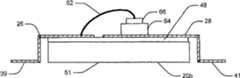
图4说明一耦合到外部散热体70的晶片封装10。参看图4,可使用环氧树脂、焊料或其他导热胶粘剂、导电胶粘剂或导热且导电的胶粘剂74将热接触垫36附着到外部散热体70。外部散热体70可为印刷电路板(PCB)或其他从晶片封装10吸热的结构。所述外部散热体可包含电路元件(未图示)或各种构造的散热翼片72。FIG. 4 illustrates a
图5至6D中展示本发明的一具有特定替代配置的实施例。此第二实施例的部分与图1A至4说明的第一实施例的相应部分相似。为方便起见,图5至6D中说明的第二实施例中与第一实施例相似的部分用相同参考数字表示,类似但有所变化的部分用附有字母“a”的相同参考数字表示,而不同部分则用不同的参考数字表示。An embodiment of the present invention having a certain alternative configuration is shown in Figures 5-6D. Portions of this second embodiment are similar to corresponding portions of the first embodiment illustrated in FIGS. 1A to 4 . For convenience, in the second embodiment illustrated in FIGS. 5 to 6D, like parts of the first embodiment are denoted by the same reference numerals, and similar but changed parts are denoted by the same reference numerals appended with the letter "a", Different parts are indicated by different reference numerals.
图5是根据本发明的其他实施例的LED晶片封装10a的分解透视图。参看图5,本发明的发光晶片封装10a包含底部散热体(衬底)20a、顶部散热体(反射板)40a和透镜50。Fig. 5 is an exploded perspective view of an
图6A、6B、6C和6D分别提供图5中的衬底20a的顶视图、侧视图、前视图和仰视图。参看图5至图6D,在所说明的实施例中,衬底20a包含一个正极迹线22a和四个负极迹线24a。这些迹线22a和24a的构造与图2A中的迹线22和24不同。衬底20a包含凸缘31,其界定闩锁空间33,用以接受反射板40a的支架(leg)35,从而将反射板40a与衬底20a机械啮合。6A, 6B, 6C and 6D provide top, side, front and bottom views, respectively, of
图7A至10B中说明本发明的其他实施例。根据这些实施例,用于高电力发光设备的衬底包含一导热且导电的板,其具有第一和第二表面。所述板可包括金属,例如铜、铝或任一者的合金。所述金属板的第一表面上形成有一较薄的导热绝缘膜。在有些实施例中,所述导热绝缘膜包括陶瓷/聚合物膜,例如可从USA,MN的The Bergquist Company of Chanhassen购买的Thermal Clad膜。Other embodiments of the invention are illustrated in Figures 7A to 10B. According to these embodiments, a substrate for a high power light emitting device includes a thermally and electrically conductive plate having first and second surfaces. The plate may comprise a metal such as copper, aluminum or an alloy of either. A thinner heat conducting and insulating film is formed on the first surface of the metal plate. In some embodiments, the thermally conductive insulating film comprises a ceramic/polymer film, such as Thermal Clad film commercially available from The Bergquist Company of Chanhassen, USA, MN.
可在所述陶瓷/聚合物膜上形成传导元件,例如金属迹线和/或金属引线。由于所述陶瓷/聚合物膜是绝缘的,所以所述传导迹线与金属板没有电接触。一传导元件可形成或电连接到一安装垫,所述安装垫经调整以用于接收电子设备。如以上结合图1至6说明的实施例所述,金属迹线的布局可广泛变化而仍然属于本发明的范畴。Conductive elements, such as metal traces and/or metal leads, may be formed on the ceramic/polymer film. Since the ceramic/polymer film is insulating, the conductive traces have no electrical contact with the metal plate. A conductive element may form or be electrically connected to a mounting pad adapted to receive an electronic device. As described in the embodiments described above in conjunction with FIGS. 1-6 , the layout of the metal traces can vary widely while remaining within the scope of the present invention.
可通过焊接、热超声波接合或热压接合将LED组合件接合到安装垫。LED产生的热量中至少有一部分可以通过所述金属板驱散。由于衬底本身可以充当散热体,所以可以减少或免去将额外散热体接合到所述结构的需要。然而,可将一额外散热体放置成与金属板热连通,以便可更加有效地从运作设备中吸热。The LED assembly can be bonded to the mounting pad by welding, thermosonic bonding, or thermocompression bonding. At least some of the heat generated by the LEDs can be dissipated through the metal plate. Since the substrate itself can act as a heat sink, the need to bond an additional heat sink to the structure can be reduced or eliminated. However, an additional heat sink can be placed in thermal communication with the metal plate so that heat can be drawn more efficiently from the operating equipment.
在一个实施例中,可穿过绝缘膜和金属板形成一个或一个以上通孔。所述通孔内部可涂覆有绝缘材料,例如陶瓷/聚合物膜。可在所述通孔中形成例如导电迹线的电导体,且所述电导体可将衬底的第一表面上的传导元件电连接到衬底的第二表面上的传导元件。根据此种实施例的衬底可在不使用金属引线的情况下安装在一表面(例如印刷电路板)上,这样可获得更加机械坚固的封装。In one embodiment, one or more via holes may be formed through the insulating film and the metal plate. The interior of the via hole may be coated with an insulating material, such as a ceramic/polymer film. An electrical conductor, such as a conductive trace, can be formed in the via and can electrically connect the conductive element on the first surface of the substrate to the conductive element on the second surface of the substrate. A substrate according to such an embodiment can be mounted on a surface, such as a printed circuit board, without the use of metal leads, which results in a more mechanically robust package.
根据本发明实施例的衬底也可包含例如离散齐纳二极管和/或电阻器网络的电子电路,用以静电放电(ESD)和/或过压保护。Substrates according to embodiments of the invention may also contain electronic circuitry such as discrete Zener diodes and/or resistor networks for electrostatic discharge (ESD) and/or overvoltage protection.
虽然图7至10中未予说明,但所述衬底可进一步包含例如半圆柱和四分之一圆柱空间、方位标记、侧接合垫、凸缘或图1至6中说明的其他特征的特征。Although not illustrated in FIGS. 7-10, the substrate may further include features such as half-cylindrical and quarter-cylindrical spaces, orientation marks, side bonding pads, flanges, or other features illustrated in FIGS. 1-6. .
图7A至10B中说明的实施例的部分与图1至6D中说明的实施例的相应部分相似。为方便起见,图7A至10B中说明的实施例中与第一实施例部分相似的部分用相同参考数字表示,类似但有所变化的部分用附有字母“b”的相同参考数字表示,而不同部分则用不同的参考数字表示。Portions of the embodiment illustrated in FIGS. 7A to 10B are similar to corresponding portions of the embodiment illustrated in FIGS. 1 to 6D. For convenience, in the embodiment illustrated in FIGS. 7A to 10B , parts similar to those of the first embodiment are denoted by the same reference numerals, similar but changed parts are denoted by the same reference numerals appended with the letter "b", and Different parts are indicated by different reference numerals.
现在参看图7A,图中说明了根据本发明另一实施例的衬底20b。图7A和7B分别提供衬底20b的顶视图和前视图。另外,除衬底20b的前视图之外,图7B还展示了LED组合件60。衬底20b包含导热且导电的板51,其具有第一和第二表面51a和51b。板51可包括例如铜、铝或任一者的合金的金属。金属板51的第一表面51a的至少若干部分上形成有较薄的导热绝缘膜48。在有些实施例中,导热绝缘膜48包括陶瓷/聚合物膜,例如可从USA,MN的The Bergquist Company of Chanhassen购买的Thermal Clad膜。此外,可在板51的第二表面51b以及侧面上形成导热绝缘膜49。Referring now to FIG. 7A, there is illustrated a
衬底20b为例如电迹线22和24的导电元件、焊垫26和LED组合件60提供支撑。此外,可在衬底20b的顶部、侧面或底部上制造额外迹线和连接件,或者将其布层在衬底20b内部。迹线22和24,焊垫26以及其他任何连接件可以用已知方法(例如通孔)以任何组合形式彼此互连。
衬底20b具有顶面21b,顶面21b包含电迹线22和24。迹线22和24提供从焊垫(例如顶部焊垫26)到安装垫28的电连接。顶部焊垫26可包括迹线22和24大体上邻近衬底20b侧面的部分。安装垫28是顶面(包含迹线22、迹线24或二者的部分)的一部分,LED组合件60安装在其上。安装垫28通常大体上位于邻近顶面21b中心处。在本发明的替代实施例中,LED组合件60可由其他半导体电路或晶片代替。
迹线22和24的布局可能与图中所说明的布局大不相同,但仍然属于本发明的范畴。图中只展示了一个阴极(负极)和一个阳极(正极)迹线。然而,可在衬底20b上包含多个阴极或阳极迹线,以便于在安装垫28上安装复数个LED组合件,每一个均连接到不同阴极或阳极迹线;因此,三个LED组合件可单独地电性控制。迹线22和24由例如金、银、锡或其他金属的传导材料制成。The layout of
衬底20b具有一底面29b,其包含一热接触垫36。所述热接触垫可用导热率较高的材料制造,例如金、银、锡或其他包含但不限于贵金属的材料。
图7C说明沿图7A中的剖面线A-A截取的衬底20b部分的剖视前视图。如图7C中所示,可穿过衬底20b形成一个或一个以上通孔45a、45b。通孔45a、45b的内部可涂覆有例如陶瓷/聚合物膜的绝缘材料。可在通孔中形成例如导电迹线47a、47b的电导体,且所述电导体可将衬底第一表面上的传导元件电连接到衬底第二表面上的传导元件。如图7C中所说明,通孔45a中的传导迹线47a将衬底20b的第一侧面21b或顶面21b上的迹线24连接到衬底20b的第二侧面29b或底面29b上的焊垫34。同样,穿过通孔45b延伸的传导迹线47b将传导迹线22连接到接合垫38。FIG. 7C illustrates a cross-sectional front view of a portion of
根据此实施例的衬底可在不使用金属引线的情况下安装在一表面(例如印刷电路板)上,这样可获得更加机械坚固的封装。A substrate according to this embodiment can be mounted on a surface such as a printed circuit board without the use of metal leads, which results in a more mechanically robust package.
如上所述,可用高温、机械硬度大的介电材料涂覆迹线22和24(中央晶片附着区域28除外),以便密封迹线22和24并保护其免受物理和环境损害,例如刮划和氧化。所述涂覆处理可以是衬底制造工艺的组成部分。当使用所述涂覆物时,其也可将迹线22和24与顶部散热体40绝缘。随后,可用高温胶粘剂(例如,THERMOSET制造的热界面材料)覆盖所述涂覆物,所述胶粘剂将衬底20b与顶部散热体40接合。As noted above, traces 22 and 24 (except central die attach area 28) may be coated with a high temperature, mechanically stiff dielectric material to seal
图8和9中说明未利用通孔的其他实施例。如图8所说明,传导迹线22、24可形成或附着到金属引线39、41,其从封装中延伸出去且可直接安装到电路板。在此实施例中,只有衬底20b的第一表面21b可包含电绝缘、热传导膜48。Other embodiments that do not utilize vias are illustrated in FIGS. 8 and 9 . As illustrated in FIG. 8, conductive traces 22, 24 may be formed or attached to metal leads 39, 41 that extend out of the package and may be mounted directly to the circuit board. In this embodiment, only the
图9说明一实施例,其中传导迹线22、24从衬底20b的侧壁向下延伸,以接触衬底20b第二表面上的接合垫34和38。这种配置可允许在无需使用金属引线或通孔的情况下将封装直接安装到电路板上。9 illustrates an embodiment in which conductive traces 22, 24 extend down from the sidewalls of
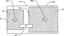
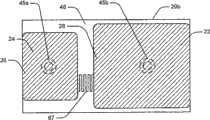
如图10A和10B中所说明,衬底20b可配置成包含例如离散齐纳二极管65、电阻器网络67、其他电子元件或其任何组合物的电子电路。所述电子电路可连接在迹线22和24之间,所述迹线可充当阳极和/或阴极元件。所述电子电路可用于各种目的,例如用以防止静电放电(ESD)、过压保护或二者。在所说明的实例中,图10B中说明的连接在迹线22与迹线24之间的齐纳二极管D1 65可防止过量反向电压施加到衬底20b上安装的光电设备。同样,例如印刷电阻器67的电阻器网络67可向衬底20上安装的设备提供ESD保护。As illustrated in FIGS. 10A and 10B ,
根据以上内容可知,本发明显然是新颖的并且提供超出当前技术的优势。虽然以上描述并说明了本发明的特定实施例,但本发明并不局限于所描述和说明的部件的特定形式和配置。例如,可使用不同的配置、尺寸或材料来实践本发明。本发明受随附权利要求书的限制。在权利要求书中,那些利用用以提供35 USC第112节“的构件或步骤”的权利要求用短语“用以……的构件”来标识。From the foregoing it is evident that the present invention is novel and provides advantages over the prior art. While specific embodiments of the invention have been described and illustrated, the invention is not to be limited to the specific form and arrangement of components described and illustrated. For example, the invention may be practiced using different configurations, dimensions or materials. The invention is limited by the appended claims. In the claims, those claims utilizing "means or steps for providing" 35 USC § 112 are identified by the phrase "means for."
Claims (12)
Applications Claiming Priority (3)
| Application Number | Priority Date | Filing Date | Title |
|---|---|---|---|
| US10/692,351US7244965B2 (en) | 2002-09-04 | 2003-10-22 | Power surface mount light emitting die package |
| US10/692,351 | 2003-10-22 | ||
| CN2004800309433ACN1871710B (en) | 2003-10-22 | 2004-10-20 | Light-emitting chip package with electrical surface mount |
Related Parent Applications (1)
| Application Number | Title | Priority Date | Filing Date |
|---|---|---|---|
| CN2004800309433ADivisionCN1871710B (en) | 2003-10-22 | 2004-10-20 | Light-emitting chip package with electrical surface mount |
Publications (2)
| Publication Number | Publication Date |
|---|---|
| CN102148316Atrue CN102148316A (en) | 2011-08-10 |
| CN102148316B CN102148316B (en) | 2016-01-20 |
Family
ID=34549896
Family Applications (2)
| Application Number | Title | Priority Date | Filing Date |
|---|---|---|---|
| CN2004800309433AExpired - LifetimeCN1871710B (en) | 2003-10-22 | 2004-10-20 | Light-emitting chip package with electrical surface mount |
| CN201110021562.0AExpired - LifetimeCN102148316B (en) | 2003-10-22 | 2004-10-20 | The luminescent wafer encapsulation adopting ammeter face to install |
Family Applications Before (1)
| Application Number | Title | Priority Date | Filing Date |
|---|---|---|---|
| CN2004800309433AExpired - LifetimeCN1871710B (en) | 2003-10-22 | 2004-10-20 | Light-emitting chip package with electrical surface mount |
Country Status (10)
| Country | Link |
|---|---|
| US (5) | US7244965B2 (en) |
| EP (2) | EP2139051B1 (en) |
| JP (1) | JP4602345B2 (en) |
| KR (4) | KR101160037B1 (en) |
| CN (2) | CN1871710B (en) |
| AT (1) | ATE444568T1 (en) |
| CA (1) | CA2549822A1 (en) |
| DE (1) | DE602004023409D1 (en) |
| TW (6) | TWI495143B (en) |
| WO (1) | WO2005043627A1 (en) |
Cited By (8)
| Publication number | Priority date | Publication date | Assignee | Title |
|---|---|---|---|---|
| CN103227274A (en)* | 2012-01-31 | 2013-07-31 | 长春藤控股有限公司 | Packaging body for LED wafer and manufacturing method of packaging body |
| CN103515520A (en)* | 2012-06-29 | 2014-01-15 | 展晶科技(深圳)有限公司 | Light emitting diode encapsulating structure and manufacturing method thereof |
| CN103887420A (en)* | 2014-04-18 | 2014-06-25 | 苏州东山精密制造股份有限公司 | LED packaging structure and LED manufacturing method |
| CN104040741A (en)* | 2011-11-15 | 2014-09-10 | 克利公司 | Light Emitting Diode (LED) Packages And Related Methods |
| CN106463599A (en)* | 2014-04-07 | 2017-02-22 | 皇家飞利浦有限公司 | Lighting device comprising a thermally conductive body and a semiconductor light emitting device |
| CN106571418A (en)* | 2015-10-08 | 2017-04-19 | 世迈克琉明有限公司 | Semiconductor light emitting device |
| CN106848033A (en)* | 2011-05-13 | 2017-06-13 | Lg伊诺特有限公司 | Light emitting device package |
| CN111525017A (en)* | 2020-07-03 | 2020-08-11 | 华引芯(武汉)科技有限公司 | A high light-efficiency flip-chip LED all-inorganic device and its manufacturing method |
Families Citing this family (409)
| Publication number | Priority date | Publication date | Assignee | Title |
|---|---|---|---|---|
| US6633120B2 (en)* | 1998-11-19 | 2003-10-14 | Unisplay S.A. | LED lamps |
| CN100468791C (en) | 2002-08-30 | 2009-03-11 | 吉尔科有限公司 | Light emitting diode with improved effience |
| US10340424B2 (en) | 2002-08-30 | 2019-07-02 | GE Lighting Solutions, LLC | Light emitting diode component |
| US7800121B2 (en) | 2002-08-30 | 2010-09-21 | Lumination Llc | Light emitting diode component |
| US7244965B2 (en)* | 2002-09-04 | 2007-07-17 | Cree Inc, | Power surface mount light emitting die package |
| US7264378B2 (en)* | 2002-09-04 | 2007-09-04 | Cree, Inc. | Power surface mount light emitting die package |
| US7775685B2 (en)* | 2003-05-27 | 2010-08-17 | Cree, Inc. | Power surface mount light emitting die package |
| US7692206B2 (en)* | 2002-12-06 | 2010-04-06 | Cree, Inc. | Composite leadframe LED package and method of making the same |
| US6897486B2 (en) | 2002-12-06 | 2005-05-24 | Ban P. Loh | LED package die having a small footprint |
| USD520965S1 (en)* | 2003-01-10 | 2006-05-16 | Citizen Electronics Co., Ltd. | Light emitting diode for illuminating an object |
| CA2523544A1 (en) | 2003-04-30 | 2004-11-18 | Cree, Inc. | High powered light emitter packages with compact optics |
| AT501081B8 (en)* | 2003-07-11 | 2007-02-15 | Tridonic Optoelectronics Gmbh | LED AS WELL AS LED LIGHT SOURCE |
| US7183587B2 (en)* | 2003-09-09 | 2007-02-27 | Cree, Inc. | Solid metal block mounting substrates for semiconductor light emitting devices |
| FR2862424B1 (en)* | 2003-11-18 | 2006-10-20 | Valeo Electronique Sys Liaison | DEVICE FOR COOLING AN ELECTRICAL COMPONENT AND METHOD FOR MANUFACTURING THE SAME |
| US7518158B2 (en)* | 2003-12-09 | 2009-04-14 | Cree, Inc. | Semiconductor light emitting devices and submounts |
| KR100586944B1 (en)* | 2003-12-26 | 2006-06-07 | 삼성전기주식회사 | High power light emitting diode package and manufacturing method |
| US7517728B2 (en)* | 2004-03-31 | 2009-04-14 | Cree, Inc. | Semiconductor light emitting devices including a luminescent conversion element |
| US7279346B2 (en)* | 2004-03-31 | 2007-10-09 | Cree, Inc. | Method for packaging a light emitting device by one dispense then cure step followed by another |
| KR100655894B1 (en)* | 2004-05-06 | 2006-12-08 | 서울옵토디바이스주식회사 | Wavelength conversion light emitting device with excellent color temperature and color rendering |
| KR100658700B1 (en) | 2004-05-13 | 2006-12-15 | 서울옵토디바이스주식회사 | Light emitting device combining RGB light emitting element and phosphor |
| JP5366399B2 (en)* | 2004-05-31 | 2013-12-11 | オスラム オプト セミコンダクターズ ゲゼルシャフト ミット ベシュレンクテル ハフツング | Optoelectronic semiconductor component and casing substrate for the component |
| DE102004040468B4 (en)* | 2004-05-31 | 2022-02-03 | OSRAM Opto Semiconductors Gesellschaft mit beschränkter Haftung | Optoelectronic semiconductor component and housing base body for such a component |
| US7456499B2 (en)* | 2004-06-04 | 2008-11-25 | Cree, Inc. | Power light emitting die package with reflecting lens and the method of making the same |
| US7280288B2 (en) | 2004-06-04 | 2007-10-09 | Cree, Inc. | Composite optical lens with an integrated reflector |
| US8308980B2 (en)* | 2004-06-10 | 2012-11-13 | Seoul Semiconductor Co., Ltd. | Light emitting device |
| KR100665298B1 (en)* | 2004-06-10 | 2007-01-04 | 서울반도체 주식회사 | Light emitting device |
| KR100665299B1 (en)* | 2004-06-10 | 2007-01-04 | 서울반도체 주식회사 | Emitting material |
| US20050280016A1 (en)* | 2004-06-17 | 2005-12-22 | Mok Thye L | PCB-based surface mount LED device with silicone-based encapsulation structure |
| TWD113473S1 (en)* | 2004-06-24 | 2006-10-21 | 西鐵城電子股份有限公司 | Light emitting diode |
| JP2008504711A (en)* | 2004-06-29 | 2008-02-14 | コーニンクレッカ フィリップス エレクトロニクス エヌ ヴィ | Light emitting diode module |
| USD512694S1 (en)* | 2004-06-30 | 2005-12-13 | Samsung Electro-Mechanics Co., Ltd. | Light-emitting diode |
| US7329905B2 (en)* | 2004-06-30 | 2008-02-12 | Cree, Inc. | Chip-scale methods for packaging light emitting devices and chip-scale packaged light emitting devices |
| US7534633B2 (en) | 2004-07-02 | 2009-05-19 | Cree, Inc. | LED with substrate modifications for enhanced light extraction and method of making same |
| KR100604469B1 (en)* | 2004-08-25 | 2006-07-25 | 박병재 | Light emitting device, package structure and manufacturing method |
| JP2006100787A (en)* | 2004-08-31 | 2006-04-13 | Toyoda Gosei Co Ltd | Light emitting device and light emitting element |
| CN100433383C (en)* | 2004-08-31 | 2008-11-12 | 丰田合成株式会社 | Light emitting device and light emitting element |
| JP4254669B2 (en)* | 2004-09-07 | 2009-04-15 | 豊田合成株式会社 | Light emitting device |
| DE102004047061B4 (en) | 2004-09-28 | 2018-07-26 | Osram Opto Semiconductors Gmbh | Optoelectronic component and method for producing an optoelectronic component |
| US7891836B2 (en)* | 2004-10-22 | 2011-02-22 | Koninklijke Philips Electronics N.V. | Semiconductor light-emitting device with improved heatsinking |
| US20060097385A1 (en)* | 2004-10-25 | 2006-05-11 | Negley Gerald H | Solid metal block semiconductor light emitting device mounting substrates and packages including cavities and heat sinks, and methods of packaging same |
| WO2006046655A1 (en)* | 2004-10-27 | 2006-05-04 | Kyocera Corporation | Light emitting element mounting board, light emitting element storing package, light emitting device and lighting equipment |
| US7772609B2 (en)* | 2004-10-29 | 2010-08-10 | Ledengin, Inc. (Cayman) | LED package with structure and materials for high heat dissipation |
| US7670872B2 (en)* | 2004-10-29 | 2010-03-02 | LED Engin, Inc. (Cayman) | Method of manufacturing ceramic LED packages |
| US7473933B2 (en)* | 2004-10-29 | 2009-01-06 | Ledengin, Inc. (Cayman) | High power LED package with universal bonding pads and interconnect arrangement |
| US8134292B2 (en)* | 2004-10-29 | 2012-03-13 | Ledengin, Inc. | Light emitting device with a thermal insulating and refractive index matching material |
| US9929326B2 (en) | 2004-10-29 | 2018-03-27 | Ledengin, Inc. | LED package having mushroom-shaped lens with volume diffuser |
| US8324641B2 (en)* | 2007-06-29 | 2012-12-04 | Ledengin, Inc. | Matrix material including an embedded dispersion of beads for a light-emitting device |
| US8816369B2 (en) | 2004-10-29 | 2014-08-26 | Led Engin, Inc. | LED packages with mushroom shaped lenses and methods of manufacturing LED light-emitting devices |
| US20060124953A1 (en)* | 2004-12-14 | 2006-06-15 | Negley Gerald H | Semiconductor light emitting device mounting substrates and packages including cavities and cover plates, and methods of packaging same |
| CN100353577C (en)* | 2004-12-14 | 2007-12-05 | 新灯源科技有限公司 | Manufacturing method of light-emitting device with crystal coated light emitting diode |
| US7322732B2 (en)* | 2004-12-23 | 2008-01-29 | Cree, Inc. | Light emitting diode arrays for direct backlighting of liquid crystal displays |
| US9070850B2 (en) | 2007-10-31 | 2015-06-30 | Cree, Inc. | Light emitting diode package and method for fabricating same |
| US9793247B2 (en) | 2005-01-10 | 2017-10-17 | Cree, Inc. | Solid state lighting component |
| US7821023B2 (en) | 2005-01-10 | 2010-10-26 | Cree, Inc. | Solid state lighting component |
| DE602005005223T2 (en)* | 2005-01-12 | 2009-03-12 | Neobulb Technologies Inc. | Lighting device with flip-chip type LEDs and method for its manufacture |
| US7304694B2 (en)* | 2005-01-12 | 2007-12-04 | Cree, Inc. | Solid colloidal dispersions for backlighting of liquid crystal displays |
| US7777247B2 (en)* | 2005-01-14 | 2010-08-17 | Cree, Inc. | Semiconductor light emitting device mounting substrates including a conductive lead extending therein |
| USD515519S1 (en)* | 2005-02-16 | 2006-02-21 | Kabushiki Kaisha Toshiba | Light emitting semiconductor device |
| US7262438B2 (en)* | 2005-03-08 | 2007-08-28 | Avago Technologies Ecbu Ip (Singapore) Pte. Ltd. | LED mounting having increased heat dissipation |
| JP5059739B2 (en)* | 2005-03-11 | 2012-10-31 | ソウル セミコンダクター カンパニー リミテッド | Light emitting diode package having an array of light emitting cells connected in series |
| KR100663906B1 (en)* | 2005-03-14 | 2007-01-02 | 서울반도체 주식회사 | Light emitting device |
| US7879258B2 (en)* | 2005-03-14 | 2011-02-01 | Koninklijke Philips Electronics N.V. | Phosphor in polycrystalline ceramic structure and a light-emitting element comprising same |
| WO2006099741A1 (en)* | 2005-03-24 | 2006-09-28 | Tir Systems Ltd. | Solid-state lighting device package |
| WO2006105638A1 (en)* | 2005-04-05 | 2006-10-12 | Tir Systems Ltd. | Electronic device package with an integrated evaporator |
| JP4595665B2 (en)* | 2005-05-13 | 2010-12-08 | 富士電機システムズ株式会社 | Wiring board manufacturing method |
| CN100391018C (en)* | 2005-06-07 | 2008-05-28 | 吕大明 | LED device and packaging method thereof |
| US8669572B2 (en)* | 2005-06-10 | 2014-03-11 | Cree, Inc. | Power lamp package |
| US7980743B2 (en) | 2005-06-14 | 2011-07-19 | Cree, Inc. | LED backlighting for displays |
| US20060292747A1 (en)* | 2005-06-27 | 2006-12-28 | Loh Ban P | Top-surface-mount power light emitter with integral heat sink |
| TWI287300B (en)* | 2005-06-30 | 2007-09-21 | Lite On Technology Corp | Semiconductor package structure |
| TWI422044B (en)* | 2005-06-30 | 2014-01-01 | Cree Inc | Wafer-scale method for packaging light-emitting device and light-emitting device packaged by wafer scale |
| KR100629521B1 (en)* | 2005-07-29 | 2006-09-28 | 삼성전자주식회사 | LED package and manufacturing method thereof and LED array module using same |
| EP1928030B1 (en)* | 2005-09-20 | 2019-01-30 | Panasonic Intellectual Property Management Co., Ltd. | Led lighting fixture |
| JP2007088155A (en)* | 2005-09-21 | 2007-04-05 | Stanley Electric Co Ltd | Surface mount LED board |
| US20070080360A1 (en)* | 2005-10-06 | 2007-04-12 | Url Mirsky | Microelectronic interconnect substrate and packaging techniques |
| KR101241650B1 (en) | 2005-10-19 | 2013-03-08 | 엘지이노텍 주식회사 | Package of light emitting diode |
| KR101258397B1 (en)* | 2005-11-11 | 2013-04-30 | 서울반도체 주식회사 | Copper-Alkaline-Earth-Silicate mixed crystal phosphors |
| USD531140S1 (en)* | 2005-11-14 | 2006-10-31 | Kabushiki Kaisha Toshiba | Light emitting semiconductor device |
| WO2007059657A1 (en)* | 2005-11-28 | 2007-05-31 | Jen-Shyan Chen | Package structure of light-emitting diode |
| DE102006010729A1 (en) | 2005-12-09 | 2007-06-14 | Osram Opto Semiconductors Gmbh | Optical component, e.g. for miniature opto-electronic semi-conductor chips, comprises a composite unit of lens and mounting part in different materials |
| KR101055772B1 (en)* | 2005-12-15 | 2011-08-11 | 서울반도체 주식회사 | Light emitting device |
| US7772604B2 (en) | 2006-01-05 | 2010-08-10 | Illumitex | Separate optical device for directing light from an LED |
| US7465069B2 (en)* | 2006-01-13 | 2008-12-16 | Chia-Mao Li | High-power LED package structure |
| US8044412B2 (en) | 2006-01-20 | 2011-10-25 | Taiwan Semiconductor Manufacturing Company, Ltd | Package for a light emitting element |
| US7528422B2 (en)* | 2006-01-20 | 2009-05-05 | Hymite A/S | Package for a light emitting element with integrated electrostatic discharge protection |
| JP4895777B2 (en)* | 2006-01-27 | 2012-03-14 | 京セラ株式会社 | WIRING BOARD FOR LIGHT EMITTING ELEMENT AND LIGHT EMITTING DEVICE |
| CN100556242C (en)* | 2006-02-17 | 2009-10-28 | 莱美光电股份有限公司 | Manufacturing method of separated light-emitting diode circuit board |
| KR100780196B1 (en)* | 2006-02-27 | 2007-11-27 | 삼성전기주식회사 | LED package, circuit board for LED package and manufacturing method thereof |
| US7737634B2 (en)* | 2006-03-06 | 2010-06-15 | Avago Technologies General Ip (Singapore) Pte. Ltd. | LED devices having improved containment for liquid encapsulant |
| TWI303872B (en)* | 2006-03-13 | 2008-12-01 | Ind Tech Res Inst | High power light emitting device assembly with esd preotection ability and the method of manufacturing the same |
| KR100738933B1 (en)* | 2006-03-17 | 2007-07-12 | (주)대신엘이디 | LED module for lighting |
| US7808004B2 (en)* | 2006-03-17 | 2010-10-05 | Edison Opto Corporation | Light emitting diode package structure and method of manufacturing the same |
| TWI449137B (en)* | 2006-03-23 | 2014-08-11 | Ceramtec Ag | Carrier for components or circuits |
| US8206779B2 (en)* | 2006-03-24 | 2012-06-26 | Fujifilm Corporation | Method for producing laminate, polarizing plate, and image display device |
| US7675145B2 (en)* | 2006-03-28 | 2010-03-09 | Cree Hong Kong Limited | Apparatus, system and method for use in mounting electronic elements |
| KR100875443B1 (en) | 2006-03-31 | 2008-12-23 | 서울반도체 주식회사 | Light emitting device |
| JP5091421B2 (en)* | 2006-04-07 | 2012-12-05 | 株式会社東芝 | Semiconductor light emitting device |
| US8373195B2 (en) | 2006-04-12 | 2013-02-12 | SemiLEDs Optoelectronics Co., Ltd. | Light-emitting diode lamp with low thermal resistance |
| US7863639B2 (en)* | 2006-04-12 | 2011-01-04 | Semileds Optoelectronics Co. Ltd. | Light-emitting diode lamp with low thermal resistance |
| US11210971B2 (en) | 2009-07-06 | 2021-12-28 | Cree Huizhou Solid State Lighting Company Limited | Light emitting diode display with tilted peak emission pattern |
| US8748915B2 (en)* | 2006-04-24 | 2014-06-10 | Cree Hong Kong Limited | Emitter package with angled or vertical LED |
| US7635915B2 (en) | 2006-04-26 | 2009-12-22 | Cree Hong Kong Limited | Apparatus and method for use in mounting electronic elements |
| US7655957B2 (en) | 2006-04-27 | 2010-02-02 | Cree, Inc. | Submounts for semiconductor light emitting device packages and semiconductor light emitting device packages including the same |
| US7830608B2 (en)* | 2006-05-20 | 2010-11-09 | Oclaro Photonics, Inc. | Multiple emitter coupling devices and methods with beam transform system |
| US20070268572A1 (en)* | 2006-05-20 | 2007-11-22 | Newport Corporation | Multiple emitter coupling devices and methods with beam transform system |
| US7718991B2 (en)* | 2006-05-23 | 2010-05-18 | Cree Led Lighting Solutions, Inc. | Lighting device and method of making |
| WO2007139781A2 (en)* | 2006-05-23 | 2007-12-06 | Cree Led Lighting Solutions, Inc. | Lighting device |
| US7989823B2 (en)* | 2006-06-08 | 2011-08-02 | Hong-Yuan Technology Co., Ltd. | Light emitting system, light emitting apparatus and forming method thereof |
| US7680170B2 (en)* | 2006-06-15 | 2010-03-16 | Oclaro Photonics, Inc. | Coupling devices and methods for stacked laser emitter arrays |
| US20070291373A1 (en)* | 2006-06-15 | 2007-12-20 | Newport Corporation | Coupling devices and methods for laser emitters |
| USD571315S1 (en)* | 2006-06-19 | 2008-06-17 | Avago Technologies Ecbu Ip (Singapore) Pte Ltd | Light emitting diode |
| USD576966S1 (en) | 2006-06-26 | 2008-09-16 | Avago Technologies General Ip (Singapore) Pte Ltd. | Light emitting diode |
| US8610134B2 (en)* | 2006-06-29 | 2013-12-17 | Cree, Inc. | LED package with flexible polyimide circuit and method of manufacturing LED package |
| US7906794B2 (en)* | 2006-07-05 | 2011-03-15 | Koninklijke Philips Electronics N.V. | Light emitting device package with frame and optically transmissive element |
| US8044418B2 (en)* | 2006-07-13 | 2011-10-25 | Cree, Inc. | Leadframe-based packages for solid state light emitting devices |
| US7960819B2 (en)* | 2006-07-13 | 2011-06-14 | Cree, Inc. | Leadframe-based packages for solid state emitting devices |
| TWM303325U (en)* | 2006-07-13 | 2006-12-21 | Everlight Electronics Co Ltd | Light emitting diode package |
| US8735920B2 (en)* | 2006-07-31 | 2014-05-27 | Cree, Inc. | Light emitting diode package with optical element |
| US7804147B2 (en) | 2006-07-31 | 2010-09-28 | Cree, Inc. | Light emitting diode package element with internal meniscus for bubble free lens placement |
| USD591697S1 (en) | 2006-08-09 | 2009-05-05 | Cree, Inc. | Lamp package |
| US8367945B2 (en)* | 2006-08-16 | 2013-02-05 | Cree Huizhou Opto Limited | Apparatus, system and method for use in mounting electronic elements |
| US7909482B2 (en) | 2006-08-21 | 2011-03-22 | Innotec Corporation | Electrical device having boardless electrical component mounting arrangement |
| KR101258227B1 (en) | 2006-08-29 | 2013-04-25 | 서울반도체 주식회사 | Light emitting device |
| KR100828900B1 (en) | 2006-09-04 | 2008-05-09 | 엘지이노텍 주식회사 | Light emitting diode package and manufacturing method thereof |
| US7842960B2 (en) | 2006-09-06 | 2010-11-30 | Lumination Llc | Light emitting packages and methods of making same |
| US20080074884A1 (en)* | 2006-09-25 | 2008-03-27 | Thye Linn Mok | Compact high-intensty LED-based light source and method for making the same |
| KR100774218B1 (en)* | 2006-09-28 | 2007-11-08 | 엘지전자 주식회사 | Lens, manufacturing method and light emitting device package |
| WO2008042351A2 (en) | 2006-10-02 | 2008-04-10 | Illumitex, Inc. | Led system and method |
| US20090275157A1 (en)* | 2006-10-02 | 2009-11-05 | Illumitex, Inc. | Optical device shaping |
| US7866897B2 (en)* | 2006-10-06 | 2011-01-11 | Oclaro Photonics, Inc. | Apparatus and method of coupling a fiber optic device to a laser |
| BRPI0718086A2 (en)* | 2006-10-31 | 2013-11-05 | Tir Technology Lp | LIGHTING DEVICE PACKAGING |
| US7808013B2 (en)* | 2006-10-31 | 2010-10-05 | Cree, Inc. | Integrated heat spreaders for light emitting devices (LEDs) and related assemblies |
| CN101578711A (en)* | 2006-11-09 | 2009-11-11 | 跃进封装公司 | Leg reflective package |
| US10295147B2 (en) | 2006-11-09 | 2019-05-21 | Cree, Inc. | LED array and method for fabricating same |
| USD576115S1 (en)* | 2006-11-14 | 2008-09-02 | Lg Innotek Co., Ltd. | Light-emitting diode |
| USD594827S1 (en)* | 2006-12-07 | 2009-06-23 | Cree, Inc. | Lamp package |
| DE102006062066A1 (en)* | 2006-12-29 | 2008-07-03 | Osram Opto Semiconductors Gmbh | Lens arrangement for light emitting diode display device, has lens with lens surface and optical axis, which penetrates lens surface of lens |
| US20080158886A1 (en)* | 2006-12-29 | 2008-07-03 | Siew It Pang | Compact High-Intensity LED Based Light Source |
| US8021904B2 (en)* | 2007-02-01 | 2011-09-20 | Cree, Inc. | Ohmic contacts to nitrogen polarity GaN |
| US9711703B2 (en)* | 2007-02-12 | 2017-07-18 | Cree Huizhou Opto Limited | Apparatus, system and method for use in mounting electronic elements |
| US7922360B2 (en)* | 2007-02-14 | 2011-04-12 | Cree, Inc. | Thermal transfer in solid state light emitting apparatus and methods of manufacturing |
| US8408773B2 (en) | 2007-03-19 | 2013-04-02 | Innotec Corporation | Light for vehicles |
| US7712933B2 (en) | 2007-03-19 | 2010-05-11 | Interlum, Llc | Light for vehicles |
| KR100850666B1 (en)* | 2007-03-30 | 2008-08-07 | 서울반도체 주식회사 | LED package with metal PC |
| US7964888B2 (en)* | 2007-04-18 | 2011-06-21 | Cree, Inc. | Semiconductor light emitting device packages and methods |
| WO2008148029A1 (en)* | 2007-05-25 | 2008-12-04 | Molex Incorporated | Heat sink for a heat generator and a power source |
| US20090008662A1 (en)* | 2007-07-05 | 2009-01-08 | Ian Ashdown | Lighting device package |
| US20090008670A1 (en)* | 2007-07-06 | 2009-01-08 | Topco Technologies Corp. | LED packaging structure with aluminum board and an LED lamp with said LED packaging structure |
| US20090008671A1 (en)* | 2007-07-06 | 2009-01-08 | Lustrous Technology Ltd. | LED packaging structure with aluminum board and an LED lamp with said LED packaging structure |
| TWI368336B (en)* | 2007-07-12 | 2012-07-11 | Chi Mei Lighting Tech Corp | Light emitting diode device and applications thereof |
| CN201228949Y (en)* | 2007-07-18 | 2009-04-29 | 胡凯 | LED lamp heat radiation body |
| RU2467051C2 (en) | 2007-08-22 | 2012-11-20 | Сеул Семикондактор Ко., Лтд. | Luminophores based on nonstoichiometric tetragonal silicates of copper and alkali-earth metal and method for production thereof |
| KR101055769B1 (en)* | 2007-08-28 | 2011-08-11 | 서울반도체 주식회사 | Light-emitting device adopting non-stoichiometric tetra-alkaline earth silicate phosphor |
| KR101365621B1 (en) | 2007-09-04 | 2014-02-24 | 서울반도체 주식회사 | Light emitting diode package having heat dissipating slugs |
| CN101388161A (en)* | 2007-09-14 | 2009-03-18 | 科锐香港有限公司 | LED surface mounting device and LED display incorporating the same |
| EP2201615B8 (en) | 2007-09-20 | 2015-01-28 | Philips Intellectual Property & Standards GmbH | Led package and method for manufacturing the led package |
| US9172012B2 (en)* | 2007-10-31 | 2015-10-27 | Cree, Inc. | Multi-chip light emitter packages and related methods |
| US9666762B2 (en) | 2007-10-31 | 2017-05-30 | Cree, Inc. | Multi-chip light emitter packages and related methods |
| US10256385B2 (en)* | 2007-10-31 | 2019-04-09 | Cree, Inc. | Light emitting die (LED) packages and related methods |
| US8866169B2 (en)* | 2007-10-31 | 2014-10-21 | Cree, Inc. | LED package with increased feature sizes |
| US9082921B2 (en) | 2007-10-31 | 2015-07-14 | Cree, Inc. | Multi-die LED package |
| USD615504S1 (en) | 2007-10-31 | 2010-05-11 | Cree, Inc. | Emitter package |
| US8368100B2 (en)* | 2007-11-14 | 2013-02-05 | Cree, Inc. | Semiconductor light emitting diodes having reflective structures and methods of fabricating same |
| US9634191B2 (en) | 2007-11-14 | 2017-04-25 | Cree, Inc. | Wire bond free wafer level LED |
| TWD128525S1 (en)* | 2007-12-05 | 2009-05-01 | 西鐵城電子股份有限公司 | Light-emitting diode for illuminating an object |
| TWD128709S1 (en)* | 2007-12-05 | 2009-05-11 | 西鐵城電子股份有限公司 | Light-emitting diode for illuminating an object |
| WO2009076579A2 (en) | 2007-12-12 | 2009-06-18 | Innotec Corporation | Overmolded circuit board and method |
| US9431589B2 (en) | 2007-12-14 | 2016-08-30 | Cree, Inc. | Textured encapsulant surface in LED packages |
| USD633631S1 (en) | 2007-12-14 | 2011-03-01 | Cree Hong Kong Limited | Light source of light emitting diode |
| US8553737B2 (en)* | 2007-12-17 | 2013-10-08 | Oclaro Photonics, Inc. | Laser emitter modules and methods of assembly |
| EP2073280A1 (en)* | 2007-12-20 | 2009-06-24 | Fraunhofer-Gesellschaft zur Förderung der angewandten Forschung e.V. | Reflective secondary optics and semiconductor components |
| US20090159125A1 (en)* | 2007-12-21 | 2009-06-25 | Eric Prather | Solar cell package for solar concentrator |
| KR20090072941A (en)* | 2007-12-28 | 2009-07-02 | 삼성전기주식회사 | High output LED package and manufacturing method |
| USD634863S1 (en) | 2008-01-10 | 2011-03-22 | Cree Hong Kong Limited | Light source of light emitting diode |
| US10008637B2 (en) | 2011-12-06 | 2018-06-26 | Cree, Inc. | Light emitter devices and methods with reduced dimensions and improved light output |
| US8304660B2 (en)* | 2008-02-07 | 2012-11-06 | National Taiwan University | Fully reflective and highly thermoconductive electronic module and method of manufacturing the same |
| JP2011512037A (en) | 2008-02-08 | 2011-04-14 | イルミテックス, インコーポレイテッド | System and method for emitter layer shaping |
| KR100998009B1 (en) | 2008-03-12 | 2010-12-03 | 삼성엘이디 주식회사 | Light emitting diode package and manufacturing method thereof |
| US8804246B2 (en)* | 2008-05-08 | 2014-08-12 | Ii-Vi Laser Enterprise Gmbh | High brightness diode output methods and devices |
| US8049230B2 (en) | 2008-05-16 | 2011-11-01 | Cree Huizhou Opto Limited | Apparatus and system for miniature surface mount devices |
| JP5320560B2 (en)* | 2008-05-20 | 2013-10-23 | 東芝ライテック株式会社 | Light source unit and lighting device |
| JP5359045B2 (en)* | 2008-06-18 | 2013-12-04 | 日亜化学工業株式会社 | Semiconductor device and manufacturing method thereof |
| TWI384649B (en)* | 2008-06-18 | 2013-02-01 | Harvatek Corp | Light emitting diode chip encapsulation structure with embedded electrostatic protection function and its making method |
| US7851818B2 (en)* | 2008-06-27 | 2010-12-14 | Taiwan Semiconductor Manufacturing Company, Ltd. | Fabrication of compact opto-electronic component packages |
| US20110095328A1 (en)* | 2008-07-01 | 2011-04-28 | Koninklijke Philips Electronics N.V. | Close proximity collimator for led |
| GB2462815A (en)* | 2008-08-18 | 2010-02-24 | Sensitive Electronic Co Ltd | Light emitting diode lamp |
| JP2010067902A (en)* | 2008-09-12 | 2010-03-25 | Toshiba Corp | Light-emitting device |
| US20100078661A1 (en)* | 2008-09-26 | 2010-04-01 | Wei Shi | Machined surface led assembly |
| US7887384B2 (en)* | 2008-09-26 | 2011-02-15 | Bridgelux, Inc. | Transparent ring LED assembly |
| US9252336B2 (en)* | 2008-09-26 | 2016-02-02 | Bridgelux, Inc. | Multi-cup LED assembly |
| US8049236B2 (en)* | 2008-09-26 | 2011-11-01 | Bridgelux, Inc. | Non-global solder mask LED assembly |
| US8058664B2 (en) | 2008-09-26 | 2011-11-15 | Bridgelux, Inc. | Transparent solder mask LED assembly |
| TWI528508B (en)* | 2008-10-13 | 2016-04-01 | 榮創能源科技股份有限公司 | High-power light-emitting diode ceramic package manufacturing method |
| US8075165B2 (en)* | 2008-10-14 | 2011-12-13 | Ledengin, Inc. | Total internal reflection lens and mechanical retention and locating device |
| US9425172B2 (en) | 2008-10-24 | 2016-08-23 | Cree, Inc. | Light emitter array |
| US8791471B2 (en)* | 2008-11-07 | 2014-07-29 | Cree Hong Kong Limited | Multi-chip light emitting diode modules |
| US20100117106A1 (en)* | 2008-11-07 | 2010-05-13 | Ledengin, Inc. | Led with light-conversion layer |
| RU2508498C2 (en)* | 2008-11-18 | 2014-02-27 | Конинклейке Филипс Электроникс Н.В. | Electric lamp |
| KR101041018B1 (en)* | 2008-11-21 | 2011-06-16 | 고견채 | LED lamp with reflector and lamp |
| CN101740675B (en)* | 2008-11-25 | 2012-02-29 | 亿光电子工业股份有限公司 | LED circuit board |
| JP2010153803A (en)* | 2008-11-28 | 2010-07-08 | Toshiba Lighting & Technology Corp | Electronic component mounting module and electrical apparatus |
| US20100142198A1 (en)* | 2008-12-09 | 2010-06-10 | Chih-Wen Yang | Configurable Light Emitting System |
| TW201034256A (en) | 2008-12-11 | 2010-09-16 | Illumitex Inc | Systems and methods for packaging light-emitting diode devices |
| US20100149771A1 (en) | 2008-12-16 | 2010-06-17 | Cree, Inc. | Methods and Apparatus for Flexible Mounting of Light Emitting Devices |
| CN101761795B (en)* | 2008-12-23 | 2011-12-28 | 富准精密工业(深圳)有限公司 | Light-emitting diode illumination device and encapsulation method thereof |
| US8507300B2 (en)* | 2008-12-24 | 2013-08-13 | Ledengin, Inc. | Light-emitting diode with light-conversion layer |
| USD648686S1 (en) | 2010-04-30 | 2011-11-15 | Cree, Inc. | Light emitting diode (LED) package |
| US7923739B2 (en)* | 2009-06-05 | 2011-04-12 | Cree, Inc. | Solid state lighting device |
| USD641719S1 (en) | 2009-06-05 | 2011-07-19 | Cree, Inc. | Light emitting diode |
| US8598602B2 (en)* | 2009-01-12 | 2013-12-03 | Cree, Inc. | Light emitting device packages with improved heat transfer |
| USD621799S1 (en) | 2009-01-12 | 2010-08-17 | Cree, Inc. | Light emitting diode |
| US8368112B2 (en) | 2009-01-14 | 2013-02-05 | Cree Huizhou Opto Limited | Aligned multiple emitter package |
| US10431567B2 (en)* | 2010-11-03 | 2019-10-01 | Cree, Inc. | White ceramic LED package |
| US20110037083A1 (en)* | 2009-01-14 | 2011-02-17 | Alex Chi Keung Chan | Led package with contrasting face |
| JP5340763B2 (en) | 2009-02-25 | 2013-11-13 | ローム株式会社 | LED lamp |
| US8269248B2 (en)* | 2009-03-02 | 2012-09-18 | Thompson Joseph B | Light emitting assemblies and portions thereof |
| WO2010110572A2 (en)* | 2009-03-24 | 2010-09-30 | Kim Kang | Light-emitting diode package |
| US7985000B2 (en)* | 2009-04-08 | 2011-07-26 | Ledengin, Inc. | Lighting apparatus having multiple light-emitting diodes with individual light-conversion layers |
| US8598793B2 (en) | 2011-05-12 | 2013-12-03 | Ledengin, Inc. | Tuning of emitter with multiple LEDs to a single color bin |
| CN101894901B (en) | 2009-04-08 | 2013-11-20 | 硅谷光擎 | Package for multiple light emitting diodes |
| US8957435B2 (en)* | 2009-04-28 | 2015-02-17 | Cree, Inc. | Lighting device |
| US8106569B2 (en)* | 2009-05-12 | 2012-01-31 | Remphos Technologies Llc | LED retrofit for miniature bulbs |
| DE102009023854B4 (en) | 2009-06-04 | 2023-11-09 | OSRAM Opto Semiconductors Gesellschaft mit beschränkter Haftung | Optoelectronic semiconductor component |
| USD648687S1 (en) | 2009-06-05 | 2011-11-15 | Cree, Inc. | Light emitting device package |
| US8686445B1 (en) | 2009-06-05 | 2014-04-01 | Cree, Inc. | Solid state lighting devices and methods |
| US9111778B2 (en) | 2009-06-05 | 2015-08-18 | Cree, Inc. | Light emitting diode (LED) devices, systems, and methods |
| US8860043B2 (en)* | 2009-06-05 | 2014-10-14 | Cree, Inc. | Light emitting device packages, systems and methods |
| TWM370182U (en)* | 2009-06-09 | 2009-12-01 | Advanced Connectek Inc | LED chip holder structure |
| DE102009030205A1 (en)* | 2009-06-24 | 2010-12-30 | Litec-Lp Gmbh | Phosphors with Eu (II) -doped silicate luminophores |
| KR101055762B1 (en)* | 2009-09-01 | 2011-08-11 | 서울반도체 주식회사 | Light-emitting device employing a light-emitting material having an oxyosilicate light emitter |
| JP2011009519A (en)* | 2009-06-26 | 2011-01-13 | Hitachi Chem Co Ltd | Optical semiconductor device and method for manufacturing the optical semiconductor device |
| US8415692B2 (en) | 2009-07-06 | 2013-04-09 | Cree, Inc. | LED packages with scattering particle regions |
| TWD139848S1 (en)* | 2009-07-14 | 2011-04-01 | 東芝照明技術股份有限公司 | Light emitting diode module |
| US8598809B2 (en) | 2009-08-19 | 2013-12-03 | Cree, Inc. | White light color changing solid state lighting and methods |
| US8449128B2 (en) | 2009-08-20 | 2013-05-28 | Illumitex, Inc. | System and method for a lens and phosphor layer |
| US8585253B2 (en) | 2009-08-20 | 2013-11-19 | Illumitex, Inc. | System and method for color mixing lens array |
| US8410371B2 (en)* | 2009-09-08 | 2013-04-02 | Cree, Inc. | Electronic device submounts with thermally conductive vias and light emitting devices including the same |
| CN102576789B (en)* | 2009-09-20 | 2016-08-24 | 维亚甘有限公司 | The wafer-class encapsulation of electronic device |
| US8593040B2 (en) | 2009-10-02 | 2013-11-26 | Ge Lighting Solutions Llc | LED lamp with surface area enhancing fins |
| KR101075774B1 (en)* | 2009-10-29 | 2011-10-26 | 삼성전기주식회사 | Luminous element package and method for manufacturing the same |
| US7893445B2 (en)* | 2009-11-09 | 2011-02-22 | Cree, Inc. | Solid state emitter package including red and blue emitters |
| JP5623062B2 (en) | 2009-11-13 | 2014-11-12 | シャープ株式会社 | Light emitting device and manufacturing method thereof |
| US20110116262A1 (en)* | 2009-11-13 | 2011-05-19 | Phoseon Technology, Inc. | Economical partially collimating reflective micro optical array |
| WO2011060319A1 (en) | 2009-11-13 | 2011-05-19 | Uni-Light Llc | Led thermal management |
| TWI381563B (en)* | 2009-11-20 | 2013-01-01 | Everlight Electronics Co Ltd | Light emitting diode package and manufacturing method thereof |
| KR101163850B1 (en)* | 2009-11-23 | 2012-07-09 | 엘지이노텍 주식회사 | Light emitting device package |
| US10290788B2 (en)* | 2009-11-24 | 2019-05-14 | Luminus Devices, Inc. | Systems and methods for managing heat from an LED |
| US8303141B2 (en)* | 2009-12-17 | 2012-11-06 | Ledengin, Inc. | Total internal reflection lens with integrated lamp cover |
| WO2011091170A2 (en) | 2010-01-22 | 2011-07-28 | Oclaro Photonics, Inc. | Homogenization of far field fiber coupled radiation |
| JP2011151268A (en) | 2010-01-22 | 2011-08-04 | Sharp Corp | Light emitting device |
| US8350370B2 (en) | 2010-01-29 | 2013-01-08 | Cree Huizhou Opto Limited | Wide angle oval light emitting diode package |
| USD640643S1 (en)* | 2010-04-07 | 2011-06-28 | Everlight Electronics Co., Ltd. | Light emitting diode |
| US8362515B2 (en)* | 2010-04-07 | 2013-01-29 | Chia-Ming Cheng | Chip package and method for forming the same |
| USD643381S1 (en)* | 2010-04-07 | 2011-08-16 | Everlight Electronics Co., Ltd. | Light emitting diode |
| US9080729B2 (en) | 2010-04-08 | 2015-07-14 | Ledengin, Inc. | Multiple-LED emitter for A-19 lamps |
| US8858022B2 (en) | 2011-05-05 | 2014-10-14 | Ledengin, Inc. | Spot TIR lens system for small high-power emitter |
| US9345095B2 (en) | 2010-04-08 | 2016-05-17 | Ledengin, Inc. | Tunable multi-LED emitter module |
| CN105720180B (en)* | 2010-04-09 | 2018-05-29 | 罗姆股份有限公司 | Led module |
| USD651989S1 (en)* | 2010-04-09 | 2012-01-10 | Everlight Electronics Co., Ltd. | Light emitting diode |
| US9012938B2 (en) | 2010-04-09 | 2015-04-21 | Cree, Inc. | High reflective substrate of light emitting devices with improved light output |
| US8901583B2 (en) | 2010-04-12 | 2014-12-02 | Cree Huizhou Opto Limited | Surface mount device thin package |
| US9240526B2 (en) | 2010-04-23 | 2016-01-19 | Cree, Inc. | Solid state light emitting diode packages with leadframes and ceramic material |
| US8329482B2 (en) | 2010-04-30 | 2012-12-11 | Cree, Inc. | White-emitting LED chips and method for making same |
| SG10201504616TA (en)* | 2010-06-11 | 2015-07-30 | Ricoh Co Ltd | Information storage device, removable device, developer container, and image forming apparatus |
| DE102010024862A1 (en)* | 2010-06-24 | 2011-12-29 | Osram Opto Semiconductors Gmbh | Optoelectronic semiconductor component |
| US8648359B2 (en) | 2010-06-28 | 2014-02-11 | Cree, Inc. | Light emitting devices and methods |
| US8269244B2 (en) | 2010-06-28 | 2012-09-18 | Cree, Inc. | LED package with efficient, isolated thermal path |
| USD643819S1 (en) | 2010-07-16 | 2011-08-23 | Cree, Inc. | Package for light emitting diode (LED) lighting |
| TWD141204S1 (en) | 2010-07-23 | 2011-06-21 | 億光電子工業股份有限公司 | Light emitting diode |
| US9831393B2 (en)* | 2010-07-30 | 2017-11-28 | Cree Hong Kong Limited | Water resistant surface mount device package |
| US9070851B2 (en) | 2010-09-24 | 2015-06-30 | Seoul Semiconductor Co., Ltd. | Wafer-level light emitting diode package and method of fabricating the same |
| US20120074432A1 (en)* | 2010-09-29 | 2012-03-29 | Amtran Technology Co., Ltd | Led package module and manufacturing method thereof |
| US8455882B2 (en) | 2010-10-15 | 2013-06-04 | Cree, Inc. | High efficiency LEDs |
| CN102456803A (en)* | 2010-10-20 | 2012-05-16 | 展晶科技(深圳)有限公司 | Light-emitting diode packaging structure |
| US8564000B2 (en) | 2010-11-22 | 2013-10-22 | Cree, Inc. | Light emitting devices for light emitting diodes (LEDs) |
| US9300062B2 (en) | 2010-11-22 | 2016-03-29 | Cree, Inc. | Attachment devices and methods for light emitting devices |
| US9490235B2 (en) | 2010-11-22 | 2016-11-08 | Cree, Inc. | Light emitting devices, systems, and methods |
| US9000470B2 (en) | 2010-11-22 | 2015-04-07 | Cree, Inc. | Light emitter devices |
| US8624271B2 (en) | 2010-11-22 | 2014-01-07 | Cree, Inc. | Light emitting devices |
| TWI405936B (en)* | 2010-11-23 | 2013-08-21 | Ind Tech Res Inst | Clamping the opposite seat and its light-emitting diode light board |
| US9240395B2 (en) | 2010-11-30 | 2016-01-19 | Cree Huizhou Opto Limited | Waterproof surface mount device package and method |
| US9822951B2 (en) | 2010-12-06 | 2017-11-21 | Cree, Inc. | LED retrofit lens for fluorescent tube |
| US10309627B2 (en) | 2012-11-08 | 2019-06-04 | Cree, Inc. | Light fixture retrofit kit with integrated light bar |
| US8610140B2 (en) | 2010-12-15 | 2013-12-17 | Cree, Inc. | Light emitting diode (LED) packages, systems, devices and related methods |
| USD679842S1 (en) | 2011-01-03 | 2013-04-09 | Cree, Inc. | High brightness LED package |
| CN102142508A (en)* | 2010-12-16 | 2011-08-03 | 西安炬光科技有限公司 | Encapsulation structure and encapsulation method for high-power and high-brightness LED light source |
| US8772817B2 (en) | 2010-12-22 | 2014-07-08 | Cree, Inc. | Electronic device submounts including substrates with thermally conductive vias |
| US8644357B2 (en) | 2011-01-11 | 2014-02-04 | Ii-Vi Incorporated | High reliability laser emitter modules |
| TW201251140A (en) | 2011-01-31 | 2012-12-16 | Cree Inc | High brightness light emitting diode (LED) packages, systems and methods with improved resin filling and high adhesion |
| CN103348496A (en) | 2011-02-07 | 2013-10-09 | 克利公司 | Components and methods for light emitting diode (LED) lighting |
| USD702653S1 (en) | 2011-10-26 | 2014-04-15 | Cree, Inc. | Light emitting device component |
| TWI424544B (en)* | 2011-03-31 | 2014-01-21 | Novatek Microelectronics Corp | Integrated circuit device |
| EP2695189A1 (en)* | 2011-04-04 | 2014-02-12 | CeramTec GmbH | Ceramic printed circuit board comprising an al cooling body |
| US9518723B2 (en) | 2011-04-08 | 2016-12-13 | Brite Shot, Inc. | Lighting fixture extension |
| CN102769089B (en)* | 2011-05-06 | 2015-01-07 | 展晶科技(深圳)有限公司 | Semiconductor packaging structure |
| DE102011101052A1 (en)* | 2011-05-09 | 2012-11-15 | Heraeus Materials Technology Gmbh & Co. Kg | Substrate with electrically neutral region |
| US8513900B2 (en) | 2011-05-12 | 2013-08-20 | Ledengin, Inc. | Apparatus for tuning of emitter with multiple LEDs to a single color bin |
| KR101869552B1 (en)* | 2011-05-13 | 2018-06-21 | 엘지이노텍 주식회사 | Light emitting device and ultraviolet lamp having the same |
| US10842016B2 (en)* | 2011-07-06 | 2020-11-17 | Cree, Inc. | Compact optically efficient solid state light source with integrated thermal management |
| KR101082587B1 (en)* | 2011-07-07 | 2011-11-17 | 주식회사지엘에스 | LED lighting device |
| US10211380B2 (en) | 2011-07-21 | 2019-02-19 | Cree, Inc. | Light emitting devices and components having improved chemical resistance and related methods |
| US10686107B2 (en) | 2011-07-21 | 2020-06-16 | Cree, Inc. | Light emitter devices and components with improved chemical resistance and related methods |
| JP2014525146A (en) | 2011-07-21 | 2014-09-25 | クリー インコーポレイテッド | Light emitting device, package, component, and method for improved chemical resistance and related methods |
| US8992045B2 (en)* | 2011-07-22 | 2015-03-31 | Guardian Industries Corp. | LED lighting systems and/or methods of making the same |
| TWI437670B (en)* | 2011-08-19 | 2014-05-11 | Subtron Technology Co Ltd | Heat sink substrate structure and process |
| JPWO2013027413A1 (en)* | 2011-08-25 | 2015-03-05 | パナソニック株式会社 | Protective element and light emitting device using the same |
| KR101817807B1 (en)* | 2011-09-20 | 2018-01-11 | 엘지이노텍 주식회사 | Light emitting device package and lighting system including the same |
| KR20140097284A (en) | 2011-11-07 | 2014-08-06 | 크리,인코포레이티드 | High voltage array light emitting diode(led) devices, fixtures and methods |
| US9046241B2 (en) | 2011-11-12 | 2015-06-02 | Jingqun Xi | High efficiency directional light source using lens optics |
| KR101197092B1 (en)* | 2011-11-24 | 2012-11-07 | 삼성전자주식회사 | Light emitting diode package and method for producting the light emitting diode package |
| US8564004B2 (en) | 2011-11-29 | 2013-10-22 | Cree, Inc. | Complex primary optics with intermediate elements |
| US9496466B2 (en) | 2011-12-06 | 2016-11-15 | Cree, Inc. | Light emitter devices and methods, utilizing light emitting diodes (LEDs), for improved light extraction |
| JP6107060B2 (en) | 2011-12-26 | 2017-04-05 | 日亜化学工業株式会社 | Method for manufacturing light emitting device |
| US9343441B2 (en) | 2012-02-13 | 2016-05-17 | Cree, Inc. | Light emitter devices having improved light output and related methods |
| US9240530B2 (en) | 2012-02-13 | 2016-01-19 | Cree, Inc. | Light emitter devices having improved chemical and physical resistance and related methods |
| US11032884B2 (en) | 2012-03-02 | 2021-06-08 | Ledengin, Inc. | Method for making tunable multi-led emitter module |
| US20150040388A1 (en)* | 2012-03-20 | 2015-02-12 | Applied Nanotech Holdings, Inc. | Application of Dielectric Layer and Circuit Traces on Heat Sink |
| US9897284B2 (en) | 2012-03-28 | 2018-02-20 | Ledengin, Inc. | LED-based MR16 replacement lamp |
| FR2988910B1 (en) | 2012-03-28 | 2014-12-26 | Commissariat Energie Atomique | LOW-RTH LED COMPONENT WITH DISSOCATED ELECTRIC AND THERMAL WAYS |
| US10222032B2 (en) | 2012-03-30 | 2019-03-05 | Cree, Inc. | Light emitter components and methods having improved electrical contacts |
| US10134961B2 (en) | 2012-03-30 | 2018-11-20 | Cree, Inc. | Submount based surface mount device (SMD) light emitter components and methods |
| US9735198B2 (en) | 2012-03-30 | 2017-08-15 | Cree, Inc. | Substrate based light emitter devices, components, and related methods |
| CN103367615B (en)* | 2012-04-06 | 2018-02-02 | 日亚化学工业株式会社 | Light-emitting device is with being packaged into body and used its light-emitting device |
| US9188290B2 (en) | 2012-04-10 | 2015-11-17 | Cree, Inc. | Indirect linear fixture |
| US9500355B2 (en) | 2012-05-04 | 2016-11-22 | GE Lighting Solutions, LLC | Lamp with light emitting elements surrounding active cooling device |
| USD711840S1 (en) | 2012-06-11 | 2014-08-26 | Cree, Inc. | LED package |
| DE112013002944T5 (en) | 2012-06-13 | 2015-02-19 | Innotec, Corp. | Flexible hollow fiber optic cable |
| USD725613S1 (en) | 2012-06-15 | 2015-03-31 | Cree, Inc. | LED package |
| USD718258S1 (en) | 2012-09-02 | 2014-11-25 | Cree, Inc. | LED package |
| FI125565B (en)* | 2012-09-08 | 2015-11-30 | Lumichip Ltd | LED chip-on-board component and lighting module |
| KR101974348B1 (en) | 2012-09-12 | 2019-05-02 | 삼성전자주식회사 | Light emitting device package and method of manufacturing the same |
| CN103682060B (en)* | 2012-09-14 | 2016-09-21 | 展晶科技(深圳)有限公司 | Light-emitting diode lamp source device |
| CN103682066B (en)* | 2012-09-21 | 2016-08-03 | 展晶科技(深圳)有限公司 | Light emitting diode module and manufacture method thereof |
| US9482396B2 (en) | 2012-11-08 | 2016-11-01 | Cree, Inc. | Integrated linear light engine |
| US9441818B2 (en) | 2012-11-08 | 2016-09-13 | Cree, Inc. | Uplight with suspended fixture |
| US10788176B2 (en) | 2013-02-08 | 2020-09-29 | Ideal Industries Lighting Llc | Modular LED lighting system |
| US9494304B2 (en) | 2012-11-08 | 2016-11-15 | Cree, Inc. | Recessed light fixture retrofit kit |
| DE102012110774A1 (en)* | 2012-11-09 | 2014-05-15 | Osram Opto Semiconductors Gmbh | Optoelectronic semiconductor device |
| US8958448B2 (en) | 2013-02-04 | 2015-02-17 | Microsoft Corporation | Thermal management in laser diode device |
| US10584860B2 (en) | 2013-03-14 | 2020-03-10 | Ideal Industries, Llc | Linear light fixture with interchangeable light engine unit |
| US9874333B2 (en) | 2013-03-14 | 2018-01-23 | Cree, Inc. | Surface ambient wrap light fixture |
| USD738026S1 (en) | 2013-03-14 | 2015-09-01 | Cree, Inc. | Linear wrap light fixture |
| US9234801B2 (en) | 2013-03-15 | 2016-01-12 | Ledengin, Inc. | Manufacturing method for LED emitter with high color consistency |
| US9215792B2 (en)* | 2013-03-15 | 2015-12-15 | Cree, Inc. | Connector devices, systems, and related methods for light emitter components |
| USD733952S1 (en) | 2013-03-15 | 2015-07-07 | Cree, Inc. | Indirect linear fixture |
| US9897267B2 (en) | 2013-03-15 | 2018-02-20 | Cree, Inc. | Light emitter components, systems, and related methods |
| CN203082646U (en)* | 2013-03-20 | 2013-07-24 | 厦门海莱照明有限公司 | Integral forming aluminium demoulding heat dissipation device and light-emitting diode (LED) spotlight structure |
| DE102013103760A1 (en) | 2013-04-15 | 2014-10-16 | Osram Opto Semiconductors Gmbh | Optoelectronic component |
| USD735683S1 (en) | 2013-05-03 | 2015-08-04 | Cree, Inc. | LED package |
| US9711489B2 (en) | 2013-05-29 | 2017-07-18 | Cree Huizhou Solid State Lighting Company Limited | Multiple pixel surface mount device package |
| CN104235754B (en) | 2013-06-20 | 2019-06-18 | 欧司朗有限公司 | Lens for lighting device and the lighting device with the lens |
| USD740453S1 (en) | 2013-06-27 | 2015-10-06 | Cree, Inc. | Light emitter unit |
| USD739565S1 (en) | 2013-06-27 | 2015-09-22 | Cree, Inc. | Light emitter unit |
| USD718725S1 (en) | 2013-08-01 | 2014-12-02 | Cree, Inc. | LED package with encapsulant |
| US9461024B2 (en) | 2013-08-01 | 2016-10-04 | Cree, Inc. | Light emitter devices and methods for light emitting diode (LED) chips |
| USD758976S1 (en) | 2013-08-08 | 2016-06-14 | Cree, Inc. | LED package |
| US9644495B2 (en) | 2013-08-20 | 2017-05-09 | Honeywell International Inc. | Thermal isolating service tubes and assemblies thereof for gas turbine engines |
| DE102013110355A1 (en)* | 2013-09-19 | 2015-03-19 | Osram Opto Semiconductors Gmbh | Optoelectronic semiconductor component and method for producing a lead frame composite |
| US10900653B2 (en) | 2013-11-01 | 2021-01-26 | Cree Hong Kong Limited | LED mini-linear light engine |
| US10100988B2 (en) | 2013-12-16 | 2018-10-16 | Cree, Inc. | Linear shelf light fixture with reflectors |
| US10612747B2 (en) | 2013-12-16 | 2020-04-07 | Ideal Industries Lighting Llc | Linear shelf light fixture with gap filler elements |
| USD750308S1 (en) | 2013-12-16 | 2016-02-23 | Cree, Inc. | Linear shelf light fixture |
| KR102188495B1 (en)* | 2014-01-21 | 2020-12-08 | 삼성전자주식회사 | Manufacturing Method of Semiconductor Light Emitting Devices |
| US9406654B2 (en) | 2014-01-27 | 2016-08-02 | Ledengin, Inc. | Package for high-power LED devices |
| US9456201B2 (en) | 2014-02-10 | 2016-09-27 | Microsoft Technology Licensing, Llc | VCSEL array for a depth camera |
| DE102014204116A1 (en)* | 2014-03-06 | 2015-09-10 | Osram Gmbh | LED module with substrate body |
| USD757324S1 (en) | 2014-04-14 | 2016-05-24 | Cree, Inc. | Linear shelf light fixture with reflectors |
| US9577406B2 (en) | 2014-06-27 | 2017-02-21 | Microsoft Technology Licensing, Llc | Edge-emitting laser diode package comprising heat spreader |
| US9601670B2 (en) | 2014-07-11 | 2017-03-21 | Cree, Inc. | Method to form primary optic with variable shapes and/or geometries without a substrate |
| TWI572069B (en)* | 2014-07-28 | 2017-02-21 | 揚昇照明股份有限公司 | Light device and heat dissipating sheet |
| KR20160023975A (en)* | 2014-08-21 | 2016-03-04 | 삼성전자주식회사 | A semiconductor package |
| US10622522B2 (en) | 2014-09-05 | 2020-04-14 | Theodore Lowes | LED packages with chips having insulated surfaces |
| USD790486S1 (en) | 2014-09-30 | 2017-06-27 | Cree, Inc. | LED package with truncated encapsulant |
| US9379298B2 (en)* | 2014-10-03 | 2016-06-28 | Henkel IP & Holding GmbH | Laminate sub-mounts for LED surface mount package |
| JP6451257B2 (en)* | 2014-11-21 | 2019-01-16 | 富士電機株式会社 | Semiconductor device |
| CN107004677B (en) | 2014-11-26 | 2020-08-25 | 硅谷光擎 | Compact transmitter for warm dimming and color-tunable lamps |
| USD826871S1 (en)* | 2014-12-11 | 2018-08-28 | Cree, Inc. | Light emitting diode device |
| EP3238278B1 (en) | 2014-12-22 | 2020-03-04 | MAG Instrument, Inc. | Improved efficiency lighting apparatus with led directly mounted to a heatsink |
| USD777122S1 (en) | 2015-02-27 | 2017-01-24 | Cree, Inc. | LED package |
| US9530943B2 (en) | 2015-02-27 | 2016-12-27 | Ledengin, Inc. | LED emitter packages with high CRI |
| JP6415356B2 (en)* | 2015-03-04 | 2018-10-31 | 東京窯業株式会社 | Silicon carbide refractory block for molten iron and method for producing the same |
| CN113130725B (en)* | 2015-03-31 | 2024-09-24 | 科锐Led公司 | Light emitting diode with encapsulation and method |
| US12364074B2 (en) | 2015-03-31 | 2025-07-15 | Creeled, Inc. | Light emitting diodes and methods |
| JP2016207739A (en)* | 2015-04-17 | 2016-12-08 | 株式会社東芝 | Semiconductor light emitting device and manufacturing method of the same |
| USD783547S1 (en) | 2015-06-04 | 2017-04-11 | Cree, Inc. | LED package |
| US9871007B2 (en)* | 2015-09-25 | 2018-01-16 | Intel Corporation | Packaged integrated circuit device with cantilever structure |
| KR102558280B1 (en) | 2016-02-05 | 2023-07-25 | 쑤저우 레킨 세미컨덕터 컴퍼니 리미티드 | Light source unit and light unit having thereof |
| WO2017155282A1 (en)* | 2016-03-07 | 2017-09-14 | 주식회사 세미콘라이트 | Semiconductor light-emitting element and manufacturing method therefor |
| US10403792B2 (en)* | 2016-03-07 | 2019-09-03 | Rayvio Corporation | Package for ultraviolet emitting devices |
| CN205944139U (en) | 2016-03-30 | 2017-02-08 | 首尔伟傲世有限公司 | Ultraviolet ray light -emitting diode spare and contain this emitting diode module |
| USD823492S1 (en) | 2016-10-04 | 2018-07-17 | Cree, Inc. | Light emitting device |
| US10219345B2 (en) | 2016-11-10 | 2019-02-26 | Ledengin, Inc. | Tunable LED emitter with continuous spectrum |
| DE102016125348B4 (en)* | 2016-12-22 | 2020-06-25 | Rogers Germany Gmbh | Carrier substrate for electrical components and method for producing a carrier substrate |
| US10297724B2 (en)* | 2017-07-10 | 2019-05-21 | Ngk Spark Plug Co., Ltd. | Package for mounting light-emitting device |
| JP2019046649A (en)* | 2017-09-01 | 2019-03-22 | 株式会社エンプラス | Light emitting device, surface light source device and display device |
| JP1618491S (en)* | 2017-11-21 | 2018-11-19 | ||
| KR102471689B1 (en)* | 2017-12-22 | 2022-11-28 | 쑤저우 레킨 세미컨덕터 컴퍼니 리미티드 | Semiconductor device package |
| USD871485S1 (en)* | 2018-01-15 | 2019-12-31 | Axis Ab | Camera |
| US10575374B2 (en) | 2018-03-09 | 2020-02-25 | Ledengin, Inc. | Package for flip-chip LEDs with close spacing of LED chips |
| US10361352B1 (en)* | 2018-03-22 | 2019-07-23 | Excellence Opto, Inc. | High heat dissipation light emitting diode package structure having at least two light cups and lateral light emission |
| JP1628923S (en)* | 2018-04-26 | 2019-04-08 | ||
| KR102607890B1 (en) | 2018-06-01 | 2023-11-29 | 쑤저우 레킨 세미컨덕터 컴퍼니 리미티드 | Semiconductor device package |
| JP6679767B1 (en)* | 2019-01-07 | 2020-04-15 | Dowaエレクトロニクス株式会社 | Semiconductor light emitting device and method for manufacturing semiconductor light emitting device |
| US11032908B2 (en) | 2019-06-07 | 2021-06-08 | Uop Llc | Circuit board, assembly and method of assembling |
| DE102020126391A1 (en) | 2020-10-08 | 2022-04-14 | OSRAM Opto Semiconductors Gesellschaft mit beschränkter Haftung | LED PACKAGE FOR UV LIGHT AND PROCESS |
| CN115621399A (en)* | 2021-07-16 | 2023-01-17 | 隆达电子股份有限公司 | Light emitting element |
| US20230076503A1 (en)* | 2021-09-09 | 2023-03-09 | KYOCERA AVX Components Corporation | Electronically Insulating Thermal Connector having a Low Thermal Resistivity |
| TWI812124B (en)* | 2022-03-28 | 2023-08-11 | 李銘洛 | Electronic module and carrier structure thereof and manufacturing method thereof |
| CN219592702U (en)* | 2023-02-14 | 2023-08-25 | 隆达电子股份有限公司 | Light-emitting module and its electrical module |
Family Cites Families (157)
| Publication number | Priority date | Publication date | Assignee | Title |
|---|---|---|---|---|
| US3443140A (en)* | 1965-04-06 | 1969-05-06 | Gen Electric | Light emitting semiconductor devices of improved transmission characteristics |
| JPS48102585A (en)* | 1972-04-04 | 1973-12-22 | ||
| US3760237A (en)* | 1972-06-21 | 1973-09-18 | Gen Electric | Solid state lamp assembly having conical light director |
| JPS5353983U (en)* | 1976-10-12 | 1978-05-09 | ||
| JPS5936837B2 (en) | 1977-04-05 | 1984-09-06 | 株式会社東芝 | Optical semiconductor device |
| US4267559A (en)* | 1979-09-24 | 1981-05-12 | Bell Telephone Laboratories, Incorporated | Low thermal impedance light-emitting diode package |
| EP0105967B1 (en)* | 1982-10-19 | 1986-06-11 | KohlensàUre-Werke Rud. Buse Gmbh & Co. | Method and apparatus for the investigation of the structure and permeability of soil and rock formations |
| US4603496A (en)* | 1985-02-04 | 1986-08-05 | Adaptive Micro Systems, Inc. | Electronic display with lens matrix |
| KR910007381B1 (en)* | 1987-08-26 | 1991-09-25 | 타이완 라이톤 일렉트로닉 컴패니 리미티드 | Light emitting diode (LED) display device |
| USRE37707E1 (en)* | 1990-02-22 | 2002-05-21 | Stmicroelectronics S.R.L. | Leadframe with heat dissipator connected to S-shaped fingers |
| US5119174A (en)* | 1990-10-26 | 1992-06-02 | Chen Der Jong | Light emitting diode display with PCB base |
| US5173839A (en)* | 1990-12-10 | 1992-12-22 | Grumman Aerospace Corporation | Heat-dissipating method and device for led display |
| KR940019586A (en) | 1993-02-04 | 1994-09-14 | 휴고 라이히무트, 한스 블뢰흐레 | Elevator display element |
| JP3420612B2 (en)* | 1993-06-25 | 2003-06-30 | 株式会社東芝 | LED lamp |
| US5789772A (en)* | 1994-07-15 | 1998-08-04 | The Whitaker Corporation | Semi-insulating surface light emitting devices |
| US5506929A (en) | 1994-10-19 | 1996-04-09 | Clio Technologies, Inc. | Light expanding system for producing a linear or planar light beam from a point-like light source |
| US5649757A (en) | 1994-11-04 | 1997-07-22 | Aleman; Thomas M. | Aquarium background illuminator |
| JPH0983018A (en)* | 1995-09-11 | 1997-03-28 | Nippon Denyo Kk | Light emitting diode unit |
| US5849396A (en)* | 1995-09-13 | 1998-12-15 | Hughes Electronics Corporation | Multilayer electronic structure and its preparation |
| JP3393247B2 (en) | 1995-09-29 | 2003-04-07 | ソニー株式会社 | Optical device and method of manufacturing the same |
| US5633963A (en) | 1995-12-12 | 1997-05-27 | Raytheon Company | Optical rotary joint for single and multimode fibers |
| DE19621124A1 (en)* | 1996-05-24 | 1997-11-27 | Siemens Ag | Optoelectronic converter and its manufacturing process |
| US5785418A (en)* | 1996-06-27 | 1998-07-28 | Hochstein; Peter A. | Thermally protected LED array |
| TW383508B (en)* | 1996-07-29 | 2000-03-01 | Nichia Kagaku Kogyo Kk | Light emitting device and display |
| US5857767A (en)* | 1996-09-23 | 1999-01-12 | Relume Corporation | Thermal management system for L.E.D. arrays |
| JPH1098215A (en) | 1996-09-24 | 1998-04-14 | Toyoda Gosei Co Ltd | Light-emitting diode device |
| US6582103B1 (en) | 1996-12-12 | 2003-06-24 | Teledyne Lighting And Display Products, Inc. | Lighting apparatus |
| US6124635A (en)* | 1997-03-21 | 2000-09-26 | Honda Giken Kogyo Kabushiki Kaisha | Functionally gradient integrated metal-ceramic member and semiconductor circuit substrate application thereof |
| JP3882266B2 (en)* | 1997-05-19 | 2007-02-14 | 日亜化学工業株式会社 | Semiconductor device |
| US6238599B1 (en)* | 1997-06-18 | 2001-05-29 | International Business Machines Corporation | High conductivity, high strength, lead-free, low cost, electrically conducting materials and applications |
| US5982090A (en) | 1997-07-11 | 1999-11-09 | Kaiser Aerospace And Electronics Coporation | Integrated dual mode flat backlight |
| US5847507A (en)* | 1997-07-14 | 1998-12-08 | Hewlett-Packard Company | Fluorescent dye added to epoxy of light emitting diode lens |
| US5869883A (en)* | 1997-09-26 | 1999-02-09 | Stanley Wang, President Pantronix Corp. | Packaging of semiconductor circuit in pre-molded plastic package |
| TW408497B (en) | 1997-11-25 | 2000-10-11 | Matsushita Electric Works Ltd | LED illuminating apparatus |
| JPH11163419A (en) | 1997-11-26 | 1999-06-18 | Rohm Co Ltd | Light emitting device |
| JP3329716B2 (en) | 1997-12-15 | 2002-09-30 | 日亜化学工業株式会社 | Chip type LED |
| DE19755734A1 (en)* | 1997-12-15 | 1999-06-24 | Siemens Ag | Method for producing a surface-mountable optoelectronic component |
| US6469322B1 (en)* | 1998-02-06 | 2002-10-22 | General Electric Company | Green emitting phosphor for use in UV light emitting diodes |
| US6525386B1 (en)* | 1998-03-10 | 2003-02-25 | Masimo Corporation | Non-protruding optoelectronic lens |
| US5903052A (en) | 1998-05-12 | 1999-05-11 | Industrial Technology Research Institute | Structure for semiconductor package for improving the efficiency of spreading heat |
| JP2000049184A (en)* | 1998-05-27 | 2000-02-18 | Hitachi Ltd | Semiconductor device and method of manufacturing the same |
| JP3334618B2 (en)* | 1998-06-16 | 2002-10-15 | 住友電装株式会社 | Electrical junction box |
| JP2000037901A (en)* | 1998-07-21 | 2000-02-08 | Sanyo Electric Co Ltd | Print head |
| US5959316A (en)* | 1998-09-01 | 1999-09-28 | Hewlett-Packard Company | Multiple encapsulation of phosphor-LED devices |
| US6335548B1 (en)* | 1999-03-15 | 2002-01-01 | Gentex Corporation | Semiconductor radiation emitter package |
| JP2000101149A (en) | 1998-09-25 | 2000-04-07 | Rohm Co Ltd | Semiconductor light emitting element |
| JP3871820B2 (en)* | 1998-10-23 | 2007-01-24 | ローム株式会社 | Semiconductor light emitting device |
| US6274924B1 (en)* | 1998-11-05 | 2001-08-14 | Lumileds Lighting, U.S. Llc | Surface mountable LED package |
| US6429583B1 (en)* | 1998-11-30 | 2002-08-06 | General Electric Company | Light emitting device with ba2mgsi2o7:eu2+, ba2sio4:eu2+, or (srxcay ba1-x-y)(a1zga1-z)2sr:eu2+phosphors |
| JP3246495B2 (en) | 1999-01-01 | 2002-01-15 | サンケン電気株式会社 | Outer lens for semiconductor light emitting module |
| JP2000208822A (en)* | 1999-01-11 | 2000-07-28 | Matsushita Electronics Industry Corp | Semiconductor light emitting device |
| JP2000236116A (en)* | 1999-02-15 | 2000-08-29 | Matsushita Electric Works Ltd | Light source equipment |
| JP3553405B2 (en)* | 1999-03-03 | 2004-08-11 | ローム株式会社 | Chip type electronic components |
| US6155699A (en)* | 1999-03-15 | 2000-12-05 | Agilent Technologies, Inc. | Efficient phosphor-conversion led structure |
| US6521916B2 (en) | 1999-03-15 | 2003-02-18 | Gentex Corporation | Radiation emitter device having an encapsulant with different zones of thermal conductivity |
| JP2000269551A (en) | 1999-03-18 | 2000-09-29 | Rohm Co Ltd | Chip type light emitting device |
| US6457645B1 (en)* | 1999-04-13 | 2002-10-01 | Hewlett-Packard Company | Optical assembly having lens offset from optical axis |
| DE19918370B4 (en)* | 1999-04-22 | 2006-06-08 | Osram Opto Semiconductors Gmbh | LED white light source with lens |
| JP2001068742A (en)* | 1999-08-25 | 2001-03-16 | Sanyo Electric Co Ltd | Hybrid integrated circuit device |
| US6489637B1 (en)* | 1999-06-09 | 2002-12-03 | Sanyo Electric Co., Ltd. | Hybrid integrated circuit device |
| EP1059678A2 (en) | 1999-06-09 | 2000-12-13 | Sanyo Electric Co., Ltd. | Hybrid integrated circuit device |
| JP3656715B2 (en)* | 1999-07-23 | 2005-06-08 | 松下電工株式会社 | Light source device |
| JP2001044452A (en) | 1999-08-03 | 2001-02-16 | Sony Corp | Optical communication module |
| JP4330716B2 (en) | 1999-08-04 | 2009-09-16 | 浜松ホトニクス株式会社 | Floodlight device |
| KR100335480B1 (en)* | 1999-08-24 | 2002-05-04 | 김덕중 | Leadframe using chip pad as heat spreading path and semiconductor package thereof |
| US6504301B1 (en) | 1999-09-03 | 2003-01-07 | Lumileds Lighting, U.S., Llc | Non-incandescent lightbulb package using light emitting diodes |
| JP2001177136A (en) | 1999-10-05 | 2001-06-29 | Fuji Electric Co Ltd | Manufacturing method of thin-film solar cell and thin-film substrate through-hole processing apparatus and patterning apparatus by powder injection method |
| JP3886306B2 (en) | 1999-10-13 | 2007-02-28 | ローム株式会社 | Chip-type semiconductor light-emitting device |
| JP2001144333A (en) | 1999-11-10 | 2001-05-25 | Sharp Corp | Light-emitting device and manufacturing method therefor |
| US6362964B1 (en)* | 1999-11-17 | 2002-03-26 | International Rectifier Corp. | Flexible power assembly |
| US6559525B2 (en)* | 2000-01-13 | 2003-05-06 | Siliconware Precision Industries Co., Ltd. | Semiconductor package having heat sink at the outer surface |
| US6456766B1 (en)* | 2000-02-01 | 2002-09-24 | Cornell Research Foundation Inc. | Optoelectronic packaging |
| JP4944301B2 (en)* | 2000-02-01 | 2012-05-30 | パナソニック株式会社 | Optoelectronic device and manufacturing method thereof |
| US6492725B1 (en)* | 2000-02-04 | 2002-12-10 | Lumileds Lighting, U.S., Llc | Concentrically leaded power semiconductor device package |
| HK1041367A1 (en) | 2000-02-09 | 2002-07-05 | Nippon Leiz Corporation | Light source |
| US6318886B1 (en) | 2000-02-11 | 2001-11-20 | Whelen Engineering Company | High flux led assembly |
| JP2001326390A (en) | 2000-05-18 | 2001-11-22 | Rohm Co Ltd | Back-side light emitting chip type light emitting element and insulating substrate used therefor |
| US7129638B2 (en) | 2000-08-09 | 2006-10-31 | Avago Technologies General Ip (Singapore) Pte. Ltd. | Light emitting devices with a phosphor coating having evenly dispersed phosphor particles and constant thickness |
| US6614103B1 (en)* | 2000-09-01 | 2003-09-02 | General Electric Company | Plastic packaging of LED arrays |
| US6490104B1 (en) | 2000-09-15 | 2002-12-03 | Three-Five Systems, Inc. | Illumination system for a micro display |
| JP2002093206A (en)* | 2000-09-18 | 2002-03-29 | Stanley Electric Co Ltd | LED signal light |
| US6552368B2 (en) | 2000-09-29 | 2003-04-22 | Omron Corporation | Light emission device |
| JP2002103977A (en) | 2000-09-29 | 2002-04-09 | Johnan Seisakusho Co Ltd | Sunroof device for vehicle |
| TW557373B (en) | 2000-10-25 | 2003-10-11 | Lumileds Lighting Bv | Illumination system and display device |
| US6768525B2 (en) | 2000-12-01 | 2004-07-27 | Lumileds Lighting U.S. Llc | Color isolated backlight for an LCD |
| JP3614776B2 (en) | 2000-12-19 | 2005-01-26 | シャープ株式会社 | Chip component type LED and its manufacturing method |
| AT410266B (en) | 2000-12-28 | 2003-03-25 | Tridonic Optoelectronics Gmbh | LIGHT SOURCE WITH A LIGHT-EMITTING ELEMENT |
| US6468321B2 (en) | 2001-01-10 | 2002-10-22 | John W. Kinsel | Blade and skirt assembly for directional gas cleaning and drying system |
| MY145695A (en) | 2001-01-24 | 2012-03-30 | Nichia Corp | Light emitting diode, optical semiconductor device, epoxy resin composition suited for optical semiconductor device, and method for manufacturing the same |
| DE10105802A1 (en)* | 2001-02-07 | 2002-08-08 | Patent Treuhand Ges Fuer Elektrische Gluehlampen Mbh | Semiconductor component with reflector |
| US6541800B2 (en)* | 2001-02-22 | 2003-04-01 | Weldon Technologies, Inc. | High power LED |
| JP4833421B2 (en) | 2001-03-08 | 2011-12-07 | ローム株式会社 | Light emitting device and mounting board |
| US6844903B2 (en) | 2001-04-04 | 2005-01-18 | Lumileds Lighting U.S., Llc | Blue backlight and phosphor layer for a color LCD |
| JP2002314139A (en)* | 2001-04-09 | 2002-10-25 | Toshiba Corp | Light emitting device |
| DE60137972D1 (en) | 2001-04-12 | 2009-04-23 | Matsushita Electric Works Ltd | LIGHT SOURCE ELEMENT WITH LED AND METHOD FOR THE PRODUCTION THEREOF |
| JP2002319711A (en) | 2001-04-20 | 2002-10-31 | Citizen Electronics Co Ltd | Surface mounting type light-emitting diode and method for manufacturing the same |
| US6429513B1 (en)* | 2001-05-25 | 2002-08-06 | Amkor Technology, Inc. | Active heat sink for cooling a semiconductor chip |
| JP4813691B2 (en) | 2001-06-06 | 2011-11-09 | シチズン電子株式会社 | Light emitting diode |
| USD465207S1 (en)* | 2001-06-08 | 2002-11-05 | Gem Services, Inc. | Leadframe matrix for a surface mount package |
| TW497758U (en) | 2001-07-02 | 2002-08-01 | Chiou-Sen Hung | Improvement of surface mounted light emitting diode structure |
| US6670648B2 (en) | 2001-07-19 | 2003-12-30 | Rohm Co., Ltd. | Semiconductor light-emitting device having a reflective case |
| TW552726B (en) | 2001-07-26 | 2003-09-11 | Matsushita Electric Works Ltd | Light emitting device in use of LED |
| JP2003110146A (en)* | 2001-07-26 | 2003-04-11 | Matsushita Electric Works Ltd | Light emitting device |
| TW498516B (en)* | 2001-08-08 | 2002-08-11 | Siliconware Precision Industries Co Ltd | Manufacturing method for semiconductor package with heat sink |
| JP3989794B2 (en)* | 2001-08-09 | 2007-10-10 | 松下電器産業株式会社 | LED illumination device and LED illumination light source |
| TW567619B (en) | 2001-08-09 | 2003-12-21 | Matsushita Electric Industrial Co Ltd | LED lighting apparatus and card-type LED light source |
| JP4045781B2 (en)* | 2001-08-28 | 2008-02-13 | 松下電工株式会社 | Light emitting device |
| US20030058650A1 (en) | 2001-09-25 | 2003-03-27 | Kelvin Shih | Light emitting diode with integrated heat dissipater |
| JP2003100986A (en) | 2001-09-26 | 2003-04-04 | Toshiba Corp | Semiconductor device |
| JP3948650B2 (en) | 2001-10-09 | 2007-07-25 | アバゴ・テクノロジーズ・イーシービーユー・アイピー(シンガポール)プライベート・リミテッド | Light emitting diode and manufacturing method thereof |
| US6531328B1 (en)* | 2001-10-11 | 2003-03-11 | Solidlite Corporation | Packaging of light-emitting diode |
| US6501103B1 (en)* | 2001-10-23 | 2002-12-31 | Lite-On Electronics, Inc. | Light emitting diode assembly with low thermal resistance |
| KR100439402B1 (en)* | 2001-12-24 | 2004-07-09 | 삼성전기주식회사 | Light emission diode package |
| US6480389B1 (en)* | 2002-01-04 | 2002-11-12 | Opto Tech Corporation | Heat dissipation structure for solid-state light emitting device package |
| TW518775B (en) | 2002-01-29 | 2003-01-21 | Chi-Hsing Hsu | Immersion cooling type light emitting diode and its packaging method |
| JP4269709B2 (en) | 2002-02-19 | 2009-05-27 | 日亜化学工業株式会社 | Light emitting device and manufacturing method thereof |
| JP4211359B2 (en) | 2002-03-06 | 2009-01-21 | 日亜化学工業株式会社 | Manufacturing method of semiconductor device |
| JP4172196B2 (en) | 2002-04-05 | 2008-10-29 | 豊田合成株式会社 | Light emitting diode |
| JP2003309292A (en)* | 2002-04-15 | 2003-10-31 | Citizen Electronics Co Ltd | Metal core substrate for surface mounted light emitting diode and method of manufacturing the same |
| US7122884B2 (en) | 2002-04-16 | 2006-10-17 | Fairchild Semiconductor Corporation | Robust leaded molded packages and methods for forming the same |
| WO2003096387A2 (en) | 2002-05-08 | 2003-11-20 | Phoseon Technology, Inc. | High efficiency solid-state light source and methods of use and manufacture |
| US7122844B2 (en) | 2002-05-13 | 2006-10-17 | Cree, Inc. | Susceptor for MOCVD reactor |
| US7264378B2 (en) | 2002-09-04 | 2007-09-04 | Cree, Inc. | Power surface mount light emitting die package |
| US7775685B2 (en) | 2003-05-27 | 2010-08-17 | Cree, Inc. | Power surface mount light emitting die package |
| US7244965B2 (en) | 2002-09-04 | 2007-07-17 | Cree Inc, | Power surface mount light emitting die package |
| US6897486B2 (en) | 2002-12-06 | 2005-05-24 | Ban P. Loh | LED package die having a small footprint |
| US7692206B2 (en) | 2002-12-06 | 2010-04-06 | Cree, Inc. | Composite leadframe LED package and method of making the same |
| KR20050113200A (en) | 2003-02-26 | 2005-12-01 | 크리, 인코포레이티드 | Composite white light source and method for fabricating |
| TW560813U (en) | 2003-03-06 | 2003-11-01 | Shang-Hua You | Improved LED seat |
| US6789921B1 (en) | 2003-03-25 | 2004-09-14 | Rockwell Collins | Method and apparatus for backlighting a dual mode liquid crystal display |
| US7002727B2 (en) | 2003-03-31 | 2006-02-21 | Reflectivity, Inc. | Optical materials in packaging micromirror devices |
| US6903380B2 (en) | 2003-04-11 | 2005-06-07 | Weldon Technologies, Inc. | High power light emitting diode |
| US20050001433A1 (en) | 2003-04-30 | 2005-01-06 | Seelink Technology Corporation | Display system having uniform luminosity and wind generator |
| US7095053B2 (en)* | 2003-05-05 | 2006-08-22 | Lamina Ceramics, Inc. | Light emitting diodes packaged for high temperature operation |
| US7164197B2 (en) | 2003-06-19 | 2007-01-16 | 3M Innovative Properties Company | Dielectric composite material |
| JP4360858B2 (en) | 2003-07-29 | 2009-11-11 | シチズン電子株式会社 | Surface mount type LED and light emitting device using the same |
| US7102177B2 (en) | 2003-08-26 | 2006-09-05 | Avago Technologies Ecbu Ip (Singapore) Pte. Ltd. | Light-emitting diode incorporating gradient index element |
| FR2859202B1 (en) | 2003-08-29 | 2005-10-14 | Commissariat Energie Atomique | HYDROGEN TRAP COMPOUND, METHOD OF MANUFACTURE AND USES |
| WO2005071039A1 (en) | 2004-01-26 | 2005-08-04 | Kyocera Corporation | Wavelength converter, light-emitting device, wavelength converter manufacturing method, and light-emitting device manufacturing method |
| US7044620B2 (en) | 2004-04-30 | 2006-05-16 | Guide Corporation | LED assembly with reverse circuit board |
| US7997771B2 (en) | 2004-06-01 | 2011-08-16 | 3M Innovative Properties Company | LED array systems |
| US7456499B2 (en) | 2004-06-04 | 2008-11-25 | Cree, Inc. | Power light emitting die package with reflecting lens and the method of making the same |
| US7280288B2 (en) | 2004-06-04 | 2007-10-09 | Cree, Inc. | Composite optical lens with an integrated reflector |
| US7204631B2 (en) | 2004-06-30 | 2007-04-17 | 3M Innovative Properties Company | Phosphor based illumination system having a plurality of light guides and an interference reflector |
| US7118262B2 (en) | 2004-07-23 | 2006-10-10 | Cree, Inc. | Reflective optical elements for semiconductor light emitting devices |
| US20060083017A1 (en) | 2004-10-18 | 2006-04-20 | Bwt Propety, Inc. | Solid-state lighting apparatus for navigational aids |
| US20060097385A1 (en) | 2004-10-25 | 2006-05-11 | Negley Gerald H | Solid metal block semiconductor light emitting device mounting substrates and packages including cavities and heat sinks, and methods of packaging same |
| TWI255377B (en) | 2004-11-05 | 2006-05-21 | Au Optronics Corp | Backlight module |
| US7322732B2 (en) | 2004-12-23 | 2008-01-29 | Cree, Inc. | Light emitting diode arrays for direct backlighting of liquid crystal displays |
| KR101115800B1 (en) | 2004-12-27 | 2012-03-08 | 엘지디스플레이 주식회사 | Light-emitting device package, method for fabricating the same and backlight unit |
| US20060215075A1 (en) | 2005-03-23 | 2006-09-28 | Chi-Jen Huang | Backlight Module of LCD Device |
| US7705465B2 (en) | 2005-04-01 | 2010-04-27 | Panasonic Corporation | Surface-mount type optical semiconductor device and method for manufacturing the same |
| US7297380B2 (en) | 2005-05-20 | 2007-11-20 | General Electric Company | Light-diffusing films, backlight display devices comprising the light-diffusing films, and methods of making the same |
| US7980743B2 (en) | 2005-06-14 | 2011-07-19 | Cree, Inc. | LED backlighting for displays |
| US20060292747A1 (en) | 2005-06-27 | 2006-12-28 | Loh Ban P | Top-surface-mount power light emitter with integral heat sink |
| US20070054149A1 (en) | 2005-08-23 | 2007-03-08 | Chi-Ming Cheng | Substrate assembly of a display device and method of manufacturing the same |
| US7735543B2 (en) | 2006-07-25 | 2010-06-15 | Metal Casting Technology, Inc. | Method of compacting support particulates |
- 2003
- 2003-10-22USUS10/692,351patent/US7244965B2/ennot_activeExpired - Lifetime
- 2004
- 2004-10-20CACA002549822Apatent/CA2549822A1/ennot_activeAbandoned
- 2004-10-20KRKR1020117002575Apatent/KR101160037B1/ennot_activeExpired - Lifetime
- 2004-10-20TWTW100139852Apatent/TWI495143B/ennot_activeIP Right Cessation
- 2004-10-20TWTW100139845Apatent/TW201210061A/enunknown
- 2004-10-20CNCN2004800309433Apatent/CN1871710B/ennot_activeExpired - Lifetime
- 2004-10-20KRKR1020137009561Apatent/KR101386846B1/ennot_activeExpired - Lifetime
- 2004-10-20KRKR1020067007929Apatent/KR101244075B1/ennot_activeExpired - Lifetime
- 2004-10-20WOPCT/US2004/034768patent/WO2005043627A1/enactiveApplication Filing
- 2004-10-20TWTW100139850Apatent/TWI538255B/ennot_activeIP Right Cessation
- 2004-10-20KRKR1020127027757Apatent/KR101314986B1/ennot_activeExpired - Lifetime
- 2004-10-20EPEP09171045.9Apatent/EP2139051B1/ennot_activeExpired - Lifetime
- 2004-10-20EPEP04795871Apatent/EP1680816B1/ennot_activeExpired - Lifetime
- 2004-10-20TWTW093131884Apatent/TWI392105B/ennot_activeIP Right Cessation
- 2004-10-20CNCN201110021562.0Apatent/CN102148316B/ennot_activeExpired - Lifetime
- 2004-10-20TWTW102100604Apatent/TW201320385A/enunknown
- 2004-10-20DEDE602004023409Tpatent/DE602004023409D1/ennot_activeExpired - Lifetime
- 2004-10-20TWTW102105621Apatent/TWI550897B/ennot_activeIP Right Cessation
- 2004-10-20ATAT04795871Tpatent/ATE444568T1/ennot_activeIP Right Cessation
- 2004-10-20JPJP2006536764Apatent/JP4602345B2/ennot_activeExpired - Lifetime
- 2007
- 2007-03-22USUS11/689,868patent/US8188488B2/ennot_activeExpired - Lifetime
- 2011
- 2011-02-07USUS13/022,365patent/US8530915B2/ennot_activeExpired - Fee Related
- 2012
- 2012-05-25USUS13/481,334patent/US8710514B2/ennot_activeExpired - Lifetime
- 2014
- 2014-03-21USUS14/221,982patent/US20140284643A1/ennot_activeAbandoned
Cited By (12)
| Publication number | Priority date | Publication date | Assignee | Title |
|---|---|---|---|---|
| CN106848033A (en)* | 2011-05-13 | 2017-06-13 | Lg伊诺特有限公司 | Light emitting device package |
| CN106848033B (en)* | 2011-05-13 | 2019-04-19 | Lg伊诺特有限公司 | Light emitting device package |
| CN104040741A (en)* | 2011-11-15 | 2014-09-10 | 克利公司 | Light Emitting Diode (LED) Packages And Related Methods |
| US10043960B2 (en) | 2011-11-15 | 2018-08-07 | Cree, Inc. | Light emitting diode (LED) packages and related methods |
| CN103227274A (en)* | 2012-01-31 | 2013-07-31 | 长春藤控股有限公司 | Packaging body for LED wafer and manufacturing method of packaging body |
| CN103227274B (en)* | 2012-01-31 | 2015-09-16 | 长春藤控股有限公司 | LED wafer package and manufacture method thereof |
| CN103515520A (en)* | 2012-06-29 | 2014-01-15 | 展晶科技(深圳)有限公司 | Light emitting diode encapsulating structure and manufacturing method thereof |
| CN103515520B (en)* | 2012-06-29 | 2016-03-23 | 展晶科技(深圳)有限公司 | Package structure for LED and manufacture method thereof |
| CN106463599A (en)* | 2014-04-07 | 2017-02-22 | 皇家飞利浦有限公司 | Lighting device comprising a thermally conductive body and a semiconductor light emitting device |
| CN103887420A (en)* | 2014-04-18 | 2014-06-25 | 苏州东山精密制造股份有限公司 | LED packaging structure and LED manufacturing method |
| CN106571418A (en)* | 2015-10-08 | 2017-04-19 | 世迈克琉明有限公司 | Semiconductor light emitting device |
| CN111525017A (en)* | 2020-07-03 | 2020-08-11 | 华引芯(武汉)科技有限公司 | A high light-efficiency flip-chip LED all-inorganic device and its manufacturing method |
Also Published As
Similar Documents
| Publication | Publication Date | Title |
|---|---|---|
| CN102148316B (en) | The luminescent wafer encapsulation adopting ammeter face to install | |
| JP5520243B2 (en) | Power surface mounted light emitting die package |
Legal Events
| Date | Code | Title | Description |
|---|---|---|---|
| C06 | Publication | ||
| PB01 | Publication | ||
| C10 | Entry into substantive examination | ||
| SE01 | Entry into force of request for substantive examination | ||
| C14 | Grant of patent or utility model | ||
| GR01 | Patent grant | ||
| CX01 | Expiry of patent term | Granted publication date:20160120 | |
| CX01 | Expiry of patent term |