CN102130128A - DRAM memory cell with vertical bipolar injector - Google Patents
DRAM memory cell with vertical bipolar injectorDownload PDFInfo
- Publication number
- CN102130128A CN102130128ACN2010105219144ACN201010521914ACN102130128ACN 102130128 ACN102130128 ACN 102130128ACN 2010105219144 ACN2010105219144 ACN 2010105219144ACN 201010521914 ACN201010521914 ACN 201010521914ACN 102130128 ACN102130128 ACN 102130128A
- Authority
- CN
- China
- Prior art keywords
- source
- memory cell
- emitter
- floating body
- fet transistor
- Prior art date
- Legal status (The legal status is an assumption and is not a legal conclusion. Google has not performed a legal analysis and makes no representation as to the accuracy of the status listed.)
- Granted
Links
- 230000015654memoryEffects0.000titleclaimsabstractdescription112
- 238000000034methodMethods0.000claimsabstractdescription9
- 239000000758substrateSubstances0.000claimsdescription30
- 238000002347injectionMethods0.000claimsdescription14
- 239000007924injectionSubstances0.000claimsdescription14
- 239000007943implantSubstances0.000claimsdescription8
- 239000012212insulatorSubstances0.000claimsdescription6
- 239000004065semiconductorSubstances0.000claimsdescription6
- 239000000463materialSubstances0.000claimsdescription5
- 238000010586diagramMethods0.000description7
- 238000002955isolationMethods0.000description4
- 230000000694effectsEffects0.000description2
- 238000005516engineering processMethods0.000description2
- 239000002184metalSubstances0.000description2
- 239000010409thin filmSubstances0.000description2
- XUIMIQQOPSSXEZ-UHFFFAOYSA-NSiliconChemical compound[Si]XUIMIQQOPSSXEZ-UHFFFAOYSA-N0.000description1
- 238000003491arrayMethods0.000description1
- 230000000712assemblyEffects0.000description1
- 238000000429assemblyMethods0.000description1
- 230000005669field effectEffects0.000description1
- 238000009413insulationMethods0.000description1
- 238000001465metallisationMethods0.000description1
- 230000002093peripheral effectEffects0.000description1
- 229910052710siliconInorganic materials0.000description1
- 239000010703siliconSubstances0.000description1
- 125000006850spacer groupChemical group0.000description1
Images


Classifications
- H—ELECTRICITY
- H10—SEMICONDUCTOR DEVICES; ELECTRIC SOLID-STATE DEVICES NOT OTHERWISE PROVIDED FOR
- H10D—INORGANIC ELECTRIC SEMICONDUCTOR DEVICES
- H10D30/00—Field-effect transistors [FET]
- H10D30/60—Insulated-gate field-effect transistors [IGFET]
- H10D30/711—Insulated-gate field-effect transistors [IGFET] having floating bodies
- G—PHYSICS
- G11—INFORMATION STORAGE
- G11C—STATIC STORES
- G11C11/00—Digital stores characterised by the use of particular electric or magnetic storage elements; Storage elements therefor
- G11C11/21—Digital stores characterised by the use of particular electric or magnetic storage elements; Storage elements therefor using electric elements
- G11C11/34—Digital stores characterised by the use of particular electric or magnetic storage elements; Storage elements therefor using electric elements using semiconductor devices
- G11C11/40—Digital stores characterised by the use of particular electric or magnetic storage elements; Storage elements therefor using electric elements using semiconductor devices using transistors
- G11C11/401—Digital stores characterised by the use of particular electric or magnetic storage elements; Storage elements therefor using electric elements using semiconductor devices using transistors forming cells needing refreshing or charge regeneration, i.e. dynamic cells
- G11C11/403—Digital stores characterised by the use of particular electric or magnetic storage elements; Storage elements therefor using electric elements using semiconductor devices using transistors forming cells needing refreshing or charge regeneration, i.e. dynamic cells with charge regeneration common to a multiplicity of memory cells, i.e. external refresh
- G11C11/404—Digital stores characterised by the use of particular electric or magnetic storage elements; Storage elements therefor using electric elements using semiconductor devices using transistors forming cells needing refreshing or charge regeneration, i.e. dynamic cells with charge regeneration common to a multiplicity of memory cells, i.e. external refresh with one charge-transfer gate, e.g. MOS transistor, per cell
- H—ELECTRICITY
- H10—SEMICONDUCTOR DEVICES; ELECTRIC SOLID-STATE DEVICES NOT OTHERWISE PROVIDED FOR
- H10B—ELECTRONIC MEMORY DEVICES
- H10B12/00—Dynamic random access memory [DRAM] devices
- H10B12/20—DRAM devices comprising floating-body transistors, e.g. floating-body cells
- H—ELECTRICITY
- H10—SEMICONDUCTOR DEVICES; ELECTRIC SOLID-STATE DEVICES NOT OTHERWISE PROVIDED FOR
- H10D—INORGANIC ELECTRIC SEMICONDUCTOR DEVICES
- H10D62/00—Semiconductor bodies, or regions thereof, of devices having potential barriers
- H10D62/10—Shapes, relative sizes or dispositions of the regions of the semiconductor bodies; Shapes of the semiconductor bodies
- H10D62/13—Semiconductor regions connected to electrodes carrying current to be rectified, amplified or switched, e.g. source or drain regions
- H10D62/149—Source or drain regions of field-effect devices
- H10D62/151—Source or drain regions of field-effect devices of IGFETs
- H10D62/152—Source regions of DMOS transistors
- H10D62/153—Impurity concentrations or distributions
- H—ELECTRICITY
- H10—SEMICONDUCTOR DEVICES; ELECTRIC SOLID-STATE DEVICES NOT OTHERWISE PROVIDED FOR
- H10D—INORGANIC ELECTRIC SEMICONDUCTOR DEVICES
- H10D84/00—Integrated devices formed in or on semiconductor substrates that comprise only semiconducting layers, e.g. on Si wafers or on GaAs-on-Si wafers
- H10D84/101—Integrated devices comprising main components and built-in components, e.g. IGBT having built-in freewheel diode
- H10D84/121—BJTs having built-in components
- H—ELECTRICITY
- H10—SEMICONDUCTOR DEVICES; ELECTRIC SOLID-STATE DEVICES NOT OTHERWISE PROVIDED FOR
- H10D—INORGANIC ELECTRIC SEMICONDUCTOR DEVICES
- H10D84/00—Integrated devices formed in or on semiconductor substrates that comprise only semiconducting layers, e.g. on Si wafers or on GaAs-on-Si wafers
- H10D84/40—Integrated devices formed in or on semiconductor substrates that comprise only semiconducting layers, e.g. on Si wafers or on GaAs-on-Si wafers characterised by the integration of at least one component covered by groups H10D12/00 or H10D30/00 with at least one component covered by groups H10D10/00 or H10D18/00, e.g. integration of IGFETs with BJTs
- H10D84/401—Combinations of FETs or IGBTs with BJTs
- H10D84/403—Combinations of FETs or IGBTs with BJTs and with one or more of diodes, resistors or capacitors
- G—PHYSICS
- G11—INFORMATION STORAGE
- G11C—STATIC STORES
- G11C2211/00—Indexing scheme relating to digital stores characterized by the use of particular electric or magnetic storage elements; Storage elements therefor
- G11C2211/401—Indexing scheme relating to cells needing refreshing or charge regeneration, i.e. dynamic cells
- G11C2211/4016—Memory devices with silicon-on-insulator cells
Landscapes
- Engineering & Computer Science (AREA)
- Microelectronics & Electronic Packaging (AREA)
- Computer Hardware Design (AREA)
- Semiconductor Memories (AREA)
- Dram (AREA)
- Thin Film Transistor (AREA)
Abstract
Description
Translated fromChinese技术领域technical field
本发明涉及的技术领域是半导体器件,本发明特别涉及包括多个存储器单元的存储器器件。The technical field to which the present invention relates is semiconductor devices, and the present invention particularly relates to memory devices comprising a plurality of memory cells.
本发明更特别的涉及由具有浮体的场效应晶体管FET形成的存储器单元以及包括多个这种存储器单元的存储器阵列。More particularly, the present invention relates to memory cells formed from field effect transistors FETs with floating bodies and memory arrays comprising a plurality of such memory cells.
背景技术Background technique
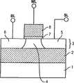
图1显示传统的浮体DRAM(动态随机存取存储器)存储器单元的剖视图。FIG. 1 shows a cross-sectional view of a conventional floating body DRAM (Dynamic Random Access Memory) memory cell.
传统的浮体DRAM单元形成在包括硅薄膜3的绝缘体上硅(SOI)衬底中,硅薄膜3通过埋入氧化物层(BOX)2与基衬底1分开。浮体4、源极区5和漏极区6形成在BOX 2上的薄膜3中。栅极介电层7和栅极电极8顺序设置在浮体4上方。漏极区6连接到位线BL,源极区5连接到源极线(source line)SL,栅极电极8连接到字线(wordline)WL。A conventional floating body DRAM cell is formed in a silicon-on-insulator (SOI) substrate including a silicon
浮体通过BOX、栅极介电层、源极区和漏极区电绝缘。由于绝缘,浮体可以存储电荷。The floating body is electrically insulated by the BOX, the gate dielectric layer, the source region and the drain region. Due to the insulation, the floating body can store charge.
在晶体管中的数据写入操作中,浮体利用碰撞电离现象来存储电荷,这修改了晶体管的阈值电压。这样,在数据读取操作中,流过晶体管的源极和漏极之间的电流量取决于存储在浮体中的电荷量。During data writing operations in transistors, the floating body uses the phenomenon of impact ionization to store charge, which modifies the threshold voltage of the transistor. Thus, in a data read operation, the amount of current flowing between the source and drain of the transistor depends on the amount of charge stored in the floating body.
为了能够执行逻辑1状态写入操作(在下文中该操作被称为“WRITE 1”),大约为施加到栅极电极的额定电源电压VDD的2.5倍的较高电压必须被施加到位线BL。该高电压除了可能损坏单元以外,还可能破坏附近的存储器单元的操作。产生该高电压还需要专用的电路来作为电荷泵。In order to be able to perform a
在文献US 2004/0108532中描述了一种用于减小浮体DRAM存储器单元所占据的表面积的技术。该文献提出通过连接浮体水平FET晶体管和适于将电荷注入浮体中的水平双极型晶体管来制造存储器单元。从而增大浮体的较低的存储电容。A technique for reducing the surface area occupied by a floating body DRAM memory cell is described in document US 2004/0108532. This document proposes to fabricate a memory cell by connecting a floating body horizontal FET transistor and a horizontal bipolar transistor adapted to inject charge into the floating body. This increases the lower storage capacitance of the floating body.
横向于FET晶体管特别设置水平双极型晶体管,其中双极型晶体管的发射极(作为注入器,injector)形成在与双极型晶体管具有相反导电性的衬底中,双极型晶体管的基极由衬底形成,双极型晶体管的集电极作为FET晶体管的浮体。Horizontal bipolar transistors are especially arranged laterally to the FET transistors, wherein the emitter of the bipolar transistor (as an injector, injector) is formed in a substrate having the opposite conductivity to that of the bipolar transistor, and the base of the bipolar transistor Formed from the substrate, the collector of the bipolar transistor acts as the floating body of the FET transistor.
通过这种结构,存储器单元的表面积被减小到大约10F2。但是,在这种结构中,发射极和基极占用表面积,从而本领域技术人员仍希望进一步减小存储器单元的表面积。With this structure, the surface area of the memory cell is reduced to about 10F2 . However, in this structure, the emitter and the base occupy surface area, so those skilled in the art still desire to further reduce the surface area of the memory cell.
此外,该存储器单元的缺点是难以准确地控制作为双极型晶体管的基极的衬底的电压。此外,由于注入器由两个相邻的存储器单元共享,因此存在这些相邻单元之间出现干扰的风险。Furthermore, the memory cell has a disadvantage in that it is difficult to accurately control the voltage of the substrate which is the base of the bipolar transistor. Furthermore, since the injector is shared by two adjacent memory cells, there is a risk of interference between these adjacent cells.
因此可以理解,根据文献US 2004/0108532的存储器单元并不完全令人满意,仍需要弥补现有技术中的上述缺陷。It can therefore be understood that the memory cell according to document US 2004/0108532 is not entirely satisfactory and that there is still a need to remedy the above-mentioned drawbacks of the prior art.
发明内容Contents of the invention
本发明的目的是提出一种具有减小的表面积的改进的存储器单元。为此,根据第一方面,本发明提出一种存储器单元,包括:It is an object of the present invention to propose an improved memory cell with reduced surface area. Therefore, according to the first aspect, the present invention proposes a memory unit, comprising:
具有源极、漏极和位于源极和漏极之间的浮体的FET晶体管,A FET transistor having a source, a drain, and a floating body between the source and drain,
可以被控制为将电荷注入FET晶体管的浮体中的注入器(injector),所述注入器包括双极型晶体管,所述双极型晶体管具有发射极、基极和由FET晶体管的浮体形成的集电极,An injector that can be controlled to inject charge into the floating body of a FET transistor, the injector comprising a bipolar transistor having an emitter, a base, and a collector formed by the floating body of the FET transistor electrode,
所述单元的特征在于,双极型晶体管的发射极被设置为FET晶体管的源极作为双极型晶体管的基极。The cell is characterized in that the emitter of the bipolar transistor is arranged as the source of the FET transistor as the base of the bipolar transistor.
该存储器单元的一些优选的非限制的方面如下所述:Some preferred non-limiting aspects of the memory unit are as follows:
FET晶体管是水平的,发射极被设置为发射极/源极组件形成垂直堆叠;FET transistors are horizontal and emitters are arranged as emitter/source assemblies forming a vertical stack;
发射极连接到在单元的表面下方延伸的注入线;The emitter is connected to an injection line extending below the surface of the cell;
发射极结合到源极中;The emitter is incorporated into the source;
发射极设置在源极的底部区域中;the emitter is arranged in the bottom region of the source;
源极包括强掺杂中心区和围绕所述中心区的弱掺杂边缘区,发射极设置在源极的边缘区中,在源极的中心区下方;The source electrode comprises a strongly doped central region and a weakly doped edge region surrounding said central region, the emitter being arranged in the edge region of the source, below the central region of the source;
发射极设置在源极的顶部区域中;the emitter is arranged in the top region of the source;
源极包括弱掺杂顶部区域和设置在顶部区域下的强掺杂底部区域,发射极结合在顶部区域中;The source comprises a weakly doped top region and a strongly doped bottom region disposed below the top region, the emitter being incorporated in the top region;
源极的底部区域设置在埋入绝缘层下方,并通过延伸穿过绝缘层的连接通道连接到源极的顶部区域;a bottom region of the source is disposed below the buried insulating layer and connected to a top region of the source by a connecting channel extending through the insulating layer;
发射极设置在源极下方;The emitter is arranged below the source;
发射极设置埋入绝缘层下方,并通过延伸穿过绝缘层的连接通道连接到源极;The emitter is arranged buried under the insulating layer and connected to the source through a connecting channel extending through the insulating layer;
FET晶体管还包括凹入在浮体中并通过介电层与浮体绝缘的栅极电极;The FET transistor also includes a gate electrode recessed in the floating body and insulated from the floating body by a dielectric layer;
发射极包括导电性与源极的导电性相反的掺杂半导体材料;the emitter comprises a doped semiconductor material having a conductivity opposite to that of the source;
所述单元制造在绝缘体上半导体衬底上;The unit is fabricated on a semiconductor-on-insulator substrate;
FET晶体管形成在井(well)中,井制造在体衬底的顶部中。FET transistors are formed in wells fabricated in the top of the bulk substrate.
根据另一方面,本发明涉及一种存储器单元,包括:According to another aspect, the invention relates to a memory cell comprising:
具有源极、漏极和位于源极和漏极之间的浮体的FET晶体管,A FET transistor having a source, a drain, and a floating body between the source and drain,
可以被控制为将电荷注入FET晶体管的浮体中的注入器(injector),所述注入器包括双极型晶体管,所述双极型晶体管具有发射极、基极和由FET晶体管的浮体形成的集电极,An injector that can be controlled to inject charge into the floating body of a FET transistor, the injector comprising a bipolar transistor having an emitter, a base, and a collector formed by the floating body of the FET transistor electrode,
所述单元的特征在于,发射极连接到在单元的表面下方延伸的注入线。The cell is characterized in that the emitter is connected to an injection line extending below the surface of the cell.
根据另一方面,本发明涉及包括多个根据本发明的第一方面的存储器单元的存储器阵列。According to another aspect, the invention relates to a memory array comprising a plurality of memory cells according to the first aspect of the invention.
特别地,存储器阵列可以包括耦合到沿着阵列的列的每个存储器单元的源极的源极线,以及平行于源极线的耦合到沿着所述列的每个存储器单元的发射极的注入线。In particular, a memory array may include a source line coupled to the source of each memory cell along a column of the array, and a line parallel to the source line coupled to the emitter of each memory cell along the column. Inject line.
根据再一方面,本发明涉及一种编程存储器单元的方法,所述存储器单元包括具有浮体的水平FET晶体管和可以被控制为将电荷注入FET晶体管的浮体中的注入器,其特征在于,通过向FET晶体管的栅极施加额定写入电压,通过向FET晶体管的漏极施加小于或等于额定写入电压的电压以及通过向注入器施加正电压来编程逻辑1状态。According to yet another aspect, the present invention relates to a method of programming a memory cell comprising a horizontal FET transistor with a floating body and an injector controllable to inject charge into the floating body of the FET transistor, characterized in that by feeding A
在单元读取操作中,还可以向FET晶体管的栅极施加额定写入电压的一部分。In a cell read operation, a fraction of the nominal write voltage may also be applied to the gate of the FET transistor.
附图说明Description of drawings
通过阅读以非限制示例以及参考附图给出的本发明的优选实施例的以下详细描述,本发明的其他方面、目的和优点将更明显,其中:Other aspects, objects and advantages of the invention will become more apparent by reading the following detailed description of preferred embodiments of the invention given by way of non-limiting examples and with reference to the accompanying drawings, in which:
如前所述,图1显示传统的浮体DRAM单元;As mentioned earlier, Figure 1 shows a conventional floating body DRAM cell;
图2a显示根据本发明的第一方面的一个可能实施例的存储器单元的剖视图;Figure 2a shows a cross-sectional view of a memory cell according to a possible embodiment of the first aspect of the invention;
图2b显示利用图2a的存储器单元的存储器阵列的可能拓扑;Figure 2b shows a possible topology of a memory array utilizing the memory cells of Figure 2a;
图2c显示等效于图2a的存储器单元的电路图;Figure 2c shows a circuit diagram equivalent to the memory cell of Figure 2a;
图3a显示根据本发明的可能实施例的在绝缘体上半导体衬底上使用部分耗尽的FET晶体管的存储器单元;Figure 3a shows a memory cell using a partially depleted FET transistor on a semiconductor-on-insulator substrate according to a possible embodiment of the invention;
图3b显示根据本发明的可能实施例的在体衬底上使用FET晶体管的存储器单元;Figure 3b shows a memory cell using FET transistors on a bulk substrate according to a possible embodiment of the invention;
图3c显示根据本发明的存储器单元的另一个可能实施例,其中注入线埋入绝缘层下方;Figure 3c shows another possible embodiment of a memory cell according to the invention, wherein the implant line is buried under the insulating layer;
图3d显示根据本发明的存储器单元的另一个可能实施例,其中源极线埋入绝缘层下方;Figure 3d shows another possible embodiment of a memory cell according to the invention, wherein the source line is buried under the insulating layer;
图3e显示利用图3d的存储器单元的存储器阵列的可能拓扑;Figure 3e shows a possible topology of a memory array utilizing the memory cells of Figure 3d;
图4a和4b分别显示基于等效电路图的在传统的DRAM单元和根据本发明的DRAM单元中编程逻辑0状态的操作;Figures 4a and 4b show the operation of programming a logic 0 state in a conventional DRAM cell and a DRAM cell according to the present invention, respectively, based on an equivalent circuit diagram;
图5a和5b分别显示基于等效电路图的在传统的DRAM单元和根据本发明的DRAM单元中编程逻辑1状态的操作;Figures 5a and 5b show the operation of programming a
图6a和6b分别显示基于等效电路图的存储在传统的DRAM单元和根据本发明的DRAM单元中读取逻辑状态的操作;Figures 6a and 6b respectively show the operation of reading logic states stored in a traditional DRAM cell and a DRAM cell according to the present invention based on an equivalent circuit diagram;
图7a和7b分别显示基于等效电路图的存储在传统的DRAM单元和根据本发明的DRAM单元中保持逻辑状态的操作;Figures 7a and 7b respectively show the operation of storing logic states based on equivalent circuit diagrams in a conventional DRAM cell and in a DRAM cell according to the present invention;
图8显示利用根据本发明的存储器单元的存储器阵列的另一个可能拓扑。Figure 8 shows another possible topology of a memory array utilizing memory cells according to the invention.
具体实施方式Detailed ways
参考图2a,显示了根据本发明的第一方面的优选实施例的存储器单元的剖视图。该单元包括FET晶体管,FET晶体管具有源极S、漏极D和源极与漏极之间的浮体FB,以及被控制为将电荷注入FET晶体管的浮体FB中的注入器(injector)。Referring to Figure 2a, there is shown a cross-sectional view of a memory cell according to a preferred embodiment of the first aspect of the present invention. The cell comprises an FET transistor having a source S, a drain D and a floating body FB between the source and the drain, and an injector controlled to inject charge into the floating body FB of the FET transistor.
在这种情况下,存储器单元制造在绝缘体上半导体SeOI衬底上,优选地是绝缘体上硅SOI衬底。In this case, the memory cells are fabricated on a semiconductor-on-insulator SeOI substrate, preferably a silicon-on-insulator SOI substrate.
漏极D和源极S优选地接触埋入氧化物层BOX,从而FET晶体管完全耗尽。The drain D and source S preferably contact the buried oxide layer BOX so that the FET transistor is fully depleted.
两个相邻的存储器单元(沿着在图2a的平面中延伸的存储器阵列的行;垂直于图2a的平面延伸的存储器阵列的列)之间可以共享源极S。这种共享可以减小存储器单元占据的表面积。The source S may be shared between two adjacent memory cells (along a row of the memory array extending in the plane of FIG. 2a; a column of the memory array extending perpendicular to the plane of FIG. 2a). This sharing can reduce the surface area occupied by the memory cells.
但是如图3a和3b可见,本发明并不限于完全耗尽的存储器单元,还扩展到部分耗尽的SeOI上的存储器单元(图3a)和体衬底上的存储器单元(图3b)。But as can be seen in Figures 3a and 3b, the invention is not limited to fully depleted memory cells, but also extends to memory cells on partially depleted SeOI (Figure 3a) and on bulk substrates (Figure 3b).
在图3a和3b的情况下,通过现有技术中已知的方式,需要沿着存储器单元的行隔离单元,以便产生浮体效应。In the case of Figures 3a and 3b, the cells need to be isolated along the row of memory cells in order to create the floating body effect, by means known in the prior art.
在图3a的情况下,通常通过横向隔离沿深度方向从衬底表面延伸到BOX的沟槽13来实现上述隔离(根据浅沟槽隔离STI技术)。In the case of Fig. 3a, the above-mentioned isolation is generally achieved by lateral isolation (according to Shallow Trench Isolation STI technology) of the
在图3b的情况下,通常通过以下方式来实现上述隔离:横向隔离沿深度方向从衬底表面延伸的沟槽14,以及隔离体衬底的顶部中产生的并被沟槽14划界的井(well)15中的存储器单元。FET晶体管位于半导体井15中,其导电性与通道相同,从而可以将其与衬底隔离。井还可以设置在具有相反导电性(opposite conductivity)的衬底的层16中。In the case of Figure 3b, the isolation described above is generally achieved by laterally isolating
返回图2a,注入器包括具有发射极15、基极和由FET晶体管的浮体FB形成的集电极的双极型晶体管。Returning to Figure 2a, the injector comprises a bipolar transistor having an
在本发明的上下文中,双极型晶体管的发射极15被设置为FET晶体管的源极S作为双极型晶体管的基极。应注意,控制作为双极型晶体管的基极的源极的电压比控制作为文献US 2004/0108532中描述的存储器单元的双极型晶体管的基极的衬底的电压更容易。In the context of the present invention, the
FET晶体管是水平晶体管,双极型晶体管的发射极特别设置为面对FET晶体管的源极,从而发射极/源极组合形成垂直堆叠。FET transistors are horizontal transistors, and bipolar transistors have their emitters specifically positioned to face the source of the FET transistor so that the emitter/source combination forms a vertical stack.
在优选实施例中,发射极连接到在存储器单元的表面下方延伸的注入线,从而不占用表面积。In a preferred embodiment, the emitter is connected to an implant line that extends below the surface of the memory cell so that no surface area is taken up.
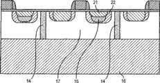
双极型晶体管的发射极15特别可以结合在FET晶体管的源极中。根据图2a所示的第一变化实施例,发射极15结合到源极21和22的底部区域中。根据图3d所示的第二变化实施例,发射极35结合到源极31和32的顶部区域中。The
参考图2a,源极通常以已知方式包括强掺杂中心区21(例如N+)和环绕中心区的弱掺杂边缘区22(例如N-)。强掺杂中心区21的主要目的是保证与源极线SL的接触,而弱掺杂边缘区22主要便于FET晶体管的操作。因此,在本发明的上下文中,使用弱掺杂区22作为双极型晶体管的基极。Referring to Figure 2a, the source generally comprises in a known manner a strongly doped central region 21 (eg N+) and a weakly doped edge region 22 (eg N-) surrounding the central region. The main purpose of the strongly doped
在该变化例的上下文中,发射极15被设置为位于源极的中心区21下方,同时与源极的边缘区22接触并通过源极的边缘22与浮体FB隔离。在这种情况下,发射极整体结合在中心区21和边缘区22之间的源极电极中。In the context of this variant, the
在存储器单元由完全耗尽的SeOI制成的情况下(见图2a),与存储器单元由部分耗尽的SeOI(图3a)或者体衬底上的存储器单元(图3b)制成的情况不同,BOX有助于隔离发射极15和浮体。In the case of memory cells made of fully depleted SeOI (see Figure 2a), as opposed to memory cells made of partially depleted SeOI (Figure 3a) or memory cells on bulk substrates (Figure 3b) , BOX helps to isolate the
应注意,漏极D也可以具有强掺杂中心区11(例如N+)和环绕中心区的弱掺杂边缘区12(例如N-)。It should be noted that the drain D may also have a strongly doped central region 11 (eg N+) and a weakly doped edge region 12 (eg N−) surrounding the central region.
通过现有技术中已知的方式,漏极D连接到位线BL。位线BL可以沿着存储器阵列的行延伸,与沿着该行设置的每个存储器单元的漏极接触。The drain D is connected to the bit line BL by means known in the art. A bit line BL may extend along a row of the memory array, contacting the drain of each memory cell disposed along the row.
如图2b可见,源极S连接到源极线SL。源极线SL通常垂直于位线BL延伸,与沿着存储器阵列的列设置的每个存储器单元的源极(通常是源极的强掺杂区)接触。As can be seen in Figure 2b, the source S is connected to the source line SL. A source line SL extends generally perpendicular to the bit lines BL, contacting the source (typically a heavily doped region of the source) of each memory cell disposed along the column of the memory array.
在图2a和2b的情况下,因此源极线SL直接在SeOI衬底的表面下方延伸。In the case of Figures 2a and 2b, the source line SL therefore extends directly below the surface of the SeOI substrate.
此外,在图2a和2b的情况下,在两个相邻单元之间共享源极,一根源极线SL可用于两个存储器单元的源极编址(address)。Furthermore, in the case of Figures 2a and 2b, where the source is shared between two adjacent cells, one source line SL can be used for source addressing of both memory cells.
发射极15连接到平行于源极线SL延伸的注入线IL,从而对沿着存储器阵列的列设置的存储器单元编址(address)。The
通过以上描述可以理解,在图2a的情况下,注入线IL设置在源极线SL下方。因此注入线IL的这种特别紧凑的结构不占用任何表面区域。It can be understood from the above description that in the case of FIG. 2a, the injection line IL is disposed below the source line SL. This particularly compact structure of the injection line IL therefore does not occupy any surface area.
图2b显示根据本发明的存储器阵列的拓扑,其中两个相邻单元之间共享源极线SL。这种结构更为紧凑。Figure 2b shows the topology of a memory array according to the present invention, where the source line SL is shared between two adjacent cells. This structure is more compact.
根据图2b的拓扑,在开发独立存储器的情况下,存储器单元的表面积可以被减小到大约4F2。虽然该单元并不是对干扰完全不敏感,但是干扰的水平低,而且在任何情况下均低于传统的存储器单元中出现的干扰水平。According to the topology of Fig. 2b, the surface area of the memory cell can be reduced to about4F2 in the case of developing a stand-alone memory. Although the cell is not completely insensitive to disturbances, the level of disturbances is low and in any case lower than that found in conventional memory cells.
在嵌入存储器的情况下,如果晶体管的要求较高(需要设置隔离件以避免交叉励磁现象),晶体管占据的表面积较大。则获得的存储器单元的表面积在15F2到18F2的数量级。但是,其具有对干扰完全不敏感的优点。In the case of embedded memories, if the requirements on the transistors are high (spacers are required to avoid cross-excitation phenomena), the surface area occupied by the transistors is large. The surface area of the resulting memory cell is then on the order of 15F2 to 18F2 . However, it has the advantage of being completely insensitive to interference.
图8显示了另一种可能的拓扑,其紧凑性较差但是对干扰完全不敏感。在这种拓扑中,字线WL控制共享公共源极线SL的两个相邻的物理行。这种特别结构消除了大部分的源极相互干扰,因为位于双字线WL上的单元全被使用,而且可以合理地推断写入电路比干扰更强。另一方面,彼此上下设置的两个单元必须强制连接到两条不同的位线BL1和BL2,否则在访问WL的过程中它们的信息可能混合。这直接影响单元的表面积,因为必须足够宽以便容纳彼此并排的两根金属线。虽然对于独立存储器而言通常禁止彼此并排的两根金属线,但是在另一方面,在嵌入存储器的情况下,其非常合理地将单元的表面积限制在大约4F*4F=16F2。Figure 8 shows another possible topology that is less compact but completely insensitive to interference. In this topology, a word line WL controls two adjacent physical rows that share a common source line SL. This particular configuration eliminates most of the source-to-source interference, since the cells on the double word line WL are all used, and it is reasonable to infer that the write circuit is stronger than the interference. On the other hand, two cells placed one above the other must be forced to be connected to two different bit lines BL1 and BL2, otherwise their information may be mixed during access to WL. This directly affects the surface area of the cell, as it must be wide enough to accommodate the two wires alongside each other. While two metal lines next to each other are generally forbidden for stand-alone memories, on the other hand, in the case of embedded memories, it very reasonably limits the surface area of the cell to about 4F*4F=16F2 .
如图2a所示,FET晶体管还具有位于浮体上方、存储器阵列的表面上并且通过介电层与浮体绝缘的栅极电极。栅极电极连接到通常沿着存储器阵列的列延伸的字线WL。As shown in Figure 2a, the FET transistor also has a gate electrode located above the floating body, on the surface of the memory array and insulated from the floating body by a dielectric layer. The gate electrodes are connected to word lines WL that generally run along the columns of the memory array.
根据未显示的另一个实施例,栅极电极在浮体中凹入,并且通过介电层与浮体绝缘。由此定义了RCAT(凹槽阵列晶体管)型晶体管。According to another embodiment not shown, the gate electrode is recessed in the floating body and is insulated from the floating body by a dielectric layer. RCAT (Recess Array Transistor) type transistors are thus defined.
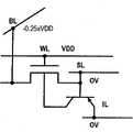
图2c是等效于根据本发明的第一方面的存储器单元的电路图。在图中,FET晶体管(在本例中是N型晶体管)的附图标记是9,双极型晶体管(在本例中是PNP型晶体管)的附图标记是10。如上所述,连接到源极线SL的FET晶体管9的源极作为双极型晶体管10的基极,而FET晶体管9的浮体作为双极型晶体管10的集电极。Figure 2c is a circuit diagram equivalent to a memory cell according to the first aspect of the invention. In the drawing, a FET transistor (N-type transistor in this example) is referenced at 9 , and a bipolar transistor (PNP-type transistor in this example) is referenced at 10 . As mentioned above, the source of the FET transistor 9 connected to the source line SL acts as the base of the
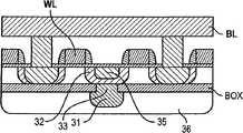
参考图3d,其显示了另一个变化实施例,发射极35结合在源极31和32的顶部区域中。Referring to FIG. 3 d , which shows another variant embodiment, the
在该变化例的上下文中,源极S包括弱掺杂顶部区域32和设置在顶部区域下方的强掺杂底部区域31,发射极35结合在顶部区域32中。In the context of this variant, the source S comprises a weakly doped
如图3d所示,源极的底部区域31特别设置在衬底中的埋入绝缘层下方,例如对于SeOI衬底的情况是BOX层,同时通过延伸穿过绝缘层的连接通道33连接到源极的顶部区域32。As shown in Figure 3d, the
源极的强掺杂底部区域31(在所述示例中是N+掺杂)特别设置在绝缘层下方的具有相反导电性的衬底区域(在所述实例中是P-区域)36中。A heavily doped
在该变化例的上下文中,埋入源极线SL;其特别可以直接埋入绝缘层BOX下方,如图3d所示。双极型晶体管的发射极35连接到直接在衬底的表面下延伸并因此更容易接近(access)的注入线IL(代替传统单元的源极线而设置该注入线IL)。此外,在该变化例中,源极和发射极的垂直堆叠具有注入线不占用表面积的特别效果。In the context of this variant, the source line SL is buried; it may in particular be buried directly under the insulating layer BOX, as shown in FIG. 3d. The
图3e显示利用图3d的存储器单元的存储器阵列的可能拓扑。在该拓扑中,源极线SL沿着存储器阵列的列平行于注入线IL延伸,同时埋入注入线下方,BOX层下。在该变化实施例中,容易接近注入线IL。Figure 3e shows a possible topology of a memory array utilizing the memory cells of Figure 3d. In this topology, the source lines SL run parallel to the implant lines IL along the columns of the memory array, while being buried below the implant lines, below the BOX layer. In this variant embodiment, the injection line IL is easily accessible.
图3c显示另一个可能实施例,其中通过在源极21和22下方设置发射极25而获得源极和发射极的垂直堆叠。应注意,该实施例对应于图3d的变化例,其中发射极和源极的强掺杂区域简单互换。Fig. 3c shows another possible embodiment, where a vertical stack of sources and emitters is obtained by arranging
实际上,在其他实施例中,发射极25(P+)埋入绝缘层下具有相反导电性(在本例中是N-)的衬底区域26中,并通过延伸穿过绝缘层的连接通道23连接到源极的边缘区域22。Indeed, in other embodiments, the emitter 25 (P+) is buried in a
通常,源极线SL直接在衬底表面下延伸,而注入线IL在BOX层下平行于源极线SL延伸。因此,注入线IL不占用任何表面积。Typically, the source line SL runs directly under the substrate surface, while the implant line IL runs parallel to the source line SL under the BOX layer. Therefore, the injection line IL does not occupy any surface area.
根据本发明说明书的以上描述,注入线优选地利用掺杂的半导体材料制成。在图中所示的FET晶体管是N型(P型浮体)的例子中,掺杂半导体材料是衬底材料的P型掺杂(特别地,P+掺杂)。可以理解,本发明不限于N型FET晶体管,还可以扩展到P型FET晶体管(N型浮体)的情况。According to the above description of the present specification, the injection line is preferably made of a doped semiconductor material. In the example shown in the figure where the FET transistor is N-type (P-type floating body), the doped semiconductor material is a P-type doping (in particular, P+ doping) of the substrate material. It can be understood that the present invention is not limited to N-type FET transistors, but can also be extended to the case of P-type FET transistors (N-type floating body).
通过使用CMOS技术中常用的技术,制造衬底掺杂从而制造注入线IL,注入线IL不需要金属化从而可以避免金属配线。By using techniques commonly used in CMOS technology, the substrate is doped to create the implant line IL, which does not require metallization so that metal wiring can be avoided.
图4a-4b,5a-5b,6a-6b和7a-7b显示图2a的等效电路图,以便比较图1所示的传统类型的存储器单元(图4a、5a、6a和7a)与根据本发明的存储器单元(图4b、5b、6b和7b)的不同编程、读取和保持(hold)操作。Figures 4a-4b, 5a-5b, 6a-6b and 7a-7b show the equivalent circuit diagram of Figure 2a in order to compare the memory cell of the conventional type shown in Figure 1 (Figures 4a, 5a, 6a and 7a) with those according to the present invention Different programming, reading and holding (hold) operations of the memory cells (Figures 4b, 5b, 6b and 7b).
在各个附图中:In the various drawings:
图4a和4b显示用于编程逻辑0状态的WRITE 0操作,Figures 4a and 4b show a WRITE 0 operation for programming a logic 0 state,
图5a和5b显示用于编程逻辑1状态的WRITE 1操作,Figures 5a and 5b show a
图6a和6b显示用于读取逻辑状态的READ操作,Figures 6a and 6b show the READ operation for reading the logic state,
图7a和7b显示用于保持逻辑状态的HOLD操作。Figures 7a and 7b show the HOLD operation used to hold logic states.
下表显示控制这些单元并执行这些不同操作而必须施加到不同的线上的电压示例。The table below shows examples of the voltages that must be applied to the different lines to control these units and perform these different operations.
表1图1的存储器单元Table 1 Memory cells of Figure 1
表2根据本发明的存储器单元Table 2 Memory cells according to the present invention
首先可以观察到,用于执行读取操作READ而施加到字线WL的电压被降低到额定电源电压VDD的一小部分,例如0.5VDD。这可以降低单元的整体耗电水平。此外,因为该电压位于两个阈值电压水平(“0”和“1”)之间,读取选择导致对于最低阈值电压(原则上,通常是“0”)存在电流,而在其他情况下不存在电流。此外,检测放大器的设计被简化为“简单的”比较器,该“简单的”比较器比必须将具有不同大小的两个电流与参考值比较的情况更容易设计,所述参考值必须是已知并被信任的。It can first be observed that the voltage applied to the word line WL for performing the read operation READ is reduced to a fraction of the nominal supply voltage VDD, eg 0.5 VDD. This reduces the overall power consumption level of the unit. Furthermore, since this voltage lies between two threshold voltage levels ("0" and "1"), read selection results in a current being present for the lowest threshold voltage (in principle, usually "0") and not otherwise. There is an electric current. Furthermore, the design of the sense amplifier is reduced to a "simple" comparator which is easier to design than if two currents with different magnitudes had to be compared to a reference value which had to be known and trusted.
此外,如在背景技术部分描述的,大约为额定写入电压VDD的2.5倍的电压必须被施加到传统存储器单元的漏极以便执行WRITE 1操作。Furthermore, as described in the Background Art section, a voltage approximately 2.5 times the rated write voltage VDD must be applied to the drain of a conventional memory cell in order to perform a
通过使用注入器将电荷注入浮体中,本发明能够降低执行WRITE1操作所需的电压。特别地,需要施加到根据本发明的存储器单元的漏极的电压小于或等于额定电压VDD,例如在上表2中所示,等于0.75VDD。By injecting charge into the floating body using an injector, the present invention can reduce the voltage required to perform the WRITE1 operation. In particular, it is required that the voltage applied to the drain of the memory cell according to the present invention be less than or equal to the rated voltage VDD, eg equal to 0.75 VDD as indicated in Table 2 above.
以施加到所有电源线1的低电压来执行所有编程操作具有几个优点。Performing all programming operations with a low voltage applied to all
首先,降低功率消耗,并简化外围电路设计。特别地,不需要产生高压(特别对于WRITE 1操作,对于传统的存储器单元为2.5VDD)的电路。First, reduce power consumption and simplify peripheral circuit design. In particular, no circuitry is required to generate high voltages (especially for
此外,通过降低电压,避免存储器单元的损坏。还避免相邻单元之间的干扰。Furthermore, by lowering the voltage, damage to the memory cells is avoided. Interference between adjacent cells is also avoided.
因此,在所述示例中,在写入操作中可能由位线BL产生的对相邻单元的干扰对应于正被讨论的示例中的位线BL上的0.75VDD(WRITE1)或者-0.25VDD(WRITE 0)的电压(WL=SL=IL=0V)。这些较低电压不易产生明显干扰。Thus, in the example in question, the disturbance to neighboring cells that may be produced by the bit line BL during a write operation corresponds to 0.75 VDD (WRITE1) or -0.25 VDD ( WRITE 0) voltage (WL=SL=IL=0V). These lower voltages are less prone to significant interference.
在WRITE 1写入操作中可能由字线WL产生的对相邻单元的干扰对应于字线WL上的VDD和注入线IL上的0.75VDD的各自电压(并且BL=SL=0V)。因此容易出现通过双极型晶体管将电荷(在这里描述的示例中是空穴)注入浮体中。The disturbance to adjacent cells that may be generated by word line WL in a
在相邻单元的WRITE 0写入操作中,WL为VDD,而BL=SL=IL=0V。然后双极型晶体管(在所述示例中为PNP型)关闭,通过负的位线所有空穴可以被排空。In the WRITE 0 write operation of adjacent cells, WL is VDD, and BL=SL=IL=0V. The bipolar transistor (PNP type in the example) is then turned off and all holes can be evacuated through the negative bit line.
为了简单地克服这些干扰现象,如果单元位于有源位线WL上,可以选择写入强调的单元(stressed cell)而不保持无源(这等效于通过在所有相应的位线上施加适当的电压沿着WL在所有单元上执行有效的WRITE操作)。这以分离存储器作为条件(要求沿着字线WL的所有单元属于相同的字),但是如果所有所述强调的单元可以直接被该应用使用,则不引起任何问题。实际上,如果字较宽,信息比特率较大以及最终耗电较低。To simply overcome these disturbance phenomena, one can choose to write a stressed cell without remaining passive if the cell is on an active bit line WL (this is equivalent to applying the appropriate voltage along WL to perform an effective WRITE operation on all cells). This is conditional on splitting the memory (requiring that all cells along the word line WL belong to the same word), but does not cause any problems if all said highlighted cells can be directly used by the application. In fact, if the word is wider, the information bit rate is higher and the final power consumption is lower.
通过以上描述可以理解,本发明不限于根据本发明的第一方面的存储器单元,本发明还扩展到包括多个根据本发明的第一方面的存储器单元的存储器阵列,以及控制这种存储器单元的方法。As can be understood from the above description, the present invention is not limited to the memory unit according to the first aspect of the present invention, and the present invention also extends to a memory array comprising a plurality of memory units according to the first aspect of the present invention, and a method for controlling such a memory unit method.
Claims (19)
Translated fromChineseApplications Claiming Priority (2)
| Application Number | Priority Date | Filing Date | Title |
|---|---|---|---|
| FR1050241 | 2010-01-14 | ||
| FR1050241AFR2955204B1 (en) | 2010-01-14 | 2010-01-14 | DRAM MEMORY CELL HAVING A VERTICAL BIPOLAR INJECTOR |
Publications (2)
| Publication Number | Publication Date |
|---|---|
| CN102130128Atrue CN102130128A (en) | 2011-07-20 |
| CN102130128B CN102130128B (en) | 2014-01-08 |
Family
ID=42289816
Family Applications (1)
| Application Number | Title | Priority Date | Filing Date |
|---|---|---|---|
| CN201010521914.4AActiveCN102130128B (en) | 2010-01-14 | 2010-10-25 | DRAM memory cell with vertical bipolar injector |
Country Status (8)
| Country | Link |
|---|---|
| US (1) | US8305803B2 (en) |
| EP (1) | EP2346077A1 (en) |
| JP (1) | JP5420517B2 (en) |
| KR (1) | KR101135826B1 (en) |
| CN (1) | CN102130128B (en) |
| FR (1) | FR2955204B1 (en) |
| SG (1) | SG173247A1 (en) |
| TW (1) | TWI470771B (en) |
Cited By (1)
| Publication number | Priority date | Publication date | Assignee | Title |
|---|---|---|---|---|
| CN109599439A (en)* | 2017-12-28 | 2019-04-09 | 新唐科技股份有限公司 | Transverse diffusion metal oxide semiconductor field effect transistor |
Families Citing this family (8)
| Publication number | Priority date | Publication date | Assignee | Title |
|---|---|---|---|---|
| US8547756B2 (en) | 2010-10-04 | 2013-10-01 | Zeno Semiconductor, Inc. | Semiconductor memory device having an electrically floating body transistor |
| US8130547B2 (en) | 2007-11-29 | 2012-03-06 | Zeno Semiconductor, Inc. | Method of maintaining the state of semiconductor memory having electrically floating body transistor |
| FR2955200B1 (en)* | 2010-01-14 | 2012-07-20 | Soitec Silicon On Insulator | DEVICE AND MANUFACTURING METHOD HAVING CONTACT BETWEEN SEMICONDUCTOR REGIONS THROUGH AN INSULATED INSULATED LAYER |
| US10340276B2 (en) | 2010-03-02 | 2019-07-02 | Zeno Semiconductor, Inc. | Method of maintaining the state of semiconductor memory having electrically floating body transistor |
| KR102084954B1 (en) | 2013-05-02 | 2020-03-05 | 삼성전자주식회사 | Semiconductor device and method of fabricating the same |
| US9281022B2 (en)* | 2013-07-10 | 2016-03-08 | Zeno Semiconductor, Inc. | Systems and methods for reducing standby power in floating body memory devices |
| US9548119B2 (en) | 2014-01-15 | 2017-01-17 | Zeno Semiconductor, Inc | Memory device comprising an electrically floating body transistor |
| US9331097B2 (en) | 2014-03-03 | 2016-05-03 | International Business Machines Corporation | High speed bipolar junction transistor for high voltage applications |
Citations (4)
| Publication number | Priority date | Publication date | Assignee | Title |
|---|---|---|---|---|
| CN1744321A (en)* | 2004-08-31 | 2006-03-08 | 株式会社东芝 | Semiconductor integrated device |
| US20060226463A1 (en)* | 2002-08-29 | 2006-10-12 | Micron Technology, Inc. | Merged MOS-bipolar capacitor memory cell |
| CN1897282A (en)* | 2005-06-30 | 2007-01-17 | St微电子克鲁勒斯图股份公司 | Memory cell with an isolated-body mos transistor with reinforced memory effect |
| US7301195B2 (en)* | 2004-02-02 | 2007-11-27 | Kabushiki Kaisha Toshiba | Semiconductor memory device for storing data as state of majority carriers accumulated in channel body and method of manufacturing the same |
Family Cites Families (101)
| Publication number | Priority date | Publication date | Assignee | Title |
|---|---|---|---|---|
| US4169233A (en) | 1978-02-24 | 1979-09-25 | Rockwell International Corporation | High performance CMOS sense amplifier |
| KR100213602B1 (en) | 1988-05-13 | 1999-08-02 | 가나이 쓰도무 | Dram semiconductor memory device |
| US5028810A (en) | 1989-07-13 | 1991-07-02 | Intel Corporation | Four quadrant synapse cell employing single column summing line |
| JPH04345064A (en) | 1991-05-22 | 1992-12-01 | Hitachi Ltd | Semiconductor integrated circuit device and its manufacturing method |
| JP2717740B2 (en) | 1991-08-30 | 1998-02-25 | 三菱電機株式会社 | Semiconductor integrated circuit device |
| EP0836194B1 (en) | 1992-03-30 | 2000-05-24 | Mitsubishi Denki Kabushiki Kaisha | Semiconductor device |
| US5325054A (en) | 1992-07-07 | 1994-06-28 | Texas Instruments Incorporated | Method and system for screening reliability of semiconductor circuits |
| US5306530A (en) | 1992-11-23 | 1994-04-26 | Associated Universities, Inc. | Method for producing high quality thin layer films on substrates |
| JP3488730B2 (en) | 1993-11-05 | 2004-01-19 | 株式会社ルネサステクノロジ | Semiconductor integrated circuit device |
| JP3367776B2 (en) | 1993-12-27 | 2003-01-20 | 株式会社東芝 | Semiconductor device |
| US5455791A (en) | 1994-06-01 | 1995-10-03 | Zaleski; Andrzei | Method for erasing data in EEPROM devices on SOI substrates and device therefor |
| JP3003088B2 (en) | 1994-06-10 | 2000-01-24 | 住友イートンノバ株式会社 | Ion implanter |
| JP3549602B2 (en) | 1995-01-12 | 2004-08-04 | 株式会社ルネサステクノロジ | Semiconductor storage device |
| JPH08255846A (en) | 1995-03-17 | 1996-10-01 | Nippondenso Co Ltd | Semiconductor device and manufacturing method thereof |
| JP3288554B2 (en) | 1995-05-29 | 2002-06-04 | 株式会社日立製作所 | Ion implantation apparatus and ion implantation method |
| JPH0982814A (en) | 1995-07-10 | 1997-03-28 | Denso Corp | Semiconductor integrated circuit device and manufacturing method thereof |
| US6787844B2 (en) | 1995-09-29 | 2004-09-07 | Nippon Steel Corporation | Semiconductor device including transistor with composite gate structure and transistor with single gate structure, and method for manufacturing the same |
| JP3265178B2 (en) | 1996-02-20 | 2002-03-11 | 株式会社東芝 | Semiconductor memory device and method of manufacturing the same |
| JPH10125064A (en) | 1996-10-14 | 1998-05-15 | Toshiba Corp | Storage device |
| JPH10208484A (en) | 1997-01-29 | 1998-08-07 | Mitsubishi Electric Corp | Data read circuit of semiconductor memory device and semiconductor memory device |
| US5889293A (en) | 1997-04-04 | 1999-03-30 | International Business Machines Corporation | Electrical contact to buried SOI structures |
| JP3120389B2 (en) | 1998-04-16 | 2000-12-25 | 日本電気株式会社 | Semiconductor device |
| JP3699823B2 (en) | 1998-05-19 | 2005-09-28 | 株式会社東芝 | Semiconductor device |
| US6072217A (en) | 1998-06-11 | 2000-06-06 | Sun Microsystems, Inc. | Tunable threshold SOI device using isolated well structure for back gate |
| FR2779869B1 (en) | 1998-06-15 | 2003-05-16 | Commissariat Energie Atomique | SOI-TYPE INTEGRATED CIRCUIT WITH DECOUPLING CAPABILITY, AND METHOD OF MAKING SUCH CIRCUIT |
| US6826730B2 (en) | 1998-12-15 | 2004-11-30 | Texas Instruments Incorporated | System and method for controlling current in an integrated circuit |
| JP3456913B2 (en) | 1998-12-25 | 2003-10-14 | 株式会社東芝 | Semiconductor device |
| US6372600B1 (en) | 1999-08-30 | 2002-04-16 | Agere Systems Guardian Corp. | Etch stops and alignment marks for bonded wafers |
| US6476462B2 (en) | 1999-12-28 | 2002-11-05 | Texas Instruments Incorporated | MOS-type semiconductor device and method for making same |
| US6417697B2 (en) | 2000-02-02 | 2002-07-09 | Broadcom Corporation | Circuit technique for high speed low power data transfer bus |
| US6300218B1 (en) | 2000-05-08 | 2001-10-09 | International Business Machines Corporation | Method for patterning a buried oxide thickness for a separation by implanted oxygen (simox) process |
| US6350653B1 (en) | 2000-10-12 | 2002-02-26 | International Business Machines Corporation | Embedded DRAM on silicon-on-insulator substrate |
| JP2002164544A (en) | 2000-11-28 | 2002-06-07 | Sony Corp | Semiconductor device |
| US6614190B2 (en) | 2001-01-31 | 2003-09-02 | Hitachi, Ltd. | Ion implanter |
| JP3982218B2 (en) | 2001-02-07 | 2007-09-26 | ソニー株式会社 | Semiconductor device and manufacturing method thereof |
| JP3884266B2 (en) | 2001-02-19 | 2007-02-21 | 株式会社東芝 | Semiconductor memory device and manufacturing method thereof |
| US6611023B1 (en) | 2001-05-01 | 2003-08-26 | Advanced Micro Devices, Inc. | Field effect transistor with self alligned double gate and method of forming same |
| US6759282B2 (en) | 2001-06-12 | 2004-07-06 | International Business Machines Corporation | Method and structure for buried circuits and devices |
| US6498057B1 (en) | 2002-03-07 | 2002-12-24 | International Business Machines Corporation | Method for implementing SOI transistor source connections using buried dual rail distribution |
| EP1357603A3 (en) | 2002-04-18 | 2004-01-14 | Innovative Silicon SA | Semiconductor device |
| US7710771B2 (en) | 2002-11-20 | 2010-05-04 | The Regents Of The University Of California | Method and apparatus for capacitorless double-gate storage |
| JP2004179506A (en) | 2002-11-28 | 2004-06-24 | Seiko Epson Corp | Semiconductor substrate having SOI structure, method of manufacturing the same, and semiconductor device |
| US7030436B2 (en) | 2002-12-04 | 2006-04-18 | Micron Technology, Inc. | Embedded DRAM gain memory cell having MOS transistor body provided with a bi-polar transistor charge injecting means |
| JP2004303499A (en) | 2003-03-31 | 2004-10-28 | Hitachi High-Technologies Corp | Ion implantation apparatus and ion implantation method |
| JP4077381B2 (en)* | 2003-08-29 | 2008-04-16 | 株式会社東芝 | Semiconductor integrated circuit device |
| US6965143B2 (en) | 2003-10-10 | 2005-11-15 | Advanced Micro Devices, Inc. | Recess channel flash architecture for reduced short channel effect |
| JP2005158952A (en) | 2003-11-25 | 2005-06-16 | Toshiba Corp | Semiconductor device and manufacturing method thereof |
| US7109532B1 (en)* | 2003-12-23 | 2006-09-19 | Lee Zachary K | High Ion/Ioff SOI MOSFET using body voltage control |
| US20050255666A1 (en) | 2004-05-11 | 2005-11-17 | Miradia Inc. | Method and structure for aligning mechanical based device to integrated circuits |
| US7112997B1 (en) | 2004-05-19 | 2006-09-26 | Altera Corporation | Apparatus and methods for multi-gate silicon-on-insulator transistors |
| JP4795653B2 (en) | 2004-06-15 | 2011-10-19 | ルネサスエレクトロニクス株式会社 | Semiconductor memory device |
| US7190616B2 (en) | 2004-07-19 | 2007-03-13 | Micron Technology, Inc. | In-service reconfigurable DRAM and flash memory device |
| US7196921B2 (en) | 2004-07-19 | 2007-03-27 | Silicon Storage Technology, Inc. | High-speed and low-power differential non-volatile content addressable memory cell and array |
| US7560361B2 (en) | 2004-08-12 | 2009-07-14 | International Business Machines Corporation | Method of forming gate stack for semiconductor electronic device |
| KR100663359B1 (en)* | 2005-03-31 | 2007-01-02 | 삼성전자주식회사 | Single transistor floating body DRAM cell having recess channel transistor structure and method of manufacturing same |
| US20060267064A1 (en)* | 2005-05-31 | 2006-11-30 | Infineon Technologies Ag | Semiconductor memory device |
| US7274618B2 (en) | 2005-06-24 | 2007-09-25 | Monolithic System Technology, Inc. | Word line driver for DRAM embedded in a logic process |
| JP4967264B2 (en) | 2005-07-11 | 2012-07-04 | 株式会社日立製作所 | Semiconductor device |
| JP4800700B2 (en) | 2005-08-01 | 2011-10-26 | ルネサスエレクトロニクス株式会社 | Semiconductor device and semiconductor integrated circuit using the same |
| US7314794B2 (en) | 2005-08-08 | 2008-01-01 | International Business Machines Corporation | Low-cost high-performance planar back-gate CMOS |
| JP4413841B2 (en)* | 2005-10-03 | 2010-02-10 | 株式会社東芝 | Semiconductor memory device and manufacturing method thereof |
| JP4822791B2 (en) | 2005-10-04 | 2011-11-24 | ルネサスエレクトロニクス株式会社 | Semiconductor memory device |
| US7601271B2 (en) | 2005-11-28 | 2009-10-13 | S.O.I.Tec Silicon On Insulator Technologies | Process and equipment for bonding by molecular adhesion |
| JP5054919B2 (en) | 2005-12-20 | 2012-10-24 | ルネサスエレクトロニクス株式会社 | Semiconductor integrated circuit device |
| KR100735613B1 (en) | 2006-01-11 | 2007-07-04 | 삼성전자주식회사 | Disk assembly of ion implantation equipment |
| US7304903B2 (en) | 2006-01-23 | 2007-12-04 | Purdue Research Foundation | Sense amplifier circuit |
| JP4373986B2 (en)* | 2006-02-16 | 2009-11-25 | 株式会社東芝 | Semiconductor memory device |
| JP4762036B2 (en) | 2006-04-14 | 2011-08-31 | 株式会社東芝 | Semiconductor device |
| JPWO2007125775A1 (en) | 2006-04-24 | 2009-09-10 | パナソニック株式会社 | Receiving device, electronic device using the same, and receiving method |
| US7494902B2 (en) | 2006-06-23 | 2009-02-24 | Interuniversitair Microelektronica Centrum Vzw (Imec) | Method of fabricating a strained multi-gate transistor |
| KR100843055B1 (en)* | 2006-08-17 | 2008-07-01 | 주식회사 하이닉스반도체 | Flash memory device and manufacturing method thereof |
| US7560344B2 (en) | 2006-11-15 | 2009-07-14 | Samsung Electronics Co., Ltd. | Semiconductor device having a pair of fins and method of manufacturing the same |
| JP2008130670A (en) | 2006-11-17 | 2008-06-05 | Seiko Epson Corp | Semiconductor device, logic circuit and electronic equipment |
| JP5057430B2 (en) | 2006-12-18 | 2012-10-24 | ルネサスエレクトロニクス株式会社 | Semiconductor integrated circuit and manufacturing method thereof |
| JP4869088B2 (en) | 2007-01-22 | 2012-02-01 | 株式会社東芝 | Semiconductor memory device and writing method thereof |
| JP5019436B2 (en) | 2007-02-22 | 2012-09-05 | ルネサスエレクトロニクス株式会社 | Semiconductor integrated circuit |
| JP5594927B2 (en) | 2007-04-11 | 2014-09-24 | ピーエスフォー ルクスコ エスエイアールエル | Semiconductor memory device |
| FR2915024A1 (en) | 2007-04-12 | 2008-10-17 | St Microelectronics Crolles 2 | MANUFACTURING METHOD FOR HOMOGENIZING THE ENVIRONMENT OF TRANSISTORS AND ASSOCIATED DEVICE |
| JP2008263133A (en)* | 2007-04-13 | 2008-10-30 | Toshiba Microelectronics Corp | Semiconductor memory device and driving method thereof |
| US7729149B2 (en) | 2007-05-01 | 2010-06-01 | Suvolta, Inc. | Content addressable memory cell including a junction field effect transistor |
| EP2015362A1 (en) | 2007-06-04 | 2009-01-14 | STMicroelectronics (Crolles 2) SAS | Semiconductor array and manufacturing method thereof |
| US7449922B1 (en) | 2007-06-15 | 2008-11-11 | Arm Limited | Sensing circuitry and method of detecting a change in voltage on at least one input line |
| US7759714B2 (en) | 2007-06-26 | 2010-07-20 | Hitachi, Ltd. | Semiconductor device |
| FR2918823B1 (en) | 2007-07-13 | 2009-10-16 | Ecole Centrale De Lyon Etablis | RECONFIGURABLE LOGIC CELL BASED ON DOUBLE GRID MOSFET TRANSISTORS |
| FR2919112A1 (en) | 2007-07-16 | 2009-01-23 | St Microelectronics Crolles 2 | Integrated circuit e.g. Dynamic RAM cell, has bit line located under structure that acts as gate to control channel, and capacitor includes electrode that comprises common layer with part of source and/or drain region of transistor |
| JP5035345B2 (en) | 2007-08-30 | 2012-09-26 | 富士通セミコンダクター株式会社 | Ion implantation apparatus, substrate clamping mechanism, and ion implantation method |
| JP2009059931A (en) | 2007-08-31 | 2009-03-19 | Toshiba Corp | Nonvolatile semiconductor memory device |
| KR100884344B1 (en) | 2007-10-10 | 2009-02-18 | 주식회사 하이닉스반도체 | Nonvolatile memory device having an asymmetric source / drain junction and method for manufacturing the same |
| JP5222520B2 (en) | 2007-10-11 | 2013-06-26 | ルネサスエレクトロニクス株式会社 | Manufacturing method of semiconductor device |
| US20090101940A1 (en) | 2007-10-19 | 2009-04-23 | Barrows Corey K | Dual gate fet structures for flexible gate array design methodologies |
| DE102007052097B4 (en) | 2007-10-31 | 2010-10-28 | Advanced Micro Devices, Inc., Sunnyvale | Method for producing an SOI device with a substrate diode |
| FR2925223B1 (en) | 2007-12-18 | 2010-02-19 | Soitec Silicon On Insulator | METHOD FOR ASSEMBLING WITH ENTERED LABELS |
| US7593265B2 (en) | 2007-12-28 | 2009-09-22 | Sandisk Corporation | Low noise sense amplifier array and method for nonvolatile memory |
| US8148242B2 (en) | 2008-02-20 | 2012-04-03 | Soitec | Oxidation after oxide dissolution |
| US7808039B2 (en)* | 2008-04-09 | 2010-10-05 | International Business Machines Corporation | SOI transistor with merged lateral bipolar transistor |
| JP6053250B2 (en) | 2008-06-12 | 2016-12-27 | ピーエスフォー ルクスコ エスエイアールエルPS4 Luxco S.a.r.l. | Semiconductor device |
| WO2010007478A1 (en) | 2008-06-13 | 2010-01-21 | Yale University | Improved complementary metal oxide semiconductor devices |
| US8120110B2 (en) | 2008-08-08 | 2012-02-21 | International Business Machines Corporation | Semiconductor structure including a high performance FET and a high voltage FET on a SOI substrate |
| US8012814B2 (en) | 2008-08-08 | 2011-09-06 | International Business Machines Corporation | Method of forming a high performance fet and a high voltage fet on a SOI substrate |
| KR101623958B1 (en) | 2008-10-01 | 2016-05-25 | 삼성전자주식회사 | Inverter, method of operating the same and logic circuit comprising inverter |
| KR101522400B1 (en) | 2008-11-10 | 2015-05-21 | 삼성전자주식회사 | Inverter and logic device comprising the same |
- 2010
- 2010-01-14FRFR1050241Apatent/FR2955204B1/enactiveActive
- 2010-10-15EPEP10187682Apatent/EP2346077A1/ennot_activeWithdrawn
- 2010-10-22TWTW99136090Apatent/TWI470771B/enactive
- 2010-10-22SGSG2010077832Apatent/SG173247A1/enunknown
- 2010-10-25CNCN201010521914.4Apatent/CN102130128B/enactiveActive
- 2010-10-28KRKR1020100106017Apatent/KR101135826B1/enactiveActive
- 2010-10-28JPJP2010242316Apatent/JP5420517B2/enactiveActive
- 2010-11-09USUS12/942,754patent/US8305803B2/enactiveActive
Patent Citations (4)
| Publication number | Priority date | Publication date | Assignee | Title |
|---|---|---|---|---|
| US20060226463A1 (en)* | 2002-08-29 | 2006-10-12 | Micron Technology, Inc. | Merged MOS-bipolar capacitor memory cell |
| US7301195B2 (en)* | 2004-02-02 | 2007-11-27 | Kabushiki Kaisha Toshiba | Semiconductor memory device for storing data as state of majority carriers accumulated in channel body and method of manufacturing the same |
| CN1744321A (en)* | 2004-08-31 | 2006-03-08 | 株式会社东芝 | Semiconductor integrated device |
| CN1897282A (en)* | 2005-06-30 | 2007-01-17 | St微电子克鲁勒斯图股份公司 | Memory cell with an isolated-body mos transistor with reinforced memory effect |
Cited By (1)
| Publication number | Priority date | Publication date | Assignee | Title |
|---|---|---|---|---|
| CN109599439A (en)* | 2017-12-28 | 2019-04-09 | 新唐科技股份有限公司 | Transverse diffusion metal oxide semiconductor field effect transistor |
Also Published As
| Publication number | Publication date |
|---|---|
| SG173247A1 (en) | 2011-08-29 |
| KR20110083470A (en) | 2011-07-20 |
| US8305803B2 (en) | 2012-11-06 |
| US20110170343A1 (en) | 2011-07-14 |
| FR2955204B1 (en) | 2012-07-20 |
| TWI470771B (en) | 2015-01-21 |
| CN102130128B (en) | 2014-01-08 |
| EP2346077A1 (en) | 2011-07-20 |
| KR101135826B1 (en) | 2012-04-16 |
| FR2955204A1 (en) | 2011-07-15 |
| JP2011146685A (en) | 2011-07-28 |
| JP5420517B2 (en) | 2014-02-19 |
| TW201126699A (en) | 2011-08-01 |
Similar Documents
| Publication | Publication Date | Title |
|---|---|---|
| US11417658B2 (en) | NAND string utilizing floating body memory cell | |
| US11985809B2 (en) | Memory device having electrically floating body transistor | |
| CN102130128B (en) | DRAM memory cell with vertical bipolar injector | |
| JP5296768B2 (en) | Memory cell with channel passing through buried dielectric layer | |
| CN102214483A (en) | Pseudo-inverter circuit on SeOI | |
| JP2012234940A (en) | Semiconductor device | |
| US20250107064A1 (en) | A Memory Device Comprising an Electrically Floating Body Transistor |
Legal Events
| Date | Code | Title | Description |
|---|---|---|---|
| C06 | Publication | ||
| PB01 | Publication | ||
| C10 | Entry into substantive examination | ||
| SE01 | Entry into force of request for substantive examination | ||
| C14 | Grant of patent or utility model | ||
| GR01 | Patent grant |