CN102130009A - A method of manufacturing a transistor - Google Patents
A method of manufacturing a transistorDownload PDFInfo
- Publication number
- CN102130009A CN102130009ACN2010105683035ACN201010568303ACN102130009ACN 102130009 ACN102130009 ACN 102130009ACN 2010105683035 ACN2010105683035 ACN 2010105683035ACN 201010568303 ACN201010568303 ACN 201010568303ACN 102130009 ACN102130009 ACN 102130009A
- Authority
- CN
- China
- Prior art keywords
- gate electrode
- gate dielectric
- bottom gate
- top gate
- layer
- Prior art date
- Legal status (The legal status is an assumption and is not a legal conclusion. Google has not performed a legal analysis and makes no representation as to the accuracy of the status listed.)
- Granted
Links
- 238000004519manufacturing processMethods0.000titleclaimsabstractdescription24
- 238000000034methodMethods0.000claimsabstractdescription30
- 239000000463materialSubstances0.000claimsabstractdescription23
- 239000000758substrateSubstances0.000claimsabstractdescription23
- 239000010409thin filmSubstances0.000claimsabstractdescription20
- 238000005530etchingMethods0.000claimsabstractdescription19
- 229920002120photoresistant polymerPolymers0.000claimsabstractdescription19
- 239000011248coating agentSubstances0.000claimsabstractdescription4
- 238000000576coating methodMethods0.000claimsabstractdescription4
- 239000010410layerSubstances0.000claimsdescription76
- 239000010408filmSubstances0.000claimsdescription49
- 238000000206photolithographyMethods0.000claimsdescription24
- 229910044991metal oxideInorganic materials0.000claimsdescription16
- 150000004706metal oxidesChemical class0.000claimsdescription15
- XKRFYHLGVUSROY-UHFFFAOYSA-NArgonChemical compound[Ar]XKRFYHLGVUSROY-UHFFFAOYSA-N0.000claimsdescription14
- 238000001755magnetron sputter depositionMethods0.000claimsdescription12
- 239000011241protective layerSubstances0.000claimsdescription11
- 229910052751metalInorganic materials0.000claimsdescription8
- 239000002184metalSubstances0.000claimsdescription8
- 238000000623plasma-assisted chemical vapour depositionMethods0.000claimsdescription8
- 239000004065semiconductorSubstances0.000claimsdescription8
- VYPSYNLAJGMNEJ-UHFFFAOYSA-NSilicium dioxideChemical compoundO=[Si]=OVYPSYNLAJGMNEJ-UHFFFAOYSA-N0.000claimsdescription7
- 229910052786argonInorganic materials0.000claimsdescription7
- 229910052814silicon oxideInorganic materials0.000claimsdescription7
- 229910052581Si3N4Inorganic materials0.000claimsdescription6
- XLOMVQKBTHCTTD-UHFFFAOYSA-NZinc monoxideChemical compound[Zn]=OXLOMVQKBTHCTTD-UHFFFAOYSA-N0.000claimsdescription6
- HQVNEWCFYHHQES-UHFFFAOYSA-Nsilicon nitrideChemical groupN12[Si]34N5[Si]62N3[Si]51N64HQVNEWCFYHHQES-UHFFFAOYSA-N0.000claimsdescription6
- QGZKDVFQNNGYKY-UHFFFAOYSA-NAmmoniaChemical compoundNQGZKDVFQNNGYKY-UHFFFAOYSA-N0.000claimsdescription5
- 229910003437indium oxideInorganic materials0.000claimsdescription5
- RTAQQCXQSZGOHL-UHFFFAOYSA-NTitaniumChemical compound[Ti]RTAQQCXQSZGOHL-UHFFFAOYSA-N0.000claimsdescription4
- 229910000449hafnium oxideInorganic materials0.000claimsdescription4
- WIHZLLGSGQNAGK-UHFFFAOYSA-Nhafnium(4+);oxygen(2-)Chemical compound[O-2].[O-2].[Hf+4]WIHZLLGSGQNAGK-UHFFFAOYSA-N0.000claimsdescription4
- PJXISJQVUVHSOJ-UHFFFAOYSA-Nindium(iii) oxideChemical compound[O-2].[O-2].[O-2].[In+3].[In+3]PJXISJQVUVHSOJ-UHFFFAOYSA-N0.000claimsdescription4
- TWNQGVIAIRXVLR-UHFFFAOYSA-Noxo(oxoalumanyloxy)alumaneChemical compoundO=[Al]O[Al]=OTWNQGVIAIRXVLR-UHFFFAOYSA-N0.000claimsdescription4
- BPUBBGLMJRNUCC-UHFFFAOYSA-Noxygen(2-);tantalum(5+)Chemical compound[O-2].[O-2].[O-2].[O-2].[O-2].[Ta+5].[Ta+5]BPUBBGLMJRNUCC-UHFFFAOYSA-N0.000claimsdescription4
- 229910001936tantalum oxideInorganic materials0.000claimsdescription4
- 229910052719titaniumInorganic materials0.000claimsdescription4
- 239000010936titaniumSubstances0.000claimsdescription4
- VYZAMTAEIAYCRO-UHFFFAOYSA-NChromiumChemical group[Cr]VYZAMTAEIAYCRO-UHFFFAOYSA-N0.000claimsdescription3
- UFHFLCQGNIYNRP-UHFFFAOYSA-NHydrogenChemical compound[H][H]UFHFLCQGNIYNRP-UHFFFAOYSA-N0.000claimsdescription3
- ZOKXTWBITQBERF-UHFFFAOYSA-NMolybdenumChemical compound[Mo]ZOKXTWBITQBERF-UHFFFAOYSA-N0.000claimsdescription3
- 229910052782aluminiumInorganic materials0.000claimsdescription3
- XAGFODPZIPBFFR-UHFFFAOYSA-NaluminiumChemical compound[Al]XAGFODPZIPBFFR-UHFFFAOYSA-N0.000claimsdescription3
- 229910052804chromiumInorganic materials0.000claimsdescription3
- 239000011651chromiumSubstances0.000claimsdescription3
- 239000001257hydrogenSubstances0.000claimsdescription3
- 229910052739hydrogenInorganic materials0.000claimsdescription3
- 229910052750molybdenumInorganic materials0.000claimsdescription3
- 239000011733molybdenumSubstances0.000claimsdescription3
- 239000011787zinc oxideSubstances0.000claimsdescription3
- 229910021529ammoniaInorganic materials0.000claimsdescription2
- 238000005229chemical vapour depositionMethods0.000claimsdescription2
- JAONJTDQXUSBGG-UHFFFAOYSA-Ndialuminum;dizinc;oxygen(2-)Chemical compound[O-2].[O-2].[O-2].[O-2].[O-2].[Al+3].[Al+3].[Zn+2].[Zn+2]JAONJTDQXUSBGG-UHFFFAOYSA-N0.000claimsdescription2
- AMGQUBHHOARCQH-UHFFFAOYSA-Nindium;oxotinChemical group[In].[Sn]=OAMGQUBHHOARCQH-UHFFFAOYSA-N0.000claimsdescription2
- 239000012780transparent materialSubstances0.000claimsdescription2
- 238000010586diagramMethods0.000abstractdescription14
- 238000001259photo etchingMethods0.000abstract5
- OFIYHXOOOISSDN-UHFFFAOYSA-NtellanylidenegalliumChemical compound[Te]=[Ga]OFIYHXOOOISSDN-UHFFFAOYSA-N0.000abstract1
- 230000003071parasitic effectEffects0.000description9
- 238000009832plasma treatmentMethods0.000description5
- 239000011521glassSubstances0.000description3
- 230000001681protective effectEffects0.000description3
- CSCPPACGZOOCGX-UHFFFAOYSA-NAcetoneChemical compoundCC(C)=OCSCPPACGZOOCGX-UHFFFAOYSA-N0.000description2
- 238000011109contaminationMethods0.000description2
- 230000000694effectsEffects0.000description2
- 238000005516engineering processMethods0.000description2
- JYMITAMFTJDTAE-UHFFFAOYSA-Naluminum zinc oxygen(2-)Chemical compound[O-2].[Al+3].[Zn+2]JYMITAMFTJDTAE-UHFFFAOYSA-N0.000description1
- 230000009286beneficial effectEffects0.000description1
- 230000000903blocking effectEffects0.000description1
- 239000000919ceramicSubstances0.000description1
- 239000013078crystalSubstances0.000description1
- 230000007547defectEffects0.000description1
- 230000006866deteriorationEffects0.000description1
- 239000006185dispersionSubstances0.000description1
- 239000007789gasSubstances0.000description1
- 239000003292glueSubstances0.000description1
- -1indium oxide metal oxideChemical class0.000description1
- GRPQBOKWXNIQMF-UHFFFAOYSA-Nindium(3+) oxygen(2-) tin(4+)Chemical compound[Sn+4].[O-2].[In+3]GRPQBOKWXNIQMF-UHFFFAOYSA-N0.000description1
- 230000002093peripheral effectEffects0.000description1
- 238000004544sputter depositionMethods0.000description1
- 238000002207thermal evaporationMethods0.000description1
Images


Classifications
- H—ELECTRICITY
- H10—SEMICONDUCTOR DEVICES; ELECTRIC SOLID-STATE DEVICES NOT OTHERWISE PROVIDED FOR
- H10D—INORGANIC ELECTRIC SEMICONDUCTOR DEVICES
- H10D30/00—Field-effect transistors [FET]
- H10D30/01—Manufacture or treatment
- H10D30/021—Manufacture or treatment of FETs having insulated gates [IGFET]
- H10D30/031—Manufacture or treatment of FETs having insulated gates [IGFET] of thin-film transistors [TFT]
- H—ELECTRICITY
- H10—SEMICONDUCTOR DEVICES; ELECTRIC SOLID-STATE DEVICES NOT OTHERWISE PROVIDED FOR
- H10D—INORGANIC ELECTRIC SEMICONDUCTOR DEVICES
- H10D30/00—Field-effect transistors [FET]
- H10D30/60—Insulated-gate field-effect transistors [IGFET]
- H10D30/67—Thin-film transistors [TFT]
- H10D30/6729—Thin-film transistors [TFT] characterised by the electrodes
- H10D30/673—Thin-film transistors [TFT] characterised by the electrodes characterised by the shapes, relative sizes or dispositions of the gate electrodes
- H10D30/6733—Multi-gate TFTs
- H10D30/6734—Multi-gate TFTs having gate electrodes arranged on both top and bottom sides of the channel, e.g. dual-gate TFTs
- H—ELECTRICITY
- H10—SEMICONDUCTOR DEVICES; ELECTRIC SOLID-STATE DEVICES NOT OTHERWISE PROVIDED FOR
- H10D—INORGANIC ELECTRIC SEMICONDUCTOR DEVICES
- H10D30/00—Field-effect transistors [FET]
- H10D30/60—Insulated-gate field-effect transistors [IGFET]
- H10D30/67—Thin-film transistors [TFT]
- H10D30/674—Thin-film transistors [TFT] characterised by the active materials
- H10D30/6755—Oxide semiconductors, e.g. zinc oxide, copper aluminium oxide or cadmium stannate
- H—ELECTRICITY
- H10—SEMICONDUCTOR DEVICES; ELECTRIC SOLID-STATE DEVICES NOT OTHERWISE PROVIDED FOR
- H10D—INORGANIC ELECTRIC SEMICONDUCTOR DEVICES
- H10D99/00—Subject matter not provided for in other groups of this subclass
Landscapes
- Thin Film Transistor (AREA)
Abstract
Description
Translated fromChinese技术领域technical field
本发明涉及晶体管的制造,尤其是一种双栅薄膜晶体管的制造方法。The invention relates to the manufacture of transistors, in particular to a method for manufacturing double-gate thin film transistors.
背景技术Background technique
薄膜晶体管作为开关控制元件或周边驱动电路的集成元件,是平板显示技术中的核心器件之一,其性能直接影响平板显示的效果。现有中的薄膜晶体管包括单栅结构和双栅结构。双栅结构与单栅结构的薄膜晶体管相比,具有更强的驱动能力、更陡的亚阈斜率、显著减少的电路占地面积等优势。而且,合理和巧妙使用双栅的组合能实现新功能的器件和电路。但是,双栅结构薄膜晶体管,尤其是平面双栅的最大问题是其制备工艺复杂,特别是结构的自对准难以实现。迄今所提出的方法均是非自对准的。非自对准的工艺会导致器件特性存在大的离散性和产生较大的寄生元件(比如寄生电容),而这是平板显示应用所不能接受的。因此如何获得自对准的双栅制造方法一直是半导体晶体管工艺中的难题。As a switching control element or an integrated element of peripheral driving circuit, thin film transistor is one of the core devices in flat panel display technology, and its performance directly affects the effect of flat panel display. Existing thin film transistors include single-gate structures and double-gate structures. Compared with thin-film transistors with a single-gate structure, the double-gate structure has the advantages of stronger driving capability, steeper subthreshold slope, and significantly reduced circuit footprint. Moreover, rational and ingenious use of the combination of double gates can realize devices and circuits with new functions. However, the biggest problem with double-gate thin film transistors, especially planar double-gates, is that their fabrication process is complicated, especially the self-alignment of the structure is difficult to achieve. The methods proposed so far are all non-self-aligning. The non-self-aligned process will lead to large dispersion of device characteristics and large parasitic components (such as parasitic capacitance), which are unacceptable for flat panel display applications. Therefore, how to obtain a self-aligned double-gate manufacturing method has always been a difficult problem in the semiconductor transistor process.
发明内容Contents of the invention
本发明要解决的主要技术问题是,提供一种晶体管的制造方法,使用该方法能实现双栅薄膜晶体管的顶栅电极和底栅电极的精确对准。The main technical problem to be solved by the present invention is to provide a method for manufacturing a transistor, which can realize the precise alignment of the top gate electrode and the bottom gate electrode of the double-gate thin film transistor.
为解决上述技术问题,本发明提供一种晶体管的制造方法,包括:In order to solve the above technical problems, the present invention provides a method for manufacturing a transistor, comprising:
步骤A,在衬底的正面依次形成底栅电极、有源区和导电薄膜;Step A, sequentially forming a bottom gate electrode, an active region and a conductive film on the front side of the substrate;
步骤B,光刻涂胶时,在所述导电薄膜上涂布光刻胶,光刻曝光时,从所述衬底的背面进行曝光;Step B, during photolithography coating, apply photoresist on the conductive film, and during photolithography exposure, expose from the back of the substrate;
步骤C,以步骤B中光刻后形成的光刻胶图形为掩膜,刻蚀所述导电薄膜形成顶栅电极。Step C, using the photoresist pattern formed after photolithography in step B as a mask, etching the conductive film to form a top gate electrode.
上述步骤中,所述底栅电极为不透明材料制成。In the above steps, the bottom gate electrode is made of opaque material.
上述步骤中,所述步骤A中,在所述底栅电极和有源区之间还形成有底栅介质层,在所述有源区和导电薄膜之间还形成有顶栅介质,步骤C中,同时刻蚀所述导电薄膜和所述顶栅介质分别形成顶栅电极和顶栅介质层;所述衬底、底栅介质层、有源区、顶栅介质和导电薄膜为透明材质。In the above steps, in the step A, a bottom gate dielectric layer is also formed between the bottom gate electrode and the active region, and a top gate dielectric is also formed between the active region and the conductive film. Step C wherein the conductive film and the top gate dielectric are etched simultaneously to form a top gate electrode and a top gate dielectric layer; the substrate, bottom gate dielectric layer, active region, top gate dielectric and conductive film are made of transparent materials.
上述步骤中,所述步聚A具体包括:In the above-mentioned steps, the step A specifically includes:
步骤A1,在衬底的正面生长一层金属薄膜,然后光刻和刻蚀所述金属薄膜形成底栅电极;Step A1, growing a metal film on the front side of the substrate, and then photolithography and etching the metal film to form a bottom gate electrode;
步骤A2,在所述衬底和所述底栅电极上生长一层底栅介质层;Step A2, growing a bottom gate dielectric layer on the substrate and the bottom gate electrode;
步骤A3,在底栅介质层上生长一层用于形成有源区的金属氧化物半导体层,紧接着生长一层有源区保护层薄膜,然后同时光刻和刻蚀所述金属氧化物半导体层和有源区保护层薄膜形成有源区和有源区保护层,所述有源区中,位于所述底栅电极和顶栅电极正对的区域为沟道区,所述沟道的两侧分别为源区和漏区;Step A3, growing a layer of metal oxide semiconductor layer for forming an active region on the bottom gate dielectric layer, followed by growing a thin film of an active region protection layer, and then photolithography and etching the metal oxide semiconductor layer at the same time Layer and active area protective layer thin film form active area and active area protective layer, in described active area, the area that is positioned at described bottom gate electrode and top gate electrode directly is channel area, and the area of described channel The two sides are respectively the source region and the drain region;
步骤A4,在保护层上生长一层顶栅介质,使顶栅介质覆盖有源区和保护层并延伸到所述底栅介质层上;Step A4, growing a layer of top gate dielectric on the protective layer, so that the top gate dielectric covers the active region and the protective layer and extends to the bottom gate dielectric layer;
步骤A5,在顶栅介质上生长一层用于形成顶栅电极的导电薄膜。Step A5, growing a conductive film on the top gate dielectric for forming the top gate electrode.
上述步骤中,在形成顶部栅电极后,还包括对源区和漏区用等离子进行轰击处理。In the above steps, after the top gate electrode is formed, the source region and the drain region are bombarded with plasma.
上述步骤中,所述等离子为氩、氢或氨。In the above steps, the plasma is argon, hydrogen or ammonia.
上述步骤中,采用氩等离子轰击时的能量为100~200W,气压为0.1~1TorrIn the above steps, the energy when bombarded with argon plasma is 100-200W, and the air pressure is 0.1-1Torr
上述步骤中,所述底栅电极的材料为铬、钼、钛或铝,所述底栅电极的厚度为100~300nm;所述顶栅电极的材料为氧化铟锡或氧化锌铝,厚度为100~300nm;所述有源区的材料为氧化锌基或氧化铟基,所述有源区的厚度为50~200nm。In the above steps, the material of the bottom gate electrode is chromium, molybdenum, titanium or aluminum, and the thickness of the bottom gate electrode is 100-300 nm; the material of the top gate electrode is indium tin oxide or zinc aluminum oxide, and the thickness is 100-300 nm; the material of the active region is zinc oxide-based or indium oxide-based, and the thickness of the active region is 50-200 nm.
上述步骤中,所述底栅介质层和顶栅介质层的材料为氮化硅或氧化硅,厚度为100~400nm,由化学气相淀积PECVD或磁控溅射的方法生长而成,或者,所述底栅介质层和顶栅介质层为氧化铝,氧化钽或氧化铪,厚度为100~400nm,用磁控溅射的方法生长而成。In the above steps, the material of the bottom gate dielectric layer and the top gate dielectric layer is silicon nitride or silicon oxide, with a thickness of 100-400 nm, grown by chemical vapor deposition PECVD or magnetron sputtering, or, The bottom gate dielectric layer and the top gate dielectric layer are aluminum oxide, tantalum oxide or hafnium oxide, with a thickness of 100-400nm, grown by magnetron sputtering.
本发明的有益效果是:光刻形成顶栅电极图案的过程中,涂胶时,在用于形成顶栅电极的透明导电薄膜的正面涂布光刻胶;曝光时,从玻璃衬底的背面进行曝光;由于玻璃衬底、有源区和导电薄膜具有透光特性,底部栅电极具有遮光特性。因此,曝光时,底部栅电极起到了天然掩模版的作用。此种方式,一方面省去了另外制造掩模版的成本,另一方面,由于底部栅电极作为掩模版,刻蚀导电薄膜形成的顶部栅电极与底部栅电极形成精确对准,减小了寄生元件的产生,提高了器件性能的均匀性。The beneficial effects of the present invention are: in the process of forming the top grid electrode pattern by photolithography, when applying glue, apply photoresist on the front side of the transparent conductive film used to form the top grid electrode; during exposure, from the back side of the glass substrate Exposure is carried out; since the glass substrate, the active region and the conductive film have light-transmitting properties, the bottom gate electrode has light-shielding properties. Therefore, the bottom gate electrode acts as a natural reticle when exposed to light. In this way, on the one hand, the cost of additional manufacturing of the mask is saved; on the other hand, since the bottom gate electrode is used as a mask, the top gate electrode formed by etching the conductive film is precisely aligned with the bottom gate electrode, which reduces parasitic The generation of components improves the uniformity of device performance.
在生长用于形成有源区的金属氧化物半导体层后,立刻在其上生长一层保护介质层,同时光刻和刻蚀保护介质层和金属氧化物半导体层分别形成保护层和被其保护的有源区。该保护层虽然最终作为顶栅介质的一部分,相当于顶栅介质紧贴有源区上表面的部分在制造时与有源区是一同生长的,使得有源区和顶部栅介质的结合效果更好,并且防止在光刻和刻蚀有源区及制造顶栅介质层时,对有源区上表面的污染和损坏,使器件的性能更加稳定性。Immediately after growing the metal oxide semiconductor layer used to form the active region, a protective dielectric layer is grown on it, and at the same time, the photolithography and etching protective dielectric layer and the metal oxide semiconductor layer respectively form a protective layer and are protected by it. active area. Although the protection layer is finally used as a part of the top gate dielectric, it is equivalent to the part of the top gate dielectric that is close to the upper surface of the active region and grows together with the active region during manufacture, making the combination effect of the active region and the top gate dielectric more effective. It is good, and prevents contamination and damage to the upper surface of the active region during photolithography and etching of the active region and fabrication of the top gate dielectric layer, making the performance of the device more stable.
通过对有源区中的源区和漏区进行等离子处理,减少了源区和漏区的寄生电阻。By performing plasma treatment on the source and drain regions in the active region, the parasitic resistance of the source and drain regions is reduced.
附图说明Description of drawings
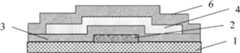
图1示出了在衬底上形成底栅电极后的结构图;Figure 1 shows a structural diagram after forming a bottom gate electrode on a substrate;
图2示出了在形成底栅介质层、有源区和有源区保护层后的结构示意图;Fig. 2 shows the structural diagram after forming the bottom gate dielectric layer, active region and active region protection layer;
图3示出了形成顶栅介质层后的结构图;FIG. 3 shows a structural diagram after forming a top gate dielectric layer;
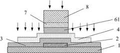
图4示了曝光时的结构示意图;Fig. 4 shows the schematic diagram of the structure during exposure;
图5示出了刻蚀形成顶栅介质和顶栅电极以及对源漏进行等离子处理的结构示意图;FIG. 5 shows a schematic structural diagram of etching to form a top gate dielectric and a top gate electrode and performing plasma treatment on the source and drain;
图6示出了图5去除光刻胶后的结构;Figure 6 shows the structure after removing the photoresist in Figure 5;
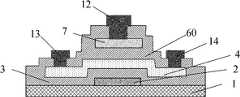
图7示出了形成晶体管各电极的接触孔的结构图;FIG. 7 shows a structural diagram of contact holes forming each electrode of the transistor;
图8示出了形成金属电极后的结构图。FIG. 8 shows a structure diagram after forming metal electrodes.
具体实施方式Detailed ways
下面通过具体实施方式结合附图对本发明作进一步详细说明。The present invention will be further described in detail below through specific embodiments in conjunction with the accompanying drawings.
现有技术中,双栅结构的薄膜晶体管其工艺方法决定了其顶栅电极和底栅电极不可能精确对准,这导致晶本管存在较大的寄生电容,使其性能受到限制。本发明在制作底栅电极时,采用不透光的设计,例如可采用不透光的材料,在制作衬底、顶栅电极以及底栅电极和顶栅电极之间的各层时采用具有透光特性的设计,例如可采用透光材料或通过厚度的设计使其具有透光特性;在光刻形成顶栅电极图案时,通过从衬底的背面向上曝光,使底栅电极起到天然掩模版的作用,提高了最终形成的顶栅电极和底栅电极的对准精度。具体地,本发明形成双栅结构的薄膜晶体管的一种方法可以是:In the prior art, the process method of the thin film transistor with double gate structure determines that its top gate electrode and bottom gate electrode cannot be precisely aligned, which leads to a large parasitic capacitance of the crystal transistor and limits its performance. The present invention adopts an opaque design when making the bottom gate electrode. For example, an opaque material can be used. The design of light characteristics, such as the use of light-transmitting materials or the design of the thickness to make it have light-transmitting characteristics; when forming the top gate electrode pattern by photolithography, the bottom gate electrode can be used as a natural mask by exposing upward from the back of the substrate. The role of the template improves the alignment accuracy of the finally formed top gate electrode and bottom gate electrode. Specifically, a method for forming a thin film transistor with a double-gate structure in the present invention may be:
图1示出了在衬底上形成底栅电极后的结构图。衬底1采用玻璃或具有透光特性的衬底,用磁控溅射或热蒸的方法在衬底1上生长一层厚度为100~300nm的不透明薄膜,该薄膜的材料可以是铬、钼、钛或铝等;通过光刻或刻蚀该薄膜形成底栅电极2。FIG. 1 shows a structure diagram after forming a bottom gate electrode on a substrate. The
图2示出了在形成底栅介质层、有源区和有源区保护层后的结构示意图。首先,在衬底1和底部栅电极2上生长一层绝缘介质薄膜,使其覆盖底部栅电极2并延伸到衬底1上,例如可以采用等离子增强化学汽相淀积PECVD的方法生长一层100~400nm厚的绝缘介质薄膜,该绝缘介质薄膜可以是氮化硅薄膜或氧化硅薄膜,该绝缘介质薄膜作为底栅介质层3,也可以采用磁控溅射法生长一层100~400nm厚的金属氧化物薄膜,其材料可以是氧化铝,氧化钽或氧化铪等;然后,底栅介质层3上依次淀积一层50~200nm厚的非晶或多晶的金属氧化物薄膜和20~80nm厚的金属氧化物薄膜或绝缘介质薄膜,可以采用射频磁控溅射的方法实现,经光刻和刻蚀分别形成有源区4和有源区保护层5。用于形成有源区的非晶或多晶的金属氧化物薄膜的材料可以是氧化锌基或氧化铟等,当为氧化铟时,溅射生长所述氧化铟金属氧化物半导体薄膜所述的陶瓷靶的纯度等于或优于99.99%。FIG. 2 shows a schematic view of the structure after forming the bottom gate dielectric layer, the active region and the active region protection layer. First, a layer of insulating dielectric film is grown on the
图3示出了形成顶栅介质层后的结构图。在有源区保护层5的表面生长一层100~400nm厚的介质薄膜,该介质薄膜延伸并覆盖底栅介质层3,生长的方法可以是用磁控溅射的方法生长一层100~400nm厚的金属氧化物薄膜,其材料可以是氧化铝,氧化钽或氧化铪等;也可以是用磁控溅射的方法生长一层100~400nm厚的绝缘介质薄膜,其材料可以是氮化硅或氧化硅;也可以是等离子增强化学汽相淀积PECVD生长一层100~400nm厚的绝缘介质薄膜,其材料可以是氮化硅或氧化硅等。该金属氧化物薄膜或绝缘介质薄膜与有源区保护层5共同形成顶栅介质层6,有源区保护层5的材料可以与顶栅介质层3的材料相同,也可以不同。比如,一种实施方式中,图2中有源区保护层5采用氧化硅,图3绝缘介质薄膜的材料也为氧化硅。可以理解的是,如果在图2所示步骤中,只生长用于形成有源区的金属氧化物薄膜,经光刻和刻蚀形成有源区,没有同时形成有源区保护层5,则此步中,直接在有源区表面生长一层用于形成顶栅介质层6的金属氧化物薄膜或绝缘介质薄膜并延伸覆盖底栅介质层3的表面。在图2中形成有源区保护层5,可以通过有源区保护层5的阻挡作用保护有源区的上表面在后序的工艺过程中免受污染和损伤,尤其是在光刻和刻蚀形成有源区4和制造顶栅介质层6的过程中免受污染和损伤,主要污染和损伤来源于在光刻和刻蚀有源区4后,干法去胶或生长栅介质层6时使有源区表面出现缺陷,也有可能是基片在不同工序间传递时出现污染,导致器件的特性变坏。FIG. 3 shows a structure diagram after forming a top gate dielectric layer. A layer of 100-400nm thick dielectric film is grown on the surface of the
图4示出了曝光时的结构示意图。在图3结构的基础上,首先,采用射频磁控溅射淀积一层100~300nm厚的透明导电薄膜70,用于形成顶栅电极7的材料,该导电薄膜70的材料可以是氧化铟锡或氧化铝锌等。然后,在透明导电薄膜70的表面涂布一层正性光刻胶,曝光时,从衬底1的背面曝光,图示中箭头所示方向为曝光方向,然后进行显影。光刻显影后,形成的光刻胶图形为图示中的8,由于光刻中底部栅电极起到掩膜版的作用,因此光刻胶图形8的形状和大小与底部栅电极表面的形状和大小相同,并且两者之间正对。可以理解的是,涂布的光刻胶也可以负性的光刻胶,负性光刻胶经光刻显影后形成的图形与正性光刻胶形成的图形相反,此时要形成自对准的结构需采用剥离(lift-off)技术。Figure 4 shows a schematic diagram of the structure during exposure. On the basis of the structure in Fig. 3, firstly, a transparent conductive film 70 with a thickness of 100 to 300 nm is deposited by radio frequency magnetron sputtering, which is used to form the material of the
图5示出了刻蚀形成顶栅介质层和顶栅电极以及对源漏进行氩等离子处理的结构。刻蚀图4中覆盖有光刻胶图形8的顶栅介质6和导电薄膜70,分别形成顶栅介质层61和顶栅电极7。有源区4中,底栅电极2和顶栅电极7之间正对的区域是沟道区,沟道区两侧的区域分别为源区和漏区。在保留光刻胶8的情况下,对源区和漏区进行等离子处理,以减小源区和漏区自身的寄生电阻。图示中,箭头所示方向为等离子的轰击方向,处理时,采用氩、氢或氨等气体轰击源区和漏区的表面,增加其载流子浓度,从而减小其寄生电阻的值。比如,一种实施方式中,采用的氩等离子的能量为100~200W,气压为0.1~1Torr。同时,轰击时,由于光刻胶图形8对顶栅电极7有保护作用,不必担心等离子处理对顶栅电极造成影响。FIG. 5 shows a structure in which a top gate dielectric layer and a top gate electrode are formed by etching and argon plasma treatment is performed on the source and drain. The
图6示出了图5去除光刻胶后的结构。去除顶栅电极7上的光刻胶8,可以采用丙酮超声的方法或干法去胶去除。FIG. 6 shows the structure of FIG. 5 after removing the photoresist. The
图7示出了形成晶体管各电极的接触孔的结构图。在图6结构的基础上,用磁控溅射法或等离子增强化学汽相淀积PECVD淀积一层100~300nm厚的氮化硅层60,然后光刻和刻蚀形成各电极的引出接触孔。在一种实施方式中,9为栅极接触孔,10为源极接触孔,11为漏极接触孔。FIG. 7 shows a structural diagram of contact holes forming respective electrodes of a transistor. On the basis of the structure in Fig. 6, a
图8示出了形成金属电极后的结构图。在图7结构的基础上用磁控溅射法淀积一层100~300nm厚的金属钛膜,然后光刻和刻蚀形成晶体管各电极的金属引出电极和互连线,同时连接顶部栅电极7和底部栅电极2。在一种实施方式中,12为栅极引出线,13为源极引出线,14为漏极引出线。FIG. 8 shows a structure diagram after forming metal electrodes. On the basis of the structure in Figure 7, deposit a layer of 100-300nm thick metal titanium film by magnetron sputtering, then photolithography and etching form the metal lead-out electrodes and interconnection lines of each electrode of the transistor, and connect the top gate electrode at the
采用以上方法制作的双栅金属氧化物薄膜晶体管,由于底栅电极和顶栅电极之间正对准,使得寄生电容等寄生元件的值减小或没有,从而提高了晶体管的性能。For the dual-gate metal oxide thin film transistor manufactured by the above method, due to the positive alignment between the bottom gate electrode and the top gate electrode, the value of parasitic elements such as parasitic capacitance is reduced or eliminated, thereby improving the performance of the transistor.
以上内容是结合具体的实施方式对本发明所作的进一步详细说明,不能认定本发明的具体实施只局限于这些说明。对于本发明所属技术领域的普通技术人员来说,在不脱离本发明构思的前提下,还可以做出若干简单推演或替换,都应当视为属于本发明的保护范围。The above content is a further detailed description of the present invention in conjunction with specific embodiments, and it cannot be assumed that the specific implementation of the present invention is limited to these descriptions. For those of ordinary skill in the technical field of the present invention, without departing from the concept of the present invention, some simple deduction or replacement can be made, which should be regarded as belonging to the protection scope of the present invention.
Claims (10)
Translated fromChinesePriority Applications (3)
| Application Number | Priority Date | Filing Date | Title |
|---|---|---|---|
| CN2010105683035ACN102130009B (en) | 2010-12-01 | 2010-12-01 | Manufacturing method of transistor |
| US13/376,834US9129992B2 (en) | 2010-12-01 | 2011-06-13 | Method for manufacturing transistor |
| PCT/CN2011/075635WO2012071878A1 (en) | 2010-12-01 | 2011-06-13 | Manufacturing method of a transistor |
Applications Claiming Priority (1)
| Application Number | Priority Date | Filing Date | Title |
|---|---|---|---|
| CN2010105683035ACN102130009B (en) | 2010-12-01 | 2010-12-01 | Manufacturing method of transistor |
Publications (2)
| Publication Number | Publication Date |
|---|---|
| CN102130009Atrue CN102130009A (en) | 2011-07-20 |
| CN102130009B CN102130009B (en) | 2012-12-05 |
Family
ID=44268037
Family Applications (1)
| Application Number | Title | Priority Date | Filing Date |
|---|---|---|---|
| CN2010105683035AActiveCN102130009B (en) | 2010-12-01 | 2010-12-01 | Manufacturing method of transistor |
Country Status (3)
| Country | Link |
|---|---|
| US (1) | US9129992B2 (en) |
| CN (1) | CN102130009B (en) |
| WO (1) | WO2012071878A1 (en) |
Cited By (23)
| Publication number | Priority date | Publication date | Assignee | Title |
|---|---|---|---|---|
| CN102593008A (en)* | 2012-02-29 | 2012-07-18 | 北京大学 | Method for preparing bottom gate self alignment zino oxide film transistor |
| CN103094205A (en)* | 2013-02-04 | 2013-05-08 | 广州新视界光电科技有限公司 | Prepared method of thin film transistor and thin film transistor driving back panel and thin film transistor driving back panel |
| CN103187302A (en)* | 2012-01-03 | 2013-07-03 | 财团法人工业技术研究院 | Method for operating transistor |
| CN103296090A (en)* | 2012-12-28 | 2013-09-11 | 昆山工研院新型平板显示技术中心有限公司 | Metallic oxide thin film transistor and manufacturing method thereof |
| CN103456744A (en)* | 2013-09-05 | 2013-12-18 | 北京京东方光电科技有限公司 | Array substrate, preparing method of array substrate and display device |
| WO2014085971A1 (en)* | 2012-12-04 | 2014-06-12 | 深圳市柔宇科技有限公司 | Metallic oxide tft device and manufacturing method |
| CN103887345A (en)* | 2014-03-28 | 2014-06-25 | 南京中电熊猫液晶显示科技有限公司 | Oxide thin-film transistor and manufacturing method thereof |
| CN103988307A (en)* | 2011-08-02 | 2014-08-13 | 希百特股份有限公司 | Self-aligned metal oxide TFT with reduced number of masks |
| CN104576747A (en)* | 2013-10-18 | 2015-04-29 | 三星显示有限公司 | Thin film transistor, display panel having the same and method of manufacturing the same |
| CN105742240A (en)* | 2016-04-05 | 2016-07-06 | 武汉华星光电技术有限公司 | Fabrication method of low temperature poly-silicon (LTPS) array substrate |
| CN105914158A (en)* | 2016-05-10 | 2016-08-31 | 中国科学院微电子研究所 | Preparation method of metal graphene double-sided contact structure and graphene transistor |
| CN106098784A (en)* | 2016-06-13 | 2016-11-09 | 武汉华星光电技术有限公司 | Coplanar type double grid electrode oxide thin film transistor and preparation method thereof |
| WO2017124690A1 (en)* | 2016-01-19 | 2017-07-27 | 深圳市华星光电技术有限公司 | Manufacturing method for thin-film transistor structure |
| CN107946195A (en)* | 2017-04-27 | 2018-04-20 | 北京大学深圳研究生院 | The method for preparing dual gate oxide semiconductor thin-film transistor |
| CN108172624A (en)* | 2016-12-07 | 2018-06-15 | 清华大学 | A kind of thin film transistor and its preparation method |
| CN108172627A (en)* | 2016-12-07 | 2018-06-15 | 清华大学 | A kind of thin film transistor and its preparation method |
| CN108172628A (en)* | 2016-12-07 | 2018-06-15 | 清华大学 | a logic circuit |
| CN110942995A (en)* | 2019-11-26 | 2020-03-31 | 深圳市华星光电半导体显示技术有限公司 | Top gate type oxide array substrate and preparation method thereof |
| CN111201590A (en)* | 2017-12-07 | 2020-05-26 | 深圳市柔宇科技有限公司 | Thin film transistor, preparation method thereof, array substrate and display device |
| CN111477742A (en)* | 2019-01-24 | 2020-07-31 | 纽多维有限公司 | Organic thin film transistor and preparation method thereof |
| WO2020154983A1 (en)* | 2019-01-30 | 2020-08-06 | 深圳市柔宇科技有限公司 | Thin film transistor and fabrication method therefor, display panel and display device |
| CN112701045A (en)* | 2020-12-29 | 2021-04-23 | 北京大学深圳研究生院 | Structure and manufacturing method of double-gate thin film transistor |
| CN113380607A (en)* | 2021-05-11 | 2021-09-10 | 中国科学院微电子研究所 | Wafer exposure method |
Families Citing this family (35)
| Publication number | Priority date | Publication date | Assignee | Title |
|---|---|---|---|---|
| WO2011074407A1 (en) | 2009-12-18 | 2011-06-23 | Semiconductor Energy Laboratory Co., Ltd. | Semiconductor device and method for manufacturing the same |
| US9209314B2 (en) | 2010-06-16 | 2015-12-08 | Semiconductor Energy Laboratory Co., Ltd. | Field effect transistor |
| JP5975635B2 (en) | 2010-12-28 | 2016-08-23 | 株式会社半導体エネルギー研究所 | Semiconductor device |
| US9443984B2 (en) | 2010-12-28 | 2016-09-13 | Semiconductor Energy Laboratory Co., Ltd. | Semiconductor device and manufacturing method thereof |
| US9082663B2 (en) | 2011-09-16 | 2015-07-14 | Semiconductor Energy Laboratory Co., Ltd. | Semiconductor device and manufacturing method thereof |
| KR102504604B1 (en) | 2011-09-29 | 2023-02-27 | 가부시키가이샤 한도오따이 에네루기 켄큐쇼 | Semiconductor device |
| WO2013054933A1 (en) | 2011-10-14 | 2013-04-18 | Semiconductor Energy Laboratory Co., Ltd. | Semiconductor device |
| TWI613824B (en) | 2011-12-23 | 2018-02-01 | 半導體能源研究所股份有限公司 | Semiconductor device |
| US9379247B2 (en)* | 2012-06-28 | 2016-06-28 | Cbrite Inc. | High mobility stabile metal oxide TFT |
| US9269796B2 (en)* | 2013-02-06 | 2016-02-23 | Shenzhen Royole Technologies Co., Ltd. | Manufacturing method of a thin film transistor and pixel unit thereof |
| KR102446991B1 (en) | 2013-09-13 | 2022-09-26 | 가부시키가이샤 한도오따이 에네루기 켄큐쇼 | light emitting device |
| JP2016001712A (en) | 2013-11-29 | 2016-01-07 | 株式会社半導体エネルギー研究所 | Method for manufacturing semiconductor device |
| WO2015114476A1 (en) | 2014-01-28 | 2015-08-06 | Semiconductor Energy Laboratory Co., Ltd. | Semiconductor device |
| JP2015188062A (en) | 2014-02-07 | 2015-10-29 | 株式会社半導体エネルギー研究所 | semiconductor device |
| KR102295221B1 (en) | 2014-12-26 | 2021-09-01 | 삼성디스플레이 주식회사 | Gate driving circuit and display device having the same |
| CN104576760A (en)* | 2015-02-02 | 2015-04-29 | 合肥鑫晟光电科技有限公司 | Thin film transistor, manufacturing method thereof, array substrate and display device |
| CN104795496A (en)* | 2015-04-08 | 2015-07-22 | 深圳市华星光电技术有限公司 | Bigrid device and manufacturing method thereof |
| CN104867870B (en)* | 2015-04-14 | 2017-09-01 | 深圳市华星光电技术有限公司 | Manufacturing method and structure of double gate oxide semiconductor TFT substrate |
| CN104752343B (en)* | 2015-04-14 | 2017-07-28 | 深圳市华星光电技术有限公司 | The preparation method and its structure of dual gate oxide semiconductor TFT substrate |
| CN104900654B (en)* | 2015-04-14 | 2017-09-26 | 深圳市华星光电技术有限公司 | The preparation method and its structure of dual gate oxide semiconductor TFT substrate |
| CN104952880A (en)* | 2015-05-06 | 2015-09-30 | 深圳市华星光电技术有限公司 | Bi-grid TFT (thin film transistor) substrate manufacturing method and bi-grid TFT substrate structure |
| CN104900531A (en)* | 2015-06-08 | 2015-09-09 | 京东方科技集团股份有限公司 | Oxide thin-film transistor and array substrate, and manufacturing methods thereof, and display apparatus |
| TWI650817B (en)* | 2015-08-28 | 2019-02-11 | 聯華電子股份有限公司 | Semiconductor structure and method of forming the same |
| EP3236503A1 (en)* | 2016-04-18 | 2017-10-25 | IMEC vzw | Method for fabricating fully self-aligned dual-gate thin film transistors |
| US9881956B2 (en) | 2016-05-06 | 2018-01-30 | International Business Machines Corporation | Heterogeneous integration using wafer-to-wafer stacking with die size adjustment |
| CN106684155B (en)* | 2017-01-05 | 2021-03-30 | 京东方科技集团股份有限公司 | Double-gate thin film transistor and preparation method thereof, array substrate and display device |
| US10446681B2 (en)* | 2017-07-10 | 2019-10-15 | Micron Technology, Inc. | NAND memory arrays, and devices comprising semiconductor channel material and nitrogen |
| US11658222B2 (en)* | 2017-09-27 | 2023-05-23 | Intel Corporation | Thin film transistor with charge trap layer |
| US10297611B1 (en) | 2017-12-27 | 2019-05-21 | Micron Technology, Inc. | Transistors and arrays of elevationally-extending strings of memory cells |
| US10559466B2 (en) | 2017-12-27 | 2020-02-11 | Micron Technology, Inc. | Methods of forming a channel region of a transistor and methods used in forming a memory array |
| GB2610886B (en) | 2019-08-21 | 2023-09-13 | Pragmatic Printing Ltd | Resistor geometry |
| GB2587793B (en)* | 2019-08-21 | 2023-03-22 | Pragmatic Printing Ltd | Electronic circuit comprising transistor and resistor |
| CN111081873A (en)* | 2019-11-18 | 2020-04-28 | 天津大学 | A kind of high-transparency flexible thin-film transistor and manufacturing method |
| US11538919B2 (en) | 2021-02-23 | 2022-12-27 | Micron Technology, Inc. | Transistors and arrays of elevationally-extending strings of memory cells |
| CN113809163B (en)* | 2021-09-17 | 2023-11-24 | 武汉天马微电子有限公司 | Metal oxide transistor, display panel and display device |
Citations (7)
| Publication number | Priority date | Publication date | Assignee | Title |
|---|---|---|---|---|
| JPS6146067A (en)* | 1984-08-10 | 1986-03-06 | Nec Corp | Double gate thin film transistor and its manufacturing method |
| US20040183130A1 (en)* | 2003-03-20 | 2004-09-23 | Fujitsu Limited | Semiconductor device and method of fabricating the same |
| CN101013221A (en)* | 2007-01-16 | 2007-08-08 | 友达光电股份有限公司 | Manufacturing method of color filter layer |
| CN101442104A (en)* | 2007-11-21 | 2009-05-27 | 中国科学院微电子研究所 | A Method of Simultaneously Defining the Source, Drain and Gate Electrodes of Organic Thin Film Transistors by One Mask Lithography |
| CN101488459A (en)* | 2009-02-13 | 2009-07-22 | 北京大学深圳研究生院 | Production method for self-aligned metallic oxide thin-film transistor |
| CN101533779A (en)* | 2009-04-03 | 2009-09-16 | 北京大学深圳研究生院 | Manufacturing method for film transistor and image display device |
| CN101542744A (en)* | 2007-07-02 | 2009-09-23 | 韩国机械研究院 | Self-aligned organic thin film transistor and fabrication method thereof |
Family Cites Families (7)
| Publication number | Priority date | Publication date | Assignee | Title |
|---|---|---|---|---|
| GB9919913D0 (en)* | 1999-08-24 | 1999-10-27 | Koninkl Philips Electronics Nv | Thin-film transistors and method for producing the same |
| US6673661B1 (en)* | 2002-12-20 | 2004-01-06 | Taiwan Semiconductor Manufacturing Co., Ltd. | Self-aligned method for forming dual gate thin film transistor (TFT) device |
| KR100585873B1 (en)* | 2003-11-03 | 2006-06-07 | 엘지.필립스 엘시디 주식회사 | Polysilicon Liquid Crystal Display Device and Manufacturing Method Thereof |
| GB0401579D0 (en)* | 2004-01-24 | 2004-02-25 | Koninkl Philips Electronics Nv | Transistor manufacture |
| WO2007142167A1 (en)* | 2006-06-02 | 2007-12-13 | Kochi Industrial Promotion Center | Semiconductor device including an oxide semiconductor thin film layer of zinc oxide and manufacturing method thereof |
| KR101345378B1 (en)* | 2007-05-17 | 2013-12-24 | 삼성전자주식회사 | Fabrication method of ZnO family Thin film transistor |
| KR101496148B1 (en)* | 2008-05-15 | 2015-02-27 | 삼성전자주식회사 | Semiconductor device and manufacturing method thereof |
- 2010
- 2010-12-01CNCN2010105683035Apatent/CN102130009B/enactiveActive
- 2011
- 2011-06-13USUS13/376,834patent/US9129992B2/enactiveActive
- 2011-06-13WOPCT/CN2011/075635patent/WO2012071878A1/enactiveApplication Filing
Patent Citations (7)
| Publication number | Priority date | Publication date | Assignee | Title |
|---|---|---|---|---|
| JPS6146067A (en)* | 1984-08-10 | 1986-03-06 | Nec Corp | Double gate thin film transistor and its manufacturing method |
| US20040183130A1 (en)* | 2003-03-20 | 2004-09-23 | Fujitsu Limited | Semiconductor device and method of fabricating the same |
| CN101013221A (en)* | 2007-01-16 | 2007-08-08 | 友达光电股份有限公司 | Manufacturing method of color filter layer |
| CN101542744A (en)* | 2007-07-02 | 2009-09-23 | 韩国机械研究院 | Self-aligned organic thin film transistor and fabrication method thereof |
| CN101442104A (en)* | 2007-11-21 | 2009-05-27 | 中国科学院微电子研究所 | A Method of Simultaneously Defining the Source, Drain and Gate Electrodes of Organic Thin Film Transistors by One Mask Lithography |
| CN101488459A (en)* | 2009-02-13 | 2009-07-22 | 北京大学深圳研究生院 | Production method for self-aligned metallic oxide thin-film transistor |
| CN101533779A (en)* | 2009-04-03 | 2009-09-16 | 北京大学深圳研究生院 | Manufacturing method for film transistor and image display device |
Cited By (36)
| Publication number | Priority date | Publication date | Assignee | Title |
|---|---|---|---|---|
| CN103988307A (en)* | 2011-08-02 | 2014-08-13 | 希百特股份有限公司 | Self-aligned metal oxide TFT with reduced number of masks |
| CN103988307B (en)* | 2011-08-02 | 2017-03-08 | 希百特股份有限公司 | The autoregistration metal-oxide TFT that mask count reduces |
| CN103187302A (en)* | 2012-01-03 | 2013-07-03 | 财团法人工业技术研究院 | Method for operating transistor |
| CN102593008A (en)* | 2012-02-29 | 2012-07-18 | 北京大学 | Method for preparing bottom gate self alignment zino oxide film transistor |
| CN102593008B (en)* | 2012-02-29 | 2015-10-21 | 京东方科技集团股份有限公司 | A kind of preparation method of bottom gate self alignment zino oxide film transistor |
| US9543328B2 (en) | 2012-12-04 | 2017-01-10 | Shenzhen Royole Technologies Co., Ltd. | Metal oxide TFT device and method for manufacturing the same |
| WO2014085971A1 (en)* | 2012-12-04 | 2014-06-12 | 深圳市柔宇科技有限公司 | Metallic oxide tft device and manufacturing method |
| CN103296090A (en)* | 2012-12-28 | 2013-09-11 | 昆山工研院新型平板显示技术中心有限公司 | Metallic oxide thin film transistor and manufacturing method thereof |
| CN103296090B (en)* | 2012-12-28 | 2016-02-03 | 昆山工研院新型平板显示技术中心有限公司 | A kind of metal oxide thin-film transistor and preparation method thereof |
| CN103094205B (en)* | 2013-02-04 | 2015-11-18 | 广州新视界光电科技有限公司 | A kind of thin-film transistor, thin-film transistor drive the preparation method of backboard and thin-film transistor to drive backboard |
| CN103094205A (en)* | 2013-02-04 | 2013-05-08 | 广州新视界光电科技有限公司 | Prepared method of thin film transistor and thin film transistor driving back panel and thin film transistor driving back panel |
| CN103456744A (en)* | 2013-09-05 | 2013-12-18 | 北京京东方光电科技有限公司 | Array substrate, preparing method of array substrate and display device |
| CN103456744B (en)* | 2013-09-05 | 2016-08-17 | 北京京东方光电科技有限公司 | Array base palte and preparation method thereof, display device |
| CN104576747A (en)* | 2013-10-18 | 2015-04-29 | 三星显示有限公司 | Thin film transistor, display panel having the same and method of manufacturing the same |
| CN103887345A (en)* | 2014-03-28 | 2014-06-25 | 南京中电熊猫液晶显示科技有限公司 | Oxide thin-film transistor and manufacturing method thereof |
| WO2017124690A1 (en)* | 2016-01-19 | 2017-07-27 | 深圳市华星光电技术有限公司 | Manufacturing method for thin-film transistor structure |
| CN105742240A (en)* | 2016-04-05 | 2016-07-06 | 武汉华星光电技术有限公司 | Fabrication method of low temperature poly-silicon (LTPS) array substrate |
| CN105742240B (en)* | 2016-04-05 | 2019-09-13 | 武汉华星光电技术有限公司 | A kind of manufacturing method of LTPS array substrate |
| US10157940B2 (en) | 2016-04-05 | 2018-12-18 | Wuhan China Star Optoelectronics Technology Co., Ltd. | Method for manufacturing LTPS array substrate |
| CN105914158B (en)* | 2016-05-10 | 2018-09-11 | 中国科学院微电子研究所 | Preparation method of metal graphene double-sided contact structure and graphene transistor |
| CN105914158A (en)* | 2016-05-10 | 2016-08-31 | 中国科学院微电子研究所 | Preparation method of metal graphene double-sided contact structure and graphene transistor |
| WO2017215138A1 (en)* | 2016-06-13 | 2017-12-21 | 武汉华星光电技术有限公司 | Coplanar double-gate electrode oxide thin-film transistor and preparation method therefor |
| CN106098784A (en)* | 2016-06-13 | 2016-11-09 | 武汉华星光电技术有限公司 | Coplanar type double grid electrode oxide thin film transistor and preparation method thereof |
| US10205027B2 (en) | 2016-06-13 | 2019-02-12 | Wuhan China Star Optoelectronics Technology Co., Ltd | Coplanar double gate electrode oxide thin film transistor and manufacture method thereof |
| CN108172624A (en)* | 2016-12-07 | 2018-06-15 | 清华大学 | A kind of thin film transistor and its preparation method |
| CN108172628A (en)* | 2016-12-07 | 2018-06-15 | 清华大学 | a logic circuit |
| CN108172627A (en)* | 2016-12-07 | 2018-06-15 | 清华大学 | A kind of thin film transistor and its preparation method |
| CN108172628B (en)* | 2016-12-07 | 2020-11-06 | 清华大学 | Logic circuit |
| CN108172627B (en)* | 2016-12-07 | 2020-11-06 | 清华大学 | A kind of thin film transistor and preparation method thereof |
| CN107946195A (en)* | 2017-04-27 | 2018-04-20 | 北京大学深圳研究生院 | The method for preparing dual gate oxide semiconductor thin-film transistor |
| CN111201590A (en)* | 2017-12-07 | 2020-05-26 | 深圳市柔宇科技有限公司 | Thin film transistor, preparation method thereof, array substrate and display device |
| CN111477742A (en)* | 2019-01-24 | 2020-07-31 | 纽多维有限公司 | Organic thin film transistor and preparation method thereof |
| WO2020154983A1 (en)* | 2019-01-30 | 2020-08-06 | 深圳市柔宇科技有限公司 | Thin film transistor and fabrication method therefor, display panel and display device |
| CN110942995A (en)* | 2019-11-26 | 2020-03-31 | 深圳市华星光电半导体显示技术有限公司 | Top gate type oxide array substrate and preparation method thereof |
| CN112701045A (en)* | 2020-12-29 | 2021-04-23 | 北京大学深圳研究生院 | Structure and manufacturing method of double-gate thin film transistor |
| CN113380607A (en)* | 2021-05-11 | 2021-09-10 | 中国科学院微电子研究所 | Wafer exposure method |
Also Published As
| Publication number | Publication date |
|---|---|
| US20130309808A1 (en) | 2013-11-21 |
| US9129992B2 (en) | 2015-09-08 |
| WO2012071878A1 (en) | 2012-06-07 |
| CN102130009B (en) | 2012-12-05 |
Similar Documents
| Publication | Publication Date | Title |
|---|---|---|
| CN102130009A (en) | A method of manufacturing a transistor | |
| US7635616B2 (en) | TFT LCD array substrate and manufacturing method thereof | |
| CN106684037B (en) | Optimize the tft array preparation method of 4M processing procedure | |
| CN101488459B (en) | A method of fabricating a self-aligned metal oxide thin film transistor | |
| US10707236B2 (en) | Array substrate, manufacturing method therefor and display device | |
| CN101630640B (en) | Photoresist burr edge-forming method and TFT-LCD array substrate-manufacturing method | |
| CN104752343B (en) | The preparation method and its structure of dual gate oxide semiconductor TFT substrate | |
| CN103021939B (en) | Array substrate, manufacture method of array substrate and display device | |
| WO2014012334A1 (en) | Manufacturing method of array substrate and array substrate and display device | |
| CN104867870B (en) | Manufacturing method and structure of double gate oxide semiconductor TFT substrate | |
| CN107994066B (en) | TFT, manufacturing method, array substrate, display panel and device | |
| CN103227147B (en) | TFT-LCD array substrate and manufacture method, liquid crystal display | |
| CN107871753B (en) | Array substrate and preparation method thereof | |
| CN102023433A (en) | TFT-LCD array substrate and method for manufacturing the same | |
| WO2016201609A1 (en) | Metal oxide thin-film transistor and display panel, and preparation methods for both | |
| CN104617152A (en) | Oxide film transistor and manufacturing method thereof | |
| WO2013181909A1 (en) | Thin-film transistor and array substrate and methods of fabricating same | |
| CN102593183A (en) | Thin film transistor structure and manufacturing method thereof | |
| CN103489921A (en) | Thin film transistor, manufacturing method thereof, array substrate and display device | |
| US9966450B2 (en) | Dual-gate TFT array substrate and manufacturing method thereof | |
| CN103337462B (en) | Preparation method of thin film transistor | |
| US10529750B2 (en) | LTPS array substrate and method for producing the same | |
| CN102693938B (en) | Thin film transistor liquid crystal display, array substrate and manufacture method of array substrate | |
| WO2019127681A1 (en) | Array substrate and preparation method | |
| WO2016201610A1 (en) | Metal oxide thin-film transistor and preparation method therefor, and display panel and display device |
Legal Events
| Date | Code | Title | Description |
|---|---|---|---|
| C06 | Publication | ||
| PB01 | Publication | ||
| C10 | Entry into substantive examination | ||
| SE01 | Entry into force of request for substantive examination | ||
| C14 | Grant of patent or utility model | ||
| GR01 | Patent grant | ||
| ASS | Succession or assignment of patent right | Owner name:JINGDONGFANG SCIENCE AND TECHNOLOGY GROUP CO., LTD Free format text:FORMER OWNER: SHENZHEN GRADUATE SCHOOL OF PEKING UNIVERSITY Effective date:20131205 | |
| C41 | Transfer of patent application or patent right or utility model | ||
| COR | Change of bibliographic data | Free format text:CORRECT: ADDRESS; FROM: 518055 SHENZHEN, GUANGDONG PROVINCE TO: CHAOYANG, BEIJING | |
| TR01 | Transfer of patent right | Effective date of registration:20131205 Address after:No. 10 Jiuxianqiao Road, Beijing, Chaoyang District Patentee after:BOE Technology Group Co., Ltd. Address before:518055 Guangdong city in Shenzhen Province, Nanshan District City Xili Shenzhen University North Campus Patentee before:Shenzhen Graduate School of Peking University |