CN102122217B - Optical touch display device - Google Patents
Optical touch display deviceDownload PDFInfo
- Publication number
- CN102122217B CN102122217BCN2010100032343ACN201010003234ACN102122217BCN 102122217 BCN102122217 BCN 102122217BCN 2010100032343 ACN2010100032343 ACN 2010100032343ACN 201010003234 ACN201010003234 ACN 201010003234ACN 102122217 BCN102122217 BCN 102122217B
- Authority
- CN
- China
- Prior art keywords
- light
- display device
- display panel
- optical touch
- touch display
- Prior art date
- Legal status (The legal status is an assumption and is not a legal conclusion. Google has not performed a legal analysis and makes no representation as to the accuracy of the status listed.)
- Expired - Fee Related
Links
- 230000003287optical effectEffects0.000titleclaimsabstractdescription80
- 238000000926separation methodMethods0.000claimsabstractdescription12
- 230000005540biological transmissionEffects0.000claimsabstractdescription10
- 239000000758substrateSubstances0.000claimsdescription15
- 239000012788optical filmSubstances0.000claimsdescription11
- 239000004973liquid crystal related substanceSubstances0.000claimsdescription7
- 239000010408filmSubstances0.000claimsdescription6
- 238000009792diffusion processMethods0.000claimsdescription5
- 230000000295complement effectEffects0.000claimsdescription2
- 229910044991metal oxideInorganic materials0.000claimsdescription2
- 150000004706metal oxidesChemical class0.000claimsdescription2
- 239000004065semiconductorSubstances0.000claimsdescription2
- 238000000034methodMethods0.000description6
- 230000000694effectsEffects0.000description2
- 238000010586diagramMethods0.000description1
- 229910052736halogenInorganic materials0.000description1
- 150000002367halogensChemical class0.000description1
- 238000012986modificationMethods0.000description1
- 230000004048modificationEffects0.000description1
- 230000005693optoelectronicsEffects0.000description1
- 239000010409thin filmSubstances0.000description1
Images


Landscapes
- Position Input By Displaying (AREA)
Abstract
Description
Translated fromChinese【技术领域】【Technical field】
本发明是有关于一种触控显示装置,且特别是有关于一种光学触控显示装置。The present invention relates to a touch display device, and in particular to an optical touch display device.
【背景技术】【Background technique】
随着光电科技的进步,采用滑鼠来控制电脑及荧幕中的物件的方式已无法满足使用者的需求,因此,比滑鼠控制更为人性化的方法便逐渐被发展出来。在这些人性化的方法中,以手指触控的方式最接近于人类一般日常生活中的经验,特别是对于可能无法灵活地操作滑鼠的年长者或小孩,都能够轻易的采用手指来触控,这点可从一些自动提款机已采用触控荧幕来获得部分的证实。With the advancement of optoelectronic technology, the method of using a mouse to control objects in computers and screens can no longer meet the needs of users. Therefore, a more humanized method than mouse control has gradually been developed. Among these humanized methods, finger touch is the closest to human experience in daily life, especially for the elderly or children who may not be able to operate the mouse flexibly, they can easily use fingers to touch This is partly evidenced by the fact that some ATMs have adopted touch screens.
此外,传统的笔记本电脑若在不外接滑鼠的情况下,通常是借由位于按键旁的触控板及轨迹点(track point)来控制游标。然而,对一般使用者而言,利用按键旁的触控板或轨迹点来控制游标可能不如采用滑鼠灵活,而配置于荧幕上的触控装置可解决这样的问题。这是因为触控装置的控制方式是一种相当直觉化的控制方式,即使用者直接触碰荧幕来操作物件。如此一来,当触控装置应用于笔记本电脑中时,即使使用者是处于不方便外接滑鼠的操作环境下,仍能够利用触控装置来灵活流畅地操作。In addition, if a traditional notebook computer does not have an external mouse, the cursor is usually controlled by a touchpad and a track point located next to the buttons. However, for general users, using the touchpad or track point next to the button to control the cursor may not be as flexible as using a mouse, and the touch device configured on the screen can solve this problem. This is because the control method of the touch device is a rather intuitive control method, that is, the user directly touches the screen to operate the object. In this way, when the touch device is applied to a notebook computer, even if the user is in an operating environment where it is inconvenient to connect an external mouse, the touch device can still be used to operate flexibly and smoothly.
现今一般的触控装置的设计大致可区分为电阻式、电容式、光学式、声波式及电磁式等。以光学式触控显示装置而言,一般通常包含显示器、红外光源、导光单元、感测器及处理器,其中显示器包含背光模组与显示面板。红外光源设置于显示面旁用来产生红外光束,红外光源所产生的红外光束通过导光单元后被感测器所侦测。当触控物体接触面板时,处理器根据感测器所感测到的红外光强度变化来判断触碰点的位置。然而,由于红外光源与用以导引红外光的导光单元是设于显示面旁的前框上,这会导致显示面旁的结构过于凸出,进而造成显示器的外观不佳,而不具平面化的现代感。此外,红外光源与导光单元通常需要多组,这会导致光学元件数量增加及成本的增加,且会拉长组装的工时。Today's common touch devices can be roughly divided into resistive, capacitive, optical, acoustic, and electromagnetic designs. For an optical touch display device, it generally includes a display, an infrared light source, a light guide unit, a sensor, and a processor, wherein the display includes a backlight module and a display panel. The infrared light source is arranged beside the display surface to generate infrared light beams, and the infrared light beams generated by the infrared light source pass through the light guide unit and are detected by the sensor. When the touch object touches the panel, the processor judges the position of the touch point according to the change of the intensity of the infrared light sensed by the sensor. However, since the infrared light source and the light guide unit for guiding the infrared light are arranged on the front frame next to the display surface, this will cause the structure next to the display surface to protrude too much, which will cause the display to have a poor appearance and not have a flat surface. modernized. In addition, multiple sets of infrared light sources and light guide units are usually required, which will increase the number and cost of optical components, and prolong the man-hours of assembly.
【发明内容】【Content of invention】
本发明提供一种光学触控显示装置,至少具有较佳的外观、较低的成本及较易组装的其中一个优点。The present invention provides an optical touch display device, which has at least one of the advantages of better appearance, lower cost and easier assembly.
本发明的其他目的和优点可以从本发明所揭露的技术特征中得到进一步的了解。Other purposes and advantages of the present invention can be further understood from the technical features disclosed in the present invention.
为达上述之一或部份或全部目的或是其他目的,本发明之一实施例提出一种光学触控显示装置,包括至少一可见光发光元件、一光分布调整元件、一不可见光导光模组、至少一不可见光发光元件、一显示面板及至少一光侦测器。可见光发光元件适于发出一可见光束。光分布调整元件配置于可见光束的传递路径上。不可见光导光模组包括一导光单元及一分色单元。导光单元配置于来自光分布调整元件的可见光束的传递路径上,且具有一背对光分布调整元件的第一表面、一朝向光分布调整元件的第二表面及一连接第一表面与第二表面的侧面。分色单元配置于第二表面上。不可见光发光元件配置于侧面旁,且适于发出一不可见光束。不可见光束适于经由侧面进入导光单元。分色单元适于让可见光束通过,且适于将来自侧面的不可见光束反射至第一表面。显示面板配置于光分布调整元件的一侧,其中显示面板前有一感测空间,且显示面板位于光分布调整元件与感测空间之间。导光单元配置于光分布调整元件与感测空间之间,且不可见光束适于经由第一表面传递至感测空间。光侦测器配置于显示面板外。当一触控物体进入感测空间时,触控物体反射部分不可见光束,且光侦测器配置于被触控物体反射的部分不可见光束的传递路径上。In order to achieve one or part or all of the above objectives or other objectives, an embodiment of the present invention proposes an optical touch display device, including at least one visible light emitting element, a light distribution adjusting element, an invisible light guiding light module A group, at least one invisible light emitting element, a display panel and at least one light detector. The visible light emitting element is suitable for emitting a visible light beam. The light distribution adjustment element is arranged on the transmission path of the visible light beam. The invisible light guide module includes a light guide unit and a color separation unit. The light guide unit is arranged on the transmission path of the visible light beam from the light distribution adjustment element, and has a first surface facing away from the light distribution adjustment element, a second surface facing the light distribution adjustment element, and a connection between the first surface and the second surface. The side of the second surface. The color separation unit is configured on the second surface. The invisible light emitting element is arranged beside the side and is suitable for emitting an invisible light beam. The invisible light beam is adapted to enter the light guide unit via the side. The dichroic unit is suitable for passing the visible light beam and reflecting the invisible light beam from the side to the first surface. The display panel is arranged on one side of the light distribution adjustment element, wherein there is a sensing space in front of the display panel, and the display panel is located between the light distribution adjustment element and the sensing space. The light guide unit is disposed between the light distribution adjusting element and the sensing space, and the invisible light beam is adapted to be transmitted to the sensing space through the first surface. The light detector is arranged outside the display panel. When a touch object enters the sensing space, the touch object reflects part of the invisible light beam, and the light detector is arranged on the transmission path of the part of the invisible light beam reflected by the touch object.
基于上述,本发明的实施例至少具有以下其中一个优点,由于本发明之实施例之光学触控显示装置采用配置于光分布调整元件与感测空间之间的不可见光导光模组来提供不可见光源,因此光学触控显示装置的外观较为平整、较具美观。Based on the above, the embodiments of the present invention have at least one of the following advantages, because the optical touch display device of the embodiments of the present invention adopts an invisible light guide module arranged between the light distribution adjustment element and the sensing space to provide invisible Visible light source, so the appearance of the optical touch display device is relatively smooth and beautiful.
为让本发明之上述特征和优点能更明显易懂,下文特举实施例,并配合所附图式作详细说明如下。In order to make the above-mentioned features and advantages of the present invention more comprehensible, the following specific embodiments are described in detail in conjunction with the accompanying drawings.
【附图说明】【Description of drawings】
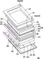
图1A为本发明之一实施例之光学触控显示装置的正视示意图。FIG. 1A is a schematic front view of an optical touch display device according to an embodiment of the present invention.
图1B为图1A之光学触控显示装置的爆炸图。FIG. 1B is an exploded view of the optical touch display device shown in FIG. 1A .
图1C为图1A之光学触控显示装置沿着I-I线的剖面示意图。FIG. 1C is a schematic cross-sectional view of the optical touch display device in FIG. 1A along line I-I.
图2为本发明之另一实施例之光学触控显示装置的剖面示意图。FIG. 2 is a schematic cross-sectional view of an optical touch display device according to another embodiment of the present invention.
图3为本发明之又一实施例之光学触控显示装置的正视示意图。FIG. 3 is a schematic front view of an optical touch display device according to another embodiment of the present invention.
图4为本发明之再一实施例之光学触控显示装置的剖面示意图。FIG. 4 is a schematic cross-sectional view of an optical touch display device according to yet another embodiment of the present invention.
50:触控物体50: Touch objects
100、100b、100c、100d:光学触控显示装置100, 100b, 100c, 100d: optical touch display device
110:显示面板110: display panel
112:主动元件阵列基板112: Active element array substrate
114:液晶层114: liquid crystal layer
116:对向基板116: opposite substrate
120、120a、120b、120c:光侦测器120, 120a, 120b, 120c: light detectors
130:处理单元130: processing unit
140:前框140: front frame
150、150b:背框150, 150b: back frame
210、210b:光分布调整元件210, 210b: light distribution adjusting element
212、214、216:表面212, 214, 216: surface
220:可见光发光元件220: Visible light emitting element
221:可见光束221: visible beam
240:反射单元240: reflection unit
250、250b、420:承载器250, 250b, 420: Carrier
260:光学膜片组260: Optical film set
300、300d:不可见光导光模组300, 300d: invisible light guide module
310、310d:导光单元310, 310d: light guide unit
311、313:散射微结构311, 313: Scattering microstructures
312:第一表面312: First Surface
314:第二表面314: second surface
316:侧面316: side
320、320d:分色单元320, 320d: color separation unit
410:不可见光发光元件410: Invisible light emitting element
412:不可见光束412: Invisible Beam
A:显示区A: display area
S:感测空间S: Sensing Space
【具体实施方式】【Detailed ways】
有关本发明的前述及其他技术内容、特点与功效,在以下配合参考图式之一较佳实施例的详细说明中,将可清楚的呈现。以下实施例中所提到的方向用语,例如:上、下、左、右、前或后等,仅是参考附加图式的方向。因此,使用的方向用语是用来说明并非用来限制本发明。The aforementioned and other technical contents, features and effects of the present invention will be clearly presented in the following detailed description of a preferred embodiment with reference to the drawings. The directional terms mentioned in the following embodiments, such as: up, down, left, right, front or back, etc., are only directions referring to the attached drawings. Accordingly, the directional terms are used to illustrate and not to limit the invention.
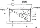
图1A为本发明之一实施例之光学触控显示装置的正视示意图,图1B为图1A之光学触控显示装置的爆炸图,且图1C为图1A之光学触控显示装置沿着I-I线的剖面示意图。请参照图1A至图1C,本实施例的光学触控显示装置100包括至少一可见光发光元件220(在本实施例中是以数个可见光发光元件220为例)、一光分布调整元件210、一不可见光导光模组300、至少一不可见光发光元件410(在本实施例中是以数个不可见光发光元件410为例)、一显示面板110及至少一光侦测器120(在本实施例中是以两个光侦测器120a与120b为例)。FIG. 1A is a schematic front view of an optical touch display device according to an embodiment of the present invention, FIG. 1B is an exploded view of the optical touch display device of FIG. 1A , and FIG. 1C is an I-I line of the optical touch display device of FIG. 1A sectional schematic diagram. 1A to 1C, the optical
可见光发光元件220适于发出一可见光束221(如图1C所绘示)。光分布调整元件210配置于可见光束221的传递路径上。在本实施例中,光分布调整元件210例如为一导光板,且具有一朝向显示面板110的表面212、一背对显示面板110的表面214及一连接表面212与表面214的入光面216。可见光发光元件220配置于入光面216旁,且可见光束221适于经由入光面216进入导光板210中,且适于经由表面214传递至显示面板110。可见光束221经过显示面板110的调制作用后,能够产生适于人眼观看的画面。在本实施例中,光学触控显示装置100更包括一反射单元240,配置于表面214上,以将来自入光面216的可见光束221反射至表面212。可见光发光元件220例如为可见光发光二极管(light emitting diode,LED),且可见光发光元件220可配置于一承载器250上。承载器250例如为一电路板,且可见光发光元件220电性连接至承载器250。The visible
不可见光导光模组300包括一导光单元310及一分色单元320。导光单元310配置于来自光分布调整元件210的可见光束221的传递路径上,且具有一背对光分布调整元件210的第一表面312、一朝向光分布调整元件210的第二表面314及一连接第一表面312与第二表面314的侧面316。在本实施例中,导光单元310例如为一导光板。分色单元320配置于第二表面314上。不可见光发光元件410配置于侧面316旁,且适于发出一不可见光束412。在本实施例中,不可见光发光元件410例如为一红外光发光二极管,且不可见光束412例如为一红外光束。不可见光束412适于经由侧面316进入导光单元310。在本实施例中,不可见光发光元件410可配置于一承载器420上,其中承载器420例如是一电性连接至这些不可见光发光元件410的电路板。分色单元320适于让可见光束221通过,且适于将来自侧面316的不可见光束412反射至第一表面312。在本实施例中,分色单元320例如为一适于让可见光通过且适于反射红外光的分色膜(dichroicfilm)。The invisible
显示面板110配置于光分布调整元件210的一侧,其中,显示面板110前有一感测空间S,且显示面板110位于光分布调整元件210与感测空间S之间。在本实施例中,不可见光导光模组300配置于光分布调整元件210与显示面板110之间。然而,在另一实施例中,不可见光导光模组300亦可以配置于显示面板110与感测空间S之间。在本实施例中,导光单元310配置于光分布调整元件210与感测空间S之间,且不可见光束412适于经由第一表面312传递至感测空间S。在本实施例中,不可见光导光模组300配置于光分布调整元件210与显示面板110之间。此外,导光单元310可具有数个散射微结构311,散射微结构311配置于第一表面312与第二表面314之至少其一上。散射微结构311例如为凹点、凸点、凹纹、凸纹或其组合。以图1C为例,散射微结构311例如为位于第一表面312上的凹点。在本实施例中,当不可见光束412经由侧面316进入导光单元310后,会不断地被第一表面312与第二表面314反射。散射微结构311可破坏此反射现象,而使不可见光束412因散射而离开导光单元310,并传递至显示面板110。接着,不可见光束412穿透显示面板110而传递至感测空间S。The
在本实施例中,显示面板110例如为一液晶显示面板,且显示面板110包括一主动元件阵列基板112、一液晶层114及一对向基板116。液晶层114配置于主动元件阵列基板112与对向基板116之间,且对向基板116配置于液晶层114与感测空间S之间。在本实施例中,主动元件阵列基板112例如为一薄膜电晶体阵列基板(thin film transistor array substrate,TFT array substrate),且对向基板116例如为一彩色滤光阵列基板。In this embodiment, the
光侦测器120配置于显示面板110外。在本实施例中,光侦测器120配置于感测空间S旁,且配置于显示面板110之背对光分布调整元件210的一侧。此外,在本实施例中,光侦测器120a与120b配置于显示面板110的显示区A之相邻两角落旁。光侦测器120例如为互补式金氧半导体感测元件(complementary metal oxide semiconductor sensor,CMOS sensor)、电荷耦合元件(charge coupled device,CCD)、光电倍增管(photomultiplier tube,PMT)或其他影像感测器。当一触控物体50(例如使用者的手指、触控笔的笔尖或其他适当的物体)进入感测空间S时,触控物体50反射部分不可见光束412,且光侦测器120配置于被触控物体50反射的部分不可见光束412的传递路径上。具体而言,当触控物体50进入感测空间S时,会使照射于触控物体50上的不可见光束412产生散射。如此一来,触控物体50会将部分不可见光束412反射至光侦测器120。此部分不可见光束412会在光侦测器120所侦测到的一画面上产生一亮区,其中此亮区例如为一亮点。The
此外,感测空间S中没有被触控物体50占据的其他部分由于没有物体可将不可见光束412反射至光侦测器120,因此会在光侦测器120所侦测到的画面上形成暗区(即暗背景)。光学触控显示装置100适于根据亮区在画面中的位置判断出触控物体50在感测空间S中的位置。具体而言,光学触控显示装置100可更包括一处理单元130,电性连接至光侦测器120,在本实施例中例如是同时电性连接至光侦测器120a与120b。处理单元130适于根据亮区在画面中的位置判断出触控物体50在感测空间S中的位置。In addition, other parts of the sensing space S that are not occupied by the
在本实施例中,光学触控显示装置100更包括一光学膜片组260,配置于光分布调整元件210与显示面板110之间,其中光学膜片组260包括增亮膜(brightness enhancement film,BEF)、棱镜片(prism sheet)及扩散片(diffusion sheet)之至少其一,亦即包括增亮膜、棱镜片、扩散片及其他光学膜片的任意组合。此外,在本实施例中,不可见光导光模组300配置于光学膜片组260与显示面板110之间。In this embodiment, the optical
在本实施例中,光学触控显示装置100更包括一前框140,覆盖显示面板110的边缘。光侦测器120配置于前框140上,且部分前框140位于光侦测器120与显示面板110的边缘之间。此外,在本实施例中,光侦测器120a与120b分别配置于前框140的相邻两角落上。再者,在本实施例中,光学触控显示装置100更包括一背框150,背框150用以容置承载器250及反射单元240。In this embodiment, the optical
本发明的实施例至少具有以下其中一个优点,由于本实施例之光学触控显示装置100采用配置于光分布调整元件210与感测空间S之间的不可见光导光模组300来提供不可见光源,因此本实施例之光学触控显示装置100的外观较为平整、较具美观。相较于习知光学触控显示装置的红外光源与用以导引红外光的导光单元是设于显示面旁的前框上,因而导致显示面旁的结构过于凸出,本实施例之光学触控显示装置100可避免如此之问题产生。再者,相较于习知光学触控显示装置的红外光源与导光单元通常需要多组,因而导致光学元件数量增加及成本的增加,且拉长组装的工时,本实施例可以将一个不可见光导光模组300结合至光学触控显示装置100中,因此光学结构较为简化,进而能够降低组装困难度、缩短组装工时及降低成本。The embodiment of the present invention has at least one of the following advantages, because the optical
值得注意的是,本发明并不限定可见光发光元件220必须是发光二极管,在其他实施例中,可见光发光元件220亦可以是荧光灯管、白炽灯泡、卤素灯泡或其他适当的发光元件。It is worth noting that the present invention does not limit the visible
图2为本发明之另一实施例之光学触控显示装置的剖面示意图。请参照图2,本实施例之光学触控显示装置100b与图1C之光学触控显示装置100类似,两者的差异如下所述。在本实施例之光学触控显示装置100b中,光分布调整元件210b为一扩散板。此外,光分布调整元件210b配置于每一可见光发光元件220与显示面板110之间,其中可见光束221适于穿透光分布调整元件210b而传递至显示面板110。在本实施例中,可见光发光元件220可在承载器250b上排列成二维阵列,且背框150b用以容置承载器250b及可见光发光元件220。本实施例之光学触控显示装置100b可达到与图1C之光学触控显示装置100类似的优点与功效,在此不再重述。FIG. 2 is a schematic cross-sectional view of an optical touch display device according to another embodiment of the present invention. Please refer to FIG. 2 , the optical
图3为本发明之又一实施例之光学触控显示装置的正视示意图。请参照图3,本实施例之光学触控显示装置100c与图1A之光学触控显示装置100类似,两者的差异如下所述。在本实施例中,光学触控显示装置100c具有三个光侦测器120,即光侦测器120a、120b、120c。在本实施例中,光侦测器120c配置于前框140的一边上,然而,在其他实施例中,光侦测器120c亦可以是配置于前框140的其他角落或其他边上。由于光学触控显示装置100具有三个光侦测器120,因此即使二个触控物体50同时进入感测空间S,处理单元130亦能准确判断出这二个触控物体50各自所处的位置,进而使光学触控显示装置100c达到准确的多点触控。FIG. 3 is a schematic front view of an optical touch display device according to another embodiment of the present invention. Please refer to FIG. 3 , the optical
值得注意的是,本发明并不限定光学触控显示装置100c所具有之光侦测器120的数量。当光侦测器120的数量越多时,光学触控显示装置能够达到更多点的触控。此外,当光侦测器120的数量只有一个时,可有效降低光学触控显示装置的成本,且在一实施例中,仅采用一个光侦测器120就足以感测触控物体50在一维空间上的位置变化,如此可应用于仅需简易触控功能的光学触控显示装置,例如提款机的荧幕。It should be noted that the present invention does not limit the number of
图4为本发明再一实施例之光学触控显示装置的剖面示意图。请参照图4,本实施例之光学触控显示装置100d与图1B之光学触控显示装置100类似,两者的差异在于光侦测器120的位置。在本实施例之光学触控显示装置100中,光侦测器120(例如光侦测器120a与光侦测器120b)配置于显示面板110之面向光分布调整元件210的一侧。在本实施例中,光侦测器120a与120b配置于不可见光导光模组300d之面向显示面板110的一侧。被触控物体50反射的部分不可见光束412穿透显示面板110而传递至光侦测器120a与120b。由于本实施例之光侦测器120配置于光学触控显示装置100d的内部,而不是配置于前框140上,因此可进一步美化光学触控显示装置100d的外观,且可减少光学触控显示装置100d的整体厚度。FIG. 4 is a schematic cross-sectional view of an optical touch display device according to yet another embodiment of the present invention. Please refer to FIG. 4 , the optical
此外,在本实施例中,不可见光导光模组300d配置于光分布调整元件210与光学膜片组260之间,但本发明并不以此为限。在其他实施例中,不可见光导光模组300d亦可以配置于光学膜片组260与显示面板110之间,或配置于显示面板110与感测空间S之间,或配置于显示面板110与部分前框140之间。In addition, in this embodiment, the invisible
再者,在本实施例中,分色单元320d例如为一分色镜(dichroicmirror)。此外,导光单元310d的第二表面314上可设有数个散射微结构313,且此散射微结构313例如为凸点。然而,在其他实施例中,散射微结构313亦可以是凹点、凸纹或凹纹。Furthermore, in this embodiment, the
综上所述,本发明之实施例可具有下列优点之至少其一。由于本发明之实施例之光学触控显示装置采用配置于光分布调整元件与感测空间之间的不可见光导光模组来提供不可见光源,因此光学触控显示装置的外观较为平整、较具美观。In summary, the embodiments of the present invention may have at least one of the following advantages. Since the optical touch display device of the embodiment of the present invention uses an invisible light guide module disposed between the light distribution adjustment element and the sensing space to provide an invisible light source, the appearance of the optical touch display device is relatively flat and relatively smooth. beautiful.
以上所述者,仅为本发明之较佳实施例而已,当不能以此限定本发明实施之范围,即大凡依本发明申请专利范围及发明说明内容所作之简单的等效变化与修饰,皆仍属本发明专利涵盖之范围内。另外本发明的任一实施例或申请专利范围不须达成本发明所揭露之全部目的或优点或特点。此外,摘要部分和标题仅是用来辅助专利文件搜寻之用,并非用来限制本发明之权利范围。The above are only preferred embodiments of the present invention, and should not limit the scope of the present invention, that is, all simple equivalent changes and modifications made according to the patent scope of the present invention and the description of the invention are all Still belong to the scope covered by the patent of the present invention. In addition, any embodiment or scope of claims of the present invention does not need to achieve all the objectives or advantages or features disclosed in the present invention. In addition, the abstract and the title are only used to assist the search of patent documents, and are not used to limit the scope of rights of the present invention.
Claims (19)
Translated fromChinesePriority Applications (1)
| Application Number | Priority Date | Filing Date | Title |
|---|---|---|---|
| CN2010100032343ACN102122217B (en) | 2010-01-11 | 2010-01-11 | Optical touch display device |
Applications Claiming Priority (1)
| Application Number | Priority Date | Filing Date | Title |
|---|---|---|---|
| CN2010100032343ACN102122217B (en) | 2010-01-11 | 2010-01-11 | Optical touch display device |
Publications (2)
| Publication Number | Publication Date |
|---|---|
| CN102122217A CN102122217A (en) | 2011-07-13 |
| CN102122217Btrue CN102122217B (en) | 2012-11-28 |
Family
ID=44250782
Family Applications (1)
| Application Number | Title | Priority Date | Filing Date |
|---|---|---|---|
| CN2010100032343AExpired - Fee RelatedCN102122217B (en) | 2010-01-11 | 2010-01-11 | Optical touch display device |
Country Status (1)
| Country | Link |
|---|---|
| CN (1) | CN102122217B (en) |
Families Citing this family (3)
| Publication number | Priority date | Publication date | Assignee | Title |
|---|---|---|---|---|
| TWI534685B (en)* | 2012-03-28 | 2016-05-21 | 友達光電股份有限公司 | Touch screen display device |
| TWI486844B (en)* | 2012-09-25 | 2015-06-01 | Au Optronics Corp | Optical touch device with scan ability |
| CN112383728B (en)* | 2020-11-03 | 2024-04-30 | 广州长嘉电子有限公司 | Single-key optical control borderless television and control method thereof |
Citations (2)
| Publication number | Priority date | Publication date | Assignee | Title |
|---|---|---|---|---|
| CN101477273A (en)* | 2007-12-31 | 2009-07-08 | 乐金显示有限公司 | Liquid crystal display to which infrared rays source is applied and multi-touch system using the same |
| CN101593785A (en)* | 2009-07-03 | 2009-12-02 | 友达光电股份有限公司 | Optical sensing element, manufacturing method thereof and optical touch device |
- 2010
- 2010-01-11CNCN2010100032343Apatent/CN102122217B/ennot_activeExpired - Fee Related
Patent Citations (2)
| Publication number | Priority date | Publication date | Assignee | Title |
|---|---|---|---|---|
| CN101477273A (en)* | 2007-12-31 | 2009-07-08 | 乐金显示有限公司 | Liquid crystal display to which infrared rays source is applied and multi-touch system using the same |
| CN101593785A (en)* | 2009-07-03 | 2009-12-02 | 友达光电股份有限公司 | Optical sensing element, manufacturing method thereof and optical touch device |
Also Published As
| Publication number | Publication date |
|---|---|
| CN102122217A (en) | 2011-07-13 |
Similar Documents
| Publication | Publication Date | Title |
|---|---|---|
| TWI492128B (en) | Optical touch display apparatus | |
| TWI522869B (en) | Optical touch display apparatus | |
| US9141235B2 (en) | Optical position detecting device and display device with position detecting function | |
| TW200523788A (en) | Coordinate detection system for a display monitor | |
| CN101582001A (en) | Touch screen, touch module and control method | |
| JP2012508913A (en) | Integrated touch sensing display device and manufacturing method thereof | |
| CN102053763B (en) | Optical position detection device and display device with position detection function | |
| CN102117151B (en) | Optical touch display device | |
| TW201409324A (en) | Touch display panel and optical touch panel thereof | |
| US20150035799A1 (en) | Optical touchscreen | |
| CN102662527B (en) | Touch Sensing Display Device | |
| US20210255668A1 (en) | Display Stack Topologies for Under-Display Optical Transceivers | |
| TWI410685B (en) | Light guide module, optical touch module, and method of increasing signal to noise ratio of optical touch module | |
| CN102096520B (en) | Optical touch device | |
| EP4285210A1 (en) | Electronic devices having moisture-insensitive optical touch sensors | |
| CN212160687U (en) | A biometric detection device | |
| US8773372B2 (en) | Optical plate structure for a touch panel, and touch display panel and touch liquid crystal display panel including the same | |
| CN102122217B (en) | Optical touch display device | |
| WO2021012702A1 (en) | Asymmetric brightness enhancement films for liquid crystal display assemblies | |
| CN102419660A (en) | Touch display device and operating method thereof | |
| TWI502417B (en) | Touch display apparatus and operation method thereof | |
| CN106293273B (en) | Touch base plate and touch control display apparatus | |
| CN103365487B (en) | Touch device and touch projection system | |
| CN102129330A (en) | Touch screen, touch module and control method | |
| CN101916151B (en) | Optical plate structure, touch display panel including same, and touch liquid crystal display |
Legal Events
| Date | Code | Title | Description |
|---|---|---|---|
| C06 | Publication | ||
| PB01 | Publication | ||
| C10 | Entry into substantive examination | ||
| SE01 | Entry into force of request for substantive examination | ||
| C14 | Grant of patent or utility model | ||
| GR01 | Patent grant | ||
| CF01 | Termination of patent right due to non-payment of annual fee | ||
| CF01 | Termination of patent right due to non-payment of annual fee | Granted publication date:20121128 Termination date:20200111 |