CN102110776A - High-performance Organic field effect transistor and preparation method thereof - Google Patents
High-performance Organic field effect transistor and preparation method thereofDownload PDFInfo
- Publication number
- CN102110776A CN102110776ACN2010105788982ACN201010578898ACN102110776ACN 102110776 ACN102110776 ACN 102110776ACN 2010105788982 ACN2010105788982 ACN 2010105788982ACN 201010578898 ACN201010578898 ACN 201010578898ACN 102110776 ACN102110776 ACN 102110776A
- Authority
- CN
- China
- Prior art keywords
- organic
- layer
- field effect
- effect transistor
- semiconductor layer
- Prior art date
- Legal status (The legal status is an assumption and is not a legal conclusion. Google has not performed a legal analysis and makes no representation as to the accuracy of the status listed.)
- Granted
Links
- 238000002360preparation methodMethods0.000titleabstractdescription21
- 238000002353field-effect transistor methodMethods0.000title1
- 230000005669field effectEffects0.000claimsabstractdescription47
- 239000004065semiconductorSubstances0.000claimsabstractdescription40
- 229920000642polymerPolymers0.000claimsabstractdescription33
- 229920001955polyphenylene etherPolymers0.000claimsabstractdescription31
- 239000004793PolystyreneSubstances0.000claimsabstractdescription28
- 229920002223polystyrenePolymers0.000claimsabstractdescription28
- 238000000034methodMethods0.000claimsabstractdescription22
- SLIUAWYAILUBJU-UHFFFAOYSA-NpentaceneChemical compoundC1=CC=CC2=CC3=CC4=CC5=CC=CC=C5C=C4C=C3C=C21SLIUAWYAILUBJU-UHFFFAOYSA-N0.000claimsabstractdescription20
- 239000000758substrateSubstances0.000claimsabstractdescription19
- 239000000203mixtureSubstances0.000claimsabstractdescription11
- 239000013078crystalSubstances0.000claimsabstractdescription8
- 239000000463materialSubstances0.000claimsdescription13
- CSCPPACGZOOCGX-UHFFFAOYSA-NAcetoneChemical compoundCC(C)=OCSCPPACGZOOCGX-UHFFFAOYSA-N0.000claimsdescription8
- LFQSCWFLJHTTHZ-UHFFFAOYSA-NEthanolChemical compoundCCOLFQSCWFLJHTTHZ-UHFFFAOYSA-N0.000claimsdescription8
- 238000000151depositionMethods0.000claimsdescription8
- IFLREYGFSNHWGE-UHFFFAOYSA-NtetraceneChemical compoundC1=CC=CC2=CC3=CC4=CC=CC=C4C=C3C=C21IFLREYGFSNHWGE-UHFFFAOYSA-N0.000claimsdescription7
- XBDYBAVJXHJMNQ-UHFFFAOYSA-NTetrahydroanthraceneNatural productsC1=CC=C2C=C(CCCC3)C3=CC2=C1XBDYBAVJXHJMNQ-UHFFFAOYSA-N0.000claimsdescription6
- 150000003384small moleculesChemical class0.000claimsdescription6
- 239000008367deionised waterSubstances0.000claimsdescription4
- 229910021641deionized waterInorganic materials0.000claimsdescription4
- 239000011259mixed solutionSubstances0.000claimsdescription4
- 239000010703siliconSubstances0.000claimsdescription4
- 229910052710siliconInorganic materials0.000claimsdescription4
- 238000001771vacuum depositionMethods0.000claimsdescription4
- XLYOFNOQVPJJNP-UHFFFAOYSA-NwaterChemical compoundOXLYOFNOQVPJJNP-UHFFFAOYSA-N0.000claimsdescription4
- 239000000919ceramicSubstances0.000claimsdescription2
- 238000001035dryingMethods0.000claimsdescription2
- 239000011521glassSubstances0.000claimsdescription2
- 125000005582pentacene groupChemical group0.000claimsdescription2
- 239000002861polymer materialSubstances0.000claimsdescription2
- 238000012986modificationMethods0.000abstractdescription15
- 230000004048modificationEffects0.000abstractdescription15
- 238000005457optimizationMethods0.000abstractdescription3
- 239000003989dielectric materialSubstances0.000abstractdescription2
- 238000004519manufacturing processMethods0.000abstract1
- 239000010410layerSubstances0.000description70
- 230000037230mobilityEffects0.000description20
- 239000010408filmSubstances0.000description7
- VYPSYNLAJGMNEJ-UHFFFAOYSA-NSilicium dioxideChemical compoundO=[Si]=OVYPSYNLAJGMNEJ-UHFFFAOYSA-N0.000description6
- 238000000089atomic force micrographMethods0.000description6
- HEDRZPFGACZZDS-UHFFFAOYSA-NChloroformChemical compoundClC(Cl)ClHEDRZPFGACZZDS-UHFFFAOYSA-N0.000description4
- 239000008186active pharmaceutical agentSubstances0.000description4
- 238000005227gel permeation chromatographyMethods0.000description4
- 239000000243solutionSubstances0.000description4
- 238000012360testing methodMethods0.000description4
- XUIMIQQOPSSXEZ-UHFFFAOYSA-NSiliconChemical compound[Si]XUIMIQQOPSSXEZ-UHFFFAOYSA-N0.000description3
- 230000008859changeEffects0.000description3
- PCHJSUWPFVWCPO-UHFFFAOYSA-NgoldChemical compound[Au]PCHJSUWPFVWCPO-UHFFFAOYSA-N0.000description3
- 229910052737goldInorganic materials0.000description3
- 239000010931goldSubstances0.000description3
- 229910052751metalInorganic materials0.000description3
- 239000002184metalSubstances0.000description3
- 238000011160researchMethods0.000description3
- 235000012239silicon dioxideNutrition0.000description3
- 239000000377silicon dioxideSubstances0.000description3
- 230000008021depositionEffects0.000description2
- 230000005684electric fieldEffects0.000description2
- 230000006872improvementEffects0.000description2
- 239000011810insulating materialSubstances0.000description2
- 238000002156mixingMethods0.000description2
- 238000000623plasma-assisted chemical vapour depositionMethods0.000description2
- 230000008569processEffects0.000description2
- 238000000746purificationMethods0.000description2
- 238000002207thermal evaporationMethods0.000description2
- 239000010409thin filmSubstances0.000description2
- RYGMFSIKBFXOCR-UHFFFAOYSA-NCopperChemical compound[Cu]RYGMFSIKBFXOCR-UHFFFAOYSA-N0.000description1
- 229910052581Si3N4Inorganic materials0.000description1
- BQCADISMDOOEFD-UHFFFAOYSA-NSilverChemical compound[Ag]BQCADISMDOOEFD-UHFFFAOYSA-N0.000description1
- 239000000956alloySubstances0.000description1
- 229910052782aluminiumInorganic materials0.000description1
- XAGFODPZIPBFFR-UHFFFAOYSA-NaluminiumChemical compound[Al]XAGFODPZIPBFFR-UHFFFAOYSA-N0.000description1
- 238000000137annealingMethods0.000description1
- 230000005540biological transmissionEffects0.000description1
- 230000015572biosynthetic processEffects0.000description1
- 239000003153chemical reaction reagentSubstances0.000description1
- 239000004020conductorSubstances0.000description1
- 238000007796conventional methodMethods0.000description1
- 229910052802copperInorganic materials0.000description1
- 239000010949copperSubstances0.000description1
- 238000013461designMethods0.000description1
- 238000005516engineering processMethods0.000description1
- 238000001704evaporationMethods0.000description1
- 230000008020evaporationEffects0.000description1
- 238000002474experimental methodMethods0.000description1
- 238000010438heat treatmentMethods0.000description1
- 239000012535impuritySubstances0.000description1
- AMGQUBHHOARCQH-UHFFFAOYSA-Nindium;oxotinChemical compound[In].[Sn]=OAMGQUBHHOARCQH-UHFFFAOYSA-N0.000description1
- 238000007641inkjet printingMethods0.000description1
- 239000012212insulatorSubstances0.000description1
- 238000002386leachingMethods0.000description1
- 238000012417linear regressionMethods0.000description1
- 238000001755magnetron sputter depositionMethods0.000description1
- 238000000691measurement methodMethods0.000description1
- 229910044991metal oxideInorganic materials0.000description1
- 150000004706metal oxidesChemical class0.000description1
- 150000002739metalsChemical class0.000description1
- 238000005232molecular self-assemblyMethods0.000description1
- SLYCYWCVSGPDFR-UHFFFAOYSA-NoctadecyltrimethoxysilaneChemical compoundCCCCCCCCCCCCCCCCCC[Si](OC)(OC)OCSLYCYWCVSGPDFR-UHFFFAOYSA-N0.000description1
- 239000012044organic layerSubstances0.000description1
- 230000003647oxidationEffects0.000description1
- 238000007254oxidation reactionMethods0.000description1
- 239000002245particleSubstances0.000description1
- -1polyphenylene EthylenePolymers0.000description1
- 239000012521purified sampleSubstances0.000description1
- HQVNEWCFYHHQES-UHFFFAOYSA-Nsilicon nitrideChemical compoundN12[Si]34N5[Si]62N3[Si]51N64HQVNEWCFYHHQES-UHFFFAOYSA-N0.000description1
- 229910052709silverInorganic materials0.000description1
- 239000004332silverSubstances0.000description1
- 238000003756stirringMethods0.000description1
- 238000003786synthesis reactionMethods0.000description1
- 238000012546transferMethods0.000description1
- 238000007738vacuum evaporationMethods0.000description1
Images


Landscapes
- Thin Film Transistor (AREA)
Abstract
Translated fromChineseDescription
Translated fromChinese技术领域technical field
本发明涉及一种高性能有机场效应晶体管及其制备方法。The invention relates to a high-performance organic field effect transistor and a preparation method thereof.
背景技术Background technique
自从上世纪80年代发明(Tsumura,A.;Koezuka,H.;Ando,T.Appl.Phys.Lett.1986,49,1210)有机场效应晶体管以来,有机场效应晶体管由于在柔性显示,有机集成电路等方面的潜在应用前景引起了人们的广泛研究兴趣。与无机晶体管相比,有机场效应晶体管具有制备工艺简单、成本低廉、重量轻、柔韧性好等优点。近几年来,有机场效应晶体管不论在新型稳定的有机半导体材料设计合成以及器件制备等各方面均取得了长足的发展。然而到目前为止,有机场效应晶体管的迁移率与无机器件相比差距仍然很大,严重制约了有机场效应晶体管的推广应用,因此器件迁移率的提高仍然是目前有机场效应晶体管研究的首要方向之一。Since the invention of organic field effect transistors (Tsumura, A.; Koezuka, H.; Ando, T.Appl.Phys.Lett.1986, 49, 1210) in the 1980s, organic field effect transistors have been organically integrated in flexible displays. The potential application prospects in circuits and other aspects have aroused people's extensive research interest. Compared with inorganic transistors, organic field effect transistors have the advantages of simple preparation process, low cost, light weight, and good flexibility. In recent years, organic field effect transistors have made great progress in design and synthesis of new stable organic semiconductor materials and device preparation. However, so far, the mobility of organic field effect transistors is still far behind that of inorganic devices, which seriously restricts the popularization and application of organic field effect transistors. Therefore, the improvement of device mobility is still the primary direction of research on organic field effect transistors. one.
目前研究发现,有机场效应晶体管的有机半导体层中接近介电层的前几分子层半导体的形貌对场效应晶体管的迁移率有着关键性影响。因此优化介电层和半导体层界面附近半导体分子堆积形貌对于提高器件迁移率至关重要。目前,世界上很多课题组都报道了基于介电层修饰的半导体形貌优化技术,其中使用自组装分子修饰介电层表面以优化介电层和半导体层界面性质的方法成果显著。鲍哲南等人最近报道了利用超平的十八烷基三甲氧基硅烷自组装晶膜修饰二氧化硅介电层,得到了迁移率高达3.0cm2/Vs的并五苯场效应晶体管(Y.Ito,A.Virkar,S.Mannsfeld,J.H.Oh,M.Toney,J.Locklin,Z.Bao,J.Am.Chem.Soc.2009,131,9396.)。另外,Schwartz的小组最近也利用自己合成的有机磷酸酯分子自组装层修饰介电层表面,得到了迁移率为2.5cm2/Vs的并五苯场效应晶体管(K.Liao,A.G.Ismail,L.Kreplak,J.Schwartz,I.G.Hill,Adv.Mater.2010,22,3081.)。尽管上述方法都能确实地提高场效应器件的迁移率,但是1)这些方法都是基于复杂的工艺流程,很难实现大规模大面积制备的需求;2)这些方法都基于不可屈挠的单分子自组装修饰层,无法应用于柔性有机半导体器件的制备。Current studies have found that the morphology of the first few molecular layers of semiconductors close to the dielectric layer in the organic semiconductor layer of an organic field effect transistor has a key influence on the mobility of the field effect transistor. Therefore, optimizing the stacking morphology of semiconductor molecules near the interface between the dielectric layer and the semiconductor layer is crucial to improving device mobility. At present, many research groups in the world have reported semiconductor morphology optimization technologies based on dielectric layer modification, among which the method of using self-assembled molecules to modify the surface of the dielectric layer to optimize the interface properties of the dielectric layer and the semiconductor layer has achieved remarkable results. Zhenan Bao et al. recently reported that the silicon dioxide dielectric layer was modified with an ultra-flat octadecyltrimethoxysilane self-assembled crystal film, and apentacene field-effect transistor (Y. Ito, A. Virkar, S. Mannsfeld, JHOh, M. Toney, J. Locklin, Z. Bao, J. Am. Chem. Soc. 2009, 131, 9396.). In addition, Schwartz's group recently also modified the surface of the dielectric layer with a self-assembled layer of organophosphate molecules synthesized by themselves, and obtained a pentacene field effect transistor with a mobility of 2.5cm2 /Vs (K.Liao, AGIsmail, L. Kreplak, J. Schwartz, IGHill, Adv. Mater. 2010, 22, 3081.). Although the above methods can indeed improve the mobility of field effect devices, 1) these methods are based on complex process flow, and it is difficult to meet the requirements of large-scale and large-area preparation; 2) these methods are based on inflexible single The molecular self-assembly modification layer cannot be applied to the preparation of flexible organic semiconductor devices.
发明内容Contents of the invention
本发明的目的是提供一种高性能有机场效应晶体管及其制备方法。The purpose of the present invention is to provide a high performance organic field effect transistor and its preparation method.
本发明所提供的有机场效应晶体管,包括衬底、位于所述衬底上的栅极电极、位于所述栅极电极上的介电层、位于所述介电层上的聚合物层、位于所述聚合物层上的有机半导体层以及位于所述有机半导体层上的源漏电极;所述聚合物层由聚苯乙烯和聚苯醚的混合物制成。The organic field effect transistor provided by the present invention includes a substrate, a gate electrode on the substrate, a dielectric layer on the gate electrode, a polymer layer on the dielectric layer, An organic semiconductor layer on the polymer layer and a source-drain electrode on the organic semiconductor layer; the polymer layer is made of a mixture of polystyrene and polyphenylene ether.
本发明所提供的制备有机场效应晶体管的方法,包括以下步骤:The method for preparing an organic field effect transistor provided by the present invention comprises the following steps:
1)在衬底上沉积栅极电极、然后在栅极电极上沉积介电层;1) Depositing a gate electrode on the substrate, and then depositing a dielectric layer on the gate electrode;
2)将沉积有栅极电极和介电层的衬底,依次用去离子水、乙醇、丙酮超声清洗后烘干,然后将聚苯乙烯和聚苯醚的混合溶液旋涂于介电层表面,烘干,得到聚合物层;2) The substrate on which the gate electrode and the dielectric layer are deposited is ultrasonically cleaned with deionized water, ethanol, and acetone, and then dried, and then the mixed solution of polystyrene and polyphenylene ether is spin-coated on the surface of the dielectric layer , drying to obtain a polymer layer;
3)在步骤2)制备的聚合物层上采用有机物成膜方法制备有机半导体层;3) On the polymer layer prepared in step 2), an organic semiconductor layer is prepared by an organic film-forming method;
4)在步骤3)制备的有机半导体层上制备源电极和漏电极,得到有机场效应晶体管。4) Prepare a source electrode and a drain electrode on the organic semiconductor layer prepared in step 3) to obtain an organic field effect transistor.
其中,所述聚合物层中聚苯乙烯和聚苯醚的质量比可为(1∶9)-(9∶1),优选质量比为(3∶7)-(7∶3)。所述聚苯乙烯的重均分子量为13kDa-650kDa;所述聚苯醚的重均分子量为20kDa-600kDa。所述聚合物层的厚度可为10-50nm。Wherein, the mass ratio of polystyrene and polyphenylene ether in the polymer layer may be (1:9)-(9:1), preferably (3:7)-(7:3). The weight average molecular weight of the polystyrene is 13kDa-650kDa; the weight average molecular weight of the polyphenylene ether is 20kDa-600kDa. The polymer layer may have a thickness of 10-50 nm.
所述有机半导体层由可蒸镀的有机结晶小分子材料构成;所述可蒸镀的有机结晶小分子材料优选为并五苯或并四苯;所述有机半导体层的厚度可为30-60nm。所述有机物成膜方法可为真空蒸镀法。The organic semiconductor layer is composed of vapor-depositable organic crystalline small-molecule material; the vapor-depositable organic crystalline small-molecule material is preferably pentacene or tetracene; the thickness of the organic semiconductor layer can be 30-60nm . The organic film forming method may be a vacuum evaporation method.
所述衬底可由下述四种材料中的任意一种制成:玻璃、陶瓷、高分子材料和硅。The substrate can be made of any one of the following four materials: glass, ceramics, polymer materials and silicon.
所述栅极电极可由具有低电阻的材料构成,包括金、银、铝、铜等各种金属及合金材料以及金属氧化物(如氧化铟锡)导电材料。在衬底上沉积栅极电极的方法可以是真空热蒸镀、磁控溅射、等离子体增强的化学气相沉积等各种沉积方法。The gate electrode can be made of materials with low resistance, including various metals and alloy materials such as gold, silver, aluminum, copper, and conductive materials such as metal oxides (such as indium tin oxide). The method for depositing the gate electrode on the substrate may be various deposition methods such as vacuum thermal evaporation, magnetron sputtering, plasma enhanced chemical vapor deposition, and the like.
所述介电层可由具有良好的介电性能的介电材料构成,包括无机绝缘材料二氧化硅、氮化硅和其他绝缘材料,制备方法可以是等离子体增强的化学气相沉积、热氧化、甩膜、真空蒸镀或喷墨打印等。The dielectric layer can be made of dielectric materials with good dielectric properties, including inorganic insulating materials silicon dioxide, silicon nitride and other insulating materials, and the preparation method can be plasma-enhanced chemical vapor deposition, thermal oxidation, spin-off film, vacuum evaporation or inkjet printing, etc.
本发明有具有以下特点和优点:The present invention has the following characteristics and advantages:
1、本发明通过聚苯乙烯和聚苯醚共混聚合物介电修饰层有效地控制优化半导体层形貌,形成了一种大小晶粒织态结构晶膜,有效提高有机半导体层载流子传输性能;1. The present invention effectively controls and optimizes the morphology of the semiconductor layer through the polystyrene and polyphenylene ether blend polymer dielectric modification layer, forming a crystal film with a textured structure of large and small grains, which effectively improves the carrier density of the organic semiconductor layer. transmission performance;
2、通过优化,并五苯有机场效应晶体管单管迁移率高达3.6cm2/Vs,开关比大于107;2. Through optimization, the single-transistor mobility of pentacene organic field-effect transistors is as high as 3.6cm2 /Vs, and the on-off ratio is greater than 107 ;
3、本发明提供的基于共混聚合物介电修饰层优化半导体层形貌来提高器件性能的方法,可应用于柔性场效应晶体管的制备;3. The method for improving device performance by optimizing the morphology of the semiconductor layer based on the blended polymer dielectric modification layer provided by the present invention can be applied to the preparation of flexible field effect transistors;
4、聚合物介电修饰层制备工艺简单,成本低并且利于大面积制备。4. The preparation process of the polymer dielectric modification layer is simple, low in cost and conducive to large-area preparation.
附图说明Description of drawings
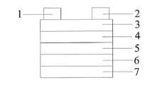
图1为本发明的有机场效应晶体管的结构示意图;其中,1为源电极,2为漏电极,3为有机半导体层,4为混合聚合物修饰层,5为介电层,6为栅电极,7为衬底。Fig. 1 is the structural representation of organic field effect transistor of the present invention; Wherein, 1 is source electrode, and 2 is drain electrode, and 3 is organic semiconductor layer, and 4 is mixed polymer modification layer, and 5 is dielectric layer, and 6 is gate electrode , 7 is the substrate.
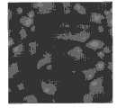
图2为聚苯乙烯修饰的介电层上并五苯形貌AFM图。Fig. 2 is an AFM image of the morphology of pentacene on the polystyrene-modified dielectric layer.
图3为聚苯醚修饰的介电层上并五苯形貌AFM图。Fig. 3 is an AFM image of the morphology of pentacene on the polyphenylene ether modified dielectric layer.
图4为未经凝胶色谱提纯的聚苯乙烯/聚苯醚共混介电层上(共混比例1∶1)并五苯形貌AFM图。Fig. 4 is an AFM image of the morphology of pentacene on the polystyrene/polyphenylene ether blended dielectric layer (blending ratio 1:1) without gel chromatography purification.
图5经凝胶色谱提纯的聚苯乙烯/聚苯醚共混修饰的介电层上(共混比例1∶1)并五苯形貌AFM图。Fig. 5 AFM image of the morphology of pentacene on the polystyrene/polyphenylene ether blended dielectric layer (blending ratio 1:1) purified by gel chromatography.
图6提纯与未提纯介电层共混比例与所对应的并五苯场效应晶体管迁移率。Fig. 6 The blend ratio of purified and unpurified dielectric layers and the corresponding mobility of pentacene field effect transistors.
图7未提纯介电层共混比例与所对应的并四苯场效应晶体管迁移率。Fig. 7 The blend ratio of the unpurified dielectric layer and the corresponding mobilities of naphthacene field effect transistors.
具体实施方式Detailed ways
本发明提供的高性能有机薄膜场效应晶体管为上电极结构,包括衬底、栅极电极、介电层、有机半导体层和源漏电极,结构如图1所示;其介电层为聚苯乙烯和聚苯醚共混物修饰的介电层。The high-performance organic thin-film field-effect transistor provided by the present invention is an upper electrode structure, including a substrate, a gate electrode, a dielectric layer, an organic semiconductor layer and a source-drain electrode, and the structure is as shown in Figure 1; its dielectric layer is polyphenylene Ethylene and polyphenylene ether blend modified dielectric layer.
制备所述的有机场效应晶体管的方法,包括以下步骤:The method for preparing the described organic field effect transistor comprises the following steps:
第一步,聚合物层的制备:The first step, the preparation of the polymer layer:
将沉积有栅极电极和介电层的衬底,依次用去离子水、乙醇、丙酮超声清洗后烘箱烘干,然后用甩膜的方法将聚合物混合溶液旋涂于绝缘层的表面,放入烘箱,抽真空加热退火处理;The substrate deposited with the gate electrode and the dielectric layer was ultrasonically cleaned with deionized water, ethanol, and acetone in sequence, and then dried in an oven. into the oven, vacuum heating and annealing treatment;
第二步,有机半导体材料的沉积:The second step, the deposition of organic semiconductor materials:
在上述修饰的衬底上采用有机物成膜方法制备厚度为30~60纳米的有机半导体层;An organic semiconductor layer with a thickness of 30-60 nanometers is prepared on the above-mentioned modified substrate by using an organic film-forming method;
第三步,源漏电极的制备:The third step, preparation of source and drain electrodes:
采用传统电极制备方法,真空沉积或者印刷金属作为源漏电极,得到有机场效应晶体管。The conventional electrode preparation method is used to vacuum deposit or print metal as the source and drain electrodes to obtain an organic field effect transistor.
下面通过具体实施例对本发明进行说明,但本发明并不局限于此。The present invention will be described below through specific examples, but the present invention is not limited thereto.
下述实施例中所述实验方法,如无特殊说明,均为常规方法;所述试剂和材料,如无特殊说明,均可从商业途径获得。The experimental methods described in the following examples, unless otherwise specified, are conventional methods; the reagents and materials, unless otherwise specified, can be obtained from commercial sources.
实施例1、聚苯乙烯/聚苯醚共混聚合物层并五苯形貌的优化控制及高性能并五苯场效应晶体管的制备Example 1. Optimal control of the morphology of pentacene in the polystyrene/polyphenylene ether blend polymer layer and preparation of high-performance pentacene field-effect transistors
第一步,聚合物层的制备:The first step, the preparation of the polymer layer:
将沉积有栅极电极(高掺杂硅)和介电层(二氧化硅)的衬底(硅片)依次用去离子水、乙醇、丙酮超声清洗后烘箱烘干,待用。将5mg/mL的聚苯乙烯(重均分子量50kDa)氯仿溶液和5mg/mL的聚苯醚(重均分子量为50kDa)氯仿溶液按体积比1∶1的比例共混,搅拌15min左右,然后用匀胶机甩膜将混合溶液,以2000r/min的转速旋涂于介电层表面,放入烘箱,抽真空,真空度为0.1帕斯卡,加热到80度处理1小时,自然冷却。聚合物层厚度为30nm。The substrate (silicon wafer) on which the gate electrode (highly doped silicon) and the dielectric layer (silicon dioxide) are deposited is ultrasonically cleaned with deionized water, ethanol, and acetone in sequence, and then dried in an oven for use.
第二步,有机半导体材料的沉积:The second step, the deposition of organic semiconductor materials:
将上述修饰的衬底放入真空镀膜机中,将真空度抽至为5×10⁻⁴Pa下,采用热蒸镀的方式,以0.8埃每秒的速度沉积并五苯有机层,至厚度为50纳米。Put the above-mentioned modified substrate into a vacuum coating machine, pump the vacuum to 5×10⁻⁴ Pa, and use thermal evaporation to deposit a pentacene organic layer at a rate of 0.8 angstroms per second to a thickness of is 50 nm.
第三步,源漏电极的制备:The third step, preparation of source and drain electrodes:
将金属掩模板盖在第二步中制备的并五苯有机薄膜上,放入真空镀膜机中,将真空度抽至为5×10⁻⁴Pa下,然后加热蒸发源上的金,使其以1埃每秒的速度沉积到盖有掩模的有机薄膜上,形成厚度为40纳米的金层作为源漏电极,得到有机场效应晶体管。Cover the metal mask on the pentacene organic film prepared in the second step, put it into a vacuum coating machine, and evacuate the vacuum to 5×10⁻⁴ Pa, and then heat the gold on the evaporation source to make it Deposit it on the organic film covered with a mask at a rate of 1 angstrom per second to form a gold layer with a thickness of 40 nanometers as the source and drain electrodes to obtain an organic field effect transistor.
第四步,形貌的控制与器件测试:The fourth step, morphology control and device testing:
试验发现,单独以聚苯乙烯为介电修饰层,通过AFM图可以看出,并五苯在聚苯乙烯上生成较小晶粒形貌(见图2),这种形貌晶粒间接触较好,但半导体薄膜的长程有序性较差。而单独以聚苯醚为介电修饰层,通过AFM图可以看出,并五苯在聚苯醚上形成较大晶粒形貌(见图3),与图2相反,这种形貌有着较好的长程有序性但晶粒之间的接触较差。而聚苯乙烯和聚苯醚共混物介电修饰层则诱导并五苯形成了一种由不同大小晶粒构成的织态结构(见图4),这种形貌结合了图2、图3所示形貌的优点,因而更有利于载流子传输。场效应器件迁移率达到2.2cm2/Vs(见图6),开关比为108。The test found that using polystyrene alone as the dielectric modification layer, it can be seen from the AFM image that pentacene generates smaller grain morphology on polystyrene (see Figure 2), and the contact between grains of this morphology Better, but the long-range order of semiconductor thin films is poor. However, using polyphenylene ether as the dielectric modification layer alone, it can be seen from the AFM image that pentacene forms a larger grain morphology on the polyphenylene ether (see Figure 3). Contrary to Figure 2, this morphology has Better long-range order but poor contact between grains. The polystyrene and polyphenylene ether blend dielectric modification layer induces pentacene to form a textured structure composed of grains of different sizes (see Figure 4). This morphology combines Figure 2 and Figure 4. The advantages of the morphology shown in 3 are thus more conducive to carrier transport. The field effect device has a mobility of 2.2cm2 /Vs (see Figure 6), and an on/off ratio of 108 .
迁移率和开关比的具体测定方法如下:在室温下用Keithley 4200半导体测试仪测量了所制备的有机场效应晶体管的电性质。决定OFET器件性能的两个关键参数是:载流子的迁移率(μ)和器件的开关比(Ion/Ioff)。迁移率是指:在单位电场下,载流子的平均漂移速度(单位是cm2/V·s),它反映了在电场下空穴或电子在半导体中的迁移能力。开关比定义为:在一定的栅极电压下,晶体管在“开”状态和“关”状态下的电流之比,它反映了器件开关性能的优劣。The specific measurement methods of the mobility and the on-off ratio are as follows: the electrical properties of the prepared organic field effect transistor were measured at room temperature with a Keithley 4200 semiconductor tester. Two key parameters that determine the performance of OFET devices are: carrier mobility (μ) and device on/off ratio (Ion /Ioff ). Mobility refers to the average carrier drift velocity (unit: cm2 /V·s) under a unit electric field, which reflects the mobility of holes or electrons in a semiconductor under an electric field. The switching ratio is defined as: under a certain gate voltage, the ratio of the current of the transistor in the "on" state and the "off" state, which reflects the switching performance of the device.
载流子迁移率可由方程计算得出:The carrier mobility can be calculated from the equation:
IDS=(W/2L)Ciμ(VG-VT)2(饱和区,VDS=VG-VT)IDS =(W/2L)Ci μ(VG -VT )2 (saturation region, VDS =VG -VT )
其中,IDS为漏极电流,μ为载流子迁移率,VG为栅极电压,VT为阈值电压,W为沟道宽度(W=3mm),L为沟道长度(L=0.05mm),Ci为绝缘体电容(Ci=7.5×10⁻⁹F/cm2)。利用(IDS,sat)1/2对VG作图,并作线性回归,可由此回归线的斜率推算出载流子迁移率(μ),由回归线与X轴的截点求得VT。迁移率可以根据公式从转移曲线的斜率计算得出。开关比可由源漏电流的最大值与最小值之比得出。Among them, IDS is the drain current, μ is the carrier mobility, VG is the gate voltage, VT is the threshold voltage, W is the channel width (W=3mm), L is the channel length (L=0.05 mm), Ci is the insulator capacitance (Ci =7.5×10⁻⁹ F/cm2 ). Use (IDDS , sat)1/2 to plot VG and perform linear regression. The carrier mobility (μ) can be calculated from the slope of the regression line, and VT can be obtained from the intercept point of the regression line and the X-axis. Mobility can be calculated from the slope of the transfer curve according to the formula. The on-off ratio can be obtained from the ratio of the maximum value to the minimum value of the source-drain current.
在上述实施例中将聚苯乙烯替换为重均分子量为13kDa,25kDa,30kDa,200kDa,650kDa聚苯乙烯,所制备的器件性能无明显变化。将聚苯醚替换为重均分子量为20kDa和600kDa的聚苯醚,所制备的器件性能也无明显变化。聚合物层厚度在10-50nm范围内,所制备的器件性能也无明显变化。In the above examples, polystyrene is replaced by polystyrene with a weight average molecular weight of 13kDa, 25kDa, 30kDa, 200kDa, 650kDa, and the performance of the prepared device has no obvious change. The performance of the prepared devices did not change significantly when the polyphenylene ether was replaced by polyphenylene ether with a weight average molecular weight of 20kDa and 600kDa. When the thickness of the polymer layer is in the range of 10-50nm, the performance of the prepared device has no obvious change.
实施例2、基于凝胶色谱提纯后的聚苯乙烯/聚苯醚共混聚合物介电修饰层的并五苯有机场效应晶体管Example 2. Pentacene Organic Field Effect Transistor Based on Dielectric Modification Layer of Polystyrene/Polyphenylene Ether Blend Polymer Purified by Gel Chromatography
器件的制备和测试方法与实施例1基本一致,唯一不同的是本实施例所采用的聚苯乙烯和聚苯醚通过凝胶色谱进行了提纯。具体提纯方法如下:将聚苯乙烯(或聚苯醚)溶液倒入凝胶色谱仪,通过仪器检测分子量的同时保留分子量为13kDa-650kDa范围的淋出级分(聚苯醚保留分子量为20kDa-600kDa的淋出级分),之后将所得溶液用旋转蒸发仪蒸干得到提纯样品。此过程有助于除掉聚合物中分子量在13kDa以下的小分子杂质和分子量巨大的团聚颗粒(>650kDa)。The preparation and testing methods of the device are basically the same as in Example 1, the only difference is that the polystyrene and polyphenylene ether used in this example are purified by gel chromatography. The specific purification method is as follows: pour the polystyrene (or polyphenylene ether) solution into a gel chromatograph, and retain the leaching fraction with a molecular weight of 13kDa-650kDa while detecting the molecular weight through the instrument (the polyphenylene ether retains a molecular weight of 20kDa-650kDa). 600kDa eluted fraction), and then the resulting solution was evaporated to dryness with a rotary evaporator to obtain a purified sample. This process helps to remove small molecular impurities with a molecular weight below 13kDa and agglomerated particles with a large molecular weight (>650kDa) in the polymer.
结果表明,在提纯后的聚苯乙烯和聚苯醚共混聚合物修饰层上形成的并五苯晶膜更加完善(见图5),场效应晶体管迁移率进一步提高到3.6cm2/Vs(见图6),开关比为108。The results show that the pentacene crystal film formed on the modified polystyrene and polyphenylene ether blended polymer layer is more complete (see Figure 5), and the mobility of the field effect transistor is further increased to 3.6cm2 /Vs ( See Fig. 6), the on-off ratio is 108 .
实施例3、基于聚苯乙烯/聚苯醚共混聚合物介电修饰层的并四苯场效应晶体管的制备Example 3. Preparation of tetracene field-effect transistor based on polystyrene/polyphenylene ether blend polymer dielectric modification layer
器件的制备和测试方法与实施例1基本一致,唯一不同的是本实施例使用并四苯作为半导体层。我们发现在未提纯的聚苯乙烯/聚苯醚共混介电修饰层上制备的并四苯场效应晶体管有着与并五苯场效应晶体管相似的性能提高规律,在聚苯乙烯/聚苯醚质量比1∶1共混比例的介电修饰层上,场效应晶体管迁移率提高到0.93cm2/Vs(见图7),开关比为107。The preparation and testing methods of the device are basically the same as in Example 1, the only difference is that tetracene is used as the semiconductor layer in this example. We found that tetracene field-effect transistors prepared on unpurified polystyrene/polyphenylene ether blended dielectric modification layer have similar performance improvement laws as pentacene field-effect transistors. In polystyrene/polyphenylene ether On the dielectric modification layer with a mass ratio of 1:1, the mobility of the field effect transistor is increased to 0.93 cm2 /Vs (see FIG. 7 ), and the on/off ratio is 107 .
Claims (10)
Translated fromChinesePriority Applications (1)
| Application Number | Priority Date | Filing Date | Title |
|---|---|---|---|
| CN201010578898ACN102110776B (en) | 2010-12-03 | 2010-12-03 | High-performance Organic field effect transistor and preparation method thereof |
Applications Claiming Priority (1)
| Application Number | Priority Date | Filing Date | Title |
|---|---|---|---|
| CN201010578898ACN102110776B (en) | 2010-12-03 | 2010-12-03 | High-performance Organic field effect transistor and preparation method thereof |
Publications (2)
| Publication Number | Publication Date |
|---|---|
| CN102110776Atrue CN102110776A (en) | 2011-06-29 |
| CN102110776B CN102110776B (en) | 2012-10-03 |
Family
ID=44174863
Family Applications (1)
| Application Number | Title | Priority Date | Filing Date |
|---|---|---|---|
| CN201010578898AExpired - Fee RelatedCN102110776B (en) | 2010-12-03 | 2010-12-03 | High-performance Organic field effect transistor and preparation method thereof |
Country Status (1)
| Country | Link |
|---|---|
| CN (1) | CN102110776B (en) |
Cited By (12)
| Publication number | Priority date | Publication date | Assignee | Title |
|---|---|---|---|---|
| CN102420288A (en)* | 2011-11-21 | 2012-04-18 | 北京科技大学 | Organic field effect transistor with dielectric modification layer and preparation method |
| CN104415453A (en)* | 2013-08-22 | 2015-03-18 | 上海中医药大学附属龙华医院 | Directional conductive acupuncture needle and preparation method thereof |
| CN104849336A (en)* | 2015-04-22 | 2015-08-19 | 电子科技大学 | Organic field effect transistor gas sensor and preparation method thereof |
| CN106876585A (en)* | 2017-01-19 | 2017-06-20 | 南京邮电大学 | A kind of method that organic field effect tube mobility is improved by short annealing |
| CN108287189A (en)* | 2018-01-03 | 2018-07-17 | 电子科技大学 | A kind of organic field effect tube humidity sensor based on synergistic effect and preparation method thereof |
| CN111554670A (en)* | 2020-05-18 | 2020-08-18 | 济南大学 | Flexible Smart Piezoelectric Sensor Based on Pentacene Organic Field Effect Transistor Coupled with PVDF Nanopillars |
| CN112490362A (en)* | 2020-11-11 | 2021-03-12 | 西安理工大学 | Preparation method of organic field effect transistor based on patterned substrate |
| CN112694388A (en)* | 2019-10-22 | 2021-04-23 | 中国科学院化学研究所 | Naphthacene derivative and preparation method and application thereof |
| CN113410384A (en)* | 2021-06-28 | 2021-09-17 | 西南大学 | Preparation method of polymer dielectric layer for flexible field effect transistor |
| WO2021208077A1 (en)* | 2020-04-17 | 2021-10-21 | 北京大学深圳研究生院 | Organic field effect transistor and manufacturing method therefor |
| CN114497372A (en)* | 2021-12-29 | 2022-05-13 | 闽都创新实验室 | A kind of low power consumption field effect transistor and preparation method thereof |
| US11937438B2 (en) | 2020-04-17 | 2024-03-19 | Peking University Shenzhen Graduate School | Organic field-effect transistor and fabrication method therefor |
Citations (8)
| Publication number | Priority date | Publication date | Assignee | Title |
|---|---|---|---|---|
| WO2005086254A1 (en)* | 2004-03-10 | 2005-09-15 | Canon Kabushiki Kaisha | Field effect transistor, method of producing the same, and method of producing laminated member |
| CN1698217A (en)* | 2001-12-19 | 2005-11-16 | 艾夫西亚有限公司 | Organic Field Effect Transistors Using Organic Dielectrics |
| CN101162761A (en)* | 2006-10-13 | 2008-04-16 | 中国科学院化学研究所 | Method for realizing low voltage operating organic field effect transistor |
| US7435989B2 (en)* | 2005-09-06 | 2008-10-14 | Canon Kabushiki Kaisha | Semiconductor device with layer containing polysiloxane compound |
| CN101295765A (en)* | 2008-06-19 | 2008-10-29 | 中国科学院化学研究所 | A kind of organic field effect transistor and its preparation method and application |
| CN101339975A (en)* | 2008-08-12 | 2009-01-07 | 中国科学院化学研究所 | A kind of organic field effect transistor with high mobility and its preparation method |
| US7511296B2 (en)* | 2005-03-25 | 2009-03-31 | Canon Kabushiki Kaisha | Organic semiconductor device, field-effect transistor, and their manufacturing methods |
| JP2010056408A (en)* | 2008-08-29 | 2010-03-11 | Hitachi Chem Co Ltd | Aluminum-containing organic compound solution, field-effect transistor, and method of manufacturing field-effect transistor |
- 2010
- 2010-12-03CNCN201010578898Apatent/CN102110776B/ennot_activeExpired - Fee Related
Patent Citations (8)
| Publication number | Priority date | Publication date | Assignee | Title |
|---|---|---|---|---|
| CN1698217A (en)* | 2001-12-19 | 2005-11-16 | 艾夫西亚有限公司 | Organic Field Effect Transistors Using Organic Dielectrics |
| WO2005086254A1 (en)* | 2004-03-10 | 2005-09-15 | Canon Kabushiki Kaisha | Field effect transistor, method of producing the same, and method of producing laminated member |
| US7511296B2 (en)* | 2005-03-25 | 2009-03-31 | Canon Kabushiki Kaisha | Organic semiconductor device, field-effect transistor, and their manufacturing methods |
| US7435989B2 (en)* | 2005-09-06 | 2008-10-14 | Canon Kabushiki Kaisha | Semiconductor device with layer containing polysiloxane compound |
| CN101162761A (en)* | 2006-10-13 | 2008-04-16 | 中国科学院化学研究所 | Method for realizing low voltage operating organic field effect transistor |
| CN101295765A (en)* | 2008-06-19 | 2008-10-29 | 中国科学院化学研究所 | A kind of organic field effect transistor and its preparation method and application |
| CN101339975A (en)* | 2008-08-12 | 2009-01-07 | 中国科学院化学研究所 | A kind of organic field effect transistor with high mobility and its preparation method |
| JP2010056408A (en)* | 2008-08-29 | 2010-03-11 | Hitachi Chem Co Ltd | Aluminum-containing organic compound solution, field-effect transistor, and method of manufacturing field-effect transistor |
Cited By (17)
| Publication number | Priority date | Publication date | Assignee | Title |
|---|---|---|---|---|
| CN102420288B (en)* | 2011-11-21 | 2013-07-03 | 北京科技大学 | Organic field effect transistor with dielectric modification layer and preparation method thereof |
| CN102420288A (en)* | 2011-11-21 | 2012-04-18 | 北京科技大学 | Organic field effect transistor with dielectric modification layer and preparation method |
| CN104415453A (en)* | 2013-08-22 | 2015-03-18 | 上海中医药大学附属龙华医院 | Directional conductive acupuncture needle and preparation method thereof |
| CN104849336A (en)* | 2015-04-22 | 2015-08-19 | 电子科技大学 | Organic field effect transistor gas sensor and preparation method thereof |
| CN104849336B (en)* | 2015-04-22 | 2018-01-19 | 电子科技大学 | Organic field effect tube gas sensor and preparation method thereof |
| CN106876585A (en)* | 2017-01-19 | 2017-06-20 | 南京邮电大学 | A kind of method that organic field effect tube mobility is improved by short annealing |
| CN108287189A (en)* | 2018-01-03 | 2018-07-17 | 电子科技大学 | A kind of organic field effect tube humidity sensor based on synergistic effect and preparation method thereof |
| CN108287189B (en)* | 2018-01-03 | 2019-12-03 | 电子科技大学 | A kind of organic field effect tube humidity sensor based on synergistic effect and preparation method thereof |
| CN112694388A (en)* | 2019-10-22 | 2021-04-23 | 中国科学院化学研究所 | Naphthacene derivative and preparation method and application thereof |
| WO2021208077A1 (en)* | 2020-04-17 | 2021-10-21 | 北京大学深圳研究生院 | Organic field effect transistor and manufacturing method therefor |
| US11937438B2 (en) | 2020-04-17 | 2024-03-19 | Peking University Shenzhen Graduate School | Organic field-effect transistor and fabrication method therefor |
| CN111554670A (en)* | 2020-05-18 | 2020-08-18 | 济南大学 | Flexible Smart Piezoelectric Sensor Based on Pentacene Organic Field Effect Transistor Coupled with PVDF Nanopillars |
| CN111554670B (en)* | 2020-05-18 | 2022-03-29 | 济南大学 | Flexible intelligent piezoelectric sensor based on coupling of pentacene organic field effect transistor and PVDF (polyvinylidene fluoride) nano-column |
| CN112490362A (en)* | 2020-11-11 | 2021-03-12 | 西安理工大学 | Preparation method of organic field effect transistor based on patterned substrate |
| CN113410384A (en)* | 2021-06-28 | 2021-09-17 | 西南大学 | Preparation method of polymer dielectric layer for flexible field effect transistor |
| CN113410384B (en)* | 2021-06-28 | 2023-04-07 | 西南大学 | Preparation method of polymer dielectric layer for flexible field effect transistor |
| CN114497372A (en)* | 2021-12-29 | 2022-05-13 | 闽都创新实验室 | A kind of low power consumption field effect transistor and preparation method thereof |
Also Published As
| Publication number | Publication date |
|---|---|
| CN102110776B (en) | 2012-10-03 |
Similar Documents
| Publication | Publication Date | Title |
|---|---|---|
| CN102110776A (en) | High-performance Organic field effect transistor and preparation method thereof | |
| Lee et al. | Solution-processed zinc–tin oxide thin-film transistors with low interfacial trap density and improved performance | |
| CN101442105B (en) | An organic field effect transistor, its special source and drain electrodes and its preparation method | |
| CN103700710B (en) | IGZO thin film transistor (TFT)s and preparation method thereof | |
| Bukke et al. | Remarkable increase in field effect mobility of amorphous IZTO thin-film transistors with purified ZrO x gate insulator | |
| CN110265548A (en) | A kind of indium-doped N-type organic thin film transistor and its preparation method | |
| Spalenka et al. | Electron mobility enhancement in ZnO thin films via surface modification by carboxylic acids | |
| KR20140081249A (en) | Oxide Thin-Film Transistor Comprising Self-Assembly Monolayer and Method for Preparation thereof | |
| CN100593871C (en) | A kind of organic field effect transistor with high mobility and its preparation method | |
| CN101101967A (en) | Low-cost high-performance organic field effect transistor and its preparation method | |
| CN109638158A (en) | A kind of flexible organic film transistor and preparation method thereof | |
| Oh et al. | Low-voltage pentacene thin-film transistors using Hf-based blend gate dielectrics | |
| Liu et al. | High performance and high yield solution processed IGZO thin film transistors fabricated with low‐temperature annealed hafnium dioxide gate dielectric | |
| Liu et al. | Low-voltage-operation of flexible organic C8-BTBT thin-film transistors with a reactively sputtered AlOx gate dielectric | |
| Liu et al. | High-performance n-and p-type organic single-crystal field-effect transistors with an air-gap dielectric towards anti-ambipolar transport | |
| CN102222766A (en) | C60 organic field effect transistor with hydroxyquinoline aluminium as modification layer | |
| Li et al. | A novel TFT with organic-inorganic hybrid perovskite channel layer | |
| Zhang et al. | Full-solution-processed high mobility zinc-tin-oxide thin-film-transistors | |
| CN101425562B (en) | A nanoscale channel organic field effect transistor and its preparation method | |
| CN110112293A (en) | A kind of high molecular polymer thin film transistor (TFT) and preparation method thereof | |
| CN100421279C (en) | Organic thin film transistor device containing modification layer and its processing method | |
| CN102208364B (en) | Large-area organic thin film transistor array preparation method compatible with roll-to-roll technology | |
| Omprakash et al. | Fabrication of flexible metal oxide thin film transistor by indigenously developed spray pyrolysis unit | |
| Sun et al. | Polymer gate dielectrics with self-assembled monolayers for high-mobility organic thin-film transistors based on copper phthalocyanine | |
| CN107731909A (en) | Based on MoO3/Al2O3The diamond field effect transistor and preparation method of double layer gate dielectric |
Legal Events
| Date | Code | Title | Description |
|---|---|---|---|
| C06 | Publication | ||
| PB01 | Publication | ||
| C10 | Entry into substantive examination | ||
| SE01 | Entry into force of request for substantive examination | ||
| C14 | Grant of patent or utility model | ||
| GR01 | Patent grant | ||
| CF01 | Termination of patent right due to non-payment of annual fee | Granted publication date:20121003 Termination date:20151203 | |
| EXPY | Termination of patent right or utility model |