CN102104107B - Light emitting device - Google Patents
Light emitting deviceDownload PDFInfo
- Publication number
- CN102104107B CN102104107BCN2010102744342ACN201010274434ACN102104107BCN 102104107 BCN102104107 BCN 102104107BCN 2010102744342 ACN2010102744342 ACN 2010102744342ACN 201010274434 ACN201010274434 ACN 201010274434ACN 102104107 BCN102104107 BCN 102104107B
- Authority
- CN
- China
- Prior art keywords
- light
- layer
- wavelength conversion
- light emitting
- conversion layer
- Prior art date
- Legal status (The legal status is an assumption and is not a legal conclusion. Google has not performed a legal analysis and makes no representation as to the accuracy of the status listed.)
- Expired - Fee Related
Links
Images


Classifications
- H—ELECTRICITY
- H10—SEMICONDUCTOR DEVICES; ELECTRIC SOLID-STATE DEVICES NOT OTHERWISE PROVIDED FOR
- H10H—INORGANIC LIGHT-EMITTING SEMICONDUCTOR DEVICES HAVING POTENTIAL BARRIERS
- H10H20/00—Individual inorganic light-emitting semiconductor devices having potential barriers, e.g. light-emitting diodes [LED]
- H10H20/80—Constructional details
- H10H20/85—Packages
- H10H20/851—Wavelength conversion means
- H—ELECTRICITY
- H01—ELECTRIC ELEMENTS
- H01L—SEMICONDUCTOR DEVICES NOT COVERED BY CLASS H10
- H01L24/00—Arrangements for connecting or disconnecting semiconductor or solid-state bodies; Methods or apparatus related thereto
- H01L24/01—Means for bonding being attached to, or being formed on, the surface to be connected, e.g. chip-to-package, die-attach, "first-level" interconnects; Manufacturing methods related thereto
- H01L24/26—Layer connectors, e.g. plate connectors, solder or adhesive layers; Manufacturing methods related thereto
- H01L24/28—Structure, shape, material or disposition of the layer connectors prior to the connecting process
- H01L24/29—Structure, shape, material or disposition of the layer connectors prior to the connecting process of an individual layer connector
- H—ELECTRICITY
- H01—ELECTRIC ELEMENTS
- H01L—SEMICONDUCTOR DEVICES NOT COVERED BY CLASS H10
- H01L24/00—Arrangements for connecting or disconnecting semiconductor or solid-state bodies; Methods or apparatus related thereto
- H01L24/01—Means for bonding being attached to, or being formed on, the surface to be connected, e.g. chip-to-package, die-attach, "first-level" interconnects; Manufacturing methods related thereto
- H01L24/26—Layer connectors, e.g. plate connectors, solder or adhesive layers; Manufacturing methods related thereto
- H01L24/31—Structure, shape, material or disposition of the layer connectors after the connecting process
- H01L24/32—Structure, shape, material or disposition of the layer connectors after the connecting process of an individual layer connector
- H—ELECTRICITY
- H10—SEMICONDUCTOR DEVICES; ELECTRIC SOLID-STATE DEVICES NOT OTHERWISE PROVIDED FOR
- H10H—INORGANIC LIGHT-EMITTING SEMICONDUCTOR DEVICES HAVING POTENTIAL BARRIERS
- H10H20/00—Individual inorganic light-emitting semiconductor devices having potential barriers, e.g. light-emitting diodes [LED]
- H10H20/80—Constructional details
- H10H20/85—Packages
- H10H20/851—Wavelength conversion means
- H10H20/8511—Wavelength conversion means characterised by their material, e.g. binder
- H10H20/8512—Wavelength conversion materials
- H10H20/8513—Wavelength conversion materials having two or more wavelength conversion materials
- H—ELECTRICITY
- H01—ELECTRIC ELEMENTS
- H01L—SEMICONDUCTOR DEVICES NOT COVERED BY CLASS H10
- H01L2224/00—Indexing scheme for arrangements for connecting or disconnecting semiconductor or solid-state bodies and methods related thereto as covered by H01L24/00
- H01L2224/01—Means for bonding being attached to, or being formed on, the surface to be connected, e.g. chip-to-package, die-attach, "first-level" interconnects; Manufacturing methods related thereto
- H01L2224/10—Bump connectors; Manufacturing methods related thereto
- H01L2224/15—Structure, shape, material or disposition of the bump connectors after the connecting process
- H01L2224/16—Structure, shape, material or disposition of the bump connectors after the connecting process of an individual bump connector
- H01L2224/161—Disposition
- H01L2224/16151—Disposition the bump connector connecting between a semiconductor or solid-state body and an item not being a semiconductor or solid-state body, e.g. chip-to-substrate, chip-to-passive
- H01L2224/16221—Disposition the bump connector connecting between a semiconductor or solid-state body and an item not being a semiconductor or solid-state body, e.g. chip-to-substrate, chip-to-passive the body and the item being stacked
- H01L2224/16225—Disposition the bump connector connecting between a semiconductor or solid-state body and an item not being a semiconductor or solid-state body, e.g. chip-to-substrate, chip-to-passive the body and the item being stacked the item being non-metallic, e.g. insulating substrate with or without metallisation
- H—ELECTRICITY
- H01—ELECTRIC ELEMENTS
- H01L—SEMICONDUCTOR DEVICES NOT COVERED BY CLASS H10
- H01L2224/00—Indexing scheme for arrangements for connecting or disconnecting semiconductor or solid-state bodies and methods related thereto as covered by H01L24/00
- H01L2224/01—Means for bonding being attached to, or being formed on, the surface to be connected, e.g. chip-to-package, die-attach, "first-level" interconnects; Manufacturing methods related thereto
- H01L2224/26—Layer connectors, e.g. plate connectors, solder or adhesive layers; Manufacturing methods related thereto
- H01L2224/31—Structure, shape, material or disposition of the layer connectors after the connecting process
- H01L2224/32—Structure, shape, material or disposition of the layer connectors after the connecting process of an individual layer connector
- H01L2224/321—Disposition
- H01L2224/32151—Disposition the layer connector connecting between a semiconductor or solid-state body and an item not being a semiconductor or solid-state body, e.g. chip-to-substrate, chip-to-passive
- H01L2224/32221—Disposition the layer connector connecting between a semiconductor or solid-state body and an item not being a semiconductor or solid-state body, e.g. chip-to-substrate, chip-to-passive the body and the item being stacked
- H01L2224/32225—Disposition the layer connector connecting between a semiconductor or solid-state body and an item not being a semiconductor or solid-state body, e.g. chip-to-substrate, chip-to-passive the body and the item being stacked the item being non-metallic, e.g. insulating substrate with or without metallisation
- H—ELECTRICITY
- H01—ELECTRIC ELEMENTS
- H01L—SEMICONDUCTOR DEVICES NOT COVERED BY CLASS H10
- H01L2224/00—Indexing scheme for arrangements for connecting or disconnecting semiconductor or solid-state bodies and methods related thereto as covered by H01L24/00
- H01L2224/01—Means for bonding being attached to, or being formed on, the surface to be connected, e.g. chip-to-package, die-attach, "first-level" interconnects; Manufacturing methods related thereto
- H01L2224/42—Wire connectors; Manufacturing methods related thereto
- H01L2224/47—Structure, shape, material or disposition of the wire connectors after the connecting process
- H01L2224/48—Structure, shape, material or disposition of the wire connectors after the connecting process of an individual wire connector
- H01L2224/4805—Shape
- H01L2224/4809—Loop shape
- H01L2224/48091—Arched
- H—ELECTRICITY
- H01—ELECTRIC ELEMENTS
- H01L—SEMICONDUCTOR DEVICES NOT COVERED BY CLASS H10
- H01L2224/00—Indexing scheme for arrangements for connecting or disconnecting semiconductor or solid-state bodies and methods related thereto as covered by H01L24/00
- H01L2224/01—Means for bonding being attached to, or being formed on, the surface to be connected, e.g. chip-to-package, die-attach, "first-level" interconnects; Manufacturing methods related thereto
- H01L2224/42—Wire connectors; Manufacturing methods related thereto
- H01L2224/47—Structure, shape, material or disposition of the wire connectors after the connecting process
- H01L2224/48—Structure, shape, material or disposition of the wire connectors after the connecting process of an individual wire connector
- H01L2224/481—Disposition
- H01L2224/48151—Connecting between a semiconductor or solid-state body and an item not being a semiconductor or solid-state body, e.g. chip-to-substrate, chip-to-passive
- H01L2224/48221—Connecting between a semiconductor or solid-state body and an item not being a semiconductor or solid-state body, e.g. chip-to-substrate, chip-to-passive the body and the item being stacked
- H01L2224/48225—Connecting between a semiconductor or solid-state body and an item not being a semiconductor or solid-state body, e.g. chip-to-substrate, chip-to-passive the body and the item being stacked the item being non-metallic, e.g. insulating substrate with or without metallisation
- H01L2224/48227—Connecting between a semiconductor or solid-state body and an item not being a semiconductor or solid-state body, e.g. chip-to-substrate, chip-to-passive the body and the item being stacked the item being non-metallic, e.g. insulating substrate with or without metallisation connecting the wire to a bond pad of the item
- H—ELECTRICITY
- H01—ELECTRIC ELEMENTS
- H01L—SEMICONDUCTOR DEVICES NOT COVERED BY CLASS H10
- H01L2224/00—Indexing scheme for arrangements for connecting or disconnecting semiconductor or solid-state bodies and methods related thereto as covered by H01L24/00
- H01L2224/01—Means for bonding being attached to, or being formed on, the surface to be connected, e.g. chip-to-package, die-attach, "first-level" interconnects; Manufacturing methods related thereto
- H01L2224/42—Wire connectors; Manufacturing methods related thereto
- H01L2224/47—Structure, shape, material or disposition of the wire connectors after the connecting process
- H01L2224/49—Structure, shape, material or disposition of the wire connectors after the connecting process of a plurality of wire connectors
- H01L2224/491—Disposition
- H01L2224/49105—Connecting at different heights
- H01L2224/49107—Connecting at different heights on the semiconductor or solid-state body
- H—ELECTRICITY
- H01—ELECTRIC ELEMENTS
- H01L—SEMICONDUCTOR DEVICES NOT COVERED BY CLASS H10
- H01L2224/00—Indexing scheme for arrangements for connecting or disconnecting semiconductor or solid-state bodies and methods related thereto as covered by H01L24/00
- H01L2224/73—Means for bonding being of different types provided for in two or more of groups H01L2224/10, H01L2224/18, H01L2224/26, H01L2224/34, H01L2224/42, H01L2224/50, H01L2224/63, H01L2224/71
- H01L2224/732—Location after the connecting process
- H01L2224/73251—Location after the connecting process on different surfaces
- H01L2224/73265—Layer and wire connectors
- H—ELECTRICITY
- H01—ELECTRIC ELEMENTS
- H01L—SEMICONDUCTOR DEVICES NOT COVERED BY CLASS H10
- H01L2924/00—Indexing scheme for arrangements or methods for connecting or disconnecting semiconductor or solid-state bodies as covered by H01L24/00
- H01L2924/15—Details of package parts other than the semiconductor or other solid state devices to be connected
- H01L2924/181—Encapsulation
- H—ELECTRICITY
- H10—SEMICONDUCTOR DEVICES; ELECTRIC SOLID-STATE DEVICES NOT OTHERWISE PROVIDED FOR
- H10H—INORGANIC LIGHT-EMITTING SEMICONDUCTOR DEVICES HAVING POTENTIAL BARRIERS
- H10H20/00—Individual inorganic light-emitting semiconductor devices having potential barriers, e.g. light-emitting diodes [LED]
- H10H20/80—Constructional details
- H10H20/84—Coatings, e.g. passivation layers or antireflective coatings
- H—ELECTRICITY
- H10—SEMICONDUCTOR DEVICES; ELECTRIC SOLID-STATE DEVICES NOT OTHERWISE PROVIDED FOR
- H10H—INORGANIC LIGHT-EMITTING SEMICONDUCTOR DEVICES HAVING POTENTIAL BARRIERS
- H10H20/00—Individual inorganic light-emitting semiconductor devices having potential barriers, e.g. light-emitting diodes [LED]
- H10H20/80—Constructional details
- H10H20/85—Packages
- H10H20/855—Optical field-shaping means, e.g. lenses
Landscapes
- Engineering & Computer Science (AREA)
- Computer Hardware Design (AREA)
- Microelectronics & Electronic Packaging (AREA)
- Power Engineering (AREA)
- Led Device Packages (AREA)
- Led Devices (AREA)
Abstract
Translated fromChinese
Description
Translated fromChinese相关申请的交叉引用Cross References to Related Applications
本申请基于并要求2009年12月22日提交的在先的日本专利申请2009-290554的优先权,在此引入其整个内容作为参考。This application is based upon and claims priority from prior Japanese Patent Application No. 2009-290554 filed on December 22, 2009, the entire contents of which are incorporated herein by reference.
技术领域technical field
在此说明的实施例一般而言涉及发光器件。Embodiments described herein relate generally to light emitting devices.
背景技术Background technique
通过组合荧光剂与诸如蓝光LED的半导体发光元件而发射白光的白光LED发光器件已被开发作为具有低功率消耗的小发光器件。White LED light emitting devices that emit white light by combining phosphors with semiconductor light emitting elements such as blue LEDs have been developed as small light emitting devices with low power consumption.
JP-A 2001-210874(特开)公开了这样一种结构,其中将包括衬底和预先设置在衬底下面上的荧光剂层的LED芯片安装在引线框上,并将荧光剂涂覆到LED芯片的表面上。然而,这样的结构不能充分提高效率。此外,由于在LED芯片与引线框之间设置有荧光剂层和管芯接合粘合剂,散热性差;由于发热,发光效能降低;并且可靠性不希望地降低。JP-A 2001-210874 (Kokai) discloses a structure in which an LED chip comprising a substrate and a phosphor layer preliminarily placed on the underside of the substrate is mounted on a lead frame, and the phosphor is applied to on the surface of the LED chip. However, such a structure cannot sufficiently improve efficiency. In addition, since the phosphor layer and the die-bonding adhesive are disposed between the LED chip and the lead frame, heat dissipation is poor; luminous efficacy is lowered due to heat generation; and reliability is undesirably lowered.
虽然对更高效率的发光器件的需求日益增加,但通过常规技术不能充分地提高效率。Although there is an increasing demand for higher-efficiency light-emitting devices, the efficiency cannot be sufficiently improved by conventional techniques.
发明内容Contents of the invention
总的来说,根据一个实施例,一种发光器件包括半导体发光元件、安装构件、第一波长转换层、第二波长转换层、以及第一透明层。所述半导体发光元件发射第一光。所述半导体发光元件被设置在所述安装构件上。所述第一波长转换层被设置在所述半导体发光元件与所述安装构件之间且与所述安装构件接触。所述第一波长转换层吸收所发射的所述第一光并发射第二光,所述第二光的波长大于所述第一光的波长。所述半导体发光元件被设置在所述第二波长转换层的至少一部分与所述第一波长转换层之间。所述第二波长转换层吸收所述第一光并发射第三光,所述第三光的波长大于所述第一光的波长。所述第一透明层被设置在所述半导体发光元件与所述第二波长转换层之间。所述第一透明层对所述第一光、所述第二光和所述第三光透明。In general, according to one embodiment, a light emitting device includes a semiconductor light emitting element, a mounting member, a first wavelength conversion layer, a second wavelength conversion layer, and a first transparent layer. The semiconductor light emitting element emits first light. The semiconductor light emitting element is provided on the mounting member. The first wavelength conversion layer is provided between the semiconductor light emitting element and the mounting member and is in contact with the mounting member. The first wavelength converting layer absorbs the emitted first light and emits second light having a wavelength greater than that of the first light. The semiconductor light emitting element is provided between at least a part of the second wavelength conversion layer and the first wavelength conversion layer. The second wavelength conversion layer absorbs the first light and emits third light having a wavelength greater than that of the first light. The first transparent layer is provided between the semiconductor light emitting element and the second wavelength conversion layer. The first transparent layer is transparent to the first light, the second light, and the third light.
附图说明Description of drawings
图1是示例出发光器件的示意性截面图;1 is a schematic cross-sectional view illustrating a light emitting device;
图2是在发光器件中使用的半导体发光元件的示意性截面图;2 is a schematic cross-sectional view of a semiconductor light emitting element used in a light emitting device;
图3是示例出发光器件的操作的示意图;3 is a schematic diagram illustrating the operation of a light emitting device;
图4是示例出比较例的发光器件的示意性截面图;4 is a schematic cross-sectional view illustrating a light emitting device of a comparative example;
图5是示例出比较例的发光器件的示意性截面图;5 is a schematic cross-sectional view illustrating a light emitting device of a comparative example;
图6是示例出比较例的发光器件的示意性截面图;6 is a schematic cross-sectional view illustrating a light emitting device of a comparative example;
图7是示例出比较例的发光器件的示意性截面图;7 is a schematic cross-sectional view illustrating a light emitting device of a comparative example;
图8是示例出发光器件的示意性截面图;8 is a schematic cross-sectional view illustrating a light emitting device;
图9是示例出发光器件的操作的示意图;9 is a schematic diagram illustrating the operation of a light emitting device;
图10A、图10B和图10C是示例出发光器件的示意性截面图;以及10A, 10B and 10C are schematic cross-sectional views illustrating a light emitting device; and
图11A和11B是示例出发光器件的示意性截面图。11A and 11B are schematic cross-sectional views illustrating a light emitting device.
具体实施方式Detailed ways
下面将参考附图更详细地说明本发明的示例性实施例。Exemplary embodiments of the present invention will be described in more detail below with reference to the accompanying drawings.
附图是示意性的或概念性的;并且各部分的厚度与宽度之间的关系、各部分之间的尺寸的比例等等未必与其实际值相同。此外,各附图之间,甚至对于相同的部分,尺寸和比例可以被不同地示例。The drawings are schematic or conceptual; and the relationship between the thickness and width of each part, the ratio of dimensions between the parts, etc. are not necessarily the same as their actual values. Also, dimensions and ratios may be illustrated differently between drawings, even for the same parts.
在本申请的说明书和附图中,用相似的参考标号标记与关于上述附图描述的内容相似的部件,并且在适当时省略详细的描述。In the specification and drawings of the present application, components similar to those described with respect to the above-mentioned drawings are marked with like reference numerals, and detailed descriptions are omitted where appropriate.
第一实施例first embodiment
图1是示例出根据本发明的第一实施例的发光器件的结构的示意性截面图。Fig. 1 is a schematic cross-sectional view illustrating the structure of a light emitting device according to a first embodiment of the present invention.
图2是示例出在根据本发明的第一实施例的发光器件中使用的半导体发光元件的结构的示意性截面图。Fig. 2 is a schematic cross-sectional view illustrating the structure of a semiconductor light emitting element used in a light emitting device according to a first embodiment of the present invention.
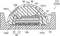
如图1所示,根据该实施例的发光器件210包括半导体发光元件10、安装构件20、第一波长转换层30、第二波长转换层80、以及第一透明层60。As shown in FIG. 1 , a
半导体发光元件10被设置在安装构件20上。第一波长转换层30被设置在半导体发光元件10与安装构件20之间且与安装构件20接触。第一波长转换层30吸收从半导体发光元件10发射的第一光并发射第二光,该第二光的波长大于第一光的波长。换言之,第二光的波长带大于第一光的波长带。例如,第二光的波长带的最小波长大于第一光的波长带的最小波长。例如,第二光的波长带的最大波长大于第一光的波长带的最大波长。例如,第二光的波长带的最小波长大于第一光的波长带的最大波长。例如,第二光的峰值波长大于第一光的峰值波长。The semiconductor
第二波长转换层80被设置在半导体发光元件10的与第一波长转换层30相反的一侧,吸收第一光。即,半导体发光元件10被设置在第二波长转换层80的至少一部分与第一波长转换层30之间。第二波长转换层80发射第三光,第三光的波长大于第一光的波长。换言之,第三光的波长带大于第一光的波长带。例如,第三光的波长带的最小波长大于第一光的波长带的最小波长。例如,第三光的波长带的最大波长大于第一光的波长带的最大波长。例如,第三光的波长带的最小波长大于第一光的波长带的最大波长。例如,第三光的峰值波长大于第一光的峰值波长。第三光可以具有与第二光的波长特性基本上相同或不同的波长特性。第二波长转换层80还吸收第二光;并且由此从第二波长转换层80发射的第三光可以具有与第一光和第二光的波长特性不同的波长特性。The second
第一透明层60被设置在半导体发光元件10与第二波长转换层80之间,并且对第一光、第二光和第三光透明。The first
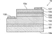
如图2所示,半导体发光元件10包括层叠的结构体,该层叠的结构体包括依次层叠在衬底90上的缓冲层101、n型接触层102、发光层103、p型电子阻挡层104、以及p型接触层105。缓冲层101可以包括,例如,多晶GaN;n型接触层102可以包括,例如,掺杂有Si的GaN。发光层103可以具有,例如,量子阱结构,在该量子阱结构中,多重地交替层叠势垒层和阱层。势垒层可以包括,例如,GaN;阱层可以包括,例如,InGaN。p型电子阻挡层104可以包括,例如,掺杂有Mg的AlGaN。p型接触层105可以包括,例如,掺杂有Mg的GaN。As shown in FIG. 2 , the semiconductor light-emitting
在该具体实例的半导体发光元件10的层叠结构体中,去除n型接触层102的一部分、以及发光层103、p型电子阻挡层104和p型接触层105的一部分;暴露n型接触层102的一部分。还将n侧电极108设置为连接到n型接触层102;并且还将p侧电极107设置为连接到p型接触层105。换言之,p侧电极107被设置在半导体发光元件10的位于p型半导体层(p型接触层105)侧的第一主表面10a上且与p型半导体层(p型接触层105)接触。半导体发光元件10的位于n型半导体层(n型接触层102)侧的第二主表面10b是与安装构件20相对的一侧的面。In the stacked structure of the semiconductor light-emitting
半导体发光元件10的每一个半导体层都可包括氮化物半导体。换言之,半导体发光元件10可包括,例如,蓝光发光二极管(LED)、蓝紫光LED、紫光LED、紫外光LED等等。然而,本发明的实施例不限于此。可以使用任何半导体发光元件10。Each semiconductor layer of the semiconductor
在如图1所示的该具体实例中,在安装构件20上设置p侧基底电极107e和n侧基底电极108e。p侧基底电极107e和n侧基底电极108e分别通过p侧互连107w和n侧互连108w而连接到半导体发光元件10的p侧电极107和n侧电极108。然而,上述描述是一个实例;本发明的实施例不限于此。可以对电连接的形式以及半导体发光元件10和安装构件20的配置进行各种修改。In this specific example shown in FIG. 1 , a p-
虽然在该具体实例中安装构件20是具有在其上安装半导体发光元件10的杯状结构的构件,但只要该安装构件20是可以在其上安装半导体发光元件10的部件就足够了。安装构件20的结构是任意的。安装构件20可以包括任何材料,例如,无机材料、有机材料等等。Although the mounting
安装构件20的在半导体发光元件10侧(第一波长转换层30侧)的面可以是具有高反射率的面。例如,可以在安装构件20的在半导体发光元件10侧的面上,即,安装构件20的安装面(在其上安装半导体发光元件10的面)上,设置由Ag等等构成的反射膜(未示出)。The surface of the mounting
第一波长转换层30可以包括分散在第一树脂32中的第一波长转换颗粒31,其中第一波长转换颗粒31吸收第一光并发射第二光。The first
第一波长转换颗粒31可以包括,例如,荧光剂细颗粒、氮化物半导体细颗粒等等。氮化物半导体可以包括AlxGayIn1-x-yN(0≤x≤1,0≤y≤1,且x+y≤1)。对于这样的氮化物半导体,可以通过改变上述x和y的值来改变所发射的波长。在上述氮化物半导体中,可以用B、Tl等等替代III族元素中的一部分。可以用P、As、Sb、Bi等等替代N的一部分。The first
第一波长转换颗粒31不限于一种类型的材料,可以包括两种或更多种类型的材料。The first
例如,可以使用基于硅氧烷(silicone)的树脂等等作为第一波长转换层30的第一树脂32。For example, a silicone-based resin or the like may be used as the
第一波长转换层30可以具有将半导体发光元件10接合到安装构件20的接合功能。换言之,可以使用具有接合功能的材料作为第一树脂32。从而,可以将半导体发光元件10固定到安装构件20而不设置单独的接合剂;可以抑制由单独地设置接合剂引起的发光效能的降低;并且可以简化工艺。The first
第二波长转换层80可以包括分散在第二树脂(未示出)中的第二波长转换颗粒(未示出),其中第二波长转换颗粒吸收第一光并发射第三光。The second
第二波长转换颗粒不限于一种类型的材料,可以包括两种或更多种类型的材料。The second wavelength converting particles are not limited to one type of material, but may include two or more types of materials.
第二波长转换颗粒可以包括,例如,荧光剂细颗粒、氮化物半导体细颗粒等等。例如,可以使用基于硅氧烷的树脂等等作为第二波长转换层80的第二树脂。The second wavelength conversion particles may include, for example, phosphor fine particles, nitride semiconductor fine particles, and the like. For example, a silicone-based resin or the like may be used as the second resin of the second
可以基于由半导体发光元件10发射的第一光的发光特性(例如,发光波长)和由第一波长转换层30发射的第二光的发光特性(例如,发光波长)来适当地设定由第二波长转换层80发射的第三光的发光特性(例如,发光波长)。The light emission characteristic (for example, light emission wavelength) of the first light emitted by the semiconductor
第三光的波长不大于第二光的波长。例如,在第一光是蓝光的情况下,第二光可以是黄光且第三光可以是黄光。并且,例如,在第一光是蓝光的情况下,第二光可以是红光且第三光可以是绿光。在例如第一光是近紫外光的情况下,第二光可以是黄光且第三光可以是蓝和绿光。The wavelength of the third light is not greater than the wavelength of the second light. For example, in case the first light is blue light, the second light may be yellow light and the third light may be yellow light. And, for example, in case the first light is blue light, the second light may be red light and the third light may be green light. In case eg the first light is near ultraviolet light, the second light may be yellow light and the third light may be blue and green light.
第一透明层60可以包括对第一光、第二光和第三光透明的任何材料。换言之,第一透明层对在半导体发光元件10的发光波长附近的波长以及比该波长更长的波长区域中的波长基本上透明。第一透明层60可包括,例如,诸如基于硅氧烷的树脂的任何有机材料等等。The first
例如,透明树脂层可以被设置为第一透明层60,例如,其外表面具有向上(沿着从安装构件20朝向半导体发光元件10的方向)凸起的弯曲结构以覆盖半导体发光元件10。具有向上突起结构的弯曲表面的截面的曲线可以具有任何结构,例如,半圆弧状结构、抛物线结构等等。For example, a transparent resin layer may be provided as the first
在该具体实例中,第一透明层60的端部接触安装构件20。由此,通过将第一透明层60设置为覆盖半导体发光元件10,第一透明层60可以保护半导体发光元件10;并且发光器件210的可靠性提高。然而,本发明的实施例不限于此。在一些情况下,第一透明层60的至少部分端部可以被设置为从安装构件20分离。In this particular example, the end of the first
图3是示例出根据本发明的第一实施例的发光器件的操作的示意图。Fig. 3 is a schematic diagram illustrating the operation of the light emitting device according to the first embodiment of the present invention.
如图3所示,由半导体发光元件10的发光层103发射的第一光L1的一部分朝向p型半导体层侧的第一主表面10a(上面)传播,穿过第一透明层60和第二波长转换层80,并被提取到发光器件210的外部。As shown in FIG. 3, a part of the first light L1 emitted by the
当朝向第一主表面10a传播的第一光L1穿过第一透明层60且进入第二波长转换层80时,在第二波长转换层80中吸收第一光L1的一部分;发射具有大于第一光L1的波长的波长特性的第三光L3;并且第三光L3被发射到发光器件210的外部。When the first light L1 propagating toward the first
此时,虽然在第二波长转换层80发射第三光L3时在第二波长转换层80中产生热,但第一透明层60被设置为覆盖半导体发光元件10;而且第二波长转换层80被设置在第一透明层60上。因此,即使在通过第二波长转换层80产生热的情况下,也可以抑制在第二波长转换层80与半导体发光元件10之间的热传导;可以抑制半导体发光元件10的温度的升高;并且可以保持半导体发光元件10的发光效能的高值。At this time, although heat is generated in the second
第一光L1的另一部分朝向n型半导体层(n型接触层102)侧的第二主表面10b(下面)传播,并进入第一波长转换层30。在第一波长转换层30中吸收第一光L1;并且发射具有大于第一光L1的波长的波长特性的第二光L2。The other part of the first light L1 propagates toward the second
在未设置第一波长转换层30的情况下,由于从半导体发光元件10发射到安装构件20侧的第一光L1被安装构件20反射、返回到半导体发光元件10的内部且被不希望地再吸收(特别地,被半导体发光元件10的发光层103再吸收),效率降低。In the case where the first
相反地,通过设置第一波长转换层30,从半导体发光元件10发射到安装构件20侧的第一光L1被转换成具有大于第一光L1的波长的第二光L2。从而,即使在第二光L2被安装构件20反射、返回到半导体发光元件10的内部且进入半导体发光元件10(特别地,进入发光层103)的情况下,由于第二光L2的波长大于第一光L1的波长,半导体发光元件10(特别地,发光层103)也不会容易地再吸收第二光L2。因此,第二光L2容易地从半导体发光元件10发射到外部;从而损耗低。Conversely, by providing the first
当第一波长转换层30发射第二光L2时,在第一波长转换层30中也产生热。此时,第一波长转换层30接触安装构件20。因此,第一波长转换层30的热被高效地传导到安装构件20并被散逸。因此,可以抑制由第一波长转换层30的发热引起的半导体发光元件10的温度的升高;并且可以保持半导体发光元件10的发光效能的高值。When the first
在发光器件210中,第一波长转换层30被设置在半导体发光元件10的第二主表面10b侧;并且第二波长转换层80被设置在第一主表面10a侧。从而,第一波长转换层30在第二波长转换层80的远侧。因此,例如,抑制了由第二波长转换层80发射的第三光L3进入第一波长转换层30且被再吸收。从而,发光效能也提高。In the
由此,根据发光器件210,可以提供具有高发光效能的发光器件。Thus, according to the
将第三光L3的波长设置为不大于第二光L2的波长可提高发光效能。换言之,在第二光L2的波长小于第三光L3的波长的情况下,当第二光L2穿过第二波长转换层80时,第二光L2被第二波长转换层80吸收;因而效率会降低。然而,通过将第三光L3的波长设置为不大于第二光L2的波长,抑制了在第二波长转换层80中对第二光L2的吸收;从而效率提高。Setting the wavelength of the third light L3 to be not greater than the wavelength of the second light L2 can improve the luminous efficacy. In other words, when the wavelength of the second light L2 is smaller than the wavelength of the third light L3, when the second light L2 passes through the second
第一比较例first comparative example
图4是示例出第一比较例的发光器件的结构的示意性截面图。4 is a schematic cross-sectional view illustrating the structure of a light emitting device of a first comparative example.
在如图4所示的第一比较例的发光器件219a中,未设置第一透明层60;直接在半导体发光元件10上设置第二波长转换层80。在安装构件20上设置基于硅氧烷的透明管芯接合材料层41(管芯接合粘合剂);在透明管芯接合材料层41上设置第一波长转换层30;此外在第一波长转换层30上设置半导体发光元件10。该结构对应于在JP-A 2001-210874(特开)中公开的结构。In the
在第一比较例的发光器件219a中,因为直接在半导体发光元件10上设置第二波长转换层80,由第二波长转换层80产生的热导致半导体发光元件10的温度升高。此外,因为在第一波长转换层30与安装构件20之间设置有基于硅氧烷的透明管芯接合材料层41,由第二波长转换层80产生的热不容易被传导到安装构件20且不容易被散逸;这也使得半导体发光元件10的温度升高。由此,在第一比较例的发光器件219a中,半导体发光元件10的温度升高;因此发光效能降低。In the
第二比较例Second comparative example
图5是示例出第二比较例的发光器件的结构的示意性截面图。Fig. 5 is a schematic cross-sectional view illustrating the structure of a light emitting device of a second comparative example.
在如图5所示的第二比较例的发光器件219a中,在根据该实施例的发光器件210的安装构件20与第一波长转换层30之间设置基于硅氧烷的透明管芯接合材料层41。In the
虽然在第二比较例的发光器件219b的半导体发光元件10上设置了第一透明层60以减轻由第二波长转换层80产生的热的影响,但在第一波长转换层30与安装构件20之间设置有基于硅氧烷的透明管芯接合材料层41。因此,由第二波长转换层80产生的热不能通过安装构件20容易地散逸;并且,如所预期的,半导体发光元件10的温度升高。因此,在第二比较例的发光器件219b中,同样地,半导体发光元件10的温度升高;因为发光效能降低。Although the first
第三比较例The third comparative example
图6是示例出第三比较例的发光器件的结构的示意性截面图。Fig. 6 is a schematic cross-sectional view illustrating the structure of a light emitting device of a third comparative example.
如图6所示,在第三比较例的发光器件219c中未设置第一波长转换层30。通过基于硅氧烷的透明管芯接合材料层41将半导体发光元件10接合到安装构件20。在第一透明层60上设置第二波长转换层80c。As shown in FIG. 6, the first
在第三比较例的发光器件219c中,在第二发光元件10上设置了第一透明层60。因此,由第二波长转换层80产生的热的影响降低。然而,由于未设置第一波长转换层30,从半导体发光元件10发射到安装构件20侧的第一光L1被安装构件20反射,返回到半导体发光元件10的内部,并被再吸收(特别地,被半导体发光元件10的发光层103再吸收);并且效率降低。In the
第四比较例Fourth comparative example
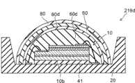
图7是示例出第四比较例的发光器件的结构的示意性截面图。7 is a schematic cross-sectional view illustrating the structure of a light emitting device of a fourth comparative example.
在如图7所示的第四比较例的发光器件219d中,未设置第一波长转换层30,同时,在半导体发光元件10与安装构件20之间设置了基于硅氧烷的透明管芯接合材料层41。还设置了第一透明层60和第二波长转换层80。在第一透明层60的内侧设置内波长转换层80d;并且在内波长转换层80d与半导体发光元件10之间设置内透明层60d。In the
在具有该结构的发光器件219d中,接近第二波长转换层80地设置内波长转换层80d。因此,由第二波长转换层80发射的第三光L3容易被内波长转换层80d吸收。虽然因为内波长转换层80d被来自半导体发光元件10的第一光L1直接激发而在内波长转换层80d中高效发光,但外侧的第二波长转换层80会被来自半导体发光元件10的第一光L1直接激发且会被内波长转换层80d反射或散射的第一光L1激发。因此,第二波长转换层80的发光效率降低,降低的量为由于被内波长转换层80d反射或散射而发生的损耗的量。因此,发光效能降低。In the
此外,在发光器件219d的情况下,未设置第一波长转换层30。因此,从半导体发光元件10朝向安装构件20发射的第一光L1被安装构件20反射,再次进入半导体发光元件10,并且由于再吸收(特别地,被半导体发光元件10的发光层103再吸收)而被损耗;因而发光效能降低。Furthermore, in the case of the
相反地,因为第一波长转换层30将第一光L1转换成具有大于第一光L1的波长的第二光L2,发光器件210可以抑制由于被安装构件20反射的光返回到半导体发光元件10的内部且被半导体发光元件10的发光层103再吸收而导致的效率降低。此外,因为第一波长转换层30接触安装构件20,散热性良好;并且,可以抑制由热引起的效率降低。Conversely, since the first
此外,通过在第二波长转换层80与半导体发光元件10之间设置第一透明层60,可以抑制由在第二波长转换层80的波长转换期间的发热引起的半导体发光元件10的温度升高;并且,可以抑制由半导体发光元件10的温度升高引起的发光效能的降低。通过将第一波长转换层30设置在半导体发光元件10的下侧且将第二波长转换层80设置在上侧,第一波长转换层30和第二波长转换层80在彼此的远侧。因此,例如,可以抑制由第二波长转换层80发射的第三光L3进入第一波长转换层30而被再吸收。从而,发光效能提高。Furthermore, by disposing the first
而且,通过在第二波长转换层80与半导体发光元件10之间设置第一透明层60,可以容易地调整第二波长转换层80的膜厚度;并且可以通过最优地调整膜厚度来抑制在第二波长转换层80中对第二光L2的再吸收。从而,可以获得具有高发光效能的发光器件。Moreover, by providing the first
例如,可以将第二波长转换层80的端部设置为接触安装构件20。从而,由第二波长转换层80产生的热可以被高效地传导到安装构件20;可以进一步降低半导体发光元件10的温度升高;可以提高半导体发光元件10的发光效能;从而可以进一步提高发光器件210的效率。For example, an end portion of the second
然而,本发明的实施例不限于此。在第二波长转换层80几乎不产生热的情况下、在半导体发光元件10的温度不会容易地升高的情况下、在即使半导体发光元件10的温度升高时发光效能也不会容易地降低的情况下,可以将第二波长转换层80的至少部分端部设置为从安装构件20分离。However, embodiments of the present invention are not limited thereto. In the case where the second
第一透明层60可以包括包含气体(包括空气)的层。从而,由第二波长转换层80产生的热不会被容易地传导到半导体发光元件10;从而效率提高。在第一透明层60为例如气体(包括空气)层的情况下,可以使用模具(die)形成第二波长转换层80,以使第二波长转换层80保持其自身的形状;并且所形成的第二波长转换层80可被设置在半导体发光元件10上以覆盖半导体发光元件10。The first
通过多重地设置波长转换层(例如第一波长转换层30和第二波长转换层80),更易于控制由发光器件210发射的光的波长特性;并且更易于实现具有高色彩再现性的希望的光发射。It is easier to control the wavelength characteristics of the light emitted by the
如上所述,在根据该实施例的发光器件210中,希望第三光L3的波长带不大于第二光L2的波长带。例如,第三光L3的波长带的最小波长不大于第二光L2的波长带的最小波长。例如,第三光L3的波长带的最大波长不大于第二光L2的波长带的最大波长。例如,第三光L3的波长带的最大波长可以等于或小于第二光L2的波长带的最小波长。As described above, in the
例如,在从半导体发光元件10发射的第一光L1为具有蓝色区中的发光峰的光的情况下,第一波长转换层30发射黄色的第二光L2(例如,荧光);并且第二波长转换层80也发射黄色的第三光L3。从而,发光器件210可以发射白光。For example, in the case where the first light L1 emitted from the semiconductor
此外,在从半导体发光元件10发射的第一光L1为具有蓝色区中的发光峰的光的情况下,第一波长转换层30发射红色的第二光L2(例如,荧光);并且第二波长转换层80发射绿色的第三光L3。从而,发光器件210发射红色、绿色和蓝色三种颜色的光,从而可以发射白光。Furthermore, in the case where the first light L1 emitted from the semiconductor
在从半导体发光元件10发射的第一光L1为具有近紫外区中的发光峰的光的情况下,第一波长转换层30可发射红色的第二光L2(例如,荧光);并且第二波长转换层80可发射绿色和蓝色的第三光L3。从而,发光器件210发射红色、绿色和蓝色三种颜色的光,从而可以发射白光。In the case where the first light L1 emitted from the semiconductor
由此,例如,可以使用黄光荧光剂作为第一波长转换层30的第一波长转换颗粒31;并且可以在第二波长转换层80中也使用黄光荧光剂。此外,例如,可以使用红光荧光剂作为第一波长转换层30的第一波长转换颗粒31;并且可以使用绿光荧光剂作为第二波长转换层80中的第二波长转换颗粒。此外,可以使用红光荧光剂作为第一波长转换层30的第一波长转换颗粒31;并且可以使用蓝光荧光剂和绿光荧光剂的两种类型荧光剂作为第二波长转换层80中的第二波长转换颗粒。Thus, for example, a yellow phosphor may be used as the first
然而,以上描述是在发光元件210发射白光的情况下的结构的实例。第一光L1、第二光L2和第三光L3的发光特性的组合是任意的。可以基于发光器件所要发射的光的规格来适当地设定第一光L1、第二光L2和第三光L3的发光特性。However, the above description is an example of the structure in the case where the
例如,在该实施例中,可以在第一波长转换层30和第二波长转换层80中使用红光荧光剂层、黄光荧光剂层、绿光荧光剂层和蓝光荧光剂层中的任何荧光剂层。For example, in this embodiment, any of a red phosphor layer, a yellow phosphor layer, a green phosphor layer, and a blue phosphor layer may be used in the first
红光荧光剂层可以发射例如600nm到780nm的波长范围内的光。黄光荧光剂层可以发射例如550nm到590nm的波长范围内的光。绿光荧光剂层可以发射例如475nm到520nm的波长范围内的光。蓝光荧光剂层可以发射例如430nm到475nm的波长范围内的光。The red phosphor layer may emit light in a wavelength range of, for example, 600nm to 780nm. The yellow phosphor layer may emit light in a wavelength range of, for example, 550 nm to 590 nm. The green phosphor layer may emit light in a wavelength range of, for example, 475nm to 520nm. The blue phosphor layer may emit light in a wavelength range of, for example, 430nm to 475nm.
红光荧光剂层可以包含,例如,CaAlSiN3:Eu的基于氮化物的荧光剂、或者基于赛隆(sialon)的荧光剂。特别地,在使用基于赛隆的荧光剂的情况下,优选使用The red phosphor layer may include, for example, a CaAlSiN3 :Eu nitride-based phosphor, or a sialon-based phosphor. In particular, in the case of using a sialon-based fluorescent agent, it is preferable to use
(M1-x,Rx)a1AlSib1Oc1Nd1组合物化学式(1)(M1-x , Rx )a1 AlSib1 Oc1 Nd1 composition chemical formula (1)
其中M为除了Si和Al的金属元素中的至少一种,特别地希望M为选自Ca和Sr的至少一种;R为发光中心元素,特别地希望R为Eu;并且x、a1、b1、c1和d1满足以下关系:0<x≤1,0.6<a1<0.95,2<b1<3.9,0.25<c1<0.45,以及4<d1<5.7。Wherein M is at least one of metal elements other than Si and Al, and it is particularly desirable that M is at least one selected from Ca and Sr; R is a luminescence center element, and it is particularly desirable that R is Eu; and x, a1, b1 , c1 and d1 satisfy the following relationships: 0<x≤1, 0.6<a1<0.95, 2<b1<3.9, 0.25<c1<0.45, and 4<d1<5.7.
通过使用组合物化学式(1)的基于赛隆的荧光剂,可以改善波长转换效率的温度特性;并且可以进一步提高在大电流密度区域中的效率。By using the sialon-based fluorescent agent of the composition chemical formula (1), temperature characteristics of wavelength conversion efficiency can be improved; and efficiency in a large current density region can be further improved.
黄光荧光剂层可以包含,例如,(Sr,Ca,Ba)2SiO4:Eu的基于硅酸盐的荧光剂。The yellow phosphor layer may comprise, for example, a silicate-based phosphor of (Sr, Ca, Ba)2 SiO4 :Eu.
绿光荧光剂层可以包含,例如,(Ba,Ca,Mg)10(PO4)6·Cl2:Eu的基于含卤磷酸盐(halophosphate)的荧光剂或者基于赛隆的荧光剂。特别地,在使用基于赛隆的荧光剂的情况下,优选使用The green phosphor layer may comprise, for example, a halophosphate-based phosphor of (Ba, Ca, Mg)10 (PO4 )6 ·Cl2 :Eu or a sialon-based phosphor. In particular, in the case of using a sialon-based fluorescent agent, it is preferable to use
(M1-x,Rx)a2AlSib2Oc2Nd2组合物化学式(2)(M1-x , Rx )a2 AlSib2 Oc2 Nd2 composition chemical formula (2)
其中M为除了Si和Al的金属元素中的至少一种,特别地希望M为选自Ca和Sr的至少一种;R为发光中心元素,特别地希望R为Eu;并且x、a2、b2、c2和d2满足以下关系:0<x≤1,0.93<a2<1.3,4.0<b2<5.8,0.6<c2<1,以及6<d2<11。通过使用组合物化学式(2)的基于赛隆的荧光剂,可以改善波长转换效率的温度特性;并且可以进一步提高在大电流密度区域中的效率。Wherein M is at least one of metal elements other than Si and Al, and it is particularly desirable that M is at least one selected from Ca and Sr; R is a luminescence center element, and it is particularly desirable that R is Eu; and x, a2, b2 , c2 and d2 satisfy the following relationships: 0<x≤1, 0.93<a2<1.3, 4.0<b2<5.8, 0.6<c2<1, and 6<d2<11. By using the sialon-based fluorescent agent of the composition chemical formula (2), temperature characteristics of wavelength conversion efficiency can be improved; and efficiency in a large current density region can be further improved.
蓝光荧光剂可以包含,例如,BaMgAl10O17:Eu的基于氧化物的荧光剂。The blue phosphor may comprise, for example, an oxide-based phosphor of BaMgAl10 O17 :Eu.
作为在第一波长转换层30和第二波长转换层80中使用的树脂(第一树脂32和第二树脂),可以使用任何树脂,而不论其类型如何,只要该树脂对在由半导体发光元件10发射的第一光L1的发光波长附近的波长以及大于该波长的波长区域中的波长基本透明即可。这样的树脂包括,例如,硅氧烷树脂、环氧树脂、具有环氧基团的聚二甲基硅氧烷衍生物、氧杂环丁烷(oxetane)树脂、丙烯酸树脂、环烯烃(cycloolefin)树脂、尿素树脂、碳氟化合物树脂、聚酰亚胺树脂等等。As the resins (the
第二波长转换层80可以具有这样的结构,其中层叠具有不同发光波长的多个荧光剂层。在该情况下,优选将多个荧光剂层层叠为使得具有较大波长的荧光剂层设置为比具有较小波长的荧光剂层更加朝向半导体发光元件10侧。The second
优选在第二波长转换层80的外侧(与半导体发光元件10相反的一侧)进一步设置另一个透明层。通过设置另一个透明层,被提取到外部的光的比例增大;并且效率进一步提高。换言之,抑制了由荧光剂颗粒的凹陷和凸起引起的在第二波长转换层80与外部介质(例如,空气)之间的界面处发生的反射和散射;降低了第二波长转换层80的再吸收;增大了被提取到外部的光的比例;从而提高效率。此外,通过设置另一透明层,可以提高可靠性。It is preferable to further provide another transparent layer on the outside of the second wavelength conversion layer 80 (the side opposite to the semiconductor light emitting element 10 ). By providing another transparent layer, the proportion of light extracted to the outside is increased; and the efficiency is further improved. In other words, the reflection and scattering that occur at the interface between the second
该另一个透明层可以由具有不同折射率的多个层形成。在该情况下,优选将这些层层叠为使其折射率从第二波长转换层80侧朝向外侧降低。由此,抑制了在第二波长转换层80与外部介质(例如,空气)之间的界面处的反射和散射;从而提高效率。This further transparent layer may be formed of layers having different refractive indices. In this case, it is preferable to stack these layers such that the refractive index decreases from the second
希望第一波长转换颗粒31的颗粒尺寸不小于1微米(μm)且不大于50μm。在第一波长转换颗粒31的颗粒尺寸不小于1μm且不大于50μm的情况下,第一波长转换层30的波长转换效率提高;从而发光效能提高。在第一波长转换颗粒31的颗粒尺寸小于1μm的情况下,第一光L1在第一波长转换层30中的吸收率降低;从而发光效能容易降低。在第一波长转换颗粒31的颗粒尺寸大于50μm的情况下,散热性差;从而发光效能会降低。在一些情况下,第一波长转换层30的接合强度会降低;从而发光器件的可靠性劣化。It is desirable that the particle size of the first
第一波长转换层30和第二波长转换层80中的至少一者可包括多个层。例如,第二波长转换层80可包括,例如,包含绿光荧光剂的绿光荧光剂层和层叠在绿光荧光剂层上的包含蓝光荧光剂的蓝光荧光剂层。第二波长转换层80可进一步包括设置在上述绿光荧光剂层与上述蓝光荧光剂层之间的另一透明层。从而,可以进一步改善光学特性和制造容易性二者。At least one of the first
第一实例first instance
下面将与比较例对比地描述根据该实施例的第一实例的发光器件的特性。第一实例的发光器件210a是这样的实例,其中从半导体发光元件10发射的第一光L1为蓝光,从第一波长转换层30和第二波长转换层80发射的光(第二光L2和第三光L3)都是黄光。The characteristics of the light emitting device according to the first example of this embodiment will be described below in comparison with a comparative example. The
第一实例的发光器件210a具有与图1所示的发光器件210的结构相似的结构。如下构造发光器件210a。The
使用由AlN制成的安装基底作为安装构件20。换言之,通过模制AlN材料来构造安装构件20。A mounting base made of AlN was used as the mounting
另一方面,作为半导体发光元件10,使用具有包含InGaN化合物半导体的发光层103的蓝光LED芯片。半导体发光元件10的发光波长(第一光L1的波长)的峰值为450nm。On the other hand, as the semiconductor
在安装构件20的安装面上形成第一波长转换层30。使用具有560nm的发光峰值的基于硅酸盐的黄光荧光剂(具有(Sr,Ca,Ba)2SiO4:Eu的组成)作为第一波长转换层30的第一波长转换颗粒31。使用基于硅氧烷的透明管芯接合材料作为第一树脂32。以50wt%(重量百分比)的浓度将具有约10μm的颗粒尺寸的第一波长转换颗粒31分散在第一树脂32中,然后将其涂覆到安装构件20的安装面上,从而形成第一波长转换层30。The first
通过将半导体发光元件10置于第一波长转换层30上并干燥第一波长转换层30,将半导体发光元件10接合到安装构件20并进行固定。随后,分别通过p侧互连107w和n侧互连108w而将安装构件20的p侧基底电极107e和n侧基底电极108e电连接到半导体发光元件10的p侧电极107和n侧电极108。By placing the semiconductor
然后,在半导体发光元件10上形成用于形成第一透明层60的硅氧烷树脂层。换言之,使用分配器涂覆硅氧烷树脂以覆盖半导体发光元件10,同时在大气压下在环境空气中将安装构件20加热到150℃的温度。硅氧烷树脂在顶部处的厚度与在端面处的厚度的比率基本上为1∶1,并且硅氧烷树脂被涂覆为向上突起的弯曲结构。然后,在大气压力下使硅氧烷树脂在150℃下干燥60分钟;从而形成第一透明层60。Then, a silicone resin layer for forming the first
另一方面,通过将基于硅酸盐的黄光荧光剂(具有(Sr,Ca,Ba)2SiO4:Eu的组成)分散在基于硅氧烷的透明树脂中,制备用于形成第二波长转换层80的黄光荧光剂分散树脂。使用分配器涂覆该黄光荧光剂分散树脂以覆盖整个第一透明层60,同时在环境空气中在大气压力下将安装构件20加热到150℃。黄光荧光剂分散树脂的膜厚度基本上均匀;并且该黄光荧光剂分散树脂具有向上突起的弯曲形状以与第一透明层60的结构相符。随后,在大气压力下使黄光荧光剂分散树脂在150℃下干燥60分钟;从而形成第二波长转换层80。第二波长转换层80在顶部处的厚度与在端面处的厚度的比率基本上为1∶1。On the other hand, by dispersing a silicate-based yellow fluorescent agent (having a composition of (Sr, Ca, Ba)2 SiO4 :Eu) in a siloxane-based transparent resin, for forming the second wavelength The yellow phosphor dispersion resin of the
由此,构造出第一实例的发光器件210a。Thus, the
测量发光器件210a的发光特性。当被20mA的电流驱动时,发光效能为84.9(lm/W);获得高效率。The light emitting characteristics of the
另一方面,构造出图5所示的第二比较例的发光器件219b。换言之,在安装构件20的安装面上设置基于硅氧烷的透明管芯接合材料层41;在基于硅氧烷的透明管芯接合材料层41上形成第一波长转换层30;并且在第一波长转换层30上设置半导体发光元件10。当被20mA的电流驱动时,具有该结构的发光器件219b的发光效能为83.8(lm/W);因此效率低于第一实例的发光器件210a的效率。On the other hand, the light emitting device 219b of the second comparative example shown in FIG. 5 was constructed. In other words, the silicone-based transparent die-
构造出图6所示的第三比较例的发光器件219c。换言之,在安装构件20的安装面上设置基于硅氧烷的透明管芯接合材料层41;在基于硅氧烷的透明管芯接合材料层41上设置半导体发光元件10;并且在进行电连接之后,形成第一透明层60和第二波长转换层80c。此时,将发光器件219c的第二波长转换层80c的规格调整为使得发光器件219c的发光颜色与第一实例的发光器件210a的发光颜色匹配。换言之,发光器件219c的第二波长转换层80c的厚度大于第一实例的发光器件210a的第二波长转换层80的厚度。当被20mA的电流驱动时,具有该结构的发光器件219c的发光效能为80.7(lm/W);因此效率低于第二比较例的效率。A
由此,根据该实施例,可以提供具有高发光效能的发光器件。Thus, according to this embodiment, a light emitting device having high luminous efficacy can be provided.
第一实例的发光器件210a、第二比较例的发光器件219b和第三比较例的发光器件219c的发光颜色的色度坐标为(0.34,0.35)。这些发光器件中的每一个的发光颜色为白光。根据第一实例的发光器件219a,提供了发射白光且具有高效率的发光器件。The chromaticity coordinates of the emission colors of the
由于在图4所示的第一比较例的发光器件219a中未设置第一透明层60,由第二波长转换层80产生的热使得半导体发光元件10的温度升高;因而半导体发光元件10的发光效能降低。此外,难以调整第二波长转换层80的膜厚度;第二波长转换层80中的再吸收增加;发光效能降低;并且发生发光波动和颜色不均匀。因此,这样的结构被认为具有比第二比较例更低的效率。Since the first
第二实施例second embodiment
图8是示例出根据本发明的第二实施例的发光器件的结构的示意性截面图。Fig. 8 is a schematic cross-sectional view illustrating the structure of a light emitting device according to a second embodiment of the present invention.
如图8所示,根据第二实施例的发光器件220还包括第二透明层40。第二透明层40被设置在半导体发光元件10与第一波长转换层30之间,且与半导体发光元件10和第一波长转换层30接触。第二透明层40对第一光L1和第二光L2透明。As shown in FIG. 8 , the light emitting device 220 according to the second embodiment further includes a second
第二透明层40可以包括对第一和第二光透明的任何材料。换言之,第二透明层40对半导体发光元件10的发光波长附近的波长以及大于该波长的波长区域中的波长基本上透明。第二透明层40可以包括,例如,诸如基于硅氧烷的树脂的任何有机材料以及任何无机材料,所述无机材料包括诸如SiO2的氧化物、诸如SiN的氮化物、以及诸如SiON的氧氮化物。The second
通过在根据本实施例的发光器件220中设置第二透明层40,被安装构件20反射的光被直接发射到外部而不返回到半导体发光元件10;从而进一步提高光提取效率。By providing the second
图9是示例出根据本发明的第二实施例的发光器件的操作的示意图。FIG. 9 is a schematic diagram illustrating the operation of the light emitting device according to the second embodiment of the present invention.
如图9所示,由第一波长转换层30发射的第二光L2在入射到半导体发光元件10之前进入第二透明层40。然后,第二波长传播通过第二透明层40且从第二透明层40的侧面提取到外部环境。As shown in FIG. 9 , the second light L2 emitted from the first
例如,通过被在第二透明层40与半导体发光元件10的第二透明层40侧的第二主表面10b之间的界面以及在第二透明层40与第一波长转换层30之间的界面反射、或者被在第二透明层40与第二主表面10b之间的界面以及在第一波长转换层30与安装构件20之间的界面反射,第二光L2传播通过第二透明层40。For example, through the interface between the second
从而,第二光L2基本上不进入半导体发光元件10的内部(特别地,不进入发光层103);因而抑制了由于在半导体发光元件10的内部(特别地,发光层103)中吸收第二光L2而引起的损耗。从而,效率进一步提高。Thereby, the second light L2 does not substantially enter the inside of the semiconductor light emitting element 10 (in particular, does not enter the light emitting layer 103); The loss caused by light L2. Thus, the efficiency is further improved.
从半导体发光元件10发射的第一光L1还可以传播通过第二透明层40,从而从第二透明层40的侧面提取到外部环境。The first light L1 emitted from the semiconductor
例如,通过被第二透明层40与半导体发光元件10的第二透明层40侧的第二主表面10b之间的界面以及在第二透明层40与第一波长转换层30之间的界面反射、或者被在第二透明层40与第二主表面10b之间的界面以及在第一波长转换层30与安装构件20之间的界面反射,第一光L1传播通过第二透明层40。For example, by being reflected by the interface between the second
从而,第一光L1基本上不从安装构件20侧进入半导体发光元件10的内部(特别地,不进入发光层103);因而抑制了由于在半导体发光元件10的内部(特别地,发光层103)中吸收第一光L1而引起的损耗。从而,效率进一步提高。Thereby, the first light L1 basically does not enter the inside of the semiconductor light emitting element 10 (particularly, the light emitting layer 103) from the side of the mounting
为了促进第一光L1和第二光L2传播通过第二透明层40,希望适当地设定第二透明层40、第一波长转换层30和半导体发光元件10(特别地,第二透明层40侧的部分)的折射率。In order to facilitate the propagation of the first light L1 and the second light L2 through the second
换言之,希望半导体发光元件10的接触第二透明层40的部分(即,第二主表面10b侧的部分,在该具体实例中,衬底90)的折射率(第一折射率n1)大于第二透明层40的折射率(第二折射率n2)。希望第一波长转换层30的接触第二透明层40的部分的折射率(第三折射率n3)不大于第二透明层40的折射率(第二折射率n2)。换言之,希望n3≤n2<n1。In other words, it is desirable that the portion of the semiconductor
通过将第一折射率n1设定为大于第二折射率n2,可以将从第二透明层40朝向半导体发光元件10传播的第二光L2高效地反射到第二透明层40侧。此外,可以使进入第二透明层40的第一光L1高效地传播通过第二透明层40。By setting the first refractive index n1 larger than the second refractive index n2, the second light L2 propagating from the second
通过将第三折射率n3设定为不大于第二折射率n2,第二光L2高效地从第一波长转换层30进入第二透明层40。此外,从第二透明层40朝向第一波长转换层30传播的第二光L2可以被在第二透明层40与第一波长转换层30之间的界面反射;并且第二光L2可以高效地传播通过第二透明层40。By setting the third refractive index n3 not greater than the second refractive index n2, the second light L2 efficiently enters the second
在第三折射率n3等于第二折射率n2的情况下,从第二透明层40朝向第一波长转换层30传播的第一光L1无损耗地穿过在第二透明层40与第一波长转换层30之间的界面;并且第一波长转换层30高效地发射第二光L2。此外,被安装构件20的在第一波长转换层30侧的面反射的第二光L2可以高效地进入第二透明层40;并且第二光L2可以高效地传播通过第二透明层40。此外,进入第二透明层40的第一光L1可以高效地传播通过第二透明层40。In the case where the third refractive index n3 is equal to the second refractive index n2, the first light L1 propagating from the second
例如,在该具体实例中,使用蓝宝石作为衬底90,其是半导体发光元件10的接触第二透明层40侧(第二主表面10b侧)的部分。在该情况下,第一折射率n1为约1.8。在半导体发光元件10的接触第二透明层40侧(第二主表面10b侧)的部分是n型接触层102(例如,GaN层)的情况下,第一折射率n1为约2.5。For example, in this specific example, sapphire is used as the
另一方面,可以使用例如基于硅氧烷的树脂作为第二透明层40;并且第二折射率n2可以为约1.5。第一波长转换层30可以包括分散在第一树脂32中的第一波长转换颗粒31;可以使用基于硅氧烷的树脂作为第一树脂32;并且第三折射率n3可为约1.4。由此,可以实现关系n3≤n2<n1。On the other hand, a silicone-based resin, for example, may be used as the second
通过将折射率设定为该关系,第一光L1和第二光L2被第二透明层40的半导体发光元件10侧的界面和第二透明层40的第一波长转换层30侧的界面高效地反射(即,经历全内反射)。从而,第一光L1和第二光L2可以高效地传播通过第二透明层40;该光可以被发射到外部而不进入半导体发光元件10;可以提高光提取效率;从而可以提高效率。By setting the refractive index to this relationship, the first light L1 and the second light L2 are efficiently transmitted by the interface of the second
由此,通过控制第一折射率n1、第二折射率n2和第三折射率n3之间的相互关系,进一步提高了效率。Thus, by controlling the relationship among the first refractive index n1, the second refractive index n2, and the third refractive index n3, the efficiency is further improved.
在发光器件220的情况下,同样地,第一波长转换层30接触安装构件20;并且由第一波长转换层30产生的热被安装构件20高效地传导并散逸。In the case of the light emitting device 220 , as well, the first
第二实例second instance
根据第二实施例的第二实例的发光器件220a具有与图8所示的发光器件220相似的结构。第二实例的发光器件220a是这样的实例,其中从半导体发光元件10发射的第一光L1是蓝光,并且从第一波长转换层30和第二波长转换层80发射的光(第二光L2和第三光L3)都是黄光。如下构造发光器件220a。A light emitting device 220a according to the second example of the second embodiment has a structure similar to that of the light emitting device 220 shown in FIG. 8 . The light emitting device 220a of the second example is an example in which the first light L1 emitted from the semiconductor
与第一实例相似地,使用由AlN制成的安装基底作为安装构件20。并且,作为半导体发光元件10,使用具有包含InGaN化合物半导体的发光层103的蓝光LED芯片(具有450nm的发光波长峰值)。Similar to the first example, a mounting base made of AlN was used as the mounting
首先,在半导体发光元件10的下面(第二主表面10b)上形成第二透明层40。使用透明硅氧烷树脂作为第二透明层40。换言之,通过在半导体发光元件10的下面(第二主表面10b)上涂覆硅氧烷树脂并在大气压力下使硅氧烷树脂在150℃下干燥10分钟到90分钟,获得第二透明层40。硅氧烷树脂的折射率(第二折射率n2)为1.54,其大于下述第一波长转换层30的1.41的折射率(第三折射率n3)且小于半导体发光元件10的衬底90的1.78的折射率(第一折射率n1)。First, the second
另一方面,与第一实例相似地,在安装构件20的安装面上形成第一波长转换层30。然后,将其上设置有第二透明层40的半导体发光元件10置于第一波长转换层30上;干燥第一波长转换层30;并且通过第一波长转换层30将半导体发光元件10接合到安装构件20并进行固定。On the other hand, the first
随后,与第一实例相似地,进行电连接;形成第一透明层60和第二波长转换层80。从而构造出第二实例的发光器件220a。Subsequently, similarly to the first example, electrical connection is made; the first
测量发光器件220a的发光特性。当被20mA的电流驱动时,发光效能为87.7(lm/W);效率比第一实例的发光器件210a的效率更高。The light emitting characteristics of the light emitting device 220a were measured. When driven by a current of 20 mA, the luminous efficacy is 87.7 (lm/W); the efficiency is higher than that of the
由此,根据该实施例,可以提供具有高发光效能的发光器件。Thus, according to this embodiment, a light emitting device having high luminous efficacy can be provided.
第二实例的发光器件220a的发光颜色的色度坐标为(0.34,0.35);因而发光器件220a的发光颜色为白光。The chromaticity coordinates of the light emitting color of the light emitting device 220a in the second example are (0.34, 0.35); thus the light emitting color of the light emitting device 220a is white light.
第三实例third example
根据第二实施例的第三实例的发光器件220b具有与图8所示的发光器件220相似的结构。然而,第三实例的发光器件220b是这样的实例,其中从半导体发光元件10发射的第一光L1为蓝光;从第一波长转换层30发射的第二光L2为红光;并且从第二波长转换层80发射的第三光L3为绿光。A light emitting device 220b according to the third example of the second embodiment has a structure similar to that of the light emitting device 220 shown in FIG. 8 . However, the light emitting device 220b of the third example is an example in which the first light L1 emitted from the semiconductor
如下构造发光器件220b。The light emitting device 220b is constructed as follows.
通过与第二实例相似的方法在半导体发光元件10的下面(第二主表面10b)上形成由硅氧烷树脂构成的第二透明层40。A second
另一反面,在安装构件20的安装面上形成第一波长转换层30。使用具有620nm的发光峰值的基于赛隆的红光荧光剂(具有Sr2Si7Al3ON13:Eu2+的组成)作为第一波长转换层30的第一波长转换颗粒31;并且使用基于硅氧烷的透明管芯接合材料作为第一树脂32。通过以50wt%(重量百分比)的浓度将第一波长转换颗粒31分散在第一树脂32中并在安装构件20的安装面上涂覆第一树脂32,形成第一波长转换层30。然后,通过与第一实例相似的方法,将半导体发光元件10接合到安装构件20并进行固定;并且,分别通过p侧互连107w和n侧互连108w而将p侧基底电极107e和n侧基底电极108e电连接到半导体发光元件10的p侧电极107和n侧电极108。On the other hand, the first
随后,在通过与第二实例相似的方法在半导体发光元件10上形成第一透明层60之后,在第一透明层60上形成绿光第二波长转换层80。换言之,通过将具有520nm的发光峰值的基于赛隆的绿光荧光剂(具有Sr3Si13Al3O2N21:Eu2+的组成)分散在基于硅氧烷的透明树脂中,制备用于形成第二波长转换层80的绿光荧光剂分散树脂。然后,通过与第二实例相似的方法涂覆该绿光荧光剂分散树脂以覆盖整个第一透明层60。绿光荧光剂分散树脂的膜厚度基本上均匀;并且该绿光荧光剂分散树脂的结构具有向上突起的弯曲结构以与第一透明层60的结构相符。随后,通过在大气压力下使绿光荧光剂分散树脂在150℃下干燥60分钟,形成第二波长转换层80。在该情况下,同样地,第二波长转换层80在顶部处的厚度与在端面处的厚度的比率基本上为1∶1。Subsequently, after the first
由此,构造出第三实例的发光器件220b。Thus, the light emitting device 220b of the third example was constructed.
另一方面,如下构造图7所示的第四比较例的发光器件219d。换言之,在使用基于硅氧烷的透明管芯接合材料层41将半导体发光元件10安装在安装构件20上之后进行电连接;并且通过使用与第一透明层60相似的方法形成内透明层60d。随后,通过使用与第二波长转换层80相似的方法将包含基于赛隆的红光荧光剂(具有Sr2Si7Al3ON13:Eu2+的组成)的红光荧光剂层形成为覆盖内透明层60d,形成内波长转换层80d。随后,通过与第三实例相似的方法,将第一透明层60形成为覆盖内波长转换层80d;并且通过将包含基于赛隆的绿光荧光剂(具有Sr3Si13Al3O2N21:Eu2+的组成)的绿光荧光剂层形成为覆盖第一透明层60而形成第二波长转换层80。由此,构造出发光器件219d。On the other hand, the
换言之,使用与第三实例的发光器件220b的第二透明层40相似的透明硅氧烷树脂作为第四比较例的发光器件219d的内透明层60d。使用与第三实例的发光器件220b的第一波长转换层30相似的材料作为第四比较例的发光器件219d的内波长转换层80d;并且内波长转换层80d是包含基于赛隆的红光荧光剂(具有Sr2Si7Al3ON13:Eu2+的组成)的红光荧光剂层。In other words, a transparent silicone resin similar to the second
使用与第三实例的发光器件220b的第一透明层60相似的材料作为第四比较例的发光器件219d的第一透明层60。使用与第三实例的发光器件220b的第二波长转换层80相似的包含基于赛隆的绿光荧光剂(具有Sr3Si13Al3O2N21:Eu2+的组成)的绿光荧光剂层作为第四比较例的发光器件219d的第二波长转换层80。As the first
评估诸如上述的第三实例的发光器件220b和第四比较例的发光器件219d的光学特性。The optical characteristics of the light emitting device 220b of the third example and the
发光器件220b和发光器件219d的发光颜色的色度坐标为(0.34,0.35);因而这两种发光器件都发射白光。The chromaticity coordinates of the emission colors of light emitting device 220b and light emitting
当被20mA的电流驱动时,第三实例的发光器件220b的发光效能为69.4(lm/W);获得高效率。When driven by a current of 20 mA, the light emitting efficacy of the light emitting device 220 b of the third example was 69.4 (lm/W); high efficiency was obtained.
另一方面,当被20mA的电流驱动时,第四比较例的发光器件219d的发光效能为60.1(lm/W);效率低。On the other hand, when driven by a current of 20 mA, the luminous efficacy of the
在第四比较例的发光器件219d的情况下,内波长转换层80d的红光荧光剂层被设置为接近第二波长转换层80的绿光荧光剂层。因此,作为由第二波长转换层80发射的绿光荧光的第三光L3容易在内波长转换层80d中被吸收。虽然内波长转换层80d被来自半导体发光元件10的第一光L1直接激发且可高效地发光,但外侧的第二波长转换层80被来自半导体发光元件10的第一光L1直接激发且被通过内波长转换层80d反射或散射的第一光L1激发。因此,第二波长转换层80的发光效率降低,降低量为由于被内波长转换层80d反射或散射而发生的损耗的量。从而,认为效率降低。此外,在发光器件219d的情况下,未设置第一波长转换层30。因此,从半导体发光元件10朝向安装构件20发射的第一光L1被安装构件20反射且再次进入半导体发光元件10;发生由于第一光L1被再吸收(特别地,被半导体发光元件10的发光层103再吸收)而导致的损耗;从而效率降低。In the case of the
另一方面,在其中设置了第二透明层40的第三实例的发光器件220b中,由红光第一波长转换层30发射的第二光L2(红光)没有进入半导体发光元件10的内部,而是传播通过第二透明层40,并且被直接提取到外部;抑制了由特别地半导体发光元件10的发光层103引起的再吸收损耗;抑制了由再吸收引起的发热;从而效率提高。On the other hand, in the light emitting device 220b of the third example in which the second
在第三实例的发光器件220b中,在半导体发光元件10与安装构件20之间设置了第一波长转换层30的红光荧光剂层;并且第一波长转换层30被设置在第二波长转换层80的绿光荧光剂层的远端。因此,由第二波长转换层80发射的绿色荧光的第三光L3基本上没有到达第一波长转换层30。从而,由第二波长转换层80发射的绿色第三光L3的大部分被发射到外部而未在第一波长转换层30和半导体发光元件10中被吸收;从而获得高效率。In the light emitting device 220b of the third example, the red phosphor layer of the first
由此,根据该实施例的发光器件220的形式可被应用于第三实例的发光器件220b,从而提供高效率地发射具有高色彩再现性的白光的发光器件。Thus, the form of the light emitting device 220 according to this embodiment may be applied to the light emitting device 220b of the third example, thereby providing a light emitting device that efficiently emits white light with high color reproducibility.
第三实施例third embodiment
图10A、图10B和图10C是示例出根据本发明的第三实施例的发光器件的结构的示意性截面图。10A, 10B and 10C are schematic cross-sectional views illustrating the structure of a light emitting device according to a third embodiment of the present invention.
在如图10A所示的根据该实施例的发光器件214中,去除了半导体发光元件10的衬底90(以及缓冲层101);半导体发光元件10的n型半导体层(n型接触层102)接触第二透明层40;并且在第二透明层40与安装构件20之间设置第一波长转换层30。由此,在根据本发明的实施例的发光器件中使用的半导体发光元件10具有包括设置在n型半导体层(即,n型接触层102)与p型半导体层(即,p型接触层105)之间的发光层103的结构就足够了,并且,必要时,可以省略例如衬底90等等。In the
在发光器件214中,同样地,通过设置第二波长转换层80、第一透明层60和第一波长转换层30,提高了效率。在该具体实例中,通过设置第二透明层40而进一步提高了效率。In the
可以从发光器件214的结构中省略第二透明层40。在该情况下,半导体发光元件10的n型半导体层(n型接触层102)接触第一波长转换层30。The second
在如图10B所示的根据该实施例的另一发光器件215中,将半导体发光元件10安装在安装构件20上,以使半导体发光元件10的p侧电极107和n侧电极108与安装构件20相对。换言之,半导体发光元件10的p型半导体层(p型接触层105)侧的第一主表面10a与安装构件20相对。通过p侧凸起107b将半导体发光元件10的p侧电极107电连接到安装构件20的p侧基底电极107e;并且通过n侧凸起108b将半导体发光元件10的n侧电极108电连接到安装构件20的n侧基底电极108e。In another light-emitting
在如图10C所示的根据该实施例的另一发光器件216中,去除了半导体发光元件10的衬底90(以及缓冲层101);并且将半导体发光元件10安装在安装构件20上,以使半导体发光元件10的p侧电极107和n侧电极108与安装构件20相对。In another
在发光器件215和216中,同样地,通过设置第二波长转换层80、第一透明层60和第一波长转换层30,提高了效率。在这些具体实例中,通过设置第二透明层40而进一步提高了效率。In the
在采用倒装芯片结构的发光器件215和216中提供的优点在于,由于不需要引线(p侧互连107w和n侧互连108w),可以提高发光器件的可靠性,并且不会发生由第一透明层60等等中的应力而发生的引线的断裂故障等等。The advantage provided in the light-emitting
可以从发光器件215和216的结构中省略第二透明层40。在该情况下,半导体发光元件10的p型半导体层(p型接触层105)和部分n型半导体层(n型接触层102)接触第一波长转换层30。在例如使用透明电极作为n侧电极108的情况下,可以使用其中n侧电极108接触第一波长转换层30的结构。The second
图11A和11B是示例出根据本发明的第三实施例的其他发光器件的结构的示意性截面图。11A and 11B are schematic cross-sectional views illustrating the structure of other light emitting devices according to the third embodiment of the present invention.
在如图11A所示的根据该实施例的发光器件218中,去除了半导体发光元件10的衬底90(以及缓冲层101);并且将n侧电极108设置在半导体发光元件10的n型半导体层(n型接触层102)侧的第二主表面10b上。例如,使用透明电极作为n侧电极108。将p侧电极107设置在p型半导体层(p型接触层105)侧的第一主表面10a上。通过n侧凸起108b将半导体发光元件10的n侧电极108电连接到安装构件20的n侧基底电极108e;并且通过p侧互连107w将半导体发光元件10的p侧电极107电连接到安装构件20的p侧基底电极107e。In the
在半导体发光元件10的与第一波长转换层30相反的一侧设置第二波长转换层80;在半导体发光元件10与第二波长转换层80之间设置第一透明层60;并且在半导体发光元件10的第二主表面10b侧设置第一波长转换层30。在该具体实例中,进一步设置第二透明层40。对于具有该结构的发光器件218,也提高了效率。A second
可以从该结构中省略第二透明层40。在该情况下,半导体发光元件10的n型半导体层(n型接触层102)接触第一波长转换层30。在例如使用透明电极作为n侧电极108的情况下,可以使用其中n侧电极108接触第一波长转换层30的结构。The second
在如图11B所示的根据该实施例的发光器件218a中,半导体发光元件10的衬底90是导电性的;衬底90接触第二透明层40;并且在第二透明层40与安装构件20之间设置第一波长转换层30。例如,使用SiC衬底作为衬底90。在衬底90侧的第二主表面10b上设置n侧电极108。在p型半导体层(p型接触层105)侧的第一主表面10a上设置p侧电极107。通过n侧凸起108b将半导体发光元件10的n侧电极108电连接到安装构件20的n侧基底电极108e;并且通过p侧互连107w将半导体发光元件10的p侧电极107电连接到安装构件20的p侧基底电极107e。In the
在该情况下,同样地,设置第二波长转换层80、第一透明层60和第一波长转换层30;并且进一步设置第二透明层40。对于具有该结构的发光器件218a,同样提高了效率。In this case, too, the second
可以从该结构中省略第二透明层40。在该情况下,半导体发光元件10的衬底90接触第一波长转换层30。在例如使用透明电极作为n侧电极108的情况下,可以使用其中n侧电极108接触第一波长转换层30的结构。The second
通过在发光器件218和218a中设置多个波长转换层(第一波长转换层30和第二波长转换层80),同样地,可以容易地控制由发光器件发射的光的发光特性;并且可以更容易地实现具有高色彩再现性的所希望的光发射。By arranging a plurality of wavelength conversion layers (the first
由此,在根据本发明的发光器件中,通过使用在半导体发光元件10的下面上设置的第一波长转换层30以进行对从半导体发光元件10发射到安装构件20侧的第一光L1的波长转换并产生具有大于半导体发光元件10的发光波长(第一光L1的波长)的波长的第二光L2,可以抑制由于被安装构件20反射的返回光被半导体发光元件10的发光层103再吸收而导致的损耗。通过接触安装构件20的第一波长转换层30而使散热性提高;抑制了半导体发光元件10的温度升高;从而提高了效率。Thus, in the light emitting device according to the present invention, the conversion of the first light L1 emitted from the semiconductor
通过在半导体发光元件10的上面上设置第一透明层60,抑制了第一波长转换层30对由第二波长转换层80发射的第三光L3的再吸收;从而提高了效率。此外,通过在半导体发光元件10与第二波长转换层80之间设置第一透明层60,第二波长转换层80与第一波长转换层30之间的距离增大,从而进一步抑制了上述再吸收;抑制了由第二波长转换层80产生的热引起的半导体发光元件10的温度升高;从而提高了效率。By disposing the first
通过在半导体发光元件10与第一波长转换层30之间设置第二透明层40,可以将被安装构件20反射的光(第一光L1和第二光L2)直接发射到外部而不穿过半导体发光元件10;因而提高了光提取效率。从而,可以提供具有高效率的发光器件。By providing the second
上文中,参考具体实例描述了本发明的示例性实施例。然而,本发明不限于这些具体实例。例如,通过从已知技术进行适当选择,本领域技术人员可以类似地实施本发明,包括由本领域技术人员进行的关于在发光器件中包括的部件(例如半导体发光元件、安装构件、第一波长转换层、第二波长转换层、第二透明层、第一透明层、半导体层、发光层、电极、互连等等)的具体结构的结构、尺寸、材料质量、排列等等的各种修改。这样的实施以与获得相似效果的程度而被包括在本发明的范围中。Hereinbefore, the exemplary embodiments of the present invention have been described with reference to specific examples. However, the present invention is not limited to these specific examples. For example, by appropriately selecting from known techniques, those skilled in the art can similarly implement the present invention, including the parts (such as semiconductor light emitting elements, mounting members, first wavelength conversion components, etc.) layer, second wavelength conversion layer, second transparent layer, first transparent layer, semiconductor layer, light-emitting layer, electrodes, interconnections, etc.) of various modifications of the structure, size, material quality, arrangement, etc. of the specific structure. Such implementation is included in the scope of the present invention to the extent similar effects are obtained.
此外,具体实例的任何两个或多个部件可以在技术可行性的范围内进行组合,且以包括本发明的主旨的程度而被包括在本发明的范围中。Furthermore, any two or more components of the specific examples may be combined within the range of technical feasibility, and are included in the scope of the present invention to the extent that the gist of the present invention is included.
而且,通过由本领域技术人员基于如以上本发明的实施例所述的发光器件进行的适当设计修改而可实施的所有发光器件也以包括本发明的主旨的程度而被包括在本发明的范围中。Also, all light-emitting devices that can be implemented by appropriate design modifications based on the light-emitting devices described in the embodiments of the present invention above by those skilled in the art are also included in the scope of the present invention to the extent that they include the gist of the present invention .
此外,在本发明的精神内的各种修改和改变对于本领域技术人员而言是显而易见的。因此,所有这样的修改和改变应被视为在本发明的范围内。Furthermore, various modifications and changes within the spirit of the invention will be apparent to those skilled in the art. Accordingly, all such modifications and changes should be considered within the scope of the present invention.
虽然已经描述了特定实施例,但这些实施例仅仅通过实例给出,并不旨在限制本发明的范围。实际上,在此描述的新颖实施例可以体现为各种其他形式;此外,可以在不脱离本发明的精神的情况下对在此描述的实施例的形式进行各种省略、替代和变化。所附权利要求及其等价物旨在涵盖落在本发明的范围和精神内的这些形式或修改。While specific embodiments have been described, these embodiments have been presented by way of example only, and are not intended to limit the scope of the inventions. Indeed, the novel embodiments described herein may be embodied in various other forms; furthermore, various omissions, substitutions and changes in the form of the embodiments described herein may be made without departing from the spirit of the inventions. The appended claims and their equivalents are intended to cover such forms or modifications as fall within the scope and spirit of the invention.
Claims (19)
Translated fromChineseApplications Claiming Priority (2)
| Application Number | Priority Date | Filing Date | Title |
|---|---|---|---|
| JP2009290554AJP5050045B2 (en) | 2009-12-22 | 2009-12-22 | Light emitting device |
| JP290554/2009 | 2009-12-22 |
Publications (2)
| Publication Number | Publication Date |
|---|---|
| CN102104107A CN102104107A (en) | 2011-06-22 |
| CN102104107Btrue CN102104107B (en) | 2013-09-25 |
Family
ID=43602855
Family Applications (1)
| Application Number | Title | Priority Date | Filing Date |
|---|---|---|---|
| CN2010102744342AExpired - Fee RelatedCN102104107B (en) | 2009-12-22 | 2010-09-07 | Light emitting device |
Country Status (6)
| Country | Link |
|---|---|
| US (2) | US8368104B2 (en) |
| EP (2) | EP3270426B1 (en) |
| JP (1) | JP5050045B2 (en) |
| KR (1) | KR101202110B1 (en) |
| CN (1) | CN102104107B (en) |
| TW (2) | TWI430480B (en) |
Families Citing this family (30)
| Publication number | Priority date | Publication date | Assignee | Title |
|---|---|---|---|---|
| JP5047264B2 (en) | 2009-12-22 | 2012-10-10 | 株式会社東芝 | Light emitting device |
| TW201238406A (en)* | 2011-03-11 | 2012-09-16 | Ind Tech Res Inst | Light emitting devices |
| US8952402B2 (en) | 2011-08-26 | 2015-02-10 | Micron Technology, Inc. | Solid-state radiation transducer devices having flip-chip mounted solid-state radiation transducers and associated systems and methods |
| CN103378274A (en)* | 2012-04-27 | 2013-10-30 | 台达电子工业股份有限公司 | Light emitting device and method for manufacturing the same |
| CN102709453B (en)* | 2012-05-30 | 2015-06-10 | 上舜照明(中国)有限公司 | LED (Light Emitting Diode) light source of double-layer fluorescent powder structure and manufacturing method |
| CN103545404B (en)* | 2012-07-09 | 2016-12-21 | 奇菱光电股份有限公司 | Quantum dot stack structure, manufacturing method thereof, and light-emitting element |
| WO2014053953A1 (en)* | 2012-10-04 | 2014-04-10 | Koninklijke Philips N.V. | Light emitting device |
| JP2014120514A (en)* | 2012-12-13 | 2014-06-30 | Sharp Corp | Semiconductor light-emitting device |
| JP2014139999A (en)* | 2013-01-21 | 2014-07-31 | Toshiba Corp | Semiconductor light-emitting device |
| US9484504B2 (en)* | 2013-05-14 | 2016-11-01 | Apple Inc. | Micro LED with wavelength conversion layer |
| TWI510741B (en)* | 2013-05-27 | 2015-12-01 | Genesis Photonics Inc | Illuminating device |
| TW201445082A (en)* | 2013-05-29 | 2014-12-01 | Genesis Photonics Inc | Illuminating device |
| US9111464B2 (en) | 2013-06-18 | 2015-08-18 | LuxVue Technology Corporation | LED display with wavelength conversion layer |
| US8928021B1 (en)* | 2013-06-18 | 2015-01-06 | LuxVue Technology Corporation | LED light pipe |
| TWI676300B (en)* | 2013-06-27 | 2019-11-01 | 晶元光電股份有限公司 | Light-emitting diode assembly |
| JP2015166416A (en)* | 2014-03-03 | 2015-09-24 | 株式会社東芝 | Phosphor, phosphor manufacturing method, and light emitting device using the same |
| CN103887406B (en)* | 2014-03-14 | 2016-06-15 | 苏州晶品光电科技有限公司 | Multi-level multimedium LED encapsulating structure |
| CN103915550B (en)* | 2014-03-14 | 2016-08-31 | 苏州晶品光电科技有限公司 | Light emitting semiconductor device based on fluorescent material |
| JP6217705B2 (en)* | 2015-07-28 | 2017-10-25 | 日亜化学工業株式会社 | Light emitting device and manufacturing method thereof |
| DE102016124526A1 (en)* | 2016-12-15 | 2018-06-21 | Osram Opto Semiconductors Gmbh | Component with an optoelectronic component |
| DE102017101729A1 (en)* | 2017-01-30 | 2018-08-02 | Osram Opto Semiconductors Gmbh | Radiation-emitting device |
| US10256376B1 (en)* | 2018-01-16 | 2019-04-09 | Leedarson Lighting Co. Ltd. | LED device |
| CN207834349U (en)* | 2018-01-16 | 2018-09-07 | 漳州立达信光电子科技有限公司 | A kind of LED packaging structure |
| US10243116B1 (en)* | 2018-01-16 | 2019-03-26 | Leedarson Lighting Co. Ltd. | LED device |
| US10069047B1 (en)* | 2018-01-16 | 2018-09-04 | Leedarson Lighting Co. Ltd. | LED device |
| TWI671558B (en)* | 2019-02-21 | 2019-09-11 | 友達光電股份有限公司 | Light emitting device and liquid crystal display device |
| KR20210115966A (en)* | 2020-03-17 | 2021-09-27 | 엘지이노텍 주식회사 | Lighting module and lighting device having thereof |
| WO2021205716A1 (en)* | 2020-04-09 | 2021-10-14 | シャープ株式会社 | Wavelength conversion element and optical device |
| KR20230019856A (en)* | 2020-06-03 | 2023-02-09 | 뷰리얼 인크. | Color Conversion Solid State Device |
| DE102021112359A1 (en) | 2021-05-12 | 2022-11-17 | OSRAM Opto Semiconductors Gesellschaft mit beschränkter Haftung | OPTOELECTRONIC LIGHTING DEVICE |
Citations (4)
| Publication number | Priority date | Publication date | Assignee | Title |
|---|---|---|---|---|
| CN1523683A (en)* | 2003-02-20 | 2004-08-25 | ������������ʽ���� | light emitting device |
| CN101124683A (en)* | 2004-12-24 | 2008-02-13 | 京瓷株式会社 | Light emitting device and lighting device |
| CN101176212A (en)* | 2005-03-14 | 2008-05-07 | 飞利浦拉米尔德斯照明设备有限责任公司 | Wavelength converted semiconductor light emitting device |
| CN101208811A (en)* | 2005-08-05 | 2008-06-25 | 松下电器产业株式会社 | semiconductor light emitting device |
Family Cites Families (13)
| Publication number | Priority date | Publication date | Assignee | Title |
|---|---|---|---|---|
| JPH10163527A (en)* | 1996-11-27 | 1998-06-19 | Matsushita Electron Corp | Surface light source |
| KR100425566B1 (en)* | 1999-06-23 | 2004-04-01 | 가부시키가이샤 시티즌 덴시 | Light emitting diode |
| JP3748355B2 (en) | 2000-01-27 | 2006-02-22 | シャープ株式会社 | Light emitting diode |
| JP2001223388A (en)* | 2000-02-09 | 2001-08-17 | Nippon Leiz Co Ltd | Light source device |
| KR101114305B1 (en) | 2004-12-24 | 2012-03-08 | 쿄세라 코포레이션 | Light-emitting device and illuminating device |
| US7514721B2 (en)* | 2005-11-29 | 2009-04-07 | Koninklijke Philips Electronics N.V. | Luminescent ceramic element for a light emitting device |
| JP2007273562A (en) | 2006-03-30 | 2007-10-18 | Toshiba Corp | Semiconductor light emitting device |
| US8502364B2 (en)* | 2006-08-22 | 2013-08-06 | Mitsubishi Chemical Corporation | Semiconductor device member, production method of semiconductor-device-member formation liquid and semiconductor device member, and semiconductor-device-member formation liquid, phosphor composition, semiconductor light-emitting device, lighting system and image display system using the same |
| JP4905009B2 (en)* | 2006-09-12 | 2012-03-28 | 豊田合成株式会社 | Method for manufacturing light emitting device |
| JP5044329B2 (en) | 2007-08-31 | 2012-10-10 | 株式会社東芝 | Light emitting device |
| JP2009141219A (en)* | 2007-12-07 | 2009-06-25 | Panasonic Electric Works Co Ltd | Light emitting device |
| JP5133120B2 (en)* | 2008-04-24 | 2013-01-30 | シチズン電子株式会社 | Light emitting device |
| JP2009267289A (en)* | 2008-04-30 | 2009-11-12 | Citizen Electronics Co Ltd | Light-emitting device |
- 2009
- 2009-12-22JPJP2009290554Apatent/JP5050045B2/ennot_activeExpired - Fee Related
- 2010
- 2010-09-02USUS12/874,413patent/US8368104B2/ennot_activeExpired - Fee Related
- 2010-09-03TWTW099129914Apatent/TWI430480B/ennot_activeIP Right Cessation
- 2010-09-03TWTW102148180Apatent/TW201419592A/enunknown
- 2010-09-06EPEP17188021.4Apatent/EP3270426B1/enactiveActive
- 2010-09-06EPEP10251556.6Apatent/EP2339656B1/ennot_activeNot-in-force
- 2010-09-07CNCN2010102744342Apatent/CN102104107B/ennot_activeExpired - Fee Related
- 2010-09-08KRKR1020100088043Apatent/KR101202110B1/ennot_activeExpired - Fee Related
- 2012
- 2012-11-15USUS13/677,828patent/US8592850B2/enactiveActive
Patent Citations (4)
| Publication number | Priority date | Publication date | Assignee | Title |
|---|---|---|---|---|
| CN1523683A (en)* | 2003-02-20 | 2004-08-25 | ������������ʽ���� | light emitting device |
| CN101124683A (en)* | 2004-12-24 | 2008-02-13 | 京瓷株式会社 | Light emitting device and lighting device |
| CN101176212A (en)* | 2005-03-14 | 2008-05-07 | 飞利浦拉米尔德斯照明设备有限责任公司 | Wavelength converted semiconductor light emitting device |
| CN101208811A (en)* | 2005-08-05 | 2008-06-25 | 松下电器产业株式会社 | semiconductor light emitting device |
Non-Patent Citations (1)
| Title |
|---|
| JP特开2009-267289A 2009.11.12 |
Also Published As
| Publication number | Publication date |
|---|---|
| US20130069098A1 (en) | 2013-03-21 |
| EP2339656A3 (en) | 2013-07-10 |
| JP5050045B2 (en) | 2012-10-17 |
| US8592850B2 (en) | 2013-11-26 |
| TWI430480B (en) | 2014-03-11 |
| KR101202110B1 (en) | 2012-11-15 |
| US8368104B2 (en) | 2013-02-05 |
| CN102104107A (en) | 2011-06-22 |
| EP3270426A1 (en) | 2018-01-17 |
| JP2011134762A (en) | 2011-07-07 |
| EP2339656A2 (en) | 2011-06-29 |
| TW201128815A (en) | 2011-08-16 |
| EP2339656B1 (en) | 2017-10-25 |
| KR20110073230A (en) | 2011-06-29 |
| US20110147775A1 (en) | 2011-06-23 |
| TW201419592A (en) | 2014-05-16 |
| EP3270426B1 (en) | 2019-12-18 |
Similar Documents
| Publication | Publication Date | Title |
|---|---|---|
| CN102104107B (en) | Light emitting device | |
| CN102104106B (en) | Light emitting device | |
| US8310145B2 (en) | Light emitting device including first and second red phosphors and a green phosphor | |
| US20110012141A1 (en) | Single-color wavelength-converted light emitting devices | |
| US8471277B2 (en) | Light emitting device | |
| CN103918093A (en) | Semiconductor light emitting device | |
| JP2009224538A (en) | Semiconductor light emitting device | |
| CN103779373A (en) | Light-emitting device and method of manufacturing the same | |
| JP4213168B2 (en) | Light emitting device | |
| CN102263191B (en) | Light emitting device package | |
| JP2015188050A (en) | light-emitting device | |
| JP5380588B2 (en) | Light emitting device | |
| JP5546589B2 (en) | Light emitting device | |
| CN104662681B (en) | Optoelectronic device comprising a transparent outcoupling element |
Legal Events
| Date | Code | Title | Description |
|---|---|---|---|
| C06 | Publication | ||
| PB01 | Publication | ||
| C10 | Entry into substantive examination | ||
| SE01 | Entry into force of request for substantive examination | ||
| C14 | Grant of patent or utility model | ||
| GR01 | Patent grant | ||
| TR01 | Transfer of patent right | Effective date of registration:20180109 Address after:Tokyo, Japan, Japan Patentee after:Alpha to KK Address before:Tokyo, Japan, Japan Patentee before:Toshiba Corp | |
| TR01 | Transfer of patent right | ||
| CF01 | Termination of patent right due to non-payment of annual fee | Granted publication date:20130925 Termination date:20200907 | |
| CF01 | Termination of patent right due to non-payment of annual fee |