CN102104062B - bipolar transistor - Google Patents
bipolar transistorDownload PDFInfo
- Publication number
- CN102104062B CN102104062BCN2009102020117ACN200910202011ACN102104062BCN 102104062 BCN102104062 BCN 102104062BCN 2009102020117 ACN2009102020117 ACN 2009102020117ACN 200910202011 ACN200910202011 ACN 200910202011ACN 102104062 BCN102104062 BCN 102104062B
- Authority
- CN
- China
- Prior art keywords
- region
- collector
- conductivity type
- pseudo
- bipolar transistor
- Prior art date
- Legal status (The legal status is an assumption and is not a legal conclusion. Google has not performed a legal analysis and makes no representation as to the accuracy of the status listed.)
- Active
Links
- 229910021420polycrystalline siliconInorganic materials0.000claimsabstractdescription14
- 150000002500ionsChemical class0.000claimsabstractdescription8
- 239000012535impuritySubstances0.000claimsdescription19
- 229920005591polysiliconPolymers0.000claimsdescription13
- 238000002513implantationMethods0.000claimsdescription12
- 229910052751metalInorganic materials0.000claimsdescription10
- 239000002184metalSubstances0.000claimsdescription10
- QVGXLLKOCUKJST-UHFFFAOYSA-Natomic oxygenChemical compound[O]QVGXLLKOCUKJST-UHFFFAOYSA-N0.000claimsdescription8
- 238000005468ion implantationMethods0.000claimsdescription8
- 229910052760oxygenInorganic materials0.000claimsdescription8
- 239000001301oxygenSubstances0.000claimsdescription8
- 239000010409thin filmSubstances0.000claimsdescription6
- 239000007943implantSubstances0.000claimsdescription5
- 229910052723transition metalInorganic materials0.000claimsdescription5
- 150000003624transition metalsChemical class0.000claimsdescription5
- 238000009792diffusion processMethods0.000claimsdescription4
- NMJKIRUDPFBRHW-UHFFFAOYSA-NtitaniumChemical compound[Ti].[Ti]NMJKIRUDPFBRHW-UHFFFAOYSA-N0.000claimsdescription4
- WFKWXMTUELFFGS-UHFFFAOYSA-NtungstenChemical compound[W]WFKWXMTUELFFGS-UHFFFAOYSA-N0.000claimsdescription4
- 229910052721tungstenInorganic materials0.000claimsdescription4
- 239000010937tungstenSubstances0.000claimsdescription4
- 238000000034methodMethods0.000abstractdescription11
- 230000003071parasitic effectEffects0.000abstractdescription7
- 238000002347injectionMethods0.000abstractdescription6
- 239000007924injectionSubstances0.000abstractdescription6
- 238000001259photo etchingMethods0.000abstractdescription2
- 230000005540biological transmissionEffects0.000abstract2
- 239000010410layerSubstances0.000description79
- 239000010408filmSubstances0.000description15
- VYPSYNLAJGMNEJ-UHFFFAOYSA-NSilicium dioxideChemical compoundO=[Si]=OVYPSYNLAJGMNEJ-UHFFFAOYSA-N0.000description13
- 229910052814silicon oxideInorganic materials0.000description13
- 238000010586diagramMethods0.000description8
- 238000002955isolationMethods0.000description6
- 238000000206photolithographyMethods0.000description6
- INQLNSVYIFCUML-QZTLEVGFSA-N[[(2r,3s,4r,5r)-5-(6-aminopurin-9-yl)-3,4-dihydroxyoxolan-2-yl]methoxy-hydroxyphosphoryl] [(2r,3s,4r,5r)-5-(4-carbamoyl-1,3-thiazol-2-yl)-3,4-dihydroxyoxolan-2-yl]methyl hydrogen phosphateChemical compoundNC(=O)C1=CSC([C@H]2[C@@H]([C@H](O)[C@@H](COP(O)(=O)OP(O)(=O)OC[C@@H]3[C@H]([C@@H](O)[C@@H](O3)N3C4=NC=NC(N)=C4N=C3)O)O2)O)=N1INQLNSVYIFCUML-QZTLEVGFSA-N0.000description5
- 238000004519manufacturing processMethods0.000description5
- 239000000758substrateSubstances0.000description5
- 229910052581Si3N4Inorganic materials0.000description4
- 230000015556catabolic processEffects0.000description4
- 238000000407epitaxyMethods0.000description4
- 239000004065semiconductorSubstances0.000description4
- XUIMIQQOPSSXEZ-UHFFFAOYSA-NSiliconChemical compound[Si]XUIMIQQOPSSXEZ-UHFFFAOYSA-N0.000description3
- 150000001875compoundsChemical class0.000description3
- 238000005516engineering processMethods0.000description3
- 238000005530etchingMethods0.000description3
- 238000011065in-situ storageMethods0.000description3
- 239000011229interlayerSubstances0.000description3
- 229910052710siliconInorganic materials0.000description3
- 239000010703siliconSubstances0.000description3
- HQVNEWCFYHHQES-UHFFFAOYSA-Nsilicon nitrideChemical compoundN12[Si]34N5[Si]62N3[Si]51N64HQVNEWCFYHHQES-UHFFFAOYSA-N0.000description3
- 229910000577Silicon-germaniumInorganic materials0.000description2
- 239000005380borophosphosilicate glassSubstances0.000description2
- 238000009826distributionMethods0.000description2
- 239000005360phosphosilicate glassSubstances0.000description2
- 238000005498polishingMethods0.000description2
- 239000000126substanceSubstances0.000description2
- 229910003811SiGeCInorganic materials0.000description1
- 230000003321amplificationEffects0.000description1
- 230000015572biosynthetic processEffects0.000description1
- 238000011982device technologyMethods0.000description1
- 238000011143downstream manufacturingMethods0.000description1
- 238000001312dry etchingMethods0.000description1
- BHEPBYXIRTUNPN-UHFFFAOYSA-Nhydridophosphorus(.) (triplet)Chemical compound[PH]BHEPBYXIRTUNPN-UHFFFAOYSA-N0.000description1
- 239000000463materialSubstances0.000description1
- 238000012986modificationMethods0.000description1
- 230000004048modificationEffects0.000description1
- 238000003199nucleic acid amplification methodMethods0.000description1
- RJCRUVXAWQRZKQ-UHFFFAOYSA-Noxosilicon;siliconChemical compound[Si].[Si]=ORJCRUVXAWQRZKQ-UHFFFAOYSA-N0.000description1
- 229910052698phosphorusInorganic materials0.000description1
- 239000011574phosphorusSubstances0.000description1
- -1phosphorus ionsChemical class0.000description1
- 229920002120photoresistant polymerPolymers0.000description1
- 238000012827research and developmentMethods0.000description1
- 239000002356single layerSubstances0.000description1
- 239000010936titaniumSubstances0.000description1
- 230000001988toxicityEffects0.000description1
- 231100000419toxicityToxicity0.000description1
Images


Classifications
- H—ELECTRICITY
- H10—SEMICONDUCTOR DEVICES; ELECTRIC SOLID-STATE DEVICES NOT OTHERWISE PROVIDED FOR
- H10D—INORGANIC ELECTRIC SEMICONDUCTOR DEVICES
- H10D10/00—Bipolar junction transistors [BJT]
- H10D10/40—Vertical BJTs
- H—ELECTRICITY
- H01—ELECTRIC ELEMENTS
- H01L—SEMICONDUCTOR DEVICES NOT COVERED BY CLASS H10
- H01L21/00—Processes or apparatus adapted for the manufacture or treatment of semiconductor or solid state devices or of parts thereof
- H01L21/70—Manufacture or treatment of devices consisting of a plurality of solid state components formed in or on a common substrate or of parts thereof; Manufacture of integrated circuit devices or of parts thereof
- H01L21/71—Manufacture of specific parts of devices defined in group H01L21/70
- H01L21/76—Making of isolation regions between components
- H01L21/762—Dielectric regions, e.g. EPIC dielectric isolation, LOCOS; Trench refilling techniques, SOI technology, use of channel stoppers
- H01L21/76224—Dielectric regions, e.g. EPIC dielectric isolation, LOCOS; Trench refilling techniques, SOI technology, use of channel stoppers using trench refilling with dielectric materials
- H01L21/76232—Dielectric regions, e.g. EPIC dielectric isolation, LOCOS; Trench refilling techniques, SOI technology, use of channel stoppers using trench refilling with dielectric materials of trenches having a shape other than rectangular or V-shape, e.g. rounded corners, oblique or rounded trench walls
- H—ELECTRICITY
- H10—SEMICONDUCTOR DEVICES; ELECTRIC SOLID-STATE DEVICES NOT OTHERWISE PROVIDED FOR
- H10D—INORGANIC ELECTRIC SEMICONDUCTOR DEVICES
- H10D10/00—Bipolar junction transistors [BJT]
- H10D10/01—Manufacture or treatment
- H10D10/051—Manufacture or treatment of vertical BJTs
- H10D10/054—Forming extrinsic base regions on silicon substrate after insulating device isolation in vertical BJTs having single crystalline emitter, collector or base regions
- H—ELECTRICITY
- H10—SEMICONDUCTOR DEVICES; ELECTRIC SOLID-STATE DEVICES NOT OTHERWISE PROVIDED FOR
- H10D—INORGANIC ELECTRIC SEMICONDUCTOR DEVICES
- H10D62/00—Semiconductor bodies, or regions thereof, of devices having potential barriers
- H10D62/10—Shapes, relative sizes or dispositions of the regions of the semiconductor bodies; Shapes of the semiconductor bodies
- H10D62/13—Semiconductor regions connected to electrodes carrying current to be rectified, amplified or switched, e.g. source or drain regions
- H10D62/137—Collector regions of BJTs
- H—ELECTRICITY
- H10—SEMICONDUCTOR DEVICES; ELECTRIC SOLID-STATE DEVICES NOT OTHERWISE PROVIDED FOR
- H10D—INORGANIC ELECTRIC SEMICONDUCTOR DEVICES
- H10D64/00—Electrodes of devices having potential barriers
- H10D64/20—Electrodes characterised by their shapes, relative sizes or dispositions
- H10D64/23—Electrodes carrying the current to be rectified, amplified, oscillated or switched, e.g. sources, drains, anodes or cathodes
- H10D64/231—Emitter or collector electrodes for bipolar transistors
Landscapes
- Engineering & Computer Science (AREA)
- Physics & Mathematics (AREA)
- Condensed Matter Physics & Semiconductors (AREA)
- General Physics & Mathematics (AREA)
- Manufacturing & Machinery (AREA)
- Computer Hardware Design (AREA)
- Microelectronics & Electronic Packaging (AREA)
- Power Engineering (AREA)
- Bipolar Transistors (AREA)
Abstract
Description
Translated fromChinese技术领域technical field
本发明涉及一种半导体集成电路器件,特别是涉及一种双极晶体管。The invention relates to a semiconductor integrated circuit device, in particular to a bipolar transistor.
背景技术Background technique
在射频应用中,需要越来越高的器件特征频率,RFCMOS虽然在先进的工艺技术中可实现较高频率,但还是难以完全满足射频要求,如很难实现40GHz以上的特征频率,而且先进工艺的研发成本也是非常高;化合物半导体可实现非常高的特征频率器件,但由于材料成本高、尺寸小的缺点,加上大多数化合物半导体有毒,限制了其应用。Si双极结型晶体管(BJT)或SiGe异质结双极晶体管(HBT)则是超高频器件的很好选择。In radio frequency applications, higher and higher device characteristic frequencies are required. Although RFCMOS can achieve higher frequencies in advanced process technologies, it is still difficult to fully meet radio frequency requirements. For example, it is difficult to achieve characteristic frequencies above 40GHz, and advanced technology The research and development cost of compound semiconductors is also very high; compound semiconductors can realize very high characteristic frequency devices, but due to the disadvantages of high material cost and small size, and the toxicity of most compound semiconductors, its application is limited. Si bipolar junction transistors (BJT) or SiGe heterojunction bipolar transistors (HBT) are good choices for UHF devices.
以NPN晶体管为例,现有的BJT或HBT采用高掺杂的集电区埋层,以降低集电区电阻,采用高浓度高能量N型注入,连接集电区埋层,形成集电极引出端(collector pick-up)。集电区埋层上外延中低掺杂的集电区,在位P型掺杂的外延形成基区,然后重N型掺杂多晶硅构成发射极,最终完成晶体管的制作。在发射区窗口打开时可选择中心集电区局部离子注入,调节晶体管的击穿电压和特征频率。另外采用深槽隔离降低集电区和衬底之间的寄生电容,改善晶体管的频率特性。如图1所示,为现有双极晶体管器件结构示意图,包括了集电区114、基区111、发射区110。集电区114为形成于N型高掺杂埋层102上的中低掺杂的N型外延层,通过衬底101上的N型高掺杂埋层102和有源区中的N型高掺杂集电极引出端(collector pick-up)104以及在层间膜105上的深槽接触106连接到金属电极107,N型高掺杂集电极引出端104是通过高剂量、大能量的离子注入形成。集电区114两侧由浅槽氧化层103进行隔离,在器件之间还需在浅槽隔离底部加一个深槽115并填入多晶硅进行隔离。基区111为在位P型掺杂外延层,所述基区111通过多晶硅层108接电极引出,所述多晶硅层108底下为氧化硅介质层113。发射区110由一N型重掺杂多晶硅构成,形成于所述基区111上,发射极110的侧壁生长有氧化硅侧壁112,发射区110和所述基区111的接触面大小由氧化硅介质层109形成的窗口决定,在发射区窗口打开时可选择中心集电区局部离子注入,调节双极晶体管的击穿电压和特征频率。Taking the NPN transistor as an example, the existing BJT or HBT uses a highly doped buried layer in the collector area to reduce the resistance of the collector area, and uses high-concentration and high-energy N-type implantation to connect the buried layer in the collector area to form a collector lead-out end (collector pick-up). The low-medium doped collector region is epitaxy on the buried layer of the collector region, and the base region is formed by the in-situ P-type doped epitaxy, and then the heavily N-type doped polysilicon forms the emitter, and finally completes the fabrication of the transistor. When the window of the emitter region is opened, local ion implantation in the central collector region can be selected to adjust the breakdown voltage and characteristic frequency of the transistor. In addition, deep trench isolation is used to reduce the parasitic capacitance between the collector region and the substrate, and improve the frequency characteristics of the transistor. As shown in FIG. 1 , it is a schematic structural diagram of an existing bipolar transistor device, including a
现有双极晶体管的工艺成熟可靠,但主要缺点有:1、集电区外延成本高;2、collector pick-up的形成靠高剂量、大能量的离子注入,才能将集电区埋层引出,因此所占器件面积很大;3、深槽隔离工艺复杂,而且成本较高;4、晶体管工艺的光刻层数较多。The existing bipolar transistor technology is mature and reliable, but the main disadvantages are: 1. The epitaxy cost of the collector area is high; 2. The formation of collector pick-up depends on high-dose and high-energy ion implantation to lead out the buried layer of the collector area. , so it occupies a large device area; 3. The deep trench isolation process is complicated and the cost is high; 4. The number of photolithography layers in the transistor process is large.
发明内容Contents of the invention
本发明所要解决的技术问题是提供一种双极晶体管,能缩小器件面积、降低寄生效应、减少光刻层数以及降低工艺成本低。The technical problem to be solved by the present invention is to provide a bipolar transistor, which can reduce device area, reduce parasitic effect, reduce number of photoetching layers and lower process cost.
为解决上述技术问题,本发明提供的双极晶体管,有源区由浅槽场氧隔离,包括:一集电区,由形成于有源区中的第一导电类型的杂质离子注入层构成,所述集电区的第一导电类型的杂质离子注入采用单步注入或多步注入;底部连接由两个第一导电类型的赝埋层连接而形成的埋层,所述赝埋层通过在有源区两侧的浅槽底部注入第一导电类型杂质离子形成;通过在所述赝埋层上场氧中制作深槽接触引出集电极,所述集电区的深槽接触是在深槽中填入钛-氮化钛过渡金属层以及金属钨形成;如赝埋层的掺杂浓度满足欧姆接触要求,可将深槽接触直接接触到赝埋层上,反之,需在所述集电区的深槽刻蚀后在所述深槽底部自对准注入第一导电类型杂质,实现集电极的欧姆接触。一基区,由形成于所述集电区上的第二导电类型的薄膜构成。一发射区,由形成于所述基区上的第一导电类型的多晶硅构成。In order to solve the above-mentioned technical problems, the bipolar transistor provided by the present invention, the active region is isolated by shallow trench field oxygen, including: a collector region, which is formed in the active region by impurity ion implantation layer of the first conductivity type, so The impurity ion implantation of the first conductivity type in the collector region adopts single-step implantation or multi-step implantation; the bottom is connected to a buried layer formed by connecting two pseudo-buried layers of the first conductivity type, and the pseudo-buried layer passes through The bottom of the shallow groove on both sides of the source region is formed by implanting impurity ions of the first conductivity type; the collector is drawn out by making a deep groove contact in the field oxygen on the pseudo-buried layer, and the deep groove contact of the collector region is filled in the deep groove into the titanium-titanium nitride transition metal layer and metal tungsten; if the doping concentration of the pseudo-buried layer meets the requirements of ohmic contact, the deep groove contact can be directly contacted with the pseudo-buried layer; Impurities of the first conductivity type are self-aligned and implanted at the bottom of the deep groove after the deep groove is etched, so as to realize the ohmic contact of the collector. A base region is composed of a second conductive type thin film formed on the collector region. An emitter region is composed of polysilicon of the first conductivity type formed on the base region.
对于NPN晶体管,第一导电类型为N型、第二导电类型为P型;对于PNP晶体管,第一导电类型为P型、第二导电类型为N型。For an NPN transistor, the first conductivity type is N-type, and the second conductivity type is P-type; for a PNP transistor, the first conductivity type is P-type, and the second conductivity type is N-type.
在所述有源区小于0.5微米时,形成于所述有源区两侧的浅槽底部的两个赝埋层通过横向扩散而交汇于有源区,形成所述集电区的埋层;在所述有源区大于0.5微米时,在有源区内和所述两个赝埋层相同深度处注入与所述赝埋层导电类型相同的杂质,连接所述两个赝埋层,形成所述集电区的埋层。When the active region is smaller than 0.5 microns, the two pseudo-buried layers formed at the bottom of the shallow grooves on both sides of the active region meet the active region through lateral diffusion to form the buried layer of the collector region; When the active region is greater than 0.5 microns, impurity of the same conductivity type as the pseudo-buried layer is implanted in the active region at the same depth as the two pseudo-buried layers, and the two pseudo-buried layers are connected to form The buried layer of the collector region.
本发明双极晶体管,省略了现有双极晶体管中的集电区埋层、集电区外延和重掺杂的集电极引出端,而以浅槽隔离底部注入的赝埋层作埋层,离子注入形成集电区,场氧中的深槽接触作为集电极引出端;因此相对于现有双极晶体管,本发明的双极晶体管能缩小器件面积、降低寄生效应、减少光刻层数以及降低工艺成本低。The bipolar transistor of the present invention omits the buried layer of the collector region, the epitaxy of the collector region, and the heavily doped collector terminal in the existing bipolar transistor, and uses the pseudo-buried layer implanted at the bottom of the shallow trench isolation as the buried layer. Implantation forms the collector region, and the deep groove contact in the field oxygen is used as the collector terminal; therefore, compared with the existing bipolar transistor, the bipolar transistor of the present invention can reduce the device area, reduce parasitic effects, reduce the number of photolithographic layers and reduce The process cost is low.
附图说明Description of drawings
下面结合附图和具体实施方式对本发明作进一步详细的说明:Below in conjunction with accompanying drawing and specific embodiment the present invention will be described in further detail:
图1是现有双极晶体管器件结构示意图;Fig. 1 is the structural schematic diagram of existing bipolar transistor device;
图2是本发明双极晶体管器件结构示意图;Fig. 2 is the structural representation of bipolar transistor device of the present invention;
图3-图10是本发明双极晶体管制造过程中的器件结构示意图;Fig. 3-Fig. 10 is the device structure schematic diagram in the manufacturing process of the bipolar transistor of the present invention;
图11A是TCAD模拟的本发明双极晶体管器件结构图;FIG. 11A is a structural diagram of a bipolar transistor device of the present invention simulated by TCAD;
图11B是TCAD模拟的本发明双极晶体管的赝埋层的杂质横向分布图;FIG. 11B is a lateral distribution diagram of impurities in the pseudo-buried layer of the bipolar transistor of the present invention simulated by TCAD;
图12是TCAD模拟的本发明双极晶体管的器件特性。Fig. 12 is the device characteristic of the bipolar transistor of the present invention simulated by TCAD.
具体实施方式Detailed ways
如图2所示,为本发明双极晶体管器件结构示意图,在硅衬底501上形成有由浅槽场氧503隔离的有源区,所述双极晶体管包括:一集电区514,一基区511、一发射区510。As shown in Figure 2, it is a schematic diagram of the device structure of the bipolar transistor of the present invention, an active region isolated by a shallow
所述集电区514是在有源区进行单步或多步注入第一导电类型的杂质离子形成。所述集电区514的底部连接一由有源区两侧的浅槽底部的两个赝埋层502连接形成的埋层;在所述有源区小于0.5微米时,两个赝埋层502通过横向扩散而交汇于有源区,形成所述集电区514的埋层;在所述有源区大于0.5微米时,在有源区内和所述两个赝埋层502相同深度处注入与所述赝埋层502导电类型相同的杂质,连接所述两个赝埋层502,形成所述集电区514的埋层。通过在所述赝埋层502上的场氧503中制作深槽接触504引出集电极从而和金属层507相连。所述深槽接触504采用钛-氮化钛过渡金属层以及金属钨填入;如赝埋层的掺杂浓度满足欧姆接触要求,可将深槽接触直接接触到赝埋层上,反之,需在所述集电区的深槽刻蚀后在所述深槽底部自对准注入第一导电类型杂质,实现集电极的欧姆接触。The
所述基区511,由形成于所述集电区514上第二导电类型的薄膜构成,通过和其横向连接的多晶硅508再接一金属接触506引出所述基区511。The
所述发射区510,由形成于所述基区511上的第一导电类型的多晶硅构成,直接通过一金属接触引出所述发射区510。所述发射区510的窗口由介质层509定义,所述发射区510的侧面有氧化硅侧墙512。The
如图2至图10所示,制造本发明双极晶体管的主要工艺步骤为:As shown in Figures 2 to 10, the main process steps of manufacturing the bipolar transistor of the present invention are:
1、如图3所示,淀积浅槽(STI)刻蚀所需的硬掩膜层即第一层氧化硅膜517-第二层氮化硅膜518-第三层氧化硅膜519。总的厚度由赝埋层502离子注入能量决定,以注入不穿透硬掩模层为准,三层膜的厚度范围分别为:第一层氧化硅膜517为

2、如图3所示,利用有源区光刻,打开浅槽区域,并刻蚀浅槽。2. As shown in FIG. 3 , use photolithography in the active area to open the shallow groove area and etch the shallow groove.
3、如图3所示,热氧化浅槽衬垫氧化膜后淀积HTO氧化层516,并干刻形成浅槽内侧墙520。3. As shown in FIG. 3 , an
4、如图3所示,光刻打开双极晶体管器件区域,向P型衬底501注入离子形成赝埋层502,双极晶体管以外区域由光刻胶515保护,所述赝埋层502磷注入的剂量范围为1e14~1e16cm-2。4. As shown in FIG. 3 , photolithography opens the device area of the bipolar transistor, implants ions into the P-
5、如图4所示,湿法去除硬掩膜层中的第三层氧化硅膜519,穿透第一层氧化硅膜517和第二层氮化硅膜518注入杂质离子形成集电区514。此次注入可以是单次注入,也可以是多次注入,注入的能量和剂量由晶体管的击穿电压决定。5. As shown in FIG. 4 , remove the third layer of
6、如图5所示,填入场氧(HDP)503,化学机械抛光,然后去除硬掩膜层,经过上述过程所述赝埋层502通过磷离子的横向扩散而连接起来。6. As shown in FIG. 5 , fill in field oxygen (HDP) 503, perform chemical mechanical polishing, and then remove the hard mask layer. After the above process, the
7、如图5所示,在双极晶体管区域外制作CMOS相关工艺,包括栅氧、栅制作、MOS管侧墙制作等等。7. As shown in Figure 5, CMOS-related processes are fabricated outside the bipolar transistor area, including gate oxide, gate fabrication, MOS tube sidewall fabrication, and the like.
8、如图6所示,淀积氧化硅形成定义基区窗口的第一层薄膜513、淀积多晶硅形成第二层薄膜508,其厚度范围分别为8. As shown in FIG. 6, deposit silicon oxide to form the first layer of
9、如图6所示,光刻、刻蚀打开基区窗口。9. As shown in FIG. 6, photolithography and etching open the base region window.
10、如图7所示,生长第二导电类型的基区511,所述基区511可为Si、SiGe或SiGeC薄膜。10. As shown in FIG. 7 , grow a
11、如图8所示,生长定义发射区窗口的介质层509,其厚度由发射区宽度决定。该介质层可以是单层氧化硅,也可以是氧化硅-氮化硅或氧化硅-多晶硅的两层结构。11. As shown in FIG. 8 , grow a
12、如图8所示,光刻、刻蚀打开发射区510窗口。12. As shown in FIG. 8 , photolithography and etching open the window of the
13、如图9所示,淀积在位掺杂第一导电类型杂质的多晶硅发射区510,再注入浓度要大于1e15cm-2的杂质,注入能量由发射极厚度决定。13. As shown in FIG. 9, deposit the
14、如图10所示,淀积并刻蚀形成发射区510的氧化硅侧墙512。14. As shown in FIG. 10 , deposit and etch the
15、如图10所示,刻蚀所述基区511的连接层第一层薄膜513和第二层薄膜508。15. As shown in FIG. 10 , etch the first
16、如图2所示,淀积金属层与硅的层间膜(ILD)505,层间膜为硼磷玻璃(BPSG)或磷硅玻璃(PSG)。16. As shown in FIG. 2 , deposit an interlayer film (ILD) 505 between the metal layer and silicon, and the interlayer film is borophosphosilicate glass (BPSG) or phosphosilicate glass (PSG).
17、如图2所示,在浅槽中刻蚀形成集电极的深槽接触504的深槽接触孔。17. As shown in FIG. 2 , etch a deep trench contact hole in the shallow trench to form the
18、如图2所示,刻蚀形成基极和发射极的常规接触506的常规接触孔。18. As shown in FIG. 2 , etch the conventional contact holes to form the
19、如图2所示,于接触孔内生长过渡金属层钛-氮化钛,填入金属钨,并进行化学机械抛光使其平坦化。19. As shown in FIG. 2 , grow a transition metal layer titanium-titanium nitride in the contact hole, fill it with metal tungsten, and perform chemical mechanical polishing to make it planarized.
20、如图2所示,淀积第一层金属连线507,并光刻、刻蚀。20. As shown in FIG. 2 , deposit a first layer of
21、其它常规后道工艺。21. Other conventional downstream processes.
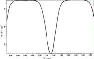
图11A和图11B分别为TCAD模拟的本发明双极晶体管器件结构图和其赝埋层的杂质横向分布图,可以看出,通过浅槽低能量注入的赝埋层在以后的工艺热过程中横向扩散,并在有源区连接,形成埋层,而且杂质上扩到集电区表面的浓度很少,不会影响到双极晶体管的集电区和基区的结击穿电压。而且由于赝埋层注入是高剂量、低能量的注入,赝埋层的浓度较大,而结面积较小,埋层与衬底间的寄生结电容较小。另外由于浅槽底部的埋层浓度较高,过渡金属层Ti/TiN与埋层可形成良好的欧姆接触,保证了深槽接触的集电极有较小的接触电阻。Fig. 11A and Fig. 11B are the bipolar transistor device structure diagram of the present invention simulated by TCAD and the impurity lateral distribution diagram of its pseudo-buried layer respectively. Laterally diffused and connected in the active area to form a buried layer, and the concentration of impurities extended to the surface of the collector area is very small, which will not affect the junction breakdown voltage of the collector area and the base area of the bipolar transistor. Moreover, since the implantation of the pseudo-buried layer is a high-dose, low-energy implantation, the concentration of the pseudo-buried layer is relatively large, but the junction area is small, and the parasitic junction capacitance between the buried layer and the substrate is small. In addition, due to the high concentration of the buried layer at the bottom of the shallow groove, the transition metal layer Ti/TiN and the buried layer can form a good ohmic contact, which ensures that the collector electrode in contact with the deep groove has a small contact resistance.
如图12所示,为TCAD模拟的本发明双极晶体管的器件特性,得到了较高的电流放大系数和特征频率,完全能与现有器件特性相比拟,验证了该器件工艺的可行性。尤其是较高的特征频率表明在没有集电区埋层、集电区外延以及深槽隔离的情况下,本发明双极晶体管仍然具有较低的寄生电容和寄生电阻,从而具备良好的射频特性。As shown in Fig. 12, the device characteristics of the bipolar transistor of the present invention simulated by TCAD obtains a higher current amplification factor and characteristic frequency, which can be completely compared with the existing device characteristics, and verifies the feasibility of the device technology. In particular, the higher characteristic frequency indicates that the bipolar transistor of the present invention still has lower parasitic capacitance and parasitic resistance without collector buried layer, collector extension and deep trench isolation, thereby possessing good radio frequency characteristics .
以上通过具体实施例对本发明进行了详细的说明,但这些并非构成对本发明的限制。在不脱离本发明原理的情况下,本领域的技术人员还可做出许多变形和改进,这些也应视为本发明的保护范围。The present invention has been described in detail through specific examples above, but these do not constitute a limitation to the present invention. Without departing from the principle of the present invention, those skilled in the art can also make many modifications and improvements, which should also be regarded as the protection scope of the present invention.
Claims (4)
Translated fromChinesePriority Applications (2)
| Application Number | Priority Date | Filing Date | Title |
|---|---|---|---|
| CN2009102020117ACN102104062B (en) | 2009-12-21 | 2009-12-21 | bipolar transistor |
| US12/966,241US20110147892A1 (en) | 2009-12-21 | 2010-12-13 | Bipolar Transistor with Pseudo Buried Layers |
Applications Claiming Priority (1)
| Application Number | Priority Date | Filing Date | Title |
|---|---|---|---|
| CN2009102020117ACN102104062B (en) | 2009-12-21 | 2009-12-21 | bipolar transistor |
Publications (2)
| Publication Number | Publication Date |
|---|---|
| CN102104062A CN102104062A (en) | 2011-06-22 |
| CN102104062Btrue CN102104062B (en) | 2012-08-01 |
Family
ID=44149889
Family Applications (1)
| Application Number | Title | Priority Date | Filing Date |
|---|---|---|---|
| CN2009102020117AActiveCN102104062B (en) | 2009-12-21 | 2009-12-21 | bipolar transistor |
Country Status (2)
| Country | Link |
|---|---|
| US (1) | US20110147892A1 (en) |
| CN (1) | CN102104062B (en) |
Families Citing this family (31)
| Publication number | Priority date | Publication date | Assignee | Title |
|---|---|---|---|---|
| CN102117748B (en)* | 2009-12-31 | 2012-06-20 | 上海华虹Nec电子有限公司 | Method for manufacturing collector region and collector region buried layer of bipolar transistor |
| CN102117749B (en)* | 2009-12-31 | 2012-07-11 | 上海华虹Nec电子有限公司 | Manufacturing process of collector region and collector region buried layer of bipolar transistor |
| CN102956480A (en)* | 2011-08-31 | 2013-03-06 | 上海华虹Nec电子有限公司 | Manufacturing method and device for reducing collector resistance through germanium-silicon HBT (Heterojunction Bipolar Transistor) with spuriously buried layer |
| CN102969349B (en)* | 2011-09-01 | 2015-04-08 | 上海华虹宏力半导体制造有限公司 | Transverse parasitic plug-and-play (PNP) device in SiGe heterojunction bipolar transistor (HBT) technique and production method |
| CN102412313B (en)* | 2011-10-14 | 2014-04-16 | 上海华虹宏力半导体制造有限公司 | MOS (metal oxide semiconductor) variable capacitor adopting SiGe HBT (heterojunction bipolar transistor) process and manufacturing method thereof |
| CN103094318B (en)* | 2011-11-03 | 2016-08-17 | 上海华虹宏力半导体制造有限公司 | A kind of SiGe HBT device architecture and manufacture method thereof |
| CN103094229A (en)* | 2011-11-08 | 2013-05-08 | 上海华虹Nec电子有限公司 | Buried layer extraction structure and manufacturing method thereof |
| CN103107188B (en)* | 2011-11-11 | 2015-08-19 | 上海华虹宏力半导体制造有限公司 | Parasitic PNP device structure in a kind of SiGe HBT technique and manufacture method thereof |
| CN103123931B (en)* | 2011-11-21 | 2016-04-13 | 上海华虹宏力半导体制造有限公司 | Parasitic N-I-P type PIN device structure and manufacture method thereof in a kind of BiCMOS technique |
| CN103137676B (en)* | 2011-11-23 | 2016-04-13 | 上海华虹宏力半导体制造有限公司 | A kind of Ge-Si heterojunction bipolar transistor and manufacture method thereof |
| CN103137675B (en)* | 2011-11-23 | 2016-04-13 | 上海华虹宏力半导体制造有限公司 | Ge-Si heterojunction bipolar transistor structure with high-breakdown-voltage and preparation method thereof |
| CN103137663B (en)* | 2011-11-30 | 2015-04-08 | 上海华虹宏力半导体制造有限公司 | Parasitic transversal NPN component and manufacturing method |
| CN103137673B (en)* | 2011-11-30 | 2015-06-03 | 上海华虹宏力半导体制造有限公司 | Self-alignment bipolar transistor and manufacturing method thereof |
| CN103165667B (en)* | 2011-12-09 | 2016-06-08 | 上海华虹宏力半导体制造有限公司 | Vertical parasitic type PNP triode and making method in germanium silicium HBT technique |
| CN103165424B (en)* | 2011-12-13 | 2015-12-16 | 上海华虹宏力半导体制造有限公司 | The method of integrated middle pressure NPN triode in high pressure NPN triode |
| CN103178086B (en)* | 2011-12-21 | 2015-10-14 | 上海华虹宏力半导体制造有限公司 | VPNP device in a kind of SiGe HBT technique and manufacture method thereof |
| CN102522425B (en)* | 2011-12-23 | 2014-04-16 | 上海华虹宏力半导体制造有限公司 | Structure of ultrahigh pressure germanium-silicon heterojunction bipolar transistor (HBT) device and preparation method |
| US20130307122A1 (en)* | 2012-05-16 | 2013-11-21 | Tsinghua University | Bipolar transistor with embedded epitaxial external base region and method of forming the same |
| CN103035576B (en)* | 2012-05-28 | 2014-10-08 | 上海华虹宏力半导体制造有限公司 | Manufacturing method and device structure of germanium silicon heterojunction bipolar transistor (HBT) and complementary metal-oxide-semiconductor transistor (CMOS) device integration |
| CN102800590B (en)* | 2012-08-24 | 2014-09-10 | 中国科学院上海微系统与信息技术研究所 | Preparation method of SOI (silicon on insulator)-based SiGe-HBT (heterojunction bipolar transistor) |
| CN103050493B (en)* | 2012-09-05 | 2015-10-14 | 上海华虹宏力半导体制造有限公司 | Germanium policrystalline silicon Si-gate BiCMOS device and manufacture method |
| CN103871873B (en)* | 2014-04-04 | 2016-09-14 | 哈尔滨工业大学 | Bipolar device radiation hardened method based on launch site geometry |
| US10553633B2 (en)* | 2014-05-30 | 2020-02-04 | Klaus Y.J. Hsu | Phototransistor with body-strapped base |
| FR3087047B1 (en) | 2018-10-08 | 2021-10-22 | St Microelectronics Sa | BIPOLAR TRANSISTOR |
| FR3087048B1 (en) | 2018-10-08 | 2021-11-12 | St Microelectronics Sa | BIPOLAR TRANSISTOR |
| US11374092B2 (en)* | 2019-09-23 | 2022-06-28 | Globalfoundries U.S. Inc. | Virtual bulk in semiconductor on insulator technology |
| FR3113539B1 (en) | 2020-08-24 | 2022-09-23 | St Microelectronics Crolles 2 Sas | bipolar transistor |
| US11881395B2 (en) | 2021-09-01 | 2024-01-23 | Globalfoundries U.S. Inc. | Bipolar transistor structure on semiconductor fin and methods to form same |
| US11843044B2 (en) | 2021-09-29 | 2023-12-12 | Globalfoundries U.S. Inc. | Bipolar transistor structure on semiconductor fin and methods to form same |
| US11749747B2 (en) | 2022-01-13 | 2023-09-05 | Globalfoundries U.S. Inc. | Bipolar transistor structure with collector on polycrystalline isolation layer and methods to form same |
| US12176427B2 (en) | 2022-09-14 | 2024-12-24 | Globalfoundries U.S. Inc. | Bipolar transistor and gate structure on semiconductor fin and methods to form same |
Citations (2)
| Publication number | Priority date | Publication date | Assignee | Title |
|---|---|---|---|---|
| US5455190A (en)* | 1994-12-07 | 1995-10-03 | United Microelectronics Corporation | Method of making a vertical channel device using buried source techniques |
| CN101192537A (en)* | 2006-11-24 | 2008-06-04 | 上海华虹Nec电子有限公司 | Vertical type bipolar transistor manufacture method and vertical type bipolar transistor |
Family Cites Families (6)
| Publication number | Priority date | Publication date | Assignee | Title |
|---|---|---|---|---|
| JP2000252294A (en)* | 1999-03-01 | 2000-09-14 | Nec Corp | Semiconductor device and manufacturing method thereof |
| US6724066B2 (en)* | 2001-04-30 | 2004-04-20 | Texas Instruments Incorporated | High breakdown voltage transistor and method |
| US6770952B2 (en)* | 2001-04-30 | 2004-08-03 | Texas Instruments Incorporated | Integrated process for high voltage and high performance silicon-on-insulator bipolar devices |
| US7136268B2 (en)* | 2004-03-31 | 2006-11-14 | International Business Machines Corporation | Tunable ESD trigger and power clamp circuit |
| JP5096708B2 (en)* | 2006-07-28 | 2012-12-12 | ルネサスエレクトロニクス株式会社 | Semiconductor device and manufacturing method thereof |
| US8217380B2 (en)* | 2008-01-09 | 2012-07-10 | International Business Machines Corporation | Polysilicon emitter BJT access device for PCRAM |
- 2009
- 2009-12-21CNCN2009102020117Apatent/CN102104062B/enactiveActive
- 2010
- 2010-12-13USUS12/966,241patent/US20110147892A1/ennot_activeAbandoned
Patent Citations (2)
| Publication number | Priority date | Publication date | Assignee | Title |
|---|---|---|---|---|
| US5455190A (en)* | 1994-12-07 | 1995-10-03 | United Microelectronics Corporation | Method of making a vertical channel device using buried source techniques |
| CN101192537A (en)* | 2006-11-24 | 2008-06-04 | 上海华虹Nec电子有限公司 | Vertical type bipolar transistor manufacture method and vertical type bipolar transistor |
Non-Patent Citations (1)
| Title |
|---|
| JP平2-90625A 1990.03.30 |
Also Published As
| Publication number | Publication date |
|---|---|
| CN102104062A (en) | 2011-06-22 |
| US20110147892A1 (en) | 2011-06-23 |
Similar Documents
| Publication | Publication Date | Title |
|---|---|---|
| CN102104062B (en) | bipolar transistor | |
| CN102097464B (en) | High-voltage bipolar transistor | |
| CN102231379B (en) | SiGe HBT (Heterojunction Bipolar Transistor) multi-finger structure | |
| JP3494638B2 (en) | Semiconductor device and method of manufacturing semiconductor device | |
| CN206758440U (en) | Positive-negative-positive bipolar transistor | |
| CN102446965B (en) | Germanium-silicon heterojunction bipolar transistor | |
| CN102437180B (en) | Ultra high voltage silicon germanium heterojunction bipolar transistor (HBT) device and manufacturing method thereof | |
| JP2005509273A5 (en) | ||
| US8946041B2 (en) | Methods for forming high gain tunable bipolar transistors | |
| CN102347354A (en) | Germanium-silicon heterojunction bipolar transistor and manufacturing method thereof | |
| US8101491B2 (en) | Heterojunction bipolar transistor | |
| WO2000038227A1 (en) | Method of making a semiconductor device including an asymmetrical field-effect transistor | |
| CN103035689B (en) | Collector region out-leading structure of germanium-silicon heterojunction bipolar transistor (HBT) and manufacturing method thereof | |
| CN102544081B (en) | Silicon germanium heterojunction NPN (negative-positive-negative) triode and manufacture method | |
| CN109545849B (en) | CMOS integrated process BJT structure and its manufacturing method | |
| CN102544079B (en) | Silicon germanium heterojunction NPN (negative-positive-negative) transistor and manufacture method | |
| CN103066101B (en) | Germanium silicium HBT device and manufacture method | |
| US7554174B2 (en) | Bipolar transistor having semiconductor patterns filling contact windows of an insulating layer | |
| CN100533680C (en) | Bipolar transistor and method of manufacturing the same | |
| CN103117300B (en) | Parasitic lateral type PNP device and manufacture method | |
| US8455975B2 (en) | Parasitic PNP bipolar transistor in a silicon-germanium BiCMOS process | |
| US8759880B2 (en) | Ultra-high voltage SIGE HBT device and manufacturing method of the same | |
| CN102412275B (en) | Vertical PNP device in SiGe BiCMOS technology and manufacturing method thereof | |
| CN102386218B (en) | Vertical parasitic PNP device in BiCMOS process and its manufacturing method | |
| CN104425577A (en) | Self-alignment germanium-silicon heterojunction bipolar triode device and manufacturing method thereof |
Legal Events
| Date | Code | Title | Description |
|---|---|---|---|
| C06 | Publication | ||
| PB01 | Publication | ||
| C10 | Entry into substantive examination | ||
| SE01 | Entry into force of request for substantive examination | ||
| C14 | Grant of patent or utility model | ||
| GR01 | Patent grant | ||
| ASS | Succession or assignment of patent right | Owner name:SHANGHAI HUAHONG GRACE SEMICONDUCTOR MANUFACTURING Free format text:FORMER OWNER: HUAHONG NEC ELECTRONICS CO LTD, SHANGHAI Effective date:20131218 | |
| C41 | Transfer of patent application or patent right or utility model | ||
| COR | Change of bibliographic data | Free format text:CORRECT: ADDRESS; FROM: 201206 PUDONG NEW AREA, SHANGHAI TO: 201203 PUDONG NEW AREA, SHANGHAI | |
| TR01 | Transfer of patent right | Effective date of registration:20131218 Address after:201203 Shanghai city Zuchongzhi road Pudong New Area Zhangjiang hi tech Park No. 1399 Patentee after:Shanghai Huahong Grace Semiconductor Manufacturing Corporation Address before:201206, Shanghai, Pudong New Area, Sichuan Road, No. 1188 Bridge Patentee before:Shanghai Huahong NEC Electronics Co., Ltd. |