CN102099932B - Light emitting device package, back-light unit, and liquid crystal display device using the same - Google Patents
Light emitting device package, back-light unit, and liquid crystal display device using the sameDownload PDFInfo
- Publication number
- CN102099932B CN102099932BCN2008801303752ACN200880130375ACN102099932BCN 102099932 BCN102099932 BCN 102099932BCN 2008801303752 ACN2008801303752 ACN 2008801303752ACN 200880130375 ACN200880130375 ACN 200880130375ACN 102099932 BCN102099932 BCN 102099932B
- Authority
- CN
- China
- Prior art keywords
- lens
- depression
- light emitting
- emitting device
- luminescent device
- Prior art date
- Legal status (The legal status is an assumption and is not a legal conclusion. Google has not performed a legal analysis and makes no representation as to the accuracy of the status listed.)
- Active
Links
Images


Classifications
- H—ELECTRICITY
- H10—SEMICONDUCTOR DEVICES; ELECTRIC SOLID-STATE DEVICES NOT OTHERWISE PROVIDED FOR
- H10H—INORGANIC LIGHT-EMITTING SEMICONDUCTOR DEVICES HAVING POTENTIAL BARRIERS
- H10H20/00—Individual inorganic light-emitting semiconductor devices having potential barriers, e.g. light-emitting diodes [LED]
- H10H20/80—Constructional details
- H10H20/85—Packages
- H10H20/852—Encapsulations
- H10H20/853—Encapsulations characterised by their shape
- G—PHYSICS
- G02—OPTICS
- G02F—OPTICAL DEVICES OR ARRANGEMENTS FOR THE CONTROL OF LIGHT BY MODIFICATION OF THE OPTICAL PROPERTIES OF THE MEDIA OF THE ELEMENTS INVOLVED THEREIN; NON-LINEAR OPTICS; FREQUENCY-CHANGING OF LIGHT; OPTICAL LOGIC ELEMENTS; OPTICAL ANALOGUE/DIGITAL CONVERTERS
- G02F1/00—Devices or arrangements for the control of the intensity, colour, phase, polarisation or direction of light arriving from an independent light source, e.g. switching, gating or modulating; Non-linear optics
- G02F1/01—Devices or arrangements for the control of the intensity, colour, phase, polarisation or direction of light arriving from an independent light source, e.g. switching, gating or modulating; Non-linear optics for the control of the intensity, phase, polarisation or colour
- G02F1/13—Devices or arrangements for the control of the intensity, colour, phase, polarisation or direction of light arriving from an independent light source, e.g. switching, gating or modulating; Non-linear optics for the control of the intensity, phase, polarisation or colour based on liquid crystals, e.g. single liquid crystal display cells
- G02F1/133—Constructional arrangements; Operation of liquid crystal cells; Circuit arrangements
- G02F1/1333—Constructional arrangements; Manufacturing methods
- G02F1/1335—Structural association of cells with optical devices, e.g. polarisers or reflectors
- G02F1/1336—Illuminating devices
- G02F1/133602—Direct backlight
- G02F1/133603—Direct backlight with LEDs
- H—ELECTRICITY
- H01—ELECTRIC ELEMENTS
- H01L—SEMICONDUCTOR DEVICES NOT COVERED BY CLASS H10
- H01L2224/00—Indexing scheme for arrangements for connecting or disconnecting semiconductor or solid-state bodies and methods related thereto as covered by H01L24/00
- H01L2224/01—Means for bonding being attached to, or being formed on, the surface to be connected, e.g. chip-to-package, die-attach, "first-level" interconnects; Manufacturing methods related thereto
- H01L2224/42—Wire connectors; Manufacturing methods related thereto
- H01L2224/47—Structure, shape, material or disposition of the wire connectors after the connecting process
- H01L2224/48—Structure, shape, material or disposition of the wire connectors after the connecting process of an individual wire connector
- H01L2224/4805—Shape
- H01L2224/4809—Loop shape
- H01L2224/48091—Arched
- H—ELECTRICITY
- H01—ELECTRIC ELEMENTS
- H01L—SEMICONDUCTOR DEVICES NOT COVERED BY CLASS H10
- H01L2224/00—Indexing scheme for arrangements for connecting or disconnecting semiconductor or solid-state bodies and methods related thereto as covered by H01L24/00
- H01L2224/01—Means for bonding being attached to, or being formed on, the surface to be connected, e.g. chip-to-package, die-attach, "first-level" interconnects; Manufacturing methods related thereto
- H01L2224/42—Wire connectors; Manufacturing methods related thereto
- H01L2224/47—Structure, shape, material or disposition of the wire connectors after the connecting process
- H01L2224/48—Structure, shape, material or disposition of the wire connectors after the connecting process of an individual wire connector
- H01L2224/481—Disposition
- H01L2224/48151—Connecting between a semiconductor or solid-state body and an item not being a semiconductor or solid-state body, e.g. chip-to-substrate, chip-to-passive
- H01L2224/48221—Connecting between a semiconductor or solid-state body and an item not being a semiconductor or solid-state body, e.g. chip-to-substrate, chip-to-passive the body and the item being stacked
- H01L2224/48245—Connecting between a semiconductor or solid-state body and an item not being a semiconductor or solid-state body, e.g. chip-to-substrate, chip-to-passive the body and the item being stacked the item being metallic
- H01L2224/48247—Connecting between a semiconductor or solid-state body and an item not being a semiconductor or solid-state body, e.g. chip-to-substrate, chip-to-passive the body and the item being stacked the item being metallic connecting the wire to a bond pad of the item
- H—ELECTRICITY
- H01—ELECTRIC ELEMENTS
- H01L—SEMICONDUCTOR DEVICES NOT COVERED BY CLASS H10
- H01L25/00—Assemblies consisting of a plurality of semiconductor or other solid state devices
- H01L25/03—Assemblies consisting of a plurality of semiconductor or other solid state devices all the devices being of a type provided for in a single subclass of subclasses H10B, H10D, H10F, H10H, H10K or H10N, e.g. assemblies of rectifier diodes
- H01L25/04—Assemblies consisting of a plurality of semiconductor or other solid state devices all the devices being of a type provided for in a single subclass of subclasses H10B, H10D, H10F, H10H, H10K or H10N, e.g. assemblies of rectifier diodes the devices not having separate containers
- H01L25/075—Assemblies consisting of a plurality of semiconductor or other solid state devices all the devices being of a type provided for in a single subclass of subclasses H10B, H10D, H10F, H10H, H10K or H10N, e.g. assemblies of rectifier diodes the devices not having separate containers the devices being of a type provided for in group H10H20/00
- H01L25/0753—Assemblies consisting of a plurality of semiconductor or other solid state devices all the devices being of a type provided for in a single subclass of subclasses H10B, H10D, H10F, H10H, H10K or H10N, e.g. assemblies of rectifier diodes the devices not having separate containers the devices being of a type provided for in group H10H20/00 the devices being arranged next to each other
Landscapes
- Planar Illumination Modules (AREA)
- Led Device Packages (AREA)
Abstract
Description
Translated fromChinese技术领域technical field
本发明涉及发光器件封装、以及背光单元、以及使用它们的液晶显示装置。 The present invention relates to a light emitting device package, and a backlight unit, and a liquid crystal display device using them. the
背景技术Background technique
液晶显示(LCD)装置是一种将基于图像信息的数据信号单独地施加到布置成矩阵的像素以由此调整像素的光透射率从而能够显示期望的图像的显示装置。这样的LCD装置不具有自发光功能,因此被设计为在设置在其背面的背光单元的辅助下显示图像。 A liquid crystal display (LCD) device is a display device that individually applies data signals based on image information to pixels arranged in a matrix to thereby adjust light transmittance of the pixels so as to be able to display a desired image. Such LCD devices do not have a self-illumination function, and thus are designed to display images with the assistance of a backlight unit disposed on the rear thereof. the
近来,发光二极管(LED)已被用作用于LCD的背光单元的光源。使用LED的背光单元的应用逐渐扩展到用于膝上型计算机以及手机等的LCD。 Recently, light emitting diodes (LEDs) have been used as light sources for backlight units of LCDs. Applications of backlight units using LEDs are gradually expanding to LCDs for laptop computers, mobile phones, and the like. the
使用LED的背光单元可被分为如图1中所示的光导板(LGP)型、以及图2中所示的直接型。 Backlight units using LEDs may be classified into a light guide plate (LGP) type as shown in FIG. 1 and a direct type as shown in FIG. 2 . the
如图1中所示的光导板型背光单元被设计为使得从LED封装1发出的光穿过光导板2的侧面,从而实现亮度均匀性。 The light guide plate type backlight unit as shown in FIG. 1 is designed such that light emitted from the LED package 1 passes through the side of the
如图2中所示的直接型背光单元被设计为使得LED封装3以固定间距设置在散射板4下方,从而实现亮度均匀性。直接型背光单元通常使用视角为120°的LED封装。 The direct type backlight unit as shown in FIG. 2 is designed such that the LED packages 3 are disposed under the
发明内容Contents of the invention
本发明涉及一种发光器件封装。本发明还涉及一种背光单元和使用该背光单元的液晶显示装置。本发明还涉及一种使用该发光器件封装或者背光单元的液晶显示装置。 The invention relates to a light emitting device package. The invention also relates to a backlight unit and a liquid crystal display device using the backlight unit. The invention also relates to a liquid crystal display device using the light emitting device package or a backlight unit. the
在一种实施方式中,所述发光器件封装包括:封装主体;安装在所述封装主体上的发光器件;包含在所述封装主体内并与所述发光器件电连接 的至少一对引线;以及位于所述封装主体的所述发光器件上方的透镜,该透镜具有从该透镜的上表面凹进去的凹陷和在所述凹陷周围限定以具有至少一个曲率半径的弯曲的上表面。从所述发光器件到所述凹陷的最低部分的最短距离大于D1/7且小于D1/2.4,其中D1是所述透镜的直径。 In one embodiment, the light emitting device package includes: a package body; a light emitting device mounted on the package body; at least a pair of leads contained in the package body and electrically connected to the light emitting device; and A lens located above the light emitting device of the package body, the lens having a depression recessed from an upper surface of the lens and a curved upper surface defined around the depression to have at least one radius of curvature. A shortest distance from the light emitting device to the lowest portion of the recess is greater than D1/7 and less than D1/2.4, where D1 is the diameter of the lens. the
在另一实施方式中,所述发光器件封装包括:封装主体;安装在所述封装主体上的发光器件;包含在所述封装主体内并与所述发光器件电连接的至少一对引线;以及位于所述封装主体的所述发光器件上方的透镜,该透镜具有从该透镜的上表面凹进去的凹陷和在所述凹陷周围限定以具有至少一个曲率半径的弯曲的上表面。所述透镜的弯曲的上表面的曲率半径大于0.8mm且小于1.8mm。 In another embodiment, the light emitting device package includes: a package body; a light emitting device mounted on the package body; at least a pair of leads contained in the package body and electrically connected to the light emitting device; and A lens located above the light emitting device of the package body, the lens having a depression recessed from an upper surface of the lens and a curved upper surface defined around the depression to have at least one radius of curvature. The curved upper surface of the lens has a radius of curvature greater than 0.8mm and less than 1.8mm. the
发光器件封装的又一实施方式包括:封装主体;安装在所述封装主体上的发光器件;与所述发光器件电连接的至少一对引线;以及位于所述封装主体的所述发光器件上方的透镜,该透镜具有从该透镜的上表面凹进去的凹陷和在所述凹陷周围限定以具有至少一个曲率半径的弯曲的上表面。从所述发光器件到所述凹陷的最低部分的最短距离大于D1/7且小于D1/2.4,其中D1是所述透镜的直径,并且所述透镜的弯曲的上表面的曲率半径大于0.8mm且小于1.8mm。 Another embodiment of the light emitting device package includes: a package body; a light emitting device mounted on the package body; at least a pair of leads electrically connected to the light emitting device; A lens having a depression recessed from an upper surface of the lens and a curved upper surface defined around the depression to have at least one radius of curvature. The shortest distance from the light emitting device to the lowest portion of the recess is greater than D1/7 and less than D1/2.4, where D1 is the diameter of the lens, and the curved upper surface of the lens has a radius of curvature greater than 0.8mm and Less than 1.8mm. the
在背光单元的一种实施方式中,所述背光单元包括发光器件封装、以及其上布置和安装多个所述发光器件封装的电路板。所述发光器件封装包括:安装在封装主体上的发光器件;以及位于所述封装主体的所述发光器件上方的透镜,该透镜具有从该透镜的上表面凹进去的凹陷和在所述凹陷周围限定以具有至少一个曲率半径的弯曲的上表面。从所述发光器件到所述凹陷的最低部分的最短距离大于D1/7且小于D1/2.4,其中D1是所述透镜的直径。 In one embodiment of the backlight unit, the backlight unit includes a light emitting device package, and a circuit board on which a plurality of the light emitting device packages are arranged and mounted. The light emitting device package includes: a light emitting device mounted on a package body; and a lens located above the light emitting device of the package body, the lens having a depression recessed from an upper surface of the lens and surrounding the depression. A curved upper surface is defined having at least one radius of curvature. A shortest distance from the light emitting device to the lowest portion of the recess is greater than D1/7 and less than D1/2.4, where D1 is the diameter of the lens. the
在背光单元的另一实施方式中,所述背光单元包括发光器件封装、以及其上布置和安装多个所述发光器件封装的电路板。所述发光器件封装包括:安装在封装主体上的发光器件;以及位于所述封装主体的所述发光器件上方的透镜,该透镜具有从该透镜的上表面凹进去的凹陷和在所述凹陷周围限定以具有至少一个曲率半径的弯曲的上表面。所述透镜的弯曲的上表面的曲率半径大于0.8mm且小于1.8mm。 In another embodiment of the backlight unit, the backlight unit includes a light emitting device package, and a circuit board on which a plurality of the light emitting device packages are arranged and mounted. The light emitting device package includes: a light emitting device mounted on a package body; and a lens located above the light emitting device of the package body, the lens having a depression recessed from an upper surface of the lens and surrounding the depression. A curved upper surface is defined having at least one radius of curvature. The curved upper surface of the lens has a radius of curvature greater than 0.8mm and less than 1.8mm. the
背光单元的又一实施方式包括发光器件封装、以及其上布置和安装多个所述发光器件封装的电路板。所述发光器件封装包括:安装在封装主体上的发光器件;以及位于所述封装主体的所述发光器件上方的透镜,该透镜具有从该透镜的上表面凹进去的凹陷和在所述凹陷周围限定以具有至少一个曲率半径的弯曲的上表面。从所述发光器件到所述凹陷的最低部分的最短距离大于D1/7且小于D1/2.4,其中D1是所述透镜的直径,并且所述透镜的弯曲的上表面的曲率半径大于0.8mm且小于1.8mm。Still another embodiment of a backlight unit includes a light emitting device package, and a circuit board on which a plurality of the light emitting device packages are arranged and mounted. The light emitting device package includes: a light emitting device mounted on a package body; and a lens located above the light emitting device of the package body, the lens having a depression recessed from an upper surface of the lens and surrounding the depression. A curved upper surface is defined having at least one radius of curvature. The shortest distance from the light emitting device to the lowest portion of the recess is greater than D1/7 and less than D1/2.4, where D1 is the diameter of the lens, and the curved upper surface of the lens has a radius of curvature greater than 0.8mm and Less than 1.8mm.
液晶显示装置的一种实施方式包括:发光器件封装,所述发光器件封装包括安装在封装主体上的发光器件;背光单元,所述背光单元包括其上布置和安装多个所述发光器件封装的电路板;以及位于所述背光单元上的液晶板。所述发光器件封装包括位于所述封装主体的所述发光器件上方的透镜,该透镜具有从该透镜的上表面凹进去的凹陷和在所述凹陷周围限定以具有至少一个曲率半径的弯曲的上表面,从所述发光器件到所述凹陷的最低部分的最短距离大于D1/7且小于D1/2.4,其中D1是所述透镜的直径,并且所述透镜的弯曲的上表面的曲率半径大于0.8mm且小于1.8mm。 An embodiment of a liquid crystal display device includes: a light emitting device package including a light emitting device mounted on a package main body; a backlight unit including a light emitting device package on which a plurality of the light emitting device packages are arranged and mounted. a circuit board; and a liquid crystal panel on the backlight unit. The light emitting device package includes a lens above the light emitting device of the package body, the lens having a depression recessed from an upper surface of the lens and a curved upper surface defined around the depression to have at least one radius of curvature. a surface, the shortest distance from the light emitting device to the lowest portion of the depression is greater than D1/7 and less than D1/2.4, where D1 is the diameter of the lens, and the curved upper surface of the lens has a radius of curvature greater than 0.8 mm and less than 1.8mm. the
应当理解,本发明的上述概括描述和下述详细描述均是示例性和说明性的,且旨在提供对所请求保护的本发明的进一步说明。 It is to be understood that both the foregoing general description and the following detailed description of the present invention are exemplary and explanatory and are intended to provide further explanation of the invention as claimed. the
附图说明Description of drawings
包含附图以提供对本发明的进一步理解,附图被结合到本申请文件中并构成本申请文件的一部分,附图图示本发明的实施方式,并与说明书一起用于解释本发明的原理。附图中: The accompanying drawings are included to provide a further understanding of the invention, and are incorporated in and constitute a part of this specification, illustrate embodiments of the invention and together with the description serve to explain the principle of the invention. In the attached picture:
图1是图示光导板型背光单元的一个示例的示意图; FIG. 1 is a schematic diagram illustrating an example of a light guide plate type backlight unit;
图2是图示直接型背光单元的一个示例的示意图; 2 is a schematic diagram illustrating an example of a direct type backlight unit;
图3是图示发光器件的观察图案的图; 3 is a diagram illustrating an observation pattern of a light emitting device;
图4是图示常规的发光器件的观察图案的图; 4 is a diagram illustrating an observation pattern of a conventional light emitting device;
图5是图示用于实现亮度均匀性的观察图案的图; 5 is a diagram illustrating an observation pattern for achieving brightness uniformity;
图6A和图6B是图示背光单元的发光器件基于视角的布置的示意图; 6A and 6B are schematic diagrams illustrating the arrangement of light emitting devices of a backlight unit based on viewing angles;
图7A和图8A是图示基于中心发光强度的观察图案的图; 7A and 8A are diagrams illustrating observation patterns based on central luminous intensity;
图7B和图8B是图示基于中心发光强度的光图案的图; 7B and 8B are diagrams illustrating light patterns based on central luminous intensity;
图9A到图10B是图示基于观察图案的变化的光图案的图; 9A to 10B are diagrams illustrating light patterns based on changes in observed patterns;
图11是图示根据本发明的发光器件封装的一种实施方式的截面图; 11 is a cross-sectional view illustrating an embodiment of a light emitting device package according to the present invention;
图12A到图13C是图示基于从LED到透镜中心的距离D2的变化的示意图; 12A to 13C are schematic diagrams illustrating variations based on distance D2 from the LED to the center of the lens;
图14A和图14B是图示当D2等于D1/2.5时发光器件封装的亮度分布和观察图案的视图; 14A and 14B are views illustrating the luminance distribution and observation pattern of a light emitting device package when D2 is equal to D1/2.5;
图15A和图15B是图示当D2等于D1/7.1时发光器件封装的亮度分布和观察图案的视图; 15A and 15B are views illustrating the luminance distribution and observation pattern of a light emitting device package when D2 is equal to D1/7.1;
图16A和图16B是图示当D2等于D1/3时发光器件封装的亮度分布和观察图案的视图; 16A and 16B are views illustrating the luminance distribution and observation pattern of a light emitting device package when D2 is equal to D1/3;
图17A和图17B是图示当D2等于D1/3.85时发光器件封装的亮度分布和观察图案的视图; 17A and 17B are views illustrating the luminance distribution and observation pattern of a light emitting device package when D2 is equal to D1/3.85;
图18A和图18B是图示基于曲率半径R的视角的图; 18A and 18B are diagrams illustrating a viewing angle based on a radius of curvature R;
图19A和图19B是图示当R是1.8mm时发光器件封装的亮度分布和观察图案的视图; 19A and 19B are views illustrating luminance distribution and observation patterns of a light emitting device package when R is 1.8 mm;
图20A和图20B是图示当R是0.8mm时发光器件封装的亮度分布和观察图案的视图; 20A and 20B are views illustrating the luminance distribution and observation pattern of a light emitting device package when R is 0.8 mm;
图21A和图21B是图示当R是1.0mm时发光器件封装的亮度分布和观察图案的视图; 21A and 21B are views illustrating luminance distribution and observation patterns of a light emitting device package when R is 1.0 mm;
图22A和图22B是图示当R是1.6mm时发光器件封装的亮度分布和观察图案的视图; 22A and 22B are views illustrating the luminance distribution and observation pattern of a light emitting device package when R is 1.6mm;
图23A和图23B是图示基于中心凹陷角θ的光分布的示意图; 23A and 23B are schematic diagrams illustrating the light distribution based on the central depression angle θ;
图24A和图24B是图示当角θ是90°时发光器件封装的亮度分布和观察图案的视图; 24A and 24B are views illustrating the luminance distribution and observation pattern of a light emitting device package when the angle θ is 90°;
图25A和图25B是图示当角θ是120°时发光器件封装的亮度分布和观察图案的视图; 25A and 25B are views illustrating the luminance distribution and observation pattern of a light emitting device package when the angle θ is 120°;
图26A和图26B是图示当角θ是100°时发光器件封装的亮度分布和观察图案的视图; 26A and 26B are views illustrating the luminance distribution and observation pattern of a light emitting device package when the angle θ is 100°;
图27A和图27B是图示当角θ是110°时发光器件封装的亮度分布和观察图案的视图; 27A and 27B are views illustrating the luminance distribution and observation pattern of a light emitting device package when the angle θ is 110°;
图28是图示基于最佳中心凹陷角的光的行进的示意图; FIG. 28 is a schematic diagram illustrating the travel of light based on an optimal central notch angle;
图29是图示透镜的一种实施方式的截面图; Figure 29 is a cross-sectional view illustrating one embodiment of a lens;
图30是图示发光器件封装的截面图; 30 is a cross-sectional view illustrating a light emitting device package;
图31是图示透镜的另一实施方式的截面图; Figure 31 is a cross-sectional view illustrating another embodiment of a lens;
图32是图示发光器件封装的另一实施方式的截面图; 32 is a cross-sectional view illustrating another embodiment of a light emitting device package;
图33是图示发光器件封装的又一实施方式的截面图; 33 is a cross-sectional view illustrating yet another embodiment of a light emitting device package;
图34是图示液晶显示装置的一个示例的分解视图; FIG. 34 is an exploded view illustrating an example of a liquid crystal display device;
图35是图示液晶显示板的一个示例的截面图;以及 Figure 35 is a sectional view illustrating an example of a liquid crystal display panel; and
图36是图示包括液晶显示装置的液晶显示电视机的框图。 FIG. 36 is a block diagram illustrating a liquid crystal display television including a liquid crystal display device. the
具体实施方式Detailed ways
下面将详细描述本发明的优选实施方式,在附图中图示出其示例。在整个附图中尽量使用相同的附图标记表示相同或相似的部件。 Reference will now be made in detail to the preferred embodiments of the invention, examples of which are illustrated in the accompanying drawings. Wherever possible, the same reference numbers will be used throughout the drawings to refer to the same or like parts. the
本发明可以具有各种修改和替换形式,其具体的实施方式在附图中通过示例方式示出并在此将详细描述。然而,应理解,无意将本发明限制于所公开的特定形式,相反地,本发明将覆盖落在如所附权利要求限定的本发明的精神和范围内的全部修改、等同方案以及替型。 While the invention is capable of various modifications and alternative forms, specific embodiments thereof are shown by way of example in the drawings and will be described in detail herein. It should be understood, however, that there is no intent to limit the invention to the particular forms disclosed, but on the contrary, the invention is to cover all modifications, equivalents, and alternatives falling within the spirit and scope of the invention as defined by the appended claims. the
应理解,当比如层、区域或衬底等元件被称为在其它元件“上”时,其可以直接位于该其它元件上或者也可能存在中间元件。 It will be understood that when an element such as a layer, region or substrate is referred to as being "on" another element, it can be directly on the other element or intervening elements may also be present. the
应理解,这些术语意在除附图中描绘的方向之外,还要包含各种器件方向。最后,术语“直接”指没有中间元件。如在此所用的,术语“和/或”包括所列举的相关术语中的一个或多个术语的任意和全部的组合。 It is to be understood that these terms are intended to encompass various device orientations in addition to the orientation depicted in the figures. Finally, the term "directly" means without intervening elements. As used herein, the term "and/or" includes any and all combinations of one or more of the associated listed terms. the
在厚度固定的背光单元(BLU)的配置中,考虑到图3所示的LED与位置E和E′之间的位置关系,每个位置的亮度变化如下列等式1所示。在下列等式1中,E′表示末端位置处的发光强度,而E表示起始位置处的发光强度。 In the configuration of a backlight unit (BLU) with a fixed thickness, considering the positional relationship between LEDs and positions E and E' shown in FIG. In the following Equation 1, E' represents the luminescence intensity at the end position, and E represents the luminescence intensity at the start position. the
[等式1] [equation 1]
E′=E×COS3θ E'=E×COS3 θ
如果E′和E相同,则实现适合于背光单元的亮度均匀性。为了实现亮度均匀性,每个位置的发光强度必须为如图5中所示。 If E' and E are the same, brightness uniformity suitable for a backlight unit is achieved. In order to achieve brightness uniformity, the luminous intensity at each location must be as shown in Figure 5. the
具体地,如从图示观察图案的图5中可看出的,为了实现亮度均匀性, LED的中心部分(由为0°的角θ指示)必须具有低发光强度,并且发光强度必须随着角θ增大而增大。 Specifically, as can be seen from FIG. 5 illustrating the observation pattern, in order to achieve brightness uniformity, the central portion of the LED (indicated by the angle θ being 0°) must have a low luminous intensity, and the luminous intensity must increase with Angle θ increases and increases. the
这是因为发光强度能够由下列等式2表示。 This is because the luminous intensity can be represented by
[等式2] [equation 2]
E′=E×d E'=E×d
其中,E′表示末端位置处的发光强度,E表示起始位置处的发光强度,以及d表示光的行进距离。 Here, E' represents the luminous intensity at the end position, E represents the luminous intensity at the starting position, and d represents the travel distance of the light. the
本发明具有以下特征:形成具有针对LED的特定形状的透镜,以便获得如图5中示出的观察图案;以及以特定间距布置基于上述结果形成的一个或者多个LED,由此在从这些LED的上平面起的预定距离处实现亮度均匀性。 The present invention has the following features: forming a lens having a specific shape for the LEDs so as to obtain an observation pattern as shown in FIG. 5; Brightness uniformity is achieved at a predetermined distance from the upper plane of the the
为了获得如图5中示出的观察图案,透镜的设计必须满足以下三个重要设计目标。 In order to obtain the observed pattern as shown in Fig. 5, the design of the lens must satisfy the following three important design goals. the
首先,视角必须最大化。 First, the viewing angle must be maximized. the
当使用具有120°的视角的常规LED封装10基于朗伯(Lambertian)分布来构建背光单元时,可以如图6A中所示的相对于散射板20来布置LED封装10。 When constructing a backlight unit based on a Lambertian distribution using conventional LED packages 10 having a viewing angle of 120°, the LED packages 10 may be arranged relative to the
然而,对于背光单元中LED的布置,视角必须比120°更广,以使LED的数量最小化并减小背光单元的厚度。这样的比120°更广的视角可能造成如图6B中所示的封装布置。 However, for the arrangement of LEDs in the backlight unit, the viewing angle must be wider than 120° in order to minimize the number of LEDs and reduce the thickness of the backlight unit. Such a wider viewing angle than 120° may result in a package arrangement as shown in Figure 6B. the
第二,LED中心处的发光强度分布必须小于最大强度分布。 Second, the luminous intensity distribution at the center of the LED must be smaller than the maximum intensity distribution. the
当尽管视角广,但LED中心的发光强度分布还是宽时,LED中心呈现出极其高的亮度。这样的亮度分布造成热点(hot spot),导致亮度均匀性变差。 When the luminous intensity distribution in the center of the LED is wide despite the wide viewing angle, the center of the LED exhibits extremely high brightness. Such luminance distribution causes hot spots, resulting in poor luminance uniformity. the
更具体而言,如图7A中所示,当LED封装在其中心处具有基于宽发光强度分布的视角时,亮度均匀性可能变差,如图7B中所示(中心黑色区域表示光聚集的区域)。然而,当LED封装在其中心处具有基于窄发光强度分布的视角时,亮度均匀性能够获得很大的增强,如图8B中所示。 More specifically, as shown in FIG. 7A, when the LED package has a viewing angle at its center based on a wide luminous intensity distribution, brightness uniformity may deteriorate, as shown in FIG. area). However, when the LED package has a viewing angle at its center based on a narrow luminous intensity distribution, the luminance uniformity can be greatly enhanced, as shown in FIG. 8B . the
应注意,在图7A中示出的数值指示极坐标中的视角,在下文中,在图示观察图案的附图中示出的全部数值都指示极坐标中的视角。 It should be noted that the numerical values shown in FIG. 7A indicate the viewing angles in polar coordinates, and hereinafter, all numerical values shown in the drawings illustrating observation patterns indicate the viewing angles in polar coordinates. the
第三,整个视角分布必须具有平缓的变化。 Third, the entire viewing angle distribution must have a gradual change. the
即使视角广并且有效地控制中心处的发光强度分布,但当视角不具有平缓的形状变化时还是可能出现环形暗区。 Even though the viewing angle is wide and the luminous intensity distribution at the center is effectively controlled, an annular dark area may appear when the viewing angle does not have a gentle shape change. the
具体而言,如图9A中所示,当观察图案不具有平缓变化时,如图9B中所示出现环形图案,从而导致亮度均匀性变差。然而,当观察图案具有如图10A中所示的平缓变化时,能够实现如图10B中所示的增强的亮度均匀性。 Specifically, as shown in FIG. 9A , when the observation pattern does not have a gentle change, a circular pattern appears as shown in FIG. 9B , resulting in deterioration of brightness uniformity. However, when the observation pattern has a gentle change as shown in FIG. 10A , enhanced brightness uniformity as shown in FIG. 10B can be achieved. the
下面,将参照图11描述获得最佳观察图案的发光器件封装和透镜的配置。 Next, a configuration of a light emitting device package and a lens for obtaining an optimum viewing pattern will be described with reference to FIG. 11 . the
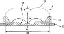
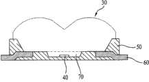
LED芯片40安装在发光器件封装主体50上,继而透镜30安装在LED芯片40上。封装主体50设置有与LED芯片40电连接的引线60。引线60可以布置在封装主体50的外部或下方位置。 The
在LED芯片40的上方的透镜30具有从其上表面凹进去的凹陷,并且透镜30的上表面从凹陷处向外弯曲。该上表面延伸到透镜30的侧表面,并且透镜30的与该上表面相对的表面是透镜30的下表面。 The
或者,透镜30可以通过在其上安装了LED芯片40的封装主体50上注入透镜材料来直接形成。在此情况下,在LED芯片40和透镜30之间不会存在由于粘合剂或者别的材料导致的界面。使透镜30与LED芯片40直接接触能够消除不必要的反射和折射现象,从而实现光学性能上的提高。 Alternatively, the
在本发明中,可以在封装主体50上安装两个或者更多个LED芯片40,相应地,引线60的数量可随LED芯片40的数量而增加。所述两个或者更多个LED芯片40可以具有不同颜色,或者可以具有相同颜色以增强发光强度。 In the present invention, two or
封装主体50被形成为具有用于安装LED芯片40的槽。 The
如必要时,可以在透镜30和封装主体50之间填充封装材料70。封装材料可以是硅酮或者环氧树脂。当封装主体被形成为具有安装槽时,在安装槽中填充封装材料70。 If necessary, an
必要时,封装材料70可以包含荧光体(或散射体),以将从LED芯片40发出的光的波长改变为白色或者其它颜色的波长波段。封装材料70还可以起LED芯片40的保护层的作用。 If necessary, the
荧光体(或者散射体)可以从包括黄色、绿色、红色以及橙色荧光体等的多种荧光体中选择。 Phosphors (or scatterers) can be selected from a variety of phosphors including yellow, green, red, and orange phosphors, among others. the
可以通过使用打底剂或者其它粘性二次材料来将透镜30附接到封装主体50。如果封装材料70和透镜30由相同材料制成,则即使不使用二次粘合剂也能够附接透镜30。 The
或者,可以通过传递模塑或者注入模塑来形成透镜30,并直接将其附接到封装主体50。 Alternatively, the
在此情况下,如果透镜30被设计为形状上满足以下基本要素,则透镜30能够实现期望的观察图案。当透镜30被制造为具有根据以下基本要素的本发明建议的形状时,能够实现增强的亮度均匀性,从而获得的背光单元能够表现出提高的产品质量。 In this case, if the
用于确定透镜30的形状的基本要素包括从作为光源的LED芯片40到透镜30的中心的最低部分的距离D2、透镜30的曲率半径、以及透镜30的中心凹陷的角θ。 Basic elements for determining the shape of the
在下文,将详细描述确定基本要素D2、R以及θ的范围以确定透镜30的形状的方法。 Hereinafter, a method of determining the ranges of the basic elements D2, R, and θ to determine the shape of the
<从LED芯片到透镜中心的最低部分的最短距离的确定> <Determination of the shortest distance from the LED chip to the lowest part of the lens center>
首先,如果距离D2明显很短,则如图12A中所示,通过中心凹陷发出大量的光,且视角如图12B中所示地变化。结果,当使用上述发光器件封装来制造背光单元时,在背光单元的中心出现如图12C中所示的热点。 First, if the distance D2 is significantly short, then as shown in Figure 12A, a large amount of light is emitted through the central depression, and the viewing angle changes as shown in Figure 12B. As a result, when a backlight unit was manufactured using the above light emitting device package, a hot spot as shown in FIG. 12C occurred at the center of the backlight unit. the
如果距离D2明显很长,则如图13A中所示,通过透镜30的中心凹陷发出极其少的光,且视角如图13B中所示地变化。结果,获得的背光单元呈现出暗区(图13C)。 If the distance D2 is significantly long, then as shown in Figure 13A, very little light is emitted through the central depression of the
如上所述,距离D2指示LED芯片40与透镜30的中心凹陷之间的最短距离。为了给获得的背光单元提供最佳观察特性,距离D2必须在预定范围内。 As described above, the distance D2 indicates the shortest distance between the
接着,将不完全地描述发光器件封装随距离D2的变化的亮度分布和观察图案。 Next, the luminance distribution and observation pattern of the light emitting device package as a function of the distance D2 will be described incompletely. the
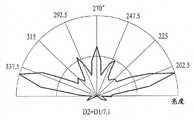
图14A和图14B图示当距离D2等于D1/2.5时发光器件封装的亮度分布和观察图案。在此,D1表示透镜30的直径。 14A and 14B illustrate the luminance distribution and observation pattern of the light emitting device package when the distance D2 is equal to D1/2.5. Here, D1 represents the diameter of the
图15A和图15B图示当距离D2等于D1/7.1时发光器件封装的亮度分布和观察图案。 15A and 15B illustrate the luminance distribution and observation pattern of the light emitting device package when the distance D2 is equal to D1/7.1. the
如从以上描述可理解到的,当距离D2具有D1/2.5的相对大的值时,如图14A中所示,明亮区域处于周围,而宽暗区出现在中心。 As can be understood from the above description, when the distance D2 has a relatively large value of D1/2.5, as shown in FIG. 14A , a bright area is around and a wide dark area appears at the center. the
另外,可理解,当距离D2具有D1/7.1的相对小的值时,通过中心凹陷发出大量的光,如图15B中所示造成亮度分布聚集在中心,从而造成如图15A中所示的热点。 In addition, it can be understood that when the distance D2 has a relatively small value of D1/7.1, a large amount of light is emitted through the central depression, causing the brightness distribution to be concentrated at the center as shown in FIG. 15B , thereby causing a hot spot as shown in FIG. 15A . the
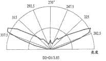
图16A和图16B图示当距离D2等于D1/3时发光器件封装的亮度分布和观察图案,以及图17A和图17B图示当距离D2等于D1/3.85时发光器件封装的亮度分布和观察图案。 16A and 16B illustrate the luminance distribution and observation pattern of the light emitting device package when the distance D2 is equal to D1/3, and FIGS. 17A and 17B illustrate the luminance distribution and observation pattern of the light emitting device package when the distance D2 is equal to D1/3.85 . the
尽管当距离D2等于D1/3时的结果截然不同于上述距离D2等于D1/2.5的情况的结果,但可理解中心亮度随视角增大稍微增大。 Although the results when the distance D2 is equal to D1/3 are quite different from those of the above-mentioned case where the distance D2 is equal to D1/2.5, it can be understood that the center brightness slightly increases with the increase of the viewing angle. the
在下列表1中概括了最大发光强度角和中心发光强度根据距离D2的变化的变化。 The variation of the maximum luminous intensity angle and the central luminous intensity as a function of the variation of the distance D2 is summarized in Table 1 below. the
表1 Table 1
最大发光强度角越大,呈现出亮度均匀性的区域就越大。中心发光强度必须在15%到45%范围内,以防止热点或者暗区。 The larger the angle of maximum luminous intensity, the larger the area exhibiting brightness uniformity. The center glow intensity must be in the range of 15% to 45% to prevent hot spots or dark areas. the
如表1中所述,等于D1/2.5的距离D2造成最大发光强度角过窄,而等于D1/7的距离D2造成中心发光强度很高。 As stated in Table 1, a distance D2 equal to D1/2.5 results in a too narrow maximum luminous intensity angle, while a distance D2 equal to D1/7 results in a high central luminous intensity. the
基于以上结果,假定透镜30的直径是D1以及从LED芯片40到透镜30的中心凹陷的距离是D2,当D2在如以下等式3表示的范围内时可以得到符合本发明的设计意图的最佳背光单元。 Based on the above results, assuming that the diameter of the
[等式3] [equation 3]
Dl/7<D2<DL/2.4 Dl/7<D2<DL/2.4
可理解,作为在改变距离D2的同时检查亮度分布和观察图案的结果,当距离D2等于D1/3.85时,如图17A中所示能够实现增强的亮度均匀性。 It can be understood that, as a result of examining the luminance distribution and observing patterns while changing the distance D2, when the distance D2 is equal to D1/3.85, enhanced luminance uniformity can be achieved as shown in FIG. 17A. the
然而,考虑到发光器件封装、LCD板等上存在背光单元的各种组成薄膜,距离D2的上述范围能够为获得的背光单元提供更好的结果。 However, the above-mentioned range of the distance D2 can provide better results for the obtained backlight unit in consideration of the presence of various constituent films of the backlight unit on the light emitting device package, LCD panel, and the like. the
<曲率半径的确定> <Determination of radius of curvature>
透镜30的凹陷附近的曲面的曲率半径是调整视角的最大发光强度角的要素。 The radius of curvature of the curved surface near the concave of the
如果曲率半径过大,则如图18A中所示,视角的最大发光强度角变窄。另一方面,如果曲率半径过小,则如图18B中所示,视角的最大发光强度角变宽,但这同时导致距离D2减小,从而可能在中心造成热点。 If the radius of curvature is too large, the maximum luminous intensity angle of the viewing angle becomes narrow as shown in FIG. 18A . On the other hand, if the radius of curvature is too small, as shown in FIG. 18B , the angle of maximum luminous intensity of the viewing angle becomes wider, but this simultaneously causes the distance D2 to decrease, possibly causing a hot spot at the center. the
接着,将不完全地描述发光器件封装随距离D2的变化的亮度分布和观察图案。 Next, the luminance distribution and observation pattern of the light emitting device package as a function of the distance D2 will be described incompletely. the
图19A和图19B是图示当曲率半径R是1.8mm时发光器件封装的亮度分布和观察图案的视图。 19A and 19B are views illustrating the luminance distribution and observation pattern of the light emitting device package when the radius of curvature R is 1.8 mm. the
图20A和图20B是图示当曲率半径R是0.8mm时发光器件封装的亮度分布和观察图案的视图。 20A and 20B are views illustrating the luminance distribution and observation pattern of the light emitting device package when the radius of curvature R is 0.8 mm. the
如从以上描述中可理解到的,当曲率半径R具有约为1.8mm的相对大的值时,如图19B中所示视角的最大发光强度角减小到约250°到290°的范围。 As can be understood from the above description, when the radius of curvature R has a relatively large value of about 1.8 mm, the maximum luminous intensity angle of the viewing angle as shown in FIG. 19B is reduced to a range of about 250° to 290°. the
另一方面,当曲率半径R具有约为0.8mm的相对小的值时,如图20B中所示,视角的最大发光强度角增大到约337°到202°的范围,但这同时导致距离D2减小,从而可能在中心造成热点。 On the other hand, when the radius of curvature R has a relatively small value of about 0.8mm, as shown in FIG. D2 decreases, possibly causing a hot spot in the center. the
图21A和图21B是图示当曲率半径R是1.0mm时发光器件封装的亮度分布和观察图案的视图,以及图22A和图22B是图示当曲率半径R是1.6mm时发光器件封装的亮度分布和观察图案的视图。 21A and 21B are views illustrating the luminance distribution and observation pattern of the light emitting device package when the radius of curvature R is 1.0 mm, and FIGS. 22A and 22B are views illustrating the luminance of the light emitting device package when the radius of curvature R is 1.6 mm. Views of the distribution and observation patterns. the
可理解,1.0mm的曲率半径R产生与0.8mm的曲率半径R大致相同的亮度分布。 It can be appreciated that a radius of curvature R of 1.0 mm produces substantially the same luminance distribution as a radius of curvature R of 0.8 mm. the
在下列表2中概括了最大发光强度角和中心发光强度根据曲率半径 R的变化的变化。 The variation of the maximum luminous intensity angle and central luminous intensity as a function of the radius of curvature R is summarized in Table 2 below. the
表2 Table 2
如表2中所述,小于0.8mm的曲率半径R造成视角很窄,而大于0.8mm的曲率半径R在中心造成热点。 As described in Table 2, a radius of curvature R of less than 0.8 mm causes a narrow viewing angle, while a radius of curvature R of greater than 0.8 mm causes a hot spot in the center. the
应注意,表2表示基于统一的透镜直径的数值,因为曲率半径与透镜直径有关,因此当透镜直径改变时这些数值可能改变。 It should be noted that Table 2 represents values based on a uniform lens diameter, since the radius of curvature is related to the lens diameter, and therefore these values may change when the lens diameter changes. the
[等式4] [equation 4]
0.8mm<R<1.8mm 0.8mm<R<1.8mm
可理解,作为在改变曲率半径R的同时检查亮度分布和观察图案的结果,当曲率半径R是1.6mm时,如图22A中所示能够实现增强的亮度均匀性。 It can be understood that, as a result of examining the luminance distribution and observing patterns while changing the radius of curvature R, when the radius of curvature R is 1.6 mm, enhanced luminance uniformity can be achieved as shown in FIG. 22A . the
透镜30的曲率半径可以基于位置改变,且这样的透镜被称为非球面透镜。应注意,即使在非球面透镜的情况下,整个曲率半径也必须在等式4的范围内而无论非球面系数如何。 The radius of curvature of the
透镜30可以具有一个或者多个曲率半径。
<透镜中心凹陷角的确定> <Determination of lens concave angle>
透镜30的中心凹陷角用θ表示。凹陷可以以直线成形,或者可以以预定的曲率半径成形。 The central concavity angle of the
透镜30的中心凹陷用于均匀地折射、透射或者反射光,以及因此能够根据凹陷角来控制光的折射率、透射率和反射率。 The center of the
如图23A中所示,当中心凹陷角度宽时,光可能聚集在中心而不是均匀地散射。另一方面,当如图23B中所示中心凹陷角度窄时,光大多 数被散射到周围从而可能在中心造成暗区。 As shown in FIG. 23A, when the center depression angle is wide, light may gather at the center instead of being scattered uniformly. On the other hand, when the central depression angle is narrow as shown in FIG. 23B, light is mostly scattered to the surroundings to possibly cause a dark area at the center. the
图24A和图24B是图示当角θ是90°时发光器件封装的亮度分布和观察图案的视图。 24A and 24B are views illustrating the luminance distribution and observation pattern of the light emitting device package when the angle θ is 90°. the
另外,图25A和图25B是图示当角θ是120°时发光器件封装的亮度分布和观察图案的视图。 In addition, FIGS. 25A and 25B are views illustrating the luminance distribution and observation pattern of the light emitting device package when the angle θ is 120°. the
如从以上描述中可理解到的,当角θ具有90°的相对小的值时,如图24A中所示光被散射到周围,从而由于亮度差在中心出现带状图案。 As can be understood from the above description, when the angle θ has a relatively small value of 90°, light is scattered around as shown in FIG. 24A so that a band pattern appears at the center due to brightness difference. the
当角θ具有120°的相对大的值时,如图25B中所示,光聚集在中心,从而阻止观察图案平缓变化,结果如图25A中所示在中心造成热点。 When the angle θ has a relatively large value of 120°, as shown in FIG. 25B , light gathers at the center, preventing the observation pattern from changing smoothly, resulting in a hot spot at the center as shown in FIG. 25A . the
图26A和图26B是图示当角θ是100°时发光器件封装的亮度分布和观察图案的视图,以及图27A和图27B是图示当角θ是110°时发光器件封装的亮度分布和观察图案的视图。 26A and 26B are views illustrating the luminance distribution and observation pattern of the light emitting device package when the angle θ is 100°, and FIGS. 27A and 27B are views illustrating the luminance distribution and the observation pattern of the light emitting device package when the angle θ is 110°. Observe the view of the pattern. the
可理解,100°的角θ产生与110°的角θ大致相同的亮度分布,并在中心实现亮度均匀性。 It can be appreciated that an angle θ of 100° produces approximately the same luminance distribution as an angle θ of 110° and achieves luminance uniformity at the center. the
在下列表3中概括了最大发光强度角和中心发光强度根据中心凹陷角的变化的变化。 The variation of the maximum luminous intensity angle and the central luminous intensity as a function of the central concave angle is summarized in Table 3 below. the
表3 table 3
参照图28,当透镜的中心凹陷具有最佳角度时,从LED芯片40发出的光束被透镜30的邻近外表面折射从而抵达特定平面时产生的光通量之间的距离d1和d2可能彼此相等。基于相等的光通量距离,能够在0°到45°的视角附近(即在背光单元上的LED封装的上方)实现亮度均匀性。 Referring to FIG. 28 , when the central depression of the lens has an optimal angle, the distances d1 and d2 between the luminous fluxes generated when the light beam emitted from the
透镜30的中心凹陷角可以根据透镜30的大小和高度而改变。考虑到上述结果,当中心凹陷角在由下列等式5限定的范围内时能够实现最理想的亮度均匀性。 The central depression angle of the
[等式5] [equation 5]
90°<θ<120° 90°<θ<120°
当中心凹陷具有弯曲轮廓时,在由如图28中所示用直线表示的该弯曲轮廓的切线限定的角在等式5的范围内时能够实现理想的亮度均匀性。 When the central depression has a curved profile, ideal luminance uniformity can be achieved when the angle defined by the tangent to the curved profile represented by a straight line as shown in FIG. 28 is within the range of Equation 5. the
因此,当发光器件封装使用透镜30以满足等式3到等式5中至少之一时,使用该发光器件封装制造的背光单元能够实现充分的亮度均匀性。 Therefore, when the light emitting device package satisfies at least one of Equation 3 to Equation 5 using the
使用呈现出上述理想的亮度均匀性的透镜的背光单元能够使相邻的发光器件封装之间的距离增大超过一倍,由此能够减少发光器件封装的数量,并且还能够极大地减小背光单元的厚度。 A backlight unit using a lens exhibiting the above-mentioned ideal brightness uniformity can more than double the distance between adjacent light emitting device packages, whereby the number of light emitting device packages can be reduced, and also the backlight can be greatly reduced. The thickness of the element. the
另外,按本发明中所提出的制造的背光单元在LED局部变暗时在块之间不产生边界。也就是说,发光器件封装的广视角能够消除作为使用LED的背光单元的基本性能品质的在局部变暗时块的边界可见的问题。结果,能够在使用局部变暗的情况下在实现增强的对比度,同时最小化电耗,并且能够从屏幕质量的角度提供最理想的LED背光配置。 In addition, a backlight unit fabricated as proposed in the present invention does not produce borders between blocks when the LEDs are locally dimmed. That is, the wide viewing angle of the light emitting device package can eliminate the problem that the boundaries of the blocks are visible when locally dimmed, which is an essential performance quality of a backlight unit using LEDs. As a result, enhanced contrast can be achieved while using local dimming while minimizing power consumption and providing the most ideal LED backlight configuration from a screen quality standpoint. the
图29图示满足上述要素的透镜30的示例形状。假定在LED芯片40上没有封装材料70,则透镜30可在其下表面上设置有要装配到安装槽中的突起30a。 FIG. 29 illustrates an example shape of the
如图30中所示,当透镜30直接形成在LED 40上或者附接到LED 40时,透镜30可以具有图29中所示的形状。 As shown in FIG. 30, when the
当在LED芯片40上设置作为保护层的封装材料70时,或者当设置封装材料70以制造能够变色为例如白色的发光器件封装并且将荧光体混合到封装材料70中时,可提供具有图31中所示的形状的透镜31。 When the
具体而言,透镜31可具有平坦的下表面,该平坦的下表面没有要装配到安装槽中的突起。 Specifically, the
图32图示一种实施方式,其中如上所述地设置多个LED芯片40。这多个LED芯片40可以发出相同颜色的光或者不同颜色的光。 Fig. 32 illustrates an embodiment in which a plurality of
在该实施方式中,从多个LED芯片40的中心点到中心凹陷的最低部分的距离D2和透镜的直径D1满足D2大于D1/7且小于D1/2.4的上述条件。在此情况下,如图所示,LED芯片40的中心点位于与LED芯片40的安装平面相同的平面内。 In this embodiment, the distance D2 from the center point of the plurality of
图33图示一种实施方式,其中设置多个LED芯片40,并且透镜32 具有多个凹陷。在此情况下,LED芯片40的数量可以等于凹陷的数量,并且从每个LED芯片40到对应的凹陷的最低部分的距离D2满足如等式3所示的上述条件。 Figure 33 illustrates an embodiment in which a plurality of
<液晶显示装置> <Liquid crystal display device>
如图34中所示,能够构建在使用包含上述透镜的发光器件封装的背光单元100上布置液晶板200的这样的液晶显示装置400。 As shown in FIG. 34 , such a liquid
背光单元100可以是直接型背光单元和光导板型背光单元中的任意之一。 The
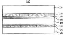
位于背光单元100上的液晶板200包括彼此对置的上衬底210和下衬底220,在上衬底210和下衬底220之间填充液晶层230(参见图35)。 The
可在液晶板200的一侧设置驱动单元(未示出)用于驱动液晶板200。 A driving unit (not shown) for driving the
可设置下覆层310以覆盖背光单元100,以及可在液晶板200的上侧设置上覆层320以覆盖液晶板200的整个表面。 A
液晶板200包含排列成矩阵的作为像素单元的液晶单元,并适合于通过根据从驱动单元传送的图像信号信息来调整液晶单元的光透射率以形成图像。 The
驱动单元可以包括柔性印刷电路(FPC)板、安装在FPC板一侧的驱动芯片、以及连接到FPC板的另一侧的印刷电路板(PCB)。 The driving unit may include a flexible printed circuit (FPC) board, a driving chip mounted on one side of the FPC board, and a printed circuit board (PCB) connected to the other side of the FPC board. the
如图所示,背光单元100位于液晶板200的背面,并且在背光单元100上可设置多个光学片110。 As shown in the figure, the
光学片110位于液晶板200的背表面,并且可包括散射片、棱镜片以及保护片。 The
在此,散射片用于使来自背光单元100的光散射以提供光给液晶板200。棱镜片被配置为使得在棱镜片的上表面上以预定间距布置三角棱柱形式的微棱镜。棱镜片用于将被散射片散射的光汇聚到与棱镜片上方的液晶板200垂直的方向上。在棱镜片上形成的微棱镜具有期望的有角的形状。几乎所有穿过棱镜片的光都垂直于棱镜片行进,从而提供亮度均匀性。作为最上层片的保护片用于保护容易被剐蹭到的棱镜片。 Here, the diffusion sheet serves to diffuse light from the
如图35中所示,液晶板200的下衬底210设置有:矩阵状的多个栅极线和多个数据线,以及位于栅极线和数据线的交叉处的像素电极和薄膜晶体管(TFT)240。 As shown in FIG. 35 , the
如果通过TFT 240施加的信号电压被像素电极提供给液晶层230,则液晶层230响应于信号电压而定向,从而光透射率被确定。 If a signal voltage applied through the
上衬底220设置有:由当透过光时表现特定颜色的RGB像素组成的滤色器270,以及由比如氧化铟锡(ITO)或者氧化铟锌(IZO)等透明导电材料制成的共用电极260。定向膜250可以设置在液晶层230的上侧和下侧。 The
上述液晶显示装置400可以通过使用上述背光单元100实现最大性能。 The liquid
<液晶显示电视机> <LCD TV>
通过使用上述液晶显示装置400,能够构建液晶显示电视机。 By using the liquid
如图36中所示,液晶显示电视机500可以包括调谐器510以接收广播数据流,以及包括处理器520、解码器530和A/V(音频/视频)输出单元540,广播数据流经过A/V输出单元被传送给液晶显示装置400以在液晶显示装置400上显示。 As shown in FIG. 36 , a liquid crystal
能够在通过控制器550的操作中控制调谐器510或者处理器520,并且控制器550可以设置有存储器560。 The
之后,如果用户选中和指定任意广播频道,则控制器550控制调谐器510和处理器520以调谐到相应的广播频道。处理器520分离并输出经过该广播频道提供的广播节目的音频和视频数据流。 Afterwards, if the user selects and designates any broadcast channel, the
解码器530将从处理器520输出的广播节目的数据流解码为音频和视频信息,以经过A/V输出单元450在例如液晶显示装置400、音频输出单元570(比如扬声器单元)等输出装置上输出音频和视频信息。 The
在此情况下,背光驱动装置410驱动背光单元100,由此允许在液晶板200上显示电视帧。 In this case, the
传送给处理器520的广播数据流可以经过互连网提供。 The broadcast data stream transmitted to the
对于本领域技术人员而言,显然在不偏离本发明的精神或范围的情况下可以在本发明中做出各种修改和变化。因而,本发明意在涵盖对所提供的发明方案的落在所附权利要求及其等同方案的范围内的修改和变化。 It will be apparent to those skilled in the art that various modifications and variations can be made in the present invention without departing from the spirit or scope of the inventions. Thus, it is intended that the present invention covers the modifications and variations of the presented inventive arrangements that come within the scope of the appended claims and their equivalents. the
Claims (17)
Applications Claiming Priority (3)
| Application Number | Priority Date | Filing Date | Title |
|---|---|---|---|
| KR1020080069651AKR100902908B1 (en) | 2008-07-17 | 2008-07-17 | Light emitting device package and backlight unit using same |
| KR10-2008-0069651 | 2008-07-17 | ||
| PCT/KR2008/006541WO2010008118A1 (en) | 2008-07-17 | 2008-11-06 | Light emitting device package, back-light unit, and liquid crystal display device using the same |
Publications (2)
| Publication Number | Publication Date |
|---|---|
| CN102099932A CN102099932A (en) | 2011-06-15 |
| CN102099932Btrue CN102099932B (en) | 2013-06-19 |
Family
ID=40982775
Family Applications (1)
| Application Number | Title | Priority Date | Filing Date |
|---|---|---|---|
| CN2008801303752AActiveCN102099932B (en) | 2008-07-17 | 2008-11-06 | Light emitting device package, back-light unit, and liquid crystal display device using the same |
Country Status (5)
| Country | Link |
|---|---|
| US (1) | US7909486B2 (en) |
| EP (1) | EP2301086B1 (en) |
| KR (1) | KR100902908B1 (en) |
| CN (1) | CN102099932B (en) |
| WO (1) | WO2010008118A1 (en) |
Families Citing this family (30)
| Publication number | Priority date | Publication date | Assignee | Title |
|---|---|---|---|---|
| TW200947057A (en)* | 2008-05-06 | 2009-11-16 | Advanced Optoelectronic Tech | Light module for LCD backlight module |
| KR101023960B1 (en) | 2008-12-01 | 2011-03-28 | 주식회사 루멘스 | Light emitting diode package |
| KR101670981B1 (en)* | 2009-03-31 | 2016-10-31 | 서울반도체 주식회사 | Tube type or channel type led lighting apparatus |
| US8348460B2 (en)* | 2009-05-01 | 2013-01-08 | Abl Ip Holding Llc | Lighting apparatus with several light units arranged in a heatsink |
| CN101937889A (en)* | 2009-06-29 | 2011-01-05 | 鸿富锦精密工业(深圳)有限公司 | Semiconductor element packaging structure and packaging method thereof |
| US20110038141A1 (en)* | 2009-08-11 | 2011-02-17 | Martin David Tillin | Lateral emission led backlight for lcd |
| FR2950182A1 (en)* | 2009-09-16 | 2011-03-18 | Thomson Licensing | IMAGE PROCESSING METHOD |
| TWI409975B (en) | 2009-12-01 | 2013-09-21 | Au Optronics Corp | Light source device with large illumination angle and manufacturing method thereof |
| US20110156092A1 (en)* | 2009-12-30 | 2011-06-30 | Lumenmax Optoelectronics Co., Ltd. | Smt encapsulation body of a light-emitting diode with a wide-angle illumination light shape |
| KR101646262B1 (en)* | 2010-03-25 | 2016-08-12 | 엘지이노텍 주식회사 | Light emitting device package and light unit having the seme |
| KR101701453B1 (en)* | 2010-06-11 | 2017-02-03 | 서울반도체 주식회사 | Light emitting diode package |
| US10024510B2 (en)* | 2010-10-26 | 2018-07-17 | Steven G. Hammond | Flexible light emitting diode lighting process and assembly |
| CN102655198B (en)* | 2011-03-03 | 2015-09-23 | 展晶科技(深圳)有限公司 | LED source |
| US20120236532A1 (en)* | 2011-03-14 | 2012-09-20 | Koo Won-Hoe | Led engine for illumination |
| KR101957184B1 (en) | 2011-12-02 | 2019-03-13 | 엘지전자 주식회사 | Backlight unit and display apparatus having the same |
| US20130126922A1 (en)* | 2011-11-21 | 2013-05-23 | Foxsemicon Integrated Technology, Inc. | Light emitting diode incorporating light converting material |
| US8921872B2 (en)* | 2011-12-09 | 2014-12-30 | Sony Corporation | Display unit and method of manufacturing the same, electronic apparatus, illumination unit, and light-emitting device and method of manufacturing the same |
| EP2645434A1 (en)* | 2012-03-30 | 2013-10-02 | Lumenmax Optoelectronics Co., Ltd. | Led-packaging arrangement with uniform light and wide angle |
| KR101417258B1 (en) | 2012-04-05 | 2014-07-08 | 엘지이노텍 주식회사 | Member for controlling luminous flux and display device having the same |
| TWI529969B (en)* | 2013-09-11 | 2016-04-11 | 新世紀光電股份有限公司 | Light emitting diode package structure |
| TW201604625A (en)* | 2014-07-17 | 2016-02-01 | 李政道 | Backlight device |
| WO2016057302A1 (en) | 2014-10-06 | 2016-04-14 | Edgewell Personal Care Brands, Llc | Method of shaping a surface coating on a razor blade using centrifugal force |
| KR102277127B1 (en) | 2014-10-17 | 2021-07-15 | 삼성전자주식회사 | Light emitting device package |
| TWI532222B (en)* | 2015-04-21 | 2016-05-01 | 隆達電子股份有限公司 | Light emitting device and lens structure thereof |
| US10851967B2 (en) | 2017-11-17 | 2020-12-01 | Osram Gmbh | Lens, corresponding lighting device, lighting installation and method |
| CN108281537A (en)* | 2018-03-20 | 2018-07-13 | 木林森股份有限公司 | Packaging structure of L ED lamp pearl |
| CN109212831B (en)* | 2018-10-23 | 2021-08-17 | 厦门天马微电子有限公司 | Backlight module and display device |
| KR102341997B1 (en)* | 2019-11-28 | 2021-12-22 | 엘지전자 주식회사 | Car lamp using semiconductor light emitting device |
| CN111223981A (en)* | 2020-03-12 | 2020-06-02 | 宁波升谱光电股份有限公司 | A UV LED device |
| JP7007606B2 (en)* | 2020-04-15 | 2022-01-24 | 日亜化学工業株式会社 | Light emitting device and its manufacturing method |
Citations (5)
| Publication number | Priority date | Publication date | Assignee | Title |
|---|---|---|---|---|
| KR20060040505A (en)* | 2004-11-06 | 2006-05-10 | 삼성전자주식회사 | Apparatus and method for outputting data according to options set by caller |
| CN2788226Y (en)* | 2005-06-01 | 2006-06-14 | 巨虹电子股份有限公司 | LCD Backlight Optical Components |
| WO2007021149A1 (en)* | 2005-08-19 | 2007-02-22 | Lg Chem, Ltd. | Side emitting lens, light emitting device using the side emitting lens, mold assembly for preparing the side emitting lens and method for preparing the side emitting lens |
| JP2007140524A (en)* | 2005-11-15 | 2007-06-07 | Samsung Electro Mech Co Ltd | Lens for uniform light distribution and light emitting device using the same |
| KR20080038669A (en)* | 2006-10-30 | 2008-05-07 | 삼성전자주식회사 | Side-emitting lens, backlight unit and liquid crystal display device having same |
Family Cites Families (12)
| Publication number | Priority date | Publication date | Assignee | Title |
|---|---|---|---|---|
| KR100586965B1 (en)* | 2004-05-27 | 2006-06-08 | 삼성전기주식회사 | Light emitting diode elements |
| KR100586968B1 (en)* | 2004-05-28 | 2006-06-08 | 삼성전기주식회사 | LED Package and Backlight Assembly for LCD |
| US7748873B2 (en)* | 2004-10-07 | 2010-07-06 | Seoul Semiconductor Co., Ltd. | Side illumination lens and luminescent device using the same |
| KR101080355B1 (en)* | 2004-10-18 | 2011-11-04 | 삼성전자주식회사 | Light emitting diode, lens for the same |
| KR20060040502A (en)* | 2004-11-06 | 2006-05-10 | 럭스피아 주식회사 | Light emitting unit and backlight device employing the same |
| TWI261654B (en)* | 2004-12-29 | 2006-09-11 | Ind Tech Res Inst | Lens and LED with uniform light emitted applying the lens |
| KR100691179B1 (en)* | 2005-06-01 | 2007-03-09 | 삼성전기주식회사 | Side emitting type LED package and manufacturing method thereof |
| KR100788426B1 (en)* | 2005-11-19 | 2007-12-24 | 삼성전자주식회사 | Backlight unit and liquid crystal display including the same |
| US7775687B2 (en)* | 2006-02-20 | 2010-08-17 | Nichia Corporation | Light emitting device |
| TWI319629B (en)* | 2006-06-27 | 2010-01-11 | Au Optronics Corp | Light emitting diode module |
| JP2008010693A (en)* | 2006-06-30 | 2008-01-17 | Hitachi Displays Ltd | Liquid crystal display |
| TWM352000U (en)* | 2008-09-19 | 2009-03-01 | Genius Electronic Optical Co Ltd | Optic lens emitting light from both lateral sides |
- 2008
- 2008-07-17KRKR1020080069651Apatent/KR100902908B1/enactiveActive
- 2008-11-06WOPCT/KR2008/006541patent/WO2010008118A1/enactiveApplication Filing
- 2008-11-06CNCN2008801303752Apatent/CN102099932B/enactiveActive
- 2008-11-06EPEP08876586.2Apatent/EP2301086B1/enactiveActive
- 2008-11-18USUS12/273,401patent/US7909486B2/enactiveActive
Patent Citations (5)
| Publication number | Priority date | Publication date | Assignee | Title |
|---|---|---|---|---|
| KR20060040505A (en)* | 2004-11-06 | 2006-05-10 | 삼성전자주식회사 | Apparatus and method for outputting data according to options set by caller |
| CN2788226Y (en)* | 2005-06-01 | 2006-06-14 | 巨虹电子股份有限公司 | LCD Backlight Optical Components |
| WO2007021149A1 (en)* | 2005-08-19 | 2007-02-22 | Lg Chem, Ltd. | Side emitting lens, light emitting device using the side emitting lens, mold assembly for preparing the side emitting lens and method for preparing the side emitting lens |
| JP2007140524A (en)* | 2005-11-15 | 2007-06-07 | Samsung Electro Mech Co Ltd | Lens for uniform light distribution and light emitting device using the same |
| KR20080038669A (en)* | 2006-10-30 | 2008-05-07 | 삼성전자주식회사 | Side-emitting lens, backlight unit and liquid crystal display device having same |
Also Published As
| Publication number | Publication date |
|---|---|
| US7909486B2 (en) | 2011-03-22 |
| EP2301086A1 (en) | 2011-03-30 |
| EP2301086B1 (en) | 2018-01-03 |
| CN102099932A (en) | 2011-06-15 |
| US20100014281A1 (en) | 2010-01-21 |
| WO2010008118A1 (en) | 2010-01-21 |
| EP2301086A4 (en) | 2014-06-11 |
| KR100902908B1 (en) | 2009-06-15 |
Similar Documents
| Publication | Publication Date | Title |
|---|---|---|
| CN102099932B (en) | Light emitting device package, back-light unit, and liquid crystal display device using the same | |
| US11579487B2 (en) | Backlight unit and display device including backlight unit | |
| US8696175B2 (en) | Light emitting diode and lens for the same | |
| US8985798B2 (en) | Backlight unit and display apparatus using the same | |
| JP5066572B2 (en) | Backlight unit and liquid crystal display device including the same | |
| US8704964B2 (en) | Liquid crystal display device | |
| US20110051046A1 (en) | Optical sheet, backlight unit and liquid crystal display device having the same and method of fabricating optical sheet | |
| US10203549B2 (en) | Backlight unit and display device including backlight unit | |
| US20100283936A1 (en) | Liquid crystal display device including LED light source | |
| KR101554611B1 (en) | A light scattering lens and light source package | |
| KR20120057726A (en) | Liquid crystal display device | |
| KR101597574B1 (en) | LED backlight unit and liquid crystal display using the same | |
| US20180239079A1 (en) | Backlight unit and liquid crystal display device including the same | |
| US20130013252A1 (en) | Light-emitting device, display apparatus, and method for designing reflective member | |
| KR20120118565A (en) | Light emitting diode package and liquid crystal display device having the same | |
| US20070081355A1 (en) | Light generating unit, display device having the same, and method thereof | |
| KR101602960B1 (en) | Back light unit and liquid crystal display device having the same | |
| KR101943958B1 (en) | Light emitting package and backlight unit having the same | |
| KR101774572B1 (en) | Display device | |
| EP2354837A1 (en) | Image display apparatus and method of manufacturing the same | |
| KR20110042251A (en) | Backlight Device and Backlight Light Source | |
| KR20160063459A (en) | Light emitting diode array and backlight unit having the same |
Legal Events
| Date | Code | Title | Description |
|---|---|---|---|
| C06 | Publication | ||
| PB01 | Publication | ||
| C10 | Entry into substantive examination | ||
| SE01 | Entry into force of request for substantive examination | ||
| C14 | Grant of patent or utility model | ||
| GR01 | Patent grant |