CN102097561A - Semi-conductor light emitting device and method for manufacturing thereof - Google Patents
Semi-conductor light emitting device and method for manufacturing thereofDownload PDFInfo
- Publication number
- CN102097561A CN102097561ACN2010101851239ACN201010185123ACN102097561ACN 102097561 ACN102097561 ACN 102097561ACN 2010101851239 ACN2010101851239 ACN 2010101851239ACN 201010185123 ACN201010185123 ACN 201010185123ACN 102097561 ACN102097561 ACN 102097561A
- Authority
- CN
- China
- Prior art keywords
- semiconductor layer
- protuberance
- substrate
- layer
- semiconductor light
- Prior art date
- Legal status (The legal status is an assumption and is not a legal conclusion. Google has not performed a legal analysis and makes no representation as to the accuracy of the status listed.)
- Granted
Links
Images


Classifications
- H—ELECTRICITY
- H10—SEMICONDUCTOR DEVICES; ELECTRIC SOLID-STATE DEVICES NOT OTHERWISE PROVIDED FOR
- H10H—INORGANIC LIGHT-EMITTING SEMICONDUCTOR DEVICES HAVING POTENTIAL BARRIERS
- H10H20/00—Individual inorganic light-emitting semiconductor devices having potential barriers, e.g. light-emitting diodes [LED]
- H10H20/80—Constructional details
- H10H20/81—Bodies
- H10H20/814—Bodies having reflecting means, e.g. semiconductor Bragg reflectors
- H—ELECTRICITY
- H10—SEMICONDUCTOR DEVICES; ELECTRIC SOLID-STATE DEVICES NOT OTHERWISE PROVIDED FOR
- H10H—INORGANIC LIGHT-EMITTING SEMICONDUCTOR DEVICES HAVING POTENTIAL BARRIERS
- H10H20/00—Individual inorganic light-emitting semiconductor devices having potential barriers, e.g. light-emitting diodes [LED]
- H10H20/80—Constructional details
- H10H20/81—Bodies
- H10H20/819—Bodies characterised by their shape, e.g. curved or truncated substrates
- H10H20/82—Roughened surfaces, e.g. at the interface between epitaxial layers
- H—ELECTRICITY
- H10—SEMICONDUCTOR DEVICES; ELECTRIC SOLID-STATE DEVICES NOT OTHERWISE PROVIDED FOR
- H10H—INORGANIC LIGHT-EMITTING SEMICONDUCTOR DEVICES HAVING POTENTIAL BARRIERS
- H10H20/00—Individual inorganic light-emitting semiconductor devices having potential barriers, e.g. light-emitting diodes [LED]
- H10H20/80—Constructional details
- H10H20/81—Bodies
- H10H20/815—Bodies having stress relaxation structures, e.g. buffer layers
- H—ELECTRICITY
- H10—SEMICONDUCTOR DEVICES; ELECTRIC SOLID-STATE DEVICES NOT OTHERWISE PROVIDED FOR
- H10H—INORGANIC LIGHT-EMITTING SEMICONDUCTOR DEVICES HAVING POTENTIAL BARRIERS
- H10H20/00—Individual inorganic light-emitting semiconductor devices having potential barriers, e.g. light-emitting diodes [LED]
- H10H20/80—Constructional details
- H10H20/81—Bodies
- H10H20/819—Bodies characterised by their shape, e.g. curved or truncated substrates
- H—ELECTRICITY
- H10—SEMICONDUCTOR DEVICES; ELECTRIC SOLID-STATE DEVICES NOT OTHERWISE PROVIDED FOR
- H10H—INORGANIC LIGHT-EMITTING SEMICONDUCTOR DEVICES HAVING POTENTIAL BARRIERS
- H10H20/00—Individual inorganic light-emitting semiconductor devices having potential barriers, e.g. light-emitting diodes [LED]
- H10H20/01—Manufacture or treatment
- H10H20/011—Manufacture or treatment of bodies, e.g. forming semiconductor layers
- H10H20/013—Manufacture or treatment of bodies, e.g. forming semiconductor layers having light-emitting regions comprising only Group III-V materials
- H10H20/0133—Manufacture or treatment of bodies, e.g. forming semiconductor layers having light-emitting regions comprising only Group III-V materials with a substrate not being Group III-V materials
- H10H20/01335—Manufacture or treatment of bodies, e.g. forming semiconductor layers having light-emitting regions comprising only Group III-V materials with a substrate not being Group III-V materials the light-emitting regions comprising nitride materials
Landscapes
- Led Devices (AREA)
Abstract
Description
Translated fromChinese技术领域technical field
本发明涉及半导体设备,更具体地说,涉及氮化物半导体发光设备。The present invention relates to semiconductor devices, and more particularly, to nitride semiconductor light emitting devices.
背景技术Background technique
本申请要求2009年12月11日提交的韩国专利申请No.10-2009-0122914的优先权,此处以引证的方式并入其内容,就像在此进行了完整阐述一样。This application claims priority from Korean Patent Application No. 10-2009-0122914 filed on December 11, 2009, the contents of which are hereby incorporated by reference as if fully set forth herein.
氮化物半导体发光设备包括紫外线、蓝色和绿色发光区域。特别是,基于GaN的氮化物半导体发光设备可以应用于红/绿发光二极管(LED)的光学设备以及与MESFET(金属半导体场效应晶体管)或者HEMT(异质结型场效应晶体管)的高速开关或高功率设备相对应的电子设备。Nitride semiconductor light emitting devices include ultraviolet, blue and green light emitting regions. In particular, GaN-based nitride semiconductor light-emitting devices can be applied to optical devices of red/green light-emitting diodes (LEDs) and high-speed switches or Electronic equipment corresponding to high-power equipment.
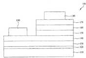
图1是例示了根据相关技术的氮化物半导体发光设备的截面图。FIG. 1 is a cross-sectional view illustrating a nitride semiconductor light emitting device according to the related art.
如图1所示,根据相关技术的氮化物半导体发光设备包括基板110、缓冲层120、未掺杂半导体层130、N型氮化物半导体层140、有源层150、P型氮化物半导体层160、透明电极层170、位于透明电极层170上的P型电极180、以及位于N型氮化物半导体层140上的通过蚀刻有源层150和P型氮化物半导体层160的预定部分而露出的N型电极190。As shown in FIG. 1 , a nitride semiconductor light emitting device according to the related art includes a
当向半导体发光设备100中的P型电极180和N型电极190施加电压时,会在P型氮化物半导体层160和N型氮化物半导体层140之间施加正向偏压,由此电子和空穴在有源层150中复合,从而发光。When a voltage is applied to the P-
氮化物半导体发光设备中的一个重要问题是如何有效地将有源层150中产生的光导出到外部。在根据相关技术的氮化物半导体发光设备的情况下,如图2A所示,氮化物半导体发光设备的构成材料的折射率大于氮化物半导体发光设备附近的周围材料(例如,空气、树脂、基板等)的折射率。因此,在氮化物半导体发光设备内部生成的光子发生全反射,然后被再次吸收到氮化物半导体发光设备的内部而没有从氮化物半导体发光设备射出,由此降低了光出射效率。An important issue in a nitride semiconductor light emitting device is how to efficiently guide light generated in the
为了克服这个问题,提出了一种在根据相关技术的半导体发光设备中以预定角度形成层叠结构的方法,由此导出有源层150中生成的一部分横向光。然而,该方法造成复杂的半导体发光设备的制造工艺,并且增加了制造成本。In order to overcome this problem, there is proposed a method of forming a stacked structure at a predetermined angle in a semiconductor light emitting device according to the related art, thereby deriving a part of lateral light generated in the
此外,根据相关技术的半导体发光设备的问题在于基板上生长的基于氮化物的半导体层的位错密度由于基板和基板上生长的基于氮化物的半导体层之间的晶格常数差所导致的应力而增加。In addition, a problem with the semiconductor light emitting device according to the related art is that the dislocation density of the nitride-based semiconductor layer grown on the substrate is stressed due to the lattice constant difference between the substrate and the nitride-based semiconductor layer grown on the substrate. And increase.
发明内容Contents of the invention
因此,本发明涉及一种半导体发光设备和制造该发光设备的方法,其能够基本上克服因相关技术的局限和缺点带来的一个或更多个问题。Accordingly, the present invention is directed to a semiconductor light emitting device and method of manufacturing the same that substantially overcome one or more problems due to limitations and disadvantages of the related art.
本发明的一个优点是提供了一种半导体发光设备和制造该发光设备的方法,其通过在基板的用于在其上生长氮化物半导体材料的表面上形成多个凸部来提高光出射效率。An advantage of the present invention is to provide a semiconductor light emitting device and a method of manufacturing the same, which improve light extraction efficiency by forming a plurality of protrusions on a surface of a substrate on which a nitride semiconductor material is grown.
本发明的另一个优点是提供了一种半导体发光设备和制造该发光设备的方法,其通过在各凸部上形成凹部来提高基板上生长的半导体层的质量,其中,所述凹部能够使得平坦地露出基板的表面或者凸部的内表面。Another advantage of the present invention is to provide a semiconductor light emitting device and a method of manufacturing the same, which improve the quality of a semiconductor layer grown on a substrate by forming a concave portion on each convex portion, wherein the concave portion enables flat The surface of the substrate or the inner surface of the protrusion is exposed to a large extent.
本发明的附加优点和特征将在下面的描述中部分描述且将对于本领域普通技术人员在研究下文后变得明显,或可以通过本发明的实践来了解。通过书面的说明书及其权利要求以及附图中特别指出的结构可以实现和获得本发明的目的和其它优点。Additional advantages and features of the invention will be set forth in part in the description which follows and will become apparent to those of ordinary skill in the art upon study of the following text, or may be learned by practice of the invention. The objectives and other advantages of the invention may be realized and attained by the structure particularly pointed out in the written description and claims hereof as well as the appended drawings.
为了实现这些和其它优点,按照本发明的目的,作为具体和广义的描述,提供了一种半导体发光设备,该半导体发光设备包括:基板;位于所述基板上的一个或更多个第一凸部,各第一凸部具有凹部,所述基板的表面通过该凹部平坦地露出;位于包括所述第一凸部的基板上的第一半导体层;位于所述第一半导体层上的有源层;位于所述有源层上的第二半导体层;位于所述第一半导体层的预定部分上的第一电极,其中,所述有源层和第二半导体层未形成在所述第一半导体层的所述预定部分上;以及位于所述第二半导体层上的第二电极。To achieve these and other advantages, and in accordance with the purpose of the present invention, as specifically and broadly described, there is provided a semiconductor light emitting device comprising: a substrate; one or more first protrusions on said substrate; Each first protrusion has a recess through which the surface of the substrate is flatly exposed; the first semiconductor layer on the substrate including the first protrusion; the active active layer on the first semiconductor layer layer; a second semiconductor layer on the active layer; a first electrode on a predetermined portion of the first semiconductor layer, wherein the active layer and the second semiconductor layer are not formed on the first on the predetermined portion of the semiconductor layer; and a second electrode on the second semiconductor layer.
在另一方面,提供了一种制造半导体发光设备的方法,该方法包括以下步骤:在基板上形成一个或更多个第一凸部,各第一凸部具有凹部,所述基板的表面通过该凹部平坦地露出;在包括所述第一凸部的基板上形成第一半导体层;在所述第一半导体层上形成有源层;在所述有源层上形成第二半导体层;对所述有源层的预定部分和第二半导体层的预定部分进行蚀刻直到所述第一半导体层被露出为止;以及在所述第一半导体层的预定部分上形成第一电极,其中,所述有源层和第二半导体层未形成在所述第一半导体层的所述预定部分上,并且在所述第二半导体层上形成第二电极。In another aspect, there is provided a method of manufacturing a semiconductor light emitting device, the method comprising the steps of: forming one or more first protrusions on a substrate, each first protrusion having a recess, the surface of the substrate passing The concave portion is exposed flatly; a first semiconductor layer is formed on the substrate including the first convex portion; an active layer is formed on the first semiconductor layer; a second semiconductor layer is formed on the active layer; A predetermined portion of the active layer and a predetermined portion of the second semiconductor layer are etched until the first semiconductor layer is exposed; and a first electrode is formed on the predetermined portion of the first semiconductor layer, wherein the An active layer and a second semiconductor layer are not formed on the predetermined portion of the first semiconductor layer, and a second electrode is formed on the second semiconductor layer.
应当理解,本发明的上述一般描述和下述详细描述是示例性和说明性的,且旨在提供所要求保护的本发明的进一步解释。It is to be understood that both the foregoing general description and the following detailed description of the present invention are exemplary and explanatory and are intended to provide further explanation of the invention as claimed.
附图说明Description of drawings
附图被包括在本申请中以提供对本发明的进一步理解,并结合到本申请中且构成本申请的一部分,附图示出了本发明的实施方式,且与说明书一起用于解释本发明的原理。附图中:The accompanying drawings, which are included to provide a further understanding of the invention and are incorporated in and constitute a part of this application, illustrate embodiments of the invention and together with the description serve to explain the invention. principle. In the attached picture:
图1是例示了根据相关技术的半导体发光设备的结构的截面图;1 is a cross-sectional view illustrating the structure of a semiconductor light emitting device according to the related art;
图2A例示了在根据相关技术的半导体发光设备中的全反射光;FIG. 2A illustrates total reflection light in a semiconductor light emitting device according to the related art;
图2B例示了根据相关技术的半导体发光设备中生成的位错;FIG. 2B illustrates dislocations generated in a semiconductor light emitting device according to the related art;
图3A是例示了根据本发明的第一实施方式的半导体发光设备的截面图;3A is a cross-sectional view illustrating a semiconductor light emitting device according to a first embodiment of the present invention;
图3B是例示了根据本发明的第一实施方式的其上形成有凸部的基板的立体图;3B is a perspective view illustrating a substrate on which protrusions are formed according to a first embodiment of the present invention;
图4A到图4C是例示了各凸部中的各种深度的凹部的截面图;4A to 4C are cross-sectional views illustrating recesses of various depths in each protrusion;
图5A和图5B是例示了各种形状的凸部的截面图;5A and 5B are cross-sectional views illustrating protrusions of various shapes;
图6A到6E是例示了根据本发明的第一实施方式的半导体发光设备的制造方法的截面图;6A to 6E are cross-sectional views illustrating a method of manufacturing a semiconductor light emitting device according to a first embodiment of the present invention;
图7是通过将相关技术的半导体发光设备中的内量子效率(IQE)与根据本发明的第一实施方式的半导体发光设备中的IQE进行比较,示出了根据本发明的第一实施方式的半导体发光设备中的IQE的提高的图;FIG. 7 is a graph showing the internal quantum efficiency (IQE) according to the first embodiment of the present invention by comparing the internal quantum efficiency (IQE) in the semiconductor light emitting device of the related art with the IQE in the semiconductor light emitting device according to the first embodiment of the present invention. A graph of the enhancement of IQE in semiconductor light emitting devices;
图8是通过将相关技术的半导体发光设备中的光出射效率与根据本发明的第一实施方式的半导体发光设备中的光出射效率进行比较,示出了根据本发明的第一实施方式的半导体发光设备中的光出射效率的提高的表;FIG. 8 is a graph showing the semiconductor light emission efficiency according to the first embodiment of the present invention by comparing the light emission efficiency in the semiconductor light emitting device of the related art with the light emission efficiency in the semiconductor light emitting device according to the first embodiment of the present invention. Table of enhancement of light extraction efficiency in a light emitting device;
图9是例示了根据本发明的第二实施方式的半导体发光设备的截面图;以及9 is a cross-sectional view illustrating a semiconductor light emitting device according to a second embodiment of the present invention; and
图10A到10G是例示了根据本发明的第二实施方式的半导体发光设备的制造方法的截面图。10A to 10G are cross-sectional views illustrating a method of manufacturing a semiconductor light emitting device according to a second embodiment of the present invention.
具体实施方式Detailed ways
下面将详细描述本发明的示例性实施方式,在附图中例示出了其示例。在可能的情况下,相同的标号在整个附图中代表相同或类似部件。Reference will now be made in detail to exemplary embodiments of the present invention, examples of which are illustrated in the accompanying drawings. Wherever possible, the same reference numbers will be used throughout the drawings to refer to the same or like parts.
此后,将参照附图来描述根据本发明的半导体发光设备及其制造方法。Hereinafter, a semiconductor light emitting device and a method of manufacturing the same according to the present invention will be described with reference to the accompanying drawings.
第一实施方式first embodiment
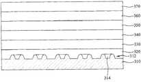
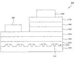
图3A例示了根据本发明的第一实施方式的半导体发光设备的结构。如图3A所示,根据本发明的第一实施方式的半导体发光设备包括:其上形成有一个或更多个凸部的基板310,缓冲层320,未掺杂半导体层330,N型氮化物半导体层340,有源层350,P型氮化物半导体层360,透明电极层370,P型电极380和N型电极390。FIG. 3A illustrates the structure of a semiconductor light emitting device according to a first embodiment of the present invention. As shown in FIG. 3A, the semiconductor light emitting device according to the first embodiment of the present invention includes: a
由于在商业上不能获得如下这样的基板,该基板具有与其上生长的氮化物半导体材料的晶体相同的晶体结构同时呈现晶格匹配,因此考虑到晶格匹配,蓝宝石(sapphire)基板主要用作基板310。Since a substrate having the same crystal structure as a crystal of a nitride semiconductor material grown thereon while exhibiting lattice matching cannot be commercially obtained, a sapphire substrate is mainly used as a substrate in consideration of lattice matching 310.
蓝宝石基板是具有Hexa-Rhombo R3c对称的晶体,该晶体具有这样的特性:在c轴方向上晶格常数为13.001

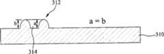
为了提高光出射效率和基板310上生长的氮化物半导体材料的质量,在根据本发明的第一实施方式的半导体发光设备100的基板310上形成一个或更多个凸部312,如图3A所示。在这种情况下,可以通过蚀刻基板310来形成凸部312。In order to improve the light emission efficiency and the quality of the nitride semiconductor material grown on the
根据本发明的一个实施方式,在各凸部312中形成凹部314,使得基板310的表面能够通过凸部312的凹部314而露出。这是为了增大其上生长半导体材料的基板310的表面积。即,该半导体材料能够在凸部312的凹部314中基板310的表面上生长,由此来增加其上能够生长半导体材料的基板310的表面积。According to one embodiment of the present invention, a
如图4A所示,凹部314在凸部312中形成,其中,基板310的通过凹部314露出的表面是平坦的,并且具有c(0001)平面的方向性。即,凹部314的平坦底面使得半导体材料平坦地生长在凸部312中基板310的表面上。结果,可以提供基板310上生长的半导体层的质量,并且还能够降低半导体层的位错密度。As shown in FIG. 4A , a
如图4A所示,凸部312内的凹部314的深度(a)可以与凸部312的高度(b)相同。然而,本发明的改进实施方式公开了凹部314的深度(a)大于凸部312的高度(b),如图4B所示。如果凹部314的深度(a)大于凸部312的高度(b)(即,a>b),则凹部314的底面低于基板310的上表面,由此由于增大使光发生全反射的角度和面积而提高了光出射效率。As shown in FIG. 4A , the depth (a) of the
本发明的另一改进实施方式公开了凹部314的深度(a)小于凸部312的高度(b)(即,a<b),如图4C所示。在这种情况下,凸部312的内底表面会通过凹部314露出。优选地,凸部312的通过凹部314露出的内底表面是平坦的,并且具有c(0001)平面的方向性。Another improved embodiment of the present invention discloses that the depth (a) of the
当形成根据本发明的前述实施方式的凸部312时,凸部312在水平截面图中的面积从其底部316到顶部317逐渐减小,其中,凸部312的底部与基板310接触。同时,以凹部314在水平截面图中的面积从其底部318到顶部317逐渐增大的方式来形成凸部312内的凹部314,其中,凹部314的底部位于基板310的上表面附近。When forming the
例如,可以以凸部312的一个垂直截面为半圆形的方式来形成凸部312,如图5A所示;或者,可以以凸部312的一个垂直截面为诸如三角形的多边形的方式来形成凸部312,如图5B所示。For example, the
图3B示出了位于基板310上的前述凸部312的一个示例。如图3B所示,已知凸部312设置有凹部314,该凹部314使得基板310的表面能够露出。此时,可以在基板310上规则地或者不规则地设置多个凸部312。FIG. 3B shows an example of the
图3B例示了其中具有凹部314的环形凸部312。但是,凸部312的形状并不限于前述环状。例如,可以以诸如三角形环状或矩形环状的多边形环状来形成凸部312。FIG. 3B illustrates an
本发明的前述实施方式公开了蓝宝石基板用作基板310。作为选择,基板310可以由GaN、SiC、ZnO、GaP、GaAs或导电材料形成。The foregoing embodiments of the present invention disclosed a sapphire substrate as the
再次参照图3A,设置缓冲层320以减小基板310和N型氮化物半导体层340之间的晶格常数差。在包括凸部312的基板310上形成缓冲层320。缓冲层320可以选择性地以AlInN结构、InGaN/GaN超晶格结构、InGaN/GaN层叠结构或AlInGaN/InGaN/GaN层叠结构来形成。Referring again to FIG. 3A , the
在缓冲层320上形成未掺杂半导体层330,其中,未掺杂半导体层330可以由基于GaN的材料形成。例如,可以通过在1500℃的温度下提供NH3和三金属镓(tri-metal gallium,TMGa)来在缓冲层320上形成未掺杂半导体层。An
本发明的前述实施方式既包括缓冲层320又包括未掺杂半导体层330。然而,本发明的改进实施方式可以包括缓冲层320和未掺杂半导体层330中的任何一个,或者可以不包括缓冲层320也不包括未掺杂半导体层330。The foregoing embodiments of the present invention include both the
在未掺杂半导体层330上形成N型氮化物半导体层340。通常,N型氮化物半导体层340由GaN、AlGaN、InGaN、AlN或AlInGaN形成。在这种情况下,用于形成N型氮化物半导体层340的掺杂剂可以是Si、Ge、Sn、Se或Te。The N-type
可以通过MOCVD(金属有机化学气相沉积)、MBE(分子束外延)或HVPE(氢化物气相外延)在基板310上生长前述半导体材料来形成N型氮化物半导体层340。The N-type
设置有源层350来进行发光,光是在由InGaN层形成阱而由(Al)GaN层形成势垒层(barrier layer)的条件下通过形成多重量子阱(MQW)而获得的。蓝色发光二极管使用InGaN/GaN的多重量子阱结构,而紫外发光二极管使用GaN/AlGaN、InAlGaN/InAlGaN或InGaN/AlGaN的多重量子阱结构。对于提高有源层350中的效率,可以通过改变In或Al的成分来控制光波长;或者可以通过改变有源层350中阱的深度、有源层350的数量和有源层350的厚度来提高内量子效率。The
可以通过MOCVD(金属有机气相沉积)、MBE(分子束外延)或HVPE(氢化物气相外延)在N型氮化物半导体层340上形成有源层350。The
在有源层350上形成P型氮化物半导体层360,其中,P型氮化物半导体层360可以由诸如GaN、AlGaN、InGaN、AlN或AlInGaN的典型的基于氮化物的半导体材料形成。在这种情况下,用于形成P型半导体层360的掺杂剂可以是Mg、Zn或Be。A P-type
可以通过MOCVD(金属有机气相沉积)、MBE(分子束外延)或HVPE(氢化物气相外延)在有源层350上生长前述基于氮化物的半导体材料,来形成P型氮化物半导体层360。The P-type
在P型氮化物半导体层360上形成透明电极层370。优选地,透明电极层370由能够减小对于具有相对高能量带隙并且具有较好的透光属性的P型氮化物半导体层360的接触电阻的材料形成,以便由此向上透射有源层350中产生的光。A
通常,在Ni/Au的双层结构中形成透明电极层370。优选地,透明电极层370由诸如氧化铟锡(ITO)、氧化镉锡(CTO)或钛钨氮化物(TiWN)的预定材料形成。用于透明电极层370的前述预定材料可以实现良好的透光属性,但其接触电阻相对较高。Generally, the
可以通过诸如MOCVD(金属有机气相沉积)或MBE(分子束外延)的沉积方法来形成透明电极层370;或者可以通过溅射来形成透明电极层370。此时,进行大约400℃到900℃的热处理以改善欧姆接触属性。The
在透明电极层370上形成P型电极380。P型电极380通常可以通过诸如MOCVD(金属有机气相沉积)或MBE(分子束外延)的沉积方法或者通过溅射来由金(Au)或者含金(Au)的合金形成。A P-
在被台面蚀刻的N型氮化物半导体层340上形成N型电极390,其中,可以使用从Ti、Cr、Al、Cu和Au的材料组中选择的材料以单层结构或多层结构形成N型电极390。N型电极390可以通过诸如MOCVD(金属有机化学气相沉积)或MBE(分子束外延)的沉积方法或者通过溅射来在N型氮化物半导体层340上形成。The N-
参照图6,现在来描述根据本发明的第一实施方式的发光设备的制造方法。图6A到6E是例示了根据本发明的第一实施方式的半导体发光设备的制造方法的截面图。Referring to FIG. 6, a method of manufacturing the light emitting device according to the first embodiment of the present invention will now be described. 6A to 6E are cross-sectional views illustrating a method of manufacturing a semiconductor light emitting device according to a first embodiment of the present invention.
参照图6A,在基板310上形成掩模图案610,其中,掩模图案610由光刻胶、聚合物、氧化物层(SiO2)、氮化物层(SiNx)或金属薄膜形成。设置掩模图案610以形成其中具有凹部314的凸部312。Referring to FIG. 6A, a
将简要说明通过使用光刻胶来形成掩模图案610的过程。首先,在用光刻胶对基板310进行涂敷之后,通过使用用于形成图案的掩模对光刻胶进行曝光和显影,由此在基板310上形成期望的掩模图案。A process of forming the
然后,如图6B所示,在对其上形成有掩模图案610的基板310进行蚀刻之后,从基板310移除掩模图案610,由此形成一个或更多个凸部312,其中,各凸部312中设置有凹部314。根据本发明的一个实施方式,可以通过湿蚀刻或等离子体蚀刻来对基板310进行蚀刻。如果应用湿蚀刻,则可以通过使用从包括Cl2、BCl3、HCl和CCl4的组中选择的基于Cl的气体或者通过使用从包括HBr、HF、Hl、H2SO4、NHO3和H3PO4的组中选择的酸来对基板310进行蚀刻。Then, as shown in FIG. 6B, after etching the
根据本发明,其中设置有凹部314的凸部312形成在基板310上,以增加基板310的用于生长半导体层的表面面积。在这种情况下,该半导体材料能够在凸部312内的底表面上生长,由此来增加基板310上生长半导体层的表面面积。According to the present invention, the
当通过蚀刻在基板310上形成凸部312时,如图4A所示,在凸部312中形成凹部314,其中,基板310的通过凹部314露出的表面是平坦的并且具有C平面的方向属性。即,凸部312内的平坦底面使得半导体材料平坦地生长在凸部312中基板310的表面上。结果,可以提高表面310上生长的半导体层的质量。When the
在这种情况下,凸部312内部的凹部314的深度(a)可以与凸部312的高度(b)相同,如图4A所示。如图4B所示,凹部314的深度(a)可以大于凸部312的高度(b)。In this case, the depth (a) of the
如图4C所示,凹部314的深度(a)小于凸部312的高度(b)。在这种情况下,凸部312的内底表面将通过凹部314露出。优选地,凸部312的通过凹部314露出的内底表面是平坦的,并且具有C平面的方向属性。As shown in FIG. 4C , the depth (a) of the
当形成根据本发明的前述实施方式的凸部312时,凸部312在水平截面图中的面积从其底部316到顶部317逐渐减小,其中,凸部312的底部与基板310接触。同时,以凹部314在水平截面图中的面积从其底部318到顶部317逐渐增大的方式来形成凸部312的凹部314,其中,凹部314的底部位于基板310的上表面附近。When forming the
例如,可以以凸部312的一个垂直截面为半圆形的方式形成凸部312,如图5A所示;或者,可以以凸部312的一个垂直截面为诸如三角形的多边形的方式形成凸部312,如图5B所示。For example, the
如图6C所示,在具有凸部312的基板310上顺序形成缓冲层320、未掺杂半导体层330、N型氮化物半导体层340、有源层350、P型氮化物半导体层360和透明电极层370。至少可以形成缓冲层320和未掺杂半导体层330中的任何一个;或者可以既不形成缓冲层320也不形成未掺杂半导体层330。As shown in FIG. 6C, a
如图6D所示,为了形成N型电极390,到N型氮化物半导体层340为止,应用台面蚀刻。As shown in FIG. 6D , in order to form the N-
如图6E所示,在透明电极层370上形成P型电极380,而在N型氮化物半导体层340上形成N型电极390。As shown in FIG. 6E , a P-
为了提高半导体发光设备的可靠性,尽管未示出,但是在半导体发光设备的整个区域上形成使用了诸如SiO2的氧化物的绝缘层;通过研磨和抛光工艺使所形成的绝缘层变薄;然后,通过使用激光或金刚石(diamond)的划线工艺将半导体发光设备分成单个的芯片。In order to improve the reliability of the semiconductor light emitting device, although not shown, an insulating layer using an oxide such as SiO2 is formed on the entire area of the semiconductor light emitting device; the formed insulating layer is thinned through grinding and polishing processes; Then, the semiconductor light emitting devices are divided into individual chips by a scribing process using laser or diamond.
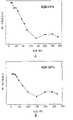
图7是通过将相关技术的半导体发光设备中的内量子效率(IQE)与根据本发明的第一实施方式的半导体发光设备中的IQE进行比较,示出了根据本发明的第一实施方式的半导体发光设备中的IQE的提高的图。FIG. 7 is a graph showing the internal quantum efficiency (IQE) according to the first embodiment of the present invention by comparing the internal quantum efficiency (IQE) in the semiconductor light emitting device of the related art with the IQE in the semiconductor light emitting device according to the first embodiment of the present invention. Graph of improvement of IQE in semiconductor light emitting devices.
没有设置凸部的相关技术的半导体发光设备仅呈现出21%的IQE,如图7A所示。同时,根据本发明的第一实施方式的半导体发光设备在基板310上设置有凸部312,并呈现出32%的IQE,如图7B所示。与相关技术的半导体发光设备相比,根据本发明的第一实施方式的半导体发光设备在IQE上能够提高10%。The semiconductor light emitting device of the related art not provided with convex portions exhibited an IQE of only 21%, as shown in FIG. 7A . Meanwhile, the semiconductor light emitting device according to the first embodiment of the present invention is provided with a
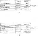
图8是通过将相关技术的半导体发光设备中的光出射效率与根据本发明的第一实施方式的半导体发光设备中的光出射效率进行比较,示出了根据本发明的第一实施方式的半导体发光设备中的光出射效率的提高的表。FIG. 8 is a graph showing the semiconductor light emission efficiency according to the first embodiment of the present invention by comparing the light emission efficiency in the semiconductor light emitting device of the related art with the light emission efficiency in the semiconductor light emitting device according to the first embodiment of the present invention. Table of improvement of light extraction efficiency in a light emitting device.
没有设置凸部的相关技术的半导体发光设备仅呈现出26%的光出射效率,如图8A所示。同时,根据本发明的第一实施方式的半导体发光设备在基板310上设置有凸部312,并呈现出约69%的光出射效率,如图8B所示。与相关技术的半导体发光设备相比,根据本发明的第一实施方式的半导体发光设备在光出射效率上能够提高40%。The semiconductor light emitting device of the related art that is not provided with convex portions exhibits only 26% light extraction efficiency, as shown in FIG. 8A . Meanwhile, the semiconductor light emitting device according to the first embodiment of the present invention is provided with a
第二实施方式second embodiment
根据本发明的第一实施方式的前述半导体发光设备公开了仅在基板上设置有凸部。然而,根据本发明的第二实施方式的半导体发光设备公开了除了在基板上还可以在P型氮化物半导体层上形成凸部,以提高透光效率。以下,参照图9来描述根据本发明的第二实施方式的半导体发光设备。The aforementioned semiconductor light emitting device according to the first embodiment of the present invention discloses that the protrusions are provided only on the substrate. However, the semiconductor light emitting device according to the second embodiment of the present invention discloses that protrusions may be formed on the P-type nitride semiconductor layer in addition to the substrate to improve light transmission efficiency. Hereinafter, a semiconductor light emitting device according to a second embodiment of the present invention is described with reference to FIG. 9 .
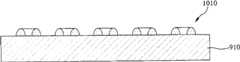
如图9所示,根据本发明的第二实施方式的半导体发光设备包括:其上形成有一个或更多个第一凸部912的基板910,缓冲层920,未掺杂半导体层930,N型氮化物半导体层940,有源层950,其上形成有一个或更多个第二凸部962的P型氮化物半导体层960,透明电极层970,P型电极980和N型电极990。As shown in FIG. 9, the semiconductor light emitting device according to the second embodiment of the present invention includes: a
以与根据本发明的第一实施方式的半导体发光设备相同的方式,根据本发明的第二实施方式的半导体发光设备公开了在具有一个或更多个第一凸部912的基板910上顺序形成缓冲层920、未掺杂半导体层930、N型氮化物半导体层940、以及有源层950,其中,各第一凸部912中设置有凹部914。即,根据本发明的第二实施方式的半导体发光设备中设置的第一凸部912、基板910、缓冲层920、未掺杂半导体层930、N型氮化物半导体层940以及有源层950与根据本发明的第一实施方式的半导体发光设备中的相同,由此将省略对根据本发明的第二实施方式的半导体发光设备中设置的第一凸部912、基板910、缓冲层920、未掺杂半导体层930、N型氮化物半导体层940以及有源层950的详细说明。In the same manner as the semiconductor light emitting device according to the first embodiment of the present invention, the semiconductor light emitting device according to the second embodiment of the present invention discloses sequentially forming on a
如图9所示,为了实现更好的光出射效率,在P型氮化物半导体层960上形成一个或更多个第二凸部962。此时,可以通过蚀刻P型氮化物半导体层960来形成第二凸部962。As shown in FIG. 9 , in order to achieve better light extraction efficiency, one or more
根据本发明的一个实施方式,在P型氮化物半导体层960上形成第二凸部962。以第二凸部962的一个垂直截面为半圆形的方式形成第二凸部962,如图9所示。这种半圆形的第二凸部962能够增加光散射,由此提高光出射效率。According to one embodiment of the present invention, the
根据本发明的另一个实施方式,第二凸部962可以在一个垂直截面的形状上与第一凸部912相同。即,可以在第二凸部962中形成凹部(未示出),使得P型氮化物半导体层960的表面或者第二凸部962的内表面能够通过第二凸部962的凹部露出。According to another embodiment of the present invention, the second
更详细地,第二凸部962内的凹部深度可以等于或大于第二凸部962的高度,由此P型氮化物半导体层960的表面能够通过第二凸部962的凹部露出。另外,第二凸部962内的凹部深度可以小于第二凸部962的高度,由此第二凸部962的内表面能够通过第二凸部962的凹部露出。In more detail, the depth of the recess in the
在这种情况下,优选地,P型氮化物半导体层960的通过凹部露出的表面或者第二凸部的通过凹部露出的内表面是平坦的。In this case, preferably, the surface of the P-type
当形成第二凸部962时,第二凸部962在水平截面图中的面积从其底部到顶部逐渐减小,其中,第二凸部的底部与P型氮化物半导体层960接触。同时,以凹部在水平截面图中的面积从其底部到顶部逐渐增大的方式形成第二凸部962内的凹部,其中,凹部的底部位于P型氮化物半导体层960的上表面附近。When forming the
以与第一凸部912相同的方式,可以以第二凸部962的一个垂直截面为半圆形或诸如三角形的多边形的方式形成第二凸部962。In the same manner as the first
如前述附图中所示,第二凸部962在高度和图案上与第一凸部912相同。然而,本发明的改进实施方式可以公开第二凸部962在高度和图案上与第一凸部912不同。As shown in the preceding figures, the
同时,透明电极层970、P型电极980和N型电极990分别与图3中的透明电极层370、P型电极380和N型电极390相同。因此,将省略对透明电极层970、P型电极980和N型电极990的详细说明。Meanwhile, the
以下,参照图10来描述根据本发明的第二实施方式的半导体发光设备的制造方法。图10A到10G是例示了根据本发明的第二实施方式的半导体发光设备的制造方法的截面图。Hereinafter, a method of manufacturing a semiconductor light emitting device according to a second embodiment of the present invention will be described with reference to FIG. 10 . 10A to 10G are cross-sectional views illustrating a method of manufacturing a semiconductor light emitting device according to a second embodiment of the present invention.
图10A和10B例示了在基板910上形成具有凹部914的一个或更多个凸部912的步骤,其与图6A和6B相同,因此将省略对图10A和10B的详细说明。FIGS. 10A and 10B illustrate steps of forming one or
如图10C所示,在包括第一凸部912的基板910上顺序形成缓冲层920、未掺杂半导体层930、N型氮化物半导体层940、有源层950和P型氮化物半导体层960。至少可以形成缓冲层920和未掺杂半导体层930中的任何一个;或者可以既不形成缓冲层920也不形成未掺杂半导体层930。As shown in FIG. 10C, a
如图10D所示,在P型氮化物半导体层960上形成用于形成第二凸部962的掩模图案1020,其中,掩模图案1020通过使用光刻胶、聚合物、氧化物层(SiO2)、氮化物层(SiNx)或金属薄膜形成。将简要说明通过使用光刻胶形成掩模图案1020的过程。在用光刻胶对P型氮化物半导体层960进行涂敷之后,通过使用用于形成图案的掩模对光刻胶进行曝光和显影,由此在P型氮化物半导体层960上形成期望的掩模图案1020。As shown in FIG. 10D, a
如图10E所示,在对其上形成有掩模图案1020的P型氮化物半导体层960进行蚀刻之后,从P型氮化物半导体层960移除掩模图案1020,由此在P型氮化物半导体层960上形成一个或更多个第二凸部962。在这种情况下,可以以第二凸部962的一个垂直截面为半圆形的方式形成第二凸部962,如图9所示;或者可以以第二凸部962的一个垂直截面与第一凸部912的相同的方式形成第二凸部962。As shown in FIG. 10E , after etching the P-type
根据本发明的一个实施方式,可以通过湿蚀刻或等离子体蚀刻来对P型氮化物半导体层960进行蚀刻。如果应用湿蚀刻,则可以通过使用从包括Cl2、BCl3、HCl和CCl4的组中选择的基于的Cl的气体或者通过使用从包括HBr、HF、Hl、H2SO4、NHO3和H3PO4的组中选择的酸来对P型氮化物半导体层960进行蚀刻。According to one embodiment of the present invention, the P-type
为了实现更好的光出射效率,在P型氮化物半导体层960上形成第二凸部962。In order to achieve better light extraction efficiency, the
如图10F所示,在包括第二凸部962的P型氮化物半导体层上形成透明电极层970,然后,为了形成N型电极990,到N型氮化物半导体层940为止,应用台面蚀刻。As shown in FIG. 10F , a
如图10G所示,在透明电极层970上形成P型电极980,而在N型氮化物半导体层940上形成N型电极990。As shown in FIG. 10G , a P-
尽管未示出,但是为了提高半导体发光设备的可靠性,在半导体发光设备的整个区域上形成使用了诸如SiO2的氧化物的绝缘层;通过研磨和抛光工艺使所形成的绝缘层变薄;然后,通过使用激光或金刚石的划线工艺将半导体发光设备分成单个的芯片。Although not shown, in order to improve the reliability of the semiconductor light emitting device, an insulating layer using an oxide such as SiO2 is formed on the entire area of the semiconductor light emitting device; the formed insulating layer is thinned through grinding and polishing processes; Then, the semiconductor light emitting device is divided into individual chips by a scribing process using laser or diamond.
根据本发明,基板上的一个或更多个凸部使得能够出射一些横向光,由此提高了根据本发明的半导体发光设备中的光出射效率。According to the invention, the one or more protrusions on the substrate enable some lateral light to be emitted, thereby improving the light extraction efficiency in the semiconductor light emitting device according to the invention.
而且,凸部内部形成的凹部使得能够由此平坦地露出基板的表面或凸部的内表面,使得能够提高基板上生长的半导体层的质量,而且降低半导体层的位错密度。Also, the recesses formed inside the protrusions make it possible to thereby flatly expose the surface of the substrate or the inner surface of the protrusions, making it possible to improve the quality of the semiconductor layer grown on the substrate and reduce the dislocation density of the semiconductor layer.
此外,可以通过减小半导体层中的位错密度来提高IQE。In addition, IQE can be improved by reducing the dislocation density in the semiconductor layer.
而且,质量得到提高的半导体发光设备能够减小正向电压并增大电流分散。Also, semiconductor light emitting devices with improved quality can reduce forward voltage and increase current dispersion.
对于本领域技术人员明显的是,可以在不脱离本发明的精神或范围的情况下对本发明做出各种修改和变型。因此,本发明旨在涵盖落入所附权利要求及其等同物的范围内的本发明的修改和变型。It will be apparent to those skilled in the art that various modifications and variations can be made in the present invention without departing from the spirit or scope of the inventions. Thus, it is intended that the present invention covers the modifications and variations of this invention that come within the scope of the appended claims and their equivalents.
Claims (20)
Applications Claiming Priority (2)
| Application Number | Priority Date | Filing Date | Title |
|---|---|---|---|
| KR10-2009-0122914 | 2009-12-11 | ||
| KR1020090122914AKR101277445B1 (en) | 2009-12-11 | 2009-12-11 | Semiconductor Light Emitting Device and Method for Manufacturing Thereof |
Publications (2)
| Publication Number | Publication Date |
|---|---|
| CN102097561Atrue CN102097561A (en) | 2011-06-15 |
| CN102097561B CN102097561B (en) | 2014-09-17 |
Family
ID=44130522
Family Applications (1)
| Application Number | Title | Priority Date | Filing Date |
|---|---|---|---|
| CN201010185123.9AExpired - Fee RelatedCN102097561B (en) | 2009-12-11 | 2010-05-20 | Semi-conductor light emitting device and method for manufacturing thereof |
Country Status (4)
| Country | Link |
|---|---|
| US (1) | US8519412B2 (en) |
| KR (1) | KR101277445B1 (en) |
| CN (1) | CN102097561B (en) |
| TW (1) | TWI532211B (en) |
Cited By (3)
| Publication number | Priority date | Publication date | Assignee | Title |
|---|---|---|---|---|
| CN104134728A (en)* | 2013-05-03 | 2014-11-05 | 上海蓝光科技有限公司 | Manufacturing method of light emitting diode |
| CN105742429A (en)* | 2016-03-01 | 2016-07-06 | 聚灿光电科技股份有限公司 | Ultraviolet GaN-based LED epitaxy structure and manufacturing method thereof |
| US9632630B2 (en) | 2011-11-17 | 2017-04-25 | Tera Xtal Technology Corp. | Touch panel structure |
Families Citing this family (14)
| Publication number | Priority date | Publication date | Assignee | Title |
|---|---|---|---|---|
| TW201214802A (en)* | 2010-09-27 | 2012-04-01 | Nat Univ Chung Hsing | Patterned substrate and LED formed using the same |
| EP2668662B1 (en)* | 2011-01-25 | 2019-07-03 | LG Innotek Co., Ltd. | Semiconductor device and method for growing semiconductor crystal |
| US10522714B2 (en) | 2011-06-15 | 2019-12-31 | Sensor Electronic Technology, Inc. | Device with inverted large scale light extraction structures |
| US10319881B2 (en)* | 2011-06-15 | 2019-06-11 | Sensor Electronic Technology, Inc. | Device including transparent layer with profiled surface for improved extraction |
| KR101987056B1 (en)* | 2012-11-07 | 2019-06-10 | 엘지이노텍 주식회사 | Light emitting device and light emitting device package |
| KR102008363B1 (en)* | 2013-07-09 | 2019-08-07 | 엘지이노텍 주식회사 | Light emitting device and lighting system |
| KR102065776B1 (en)* | 2013-07-12 | 2020-01-13 | 엘지이노텍 주식회사 | Light emitting device |
| KR102232756B1 (en) | 2014-05-19 | 2021-03-26 | 삼성전자주식회사 | Electronic device having graphene-semiconductor multi junction and method of manufacturing the same |
| JP6375890B2 (en) | 2014-11-18 | 2018-08-22 | 日亜化学工業株式会社 | Nitride semiconductor device and manufacturing method thereof |
| CN104967430B (en)* | 2015-07-01 | 2017-06-09 | 东南大学 | Gallium nitride base low-leakage current clamped beam switchs the rest-set flip-flop of nor gate |
| CN105141288B (en)* | 2015-07-01 | 2018-02-13 | 东南大学 | Rest-set flip-flop based on GaAs base low-leakage current double cantilever beam switch nor gate |
| CN105049001B (en)* | 2015-07-01 | 2017-07-28 | 东南大学 | Rest-set flip-flop based on the cantilever switch of GaAs base low-leakage current four |
| CN104935290B (en)* | 2015-07-01 | 2017-07-28 | 东南大学 | The SCF and preparation method of silicon substrate low-leakage current clamped beam grid |
| KR102542229B1 (en)* | 2015-10-15 | 2023-06-12 | 쑤저우 레킨 세미컨덕터 컴퍼니 리미티드 | Light emitting device and light emitting device including the same |
Citations (2)
| Publication number | Priority date | Publication date | Assignee | Title |
|---|---|---|---|---|
| US20050179130A1 (en)* | 2003-08-19 | 2005-08-18 | Hisanori Tanaka | Semiconductor device |
| US20080286893A1 (en)* | 2005-06-16 | 2008-11-20 | Samsung Electro-Mechanics Co., Ltd. | Light emitting device having protrusion and recess structure and method of manufacturing the same |
Family Cites Families (5)
| Publication number | Priority date | Publication date | Assignee | Title |
|---|---|---|---|---|
| JP4356723B2 (en)* | 2001-07-24 | 2009-11-04 | 日亜化学工業株式会社 | Manufacturing method of nitride semiconductor light emitting device |
| KR20060065869A (en)* | 2004-12-10 | 2006-06-14 | 엘지전자 주식회사 | High light extraction efficiency light emitting diode |
| KR101338698B1 (en)* | 2007-04-16 | 2013-12-06 | 엘지이노텍 주식회사 | Nitride semiconductor light emitting device |
| TWI357886B (en) | 2007-08-13 | 2012-02-11 | Epistar Corp | Stamp having nanometer scale structure and applica |
| KR100882240B1 (en)* | 2008-09-11 | 2009-02-25 | (주)플러스텍 | Nitride semiconductor light emitting device and manufacturing method |
- 2009
- 2009-12-11KRKR1020090122914Apatent/KR101277445B1/ennot_activeExpired - Fee Related
- 2010
- 2010-04-30TWTW099113954Apatent/TWI532211B/ennot_activeIP Right Cessation
- 2010-05-20CNCN201010185123.9Apatent/CN102097561B/ennot_activeExpired - Fee Related
- 2010-07-15USUS12/837,274patent/US8519412B2/enactiveActive
Patent Citations (2)
| Publication number | Priority date | Publication date | Assignee | Title |
|---|---|---|---|---|
| US20050179130A1 (en)* | 2003-08-19 | 2005-08-18 | Hisanori Tanaka | Semiconductor device |
| US20080286893A1 (en)* | 2005-06-16 | 2008-11-20 | Samsung Electro-Mechanics Co., Ltd. | Light emitting device having protrusion and recess structure and method of manufacturing the same |
Cited By (4)
| Publication number | Priority date | Publication date | Assignee | Title |
|---|---|---|---|---|
| US9632630B2 (en) | 2011-11-17 | 2017-04-25 | Tera Xtal Technology Corp. | Touch panel structure |
| CN104134728A (en)* | 2013-05-03 | 2014-11-05 | 上海蓝光科技有限公司 | Manufacturing method of light emitting diode |
| CN104134728B (en)* | 2013-05-03 | 2018-10-09 | 上海蓝光科技有限公司 | A kind of manufacturing method of light emitting diode |
| CN105742429A (en)* | 2016-03-01 | 2016-07-06 | 聚灿光电科技股份有限公司 | Ultraviolet GaN-based LED epitaxy structure and manufacturing method thereof |
Also Published As
| Publication number | Publication date |
|---|---|
| KR20110066311A (en) | 2011-06-17 |
| US20110140127A1 (en) | 2011-06-16 |
| US8519412B2 (en) | 2013-08-27 |
| KR101277445B1 (en) | 2013-06-27 |
| CN102097561B (en) | 2014-09-17 |
| TW201121099A (en) | 2011-06-16 |
| TWI532211B (en) | 2016-05-01 |
Similar Documents
| Publication | Publication Date | Title |
|---|---|---|
| CN102097561B (en) | Semi-conductor light emitting device and method for manufacturing thereof | |
| KR101125395B1 (en) | Light emitting device and fabrication method thereof | |
| KR100661614B1 (en) | Nitride-based semiconductor light emitting device and its manufacturing method | |
| JP6934812B2 (en) | Light emitting element and light emitting element array including it | |
| EP2156478B1 (en) | Semiconductor light emitting device and method of manufacturing the same | |
| US8987768B2 (en) | Semiconductor light emitting device having roughness layer | |
| US8410506B2 (en) | High efficiency light emitting diode | |
| EP2232594B1 (en) | Semiconductor light emitting device and method of fabricating the same | |
| US11810943B2 (en) | Light-emitting device and manufacturing method thereof | |
| US20080044937A1 (en) | Method of forming surface irregularities and method of manufacturing gallium nitride-based light emitting diode | |
| US20110114980A1 (en) | Semiconductor light-emitting device and method for manufacturing the same | |
| KR20110052131A (en) | Light emitting device and manufacturing method | |
| KR101081129B1 (en) | Light emitting device and fabrication method thereof | |
| US20140206120A1 (en) | Light emitting diode and method for fabricating the same | |
| KR20090076163A (en) | Nitride semiconductor light emitting device manufacturing method and nitride semiconductor light emitting device manufactured thereby | |
| US20130087763A1 (en) | Light emitting diode and method of manufacturing the same | |
| TWI437731B (en) | Semiconductor optoelectronic component with improved light extraction rate and method of manufacturing same | |
| US9306120B2 (en) | High efficiency light emitting diode | |
| KR20120128961A (en) | Semiconductor Light Emitting Device and Manufacturing Method of The Same | |
| KR100999695B1 (en) | Semiconductor light emitting device and manufacturing method thereof | |
| TWI845841B (en) | Light-emitting device | |
| TWI786276B (en) | Manufacturing method of light-emitting device | |
| JP2006295057A (en) | Semiconductor light emitting element and its manufacturing method | |
| CN118173683A (en) | Light emitting diode and light emitting device | |
| KR20120010351A (en) | Manufacturing method of semiconductor light emitting device |
Legal Events
| Date | Code | Title | Description |
|---|---|---|---|
| C06 | Publication | ||
| PB01 | Publication | ||
| C10 | Entry into substantive examination | ||
| SE01 | Entry into force of request for substantive examination | ||
| C14 | Grant of patent or utility model | ||
| GR01 | Patent grant | ||
| CF01 | Termination of patent right due to non-payment of annual fee | Granted publication date:20140917 | |
| CF01 | Termination of patent right due to non-payment of annual fee |