CN102097428A - Integrated circuit wafer and integrated circuit wafer cutting method - Google Patents
Integrated circuit wafer and integrated circuit wafer cutting methodDownload PDFInfo
- Publication number
- CN102097428A CN102097428ACN2009102540484ACN200910254048ACN102097428ACN 102097428 ACN102097428 ACN 102097428ACN 2009102540484 ACN2009102540484 ACN 2009102540484ACN 200910254048 ACN200910254048 ACN 200910254048ACN 102097428 ACN102097428 ACN 102097428A
- Authority
- CN
- China
- Prior art keywords
- wafer substrate
- integrated circuit
- wafer
- protective layer
- integrated circuits
- Prior art date
- Legal status (The legal status is an assumption and is not a legal conclusion. Google has not performed a legal analysis and makes no representation as to the accuracy of the status listed.)
- Pending
Links
- 238000000034methodMethods0.000titleclaimsabstractdescription31
- 238000005520cutting processMethods0.000titleclaimsabstractdescription20
- 239000000758substrateSubstances0.000claimsabstractdescription107
- 238000012360testing methodMethods0.000claimsabstractdescription44
- 239000011241protective layerSubstances0.000claimsabstractdescription40
- 239000013078crystalSubstances0.000claimsabstractdescription15
- 239000011159matrix materialSubstances0.000claimsabstractdescription8
- 238000009826distributionMethods0.000claimsabstractdescription6
- 239000010410layerSubstances0.000claimsdescription24
- 230000008569processEffects0.000claimsdescription15
- 238000005530etchingMethods0.000claimsdescription8
- 235000012431wafersNutrition0.000description109
- VYPSYNLAJGMNEJ-UHFFFAOYSA-NSilicium dioxideChemical compoundO=[Si]=OVYPSYNLAJGMNEJ-UHFFFAOYSA-N0.000description8
- 238000002161passivationMethods0.000description8
- 238000005516engineering processMethods0.000description6
- 239000004065semiconductorSubstances0.000description6
- 229910052581Si3N4Inorganic materials0.000description4
- 238000010586diagramMethods0.000description4
- 239000002184metalSubstances0.000description4
- 235000012239silicon dioxideNutrition0.000description4
- 239000000377silicon dioxideSubstances0.000description4
- HQVNEWCFYHHQES-UHFFFAOYSA-Nsilicon nitrideChemical compoundN12[Si]34N5[Si]62N3[Si]51N64HQVNEWCFYHHQES-UHFFFAOYSA-N0.000description4
- 238000005229chemical vapour depositionMethods0.000description3
- 238000005240physical vapour depositionMethods0.000description3
- 239000003990capacitorSubstances0.000description2
- 238000004519manufacturing processMethods0.000description2
- 239000000463materialSubstances0.000description2
- 238000012986modificationMethods0.000description2
- 230000004048modificationEffects0.000description2
- 238000001020plasma etchingMethods0.000description2
- 238000003631wet chemical etchingMethods0.000description2
- XUIMIQQOPSSXEZ-UHFFFAOYSA-NSiliconChemical compound[Si]XUIMIQQOPSSXEZ-UHFFFAOYSA-N0.000description1
- 238000007792additionMethods0.000description1
- 230000008901benefitEffects0.000description1
- 230000015572biosynthetic processEffects0.000description1
- 239000003795chemical substances by applicationSubstances0.000description1
- 239000011248coating agentSubstances0.000description1
- 238000000576coating methodMethods0.000description1
- 230000006872improvementEffects0.000description1
- 239000012535impuritySubstances0.000description1
- 230000003287optical effectEffects0.000description1
- 238000004806packaging method and processMethods0.000description1
- 229920002120photoresistant polymerPolymers0.000description1
- 229910052710siliconInorganic materials0.000description1
- 239000010703siliconSubstances0.000description1
- 239000000126substanceSubstances0.000description1
- 238000006467substitution reactionMethods0.000description1
Images


Landscapes
- Dicing (AREA)
Abstract
Description
Translated fromChinese技术领域technical field
本发明是关于一种集成电路晶圆以及一种集成电路晶圆切割方法。其中,可藉由集成电路晶圆切割方法形成集成电路晶粒。The invention relates to an integrated circuit wafer and an integrated circuit wafer cutting method. Wherein, the integrated circuit die can be formed by cutting the integrated circuit wafer.
背景技术Background technique
硅晶圆是目前制作集成电路的基底材料(Substrate),透过集成电路制造技术,经过一系列繁复的化学、物理和光学程序,完成的集成电路晶圆上可产生出数以千、百计的晶粒(die)。这些晶粒经由测试、切割、封装等过程,可进一步成为一颗颗具有各种功能的集成电路产品。Silicon wafers are currently the substrate material (Substrate) for making integrated circuits. Through integrated circuit manufacturing technology, after a series of complicated chemical, physical and optical procedures, thousands or hundreds of chips can be produced on the completed integrated circuit wafer. The grain (die). After testing, dicing, packaging and other processes, these dies can further become individual integrated circuit products with various functions.
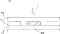
如图1A及图1A中区域80的PP纵切面放大的图1B所示的习知技术,习知集成电路晶圆90包含晶圆基板100、复数个集成电路300、复数个测试键400及保护层500。习知技术进行晶圆切割时通常是以切割刀沿相邻的集成电路300间的路径对集成电路晶圆90施外力K。由于切割时仅以切割刀直接对集成电路晶圆90进行切割,因此,集成电路晶圆90会受切割应力破坏而产生有裂痕及损坏的情形。另一方面,测试键400分布在集成电路300间,亦即在切割路径上,故习知技术在切割时也容易因破坏测试键产生的金属碎屑飞溅至集成电路而导致良率下降。以上集成电路晶圆以及集成电路晶圆切割方法有改善的空间。As shown in Fig. 1A and the prior art shown in Fig. 1B of the enlarged PP longitudinal section of
发明内容Contents of the invention
本发明的主要目的为提供一种集成电路晶圆,分离成集成电路晶粒的良率较高。The main purpose of the present invention is to provide an integrated circuit wafer, which can be separated into integrated circuit crystal grains with a high yield rate.
本发明的另一目的为提供一种集成电路晶圆切割方法,具有较佳的集成电路晶圆切割良率。Another object of the present invention is to provide a method for dicing integrated circuit wafers, which has better dicing yield of integrated circuit wafers.
本发明的集成电路晶圆包含晶圆基板、多个集成电路、多个测试键、保护层以及多条沟槽。集成电路以矩阵分布方式形成于晶圆基板上。测试键分别形成于集成电路之间。一保护层覆盖晶圆基板的集成电路的一侧。沟槽以自保护层表面向下延伸的方式形成于集成电路及测试键之间。The integrated circuit wafer of the present invention includes a wafer substrate, a plurality of integrated circuits, a plurality of test keys, a protection layer and a plurality of grooves. The integrated circuits are formed on the wafer substrate in a matrix distribution manner. Test keys are respectively formed between the integrated circuits. A protective layer covers the integrated circuit side of the wafer substrate. The groove is formed between the integrated circuit and the test key in a manner extending downward from the surface of the protection layer.
测试键是供晶圆基板接受度测试使用。测试键包含晶体管、电容、电阻、N型半导体、P型半导体、复型半导体或金属线元件。保护层包含二氧化硅或氮化硅。沟槽延伸至晶圆基板表面,晶圆基板表面构成沟槽的槽底。沟槽延伸也可进入晶圆基板。沟槽的侧壁为蚀刻表面。沟槽的侧壁为平滑表面。沟槽的侧壁近似垂直。沟槽的侧壁与晶圆基板表面的夹角介于88°至90°。沟槽的宽度小于5μm。The test key is for wafer substrate acceptance testing. The test key includes transistors, capacitors, resistors, N-type semiconductors, P-type semiconductors, complex semiconductors or metal wire components. The protective layer contains silicon dioxide or silicon nitride. The groove extends to the surface of the wafer substrate, and the surface of the wafer substrate forms the groove bottom of the groove. Trench extensions can also be made into the wafer substrate. The sidewalls of the trenches are etched surfaces. The sidewall of the groove is a smooth surface. The sidewalls of the trench are approximately vertical. The included angle between the side wall of the trench and the surface of the wafer substrate is between 88° and 90°. The width of the trench is less than 5 μm.
本发明的集成电路晶圆切割方法,包含以下步骤:于晶圆基板上形成多个集成电路以及多个测试键,其中集成电路是以矩阵分布,测试键分别形成于集成电路之间;形成保护层以覆盖晶圆基板的集成电路的一侧;形成多条沟槽,沟槽以自保护层表面向下延伸的方式形成于集成电路及测试键之间;以及施外力于保护层在两并排相邻的沟槽所夹的区域,使晶圆基板沿两并排相邻沟槽至少其中之一的底部向下沿晶圆基板的晶格分离。The integrated circuit wafer cutting method of the present invention includes the following steps: forming a plurality of integrated circuits and a plurality of test keys on the wafer substrate, wherein the integrated circuits are distributed in a matrix, and the test keys are respectively formed between the integrated circuits; forming protection Layer to cover one side of the integrated circuit of the wafer substrate; form a plurality of grooves, and the grooves are formed between the integrated circuit and the test key in a manner extending downward from the surface of the protective layer; and apply external force to the protective layer on both sides The area between the adjacent trenches enables the wafer substrate to be separated downward along the crystal lattice of the wafer substrate along the bottom of at least one of the two adjacent trenches.
保护层形成步骤包含使用化学气相沉积或物理气相沉积制程形成保护层。沟槽形成步骤包含使用蚀刻制程形成沟槽。沟槽形成步骤包含使沟槽延伸至晶圆基板表面。沟槽形成步骤包含使沟槽延伸进入晶圆基板。形成的沟槽的侧壁近似垂直。沟槽的侧壁与晶圆基板表面的夹角介于88°至90°。沟槽的宽度小于5μm。外力包含以切割刀具沿保护层于两并排相邻的沟槽所夹的区域划压。The protective layer forming step includes forming the protective layer using chemical vapor deposition or physical vapor deposition process. The trench forming step includes forming the trenches using an etching process. The trench forming step includes extending the trench to the surface of the wafer substrate. The trench forming step includes extending the trench into the wafer substrate. The sidewalls of the formed trenches are approximately vertical. The included angle between the side wall of the trench and the surface of the wafer substrate is between 88° and 90°. The width of the trench is less than 5 μm. The external force includes using a cutting tool to draw pressure along the protective layer on the area clamped by two adjacent grooves.
集成电路晶粒包含晶圆基板、集成电路以及保护层。集成电路形成于晶圆基板上。保护层覆盖晶圆基板的集成电路的一侧。其中,晶圆基板及保护层的侧壁分别为平滑表面。晶圆基板的侧壁近似垂直。晶圆基板的侧壁与晶圆基板表面的夹角介于88°至90°。保护层的侧壁近似垂直。保护层的侧壁与晶圆基板表面的夹角介于88°至90°。保护层包含二氧化硅或氮化硅。保护层的侧壁为蚀刻表面。晶圆基板及保护层的侧壁是共平面。晶圆基板的侧壁凸出于保护层的侧壁。晶圆基板的侧壁的上缘与保护层的侧壁是共平面,晶圆基板的侧壁的下部凸出于保护层的侧壁。An integrated circuit die includes a wafer substrate, an integrated circuit, and a protective layer. Integrated circuits are formed on wafer substrates. A protective layer covers the integrated circuit side of the wafer substrate. Wherein, the sidewalls of the wafer substrate and the protection layer are smooth surfaces respectively. The sidewalls of the wafer substrate are approximately vertical. The angle between the sidewall of the wafer substrate and the surface of the wafer substrate is between 88° and 90°. The sidewalls of the protective layer are approximately vertical. The included angle between the sidewall of the protective layer and the surface of the wafer substrate is between 88° and 90°. The protective layer contains silicon dioxide or silicon nitride. The sidewall of the protective layer is an etched surface. The sidewalls of the wafer substrate and the protection layer are coplanar. The sidewall of the wafer substrate protrudes from the sidewall of the protective layer. The upper edge of the side wall of the wafer substrate is coplanar with the side wall of the protective layer, and the lower part of the side wall of the wafer substrate protrudes from the side wall of the protective layer.
本发明的优点是集成电路晶圆的分离成集成电路晶粒的良率高,用本发明的集成电路晶圆切割方法时,具有较佳的集成电路晶圆切割良率。The advantage of the present invention is that the yield rate of separating the integrated circuit wafer into integrated circuit crystal grains is high, and when the integrated circuit wafer cutting method of the present invention is used, it has a better cutting yield rate of the integrated circuit wafer.
附图说明Description of drawings
图1A及图1B为习知技术示意图;1A and 1B are schematic diagrams of conventional technologies;
图2A为本发明实施例上视示意图;Figure 2A is a schematic diagram of an upper view of an embodiment of the present invention;
图2B至图3B为本发明不同实施例示意图;2B to 3B are schematic diagrams of different embodiments of the present invention;
图4A及图4B为本发明较佳实施例示意图;4A and 4B are schematic diagrams of a preferred embodiment of the present invention;
图5为本发明集成电路晶圆切割方法的实施例流程图。FIG. 5 is a flowchart of an embodiment of the method for cutting an integrated circuit wafer according to the present invention.
符号说明Symbol Description
100晶圆基板100 Wafer Substrate
101侧壁101 side wall
110晶圆基板表面110 wafer substrate surface
300集成电路300 integrated circuits
400测试键400 test keys
500保护层500 layers of protection
601路径601 path
602路径602 path
700沟槽700 groove
700’沟槽700' Trench
701侧壁701 side wall
740区域740 area
80区域80 area
800区域800 area
90集成电路晶圆90 integrated circuit wafer
900集成电路晶圆900 integrated circuit wafer
910集成电路晶粒910 integrated circuit die
1011上缘1011 upper edge
1012下部1012 lower part
F外力F external force
K外力K external force
具体实施方式Detailed ways
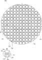
如图2A及图2A中区域800的PP纵切面放大的图2B所示的实施例,本发明的集成电路晶圆900包含晶圆基板100、多个集成电路300、多个测试键400、保护层500以及多条沟槽700。其中,集成电路300是以矩阵分布方式形成于晶圆基板100上。具体而言,在如图2A所示的实施例中,集成电路300以方型为单位,呈矩阵分布方式形成于晶圆基板100上,以便对准进行制造及切割,但不以实施例所示为限。2A and the embodiment shown in FIG. 2B in which the PP longitudinal section of
测试键400分别形成于集成电路300之间。举例而言,测试键400形成于后续用于分割晶圆基板100,而形成含有集成电路300的多个晶粒的切割道上。其中,测试键400供晶圆基板接受度测试(Wafer Acceptance Test)使用。具体而言,可藉由对分布在晶圆基板100上的测试键400进行电性测试获知晶圆基板100的接受度(亦即品质是否良好)。测试键400包含晶体管、电容、电阻、N型半导体、P型半导体、复型半导体或金属线元件等。The
保护层500覆盖晶圆基板100的集成电路300的一侧。具体而言,如图2B所示的实施例,集成电路300及测试键400设置于晶圆基板100上,保护层500同时覆盖集成电路300、测试键400及曝露于集成电路300及测试键400外的晶圆基板100。保护层300较佳包含二氧化硅或氮化硅。其中,保护层300的形成可使用化学气相沉积或物理气相沉积制程。The
如图2A及图2B所示的实施例,沟槽700以自保护层500表面向下延伸的方式形成于集成电路300及测试键400之间。换言之,每一测试键400均以沟槽700与相邻的集成电路300相隔。如图2B所示的实施例,沟槽700延伸至晶圆基板100的表面110,晶圆基板100的表面110构成沟槽700的槽底。在较佳实施例中,沟槽700使用蚀刻制程形成,且较佳使用干式电浆蚀刻制程。然而在不同实施例中,沟槽700也可使用湿式化学蚀刻制程形成。由于沟槽700使用蚀刻制程形成,故沟槽700的侧壁701形成蚀刻表面。如图2B所示,侧壁701的蚀刻表面属于平滑表面,且近似垂直,亦即沟槽700的侧壁701与晶圆基板100的表面110的夹角较佳介于88°至90°。其中,沟槽700的宽度较佳是小于5μm,但不以实施例所示为限。In the embodiment shown in FIG. 2A and FIG. 2B , the
其中,由于晶圆基板100是经由磊晶制程所制成具有整齐晶格的结晶物,故当一外力F施于保护层500在两并排相邻的沟槽700所夹的区域740(例如测试键400所在的区域),晶圆基板100会沿两并排相邻沟槽700至少其中之一的底部向下沿晶圆基板100的晶格分离。例如在图2B所示的实施例中,晶圆基板100沿沟槽700’的底部向下沿晶圆基板100的晶格分离。另一方面,由于晶圆基板100沿晶格分离,晶圆基板100分离后形成的侧壁101会如图3所示为平滑表面。换言之,本发明的集成电路晶圆900无需如习知技术以切割工具强行于集成电路300间进行切割,即可将集成电路晶圆900分离成如图2C所示的集成电路晶粒910。因此,应用本发明技术不仅方便,也不会有习知技术因切割时测试键遭到破坏所产生金属碎屑飞溅至集成电路而导致良率下降的问题。Wherein, since the
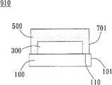
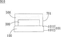
进一步而言,如图2C所示的实施例,本发明的集成电路晶圆900所分离成的集成电路晶粒910包含晶圆基板100、集成电路300以及保护层500。其中,集成电路300形成于晶圆基板100上。保护层500覆盖晶圆基板100的集成电路300的一侧。具体而言,集成电路300设置于晶圆基板100上,保护层500同时覆盖集成电路300及曝露于集成电路300外的晶圆基板100。其中,晶圆基板100的侧壁101及保护层500的侧壁701分别为平滑表面。进一步而言,保护层500的侧壁701即前述图2B的实施例中使用蚀刻制程形成的侧壁701,是蚀刻表面,且近似垂直,亦即侧壁701与晶圆基板100的表面110的夹角介于88°至90°。Further, in the embodiment shown in FIG. 2C , the integrated circuit die 910 separated from the
如图2C所示的实施例,本发明的集成电路晶粒910的晶圆基板100的侧壁101及保护层500的侧壁701是共平面。换言之,如图2B所示,当一外力F施于保护层500在两并排相邻的沟槽700所夹的区域740,晶圆基板100沿路径601向下沿晶圆基板100的晶格分离。分离形成的集成电路晶粒910的保护层500的侧壁701,即如图2C所示延伸与晶圆基板100的侧壁101衔接。其中,侧壁101由晶圆基板100沿晶格分离而形成,其表面性质与平滑的晶圆表面相同。侧壁701由保护层500经蚀刻形成,其表面性质与平滑的保护层表面相同。In the embodiment shown in FIG. 2C , the
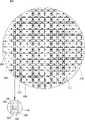
沟槽700的分布方式可视需求而不同,在图2A所示的实施例中,沟槽700为连通晶圆基板100圆周上两点的直线,亦即沟槽700可视为晶圆基板100的弦线。然而在如图2D所示的不同实施例中,沟槽700包围集成电路300的方形线,且相邻的沟槽700方形线彼此不连通。The distribution of
在不同实施例中,由于沟槽700槽底具有一定宽度,晶圆基板100可能自沟槽700槽底的不同位置沿不同路径向下沿晶圆基板100的晶格分离,这是自然发生的现象。如图3A所示,当一外力F施于保护层500在两并排相邻的沟槽700所夹的区域740,晶圆基板100沿路径602向下沿晶圆基板100的晶格分离。分离形成的集成电路晶粒910的晶圆基板100的侧壁101即如图3B所示凸出于保护层500的侧壁701。In different embodiments, since the groove bottom of the
另一方面,如图4A所示的较佳实施例,沟槽700可进一步延伸进入晶圆基板100。当一外力F施于保护层500在两并排相邻的沟槽700所夹的区域740,晶圆基板100沿路径602向下沿晶圆基板100的晶格分离。分离形成的集成电路晶粒910即如图4B所示,晶圆基板100的侧壁101的上缘1011与保护层500的侧壁701是共平面,晶圆基板100的侧壁101的下部1012、凸出于保护层500的侧壁701。On the other hand, the
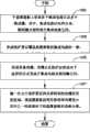
如图5所示,本发明的集成电路晶圆切割方法,包含:As shown in Figure 5, the integrated circuit wafer cutting method of the present invention includes:
步骤1001,于晶圆基板上形成多个集成电路以及多个测试键,其中,集成电路以矩阵分布,测试键分别形成于集成电路之间。具体而言,是以形成氧化膜、涂布感光剂、结合光罩进行曝光、显影、蚀刻、去光阻、以及添加不纯物等步骤,于晶圆基板上形成集成电路以及测试键。其中,可藉由光罩图案控制集成电路以及测试键的形成位置。
步骤1003,形成保护层以覆盖晶圆基板的集成电路的一侧。其中,保护层的形成可使用化学气相沉积或物理气相沉积制程。保护层包含二氧化硅或氮化硅。
步骤1005,形成多条沟槽,沟槽以自保护层表面向下延伸的方式形成于集成电路及测试键之间。沟槽的形成包含使用蚀刻制程,且较佳是使用干式电浆蚀刻制程。然而在不同实施例中,沟槽的形成也可使用湿式化学蚀刻制程或雷射切割。其中,沟槽可如图2B所示延伸至晶圆基板表面110或如图4A所示延伸进入晶圆基板100。
步骤1007,施一外力于保护层在两并排相邻的沟槽所夹的区域,使晶圆基板沿两并排相邻沟槽至少其中之一的底部向下沿晶圆基板的晶格分离。外力包含以切割刀具沿保护层于两并排相邻的沟槽所夹的区域划压。其中,切割刀具在此步骤中做为施力的工具,非强行对晶圆基板进行切割。在不同实施例中,也可以一片状物直接按压保护层于两并排相邻的沟槽所夹的区域,使晶圆基板分离。
虽然前述的描述及图式已揭示本发明的较佳实施例,必须了解到各种增添、许多修改和取代可能使用于本发明较佳实施例,而不会脱离如所附申请专利范围所界定的本发明原理的精神及范围。熟悉本发明所属技术领域的一般技艺者将可体会,本发明可使用于许多形式、结构、布置、比例、材料、元件和元件的修改。因此,本文在此所揭示的实施例应被视为用以说明本发明,而非用以限制本发明。本发明的范围应由后附申请专利范围所界定,并涵盖其合法均等物,并不限于先前的描述。Although the foregoing description and drawings have disclosed preferred embodiments of the present invention, it must be understood that various additions, modifications and substitutions may be applied to the preferred embodiments of the present invention without departing from the scope of the appended patent application spirit and scope of the principles of the invention. Those of ordinary skill in the art to which the invention pertains will appreciate that the invention is applicable to many forms, structures, arrangements, proportions, materials, elements and modifications of elements. Therefore, the embodiments disclosed herein should be regarded as illustrating the present invention rather than limiting the present invention. The scope of the present invention should be defined by the claims of the appended claims and cover their legal equivalents, not limited by the foregoing description.
Claims (10)
Translated fromChinesePriority Applications (1)
| Application Number | Priority Date | Filing Date | Title |
|---|---|---|---|
| CN2009102540484ACN102097428A (en) | 2009-12-15 | 2009-12-15 | Integrated circuit wafer and integrated circuit wafer cutting method |
Applications Claiming Priority (1)
| Application Number | Priority Date | Filing Date | Title |
|---|---|---|---|
| CN2009102540484ACN102097428A (en) | 2009-12-15 | 2009-12-15 | Integrated circuit wafer and integrated circuit wafer cutting method |
Publications (1)
| Publication Number | Publication Date |
|---|---|
| CN102097428Atrue CN102097428A (en) | 2011-06-15 |
Family
ID=44130421
Family Applications (1)
| Application Number | Title | Priority Date | Filing Date |
|---|---|---|---|
| CN2009102540484APendingCN102097428A (en) | 2009-12-15 | 2009-12-15 | Integrated circuit wafer and integrated circuit wafer cutting method |
Country Status (1)
| Country | Link |
|---|---|
| CN (1) | CN102097428A (en) |
Cited By (3)
| Publication number | Priority date | Publication date | Assignee | Title |
|---|---|---|---|---|
| CN103117232A (en)* | 2011-11-16 | 2013-05-22 | 美新半导体(无锡)有限公司 | Wafer-level packaging method and packaging structure thereof |
| CN112687675A (en)* | 2021-03-16 | 2021-04-20 | 荣耀终端有限公司 | Die, module, wafer and manufacturing method of die |
| CN114770781A (en)* | 2022-06-22 | 2022-07-22 | 成都泰美克晶体技术有限公司 | SC wafer chord-changing positioning device and using method thereof |
- 2009
- 2009-12-15CNCN2009102540484Apatent/CN102097428A/enactivePending
Cited By (6)
| Publication number | Priority date | Publication date | Assignee | Title |
|---|---|---|---|---|
| CN103117232A (en)* | 2011-11-16 | 2013-05-22 | 美新半导体(无锡)有限公司 | Wafer-level packaging method and packaging structure thereof |
| CN103117232B (en)* | 2011-11-16 | 2015-07-01 | 美新半导体(无锡)有限公司 | Wafer-level packaging method and packaging structure thereof |
| CN112687675A (en)* | 2021-03-16 | 2021-04-20 | 荣耀终端有限公司 | Die, module, wafer and manufacturing method of die |
| CN112687675B (en)* | 2021-03-16 | 2021-06-29 | 荣耀终端有限公司 | Die, module, wafer and manufacturing method of die |
| CN114770781A (en)* | 2022-06-22 | 2022-07-22 | 成都泰美克晶体技术有限公司 | SC wafer chord-changing positioning device and using method thereof |
| CN114770781B (en)* | 2022-06-22 | 2022-10-14 | 成都泰美克晶体技术有限公司 | SC wafer chord-changing positioning device and using method thereof |
Similar Documents
| Publication | Publication Date | Title |
|---|---|---|
| CN103681661B (en) | Line in wafer | |
| US7952167B2 (en) | Scribe line layout design | |
| US9099547B2 (en) | Testing process for semiconductor devices | |
| US9401343B2 (en) | Method of processing a semiconductor wafer | |
| US10553489B2 (en) | Partitioned wafer and semiconductor die | |
| US8692357B2 (en) | Semiconductor wafer and processing method therefor | |
| TWI469205B (en) | Integrated circuit wafer and dicing method thereof | |
| WO2023019819A1 (en) | Wafer cutting method | |
| US20110256690A1 (en) | Integrated circuit wafer dicing method | |
| CN116779522A (en) | Methods of fabricating semiconductor structures | |
| CN114823315B (en) | Semiconductor device and method for manufacturing the same | |
| TWI689980B (en) | Method of wafer dicing and die | |
| CN102097428A (en) | Integrated circuit wafer and integrated circuit wafer cutting method | |
| CN115295409A (en) | Wafer scribing method | |
| JP6582616B2 (en) | Manufacturing method of semiconductor chip | |
| KR100957185B1 (en) | Wafer processing method for maintaining the quality of upper layer silicon in 3D integrated circuit integration | |
| JP2009140950A (en) | Manufacturing method of semiconductor device | |
| CN100399538C (en) | Method for Reducing Wafer Damage Caused by Shallow Trench Isolation Chemical Mechanical Polishing Process | |
| CN115602625A (en) | Wafer with test structure and method for dicing wafer | |
| JPH10312980A (en) | Manufacture of semiconductor device | |
| JP2007049066A (en) | Semiconductor wafer, semiconductor chip and manufacturing method thereof | |
| TWI892014B (en) | Semiconductor structure and method for manufacturing the same | |
| CN111785686B (en) | Wafer cutting method and grain | |
| TWI433227B (en) | Integrated circuit wafer dicing method | |
| TW451323B (en) | Processing method of forming trench structure on scribe lane |
Legal Events
| Date | Code | Title | Description |
|---|---|---|---|
| C06 | Publication | ||
| PB01 | Publication | ||
| C10 | Entry into substantive examination | ||
| SE01 | Entry into force of request for substantive examination | ||
| C02 | Deemed withdrawal of patent application after publication (patent law 2001) | ||
| WD01 | Invention patent application deemed withdrawn after publication | Application publication date:20110615 |