CN102087568B - Electrical capacitance input device, display apparatus with input function and electronic apparatus - Google Patents
Electrical capacitance input device, display apparatus with input function and electronic apparatusDownload PDFInfo
- Publication number
- CN102087568B CN102087568BCN2011100691449ACN201110069144ACN102087568BCN 102087568 BCN102087568 BCN 102087568BCN 2011100691449 ACN2011100691449 ACN 2011100691449ACN 201110069144 ACN201110069144 ACN 201110069144ACN 102087568 BCN102087568 BCN 102087568B
- Authority
- CN
- China
- Prior art keywords
- wiring
- wirings
- input
- region
- area
- Prior art date
- Legal status (The legal status is an assumption and is not a legal conclusion. Google has not performed a legal analysis and makes no representation as to the accuracy of the status listed.)
- Expired - Fee Related
Links
Images


Classifications
- G—PHYSICS
- G06—COMPUTING OR CALCULATING; COUNTING
- G06F—ELECTRIC DIGITAL DATA PROCESSING
- G06F3/00—Input arrangements for transferring data to be processed into a form capable of being handled by the computer; Output arrangements for transferring data from processing unit to output unit, e.g. interface arrangements
- G06F3/01—Input arrangements or combined input and output arrangements for interaction between user and computer
- G06F3/03—Arrangements for converting the position or the displacement of a member into a coded form
- G06F3/041—Digitisers, e.g. for touch screens or touch pads, characterised by the transducing means
- G06F3/044—Digitisers, e.g. for touch screens or touch pads, characterised by the transducing means by capacitive means
- G06F3/0446—Digitisers, e.g. for touch screens or touch pads, characterised by the transducing means by capacitive means using a grid-like structure of electrodes in at least two directions, e.g. using row and column electrodes
- G—PHYSICS
- G02—OPTICS
- G02F—OPTICAL DEVICES OR ARRANGEMENTS FOR THE CONTROL OF LIGHT BY MODIFICATION OF THE OPTICAL PROPERTIES OF THE MEDIA OF THE ELEMENTS INVOLVED THEREIN; NON-LINEAR OPTICS; FREQUENCY-CHANGING OF LIGHT; OPTICAL LOGIC ELEMENTS; OPTICAL ANALOGUE/DIGITAL CONVERTERS
- G02F1/00—Devices or arrangements for the control of the intensity, colour, phase, polarisation or direction of light arriving from an independent light source, e.g. switching, gating or modulating; Non-linear optics
- G02F1/01—Devices or arrangements for the control of the intensity, colour, phase, polarisation or direction of light arriving from an independent light source, e.g. switching, gating or modulating; Non-linear optics for the control of the intensity, phase, polarisation or colour
- G02F1/13—Devices or arrangements for the control of the intensity, colour, phase, polarisation or direction of light arriving from an independent light source, e.g. switching, gating or modulating; Non-linear optics for the control of the intensity, phase, polarisation or colour based on liquid crystals, e.g. single liquid crystal display cells
- G02F1/133—Constructional arrangements; Operation of liquid crystal cells; Circuit arrangements
- G02F1/1333—Constructional arrangements; Manufacturing methods
- G02F1/13338—Input devices, e.g. touch panels
- G—PHYSICS
- G06—COMPUTING OR CALCULATING; COUNTING
- G06F—ELECTRIC DIGITAL DATA PROCESSING
- G06F3/00—Input arrangements for transferring data to be processed into a form capable of being handled by the computer; Output arrangements for transferring data from processing unit to output unit, e.g. interface arrangements
- G06F3/01—Input arrangements or combined input and output arrangements for interaction between user and computer
- G06F3/03—Arrangements for converting the position or the displacement of a member into a coded form
- G06F3/041—Digitisers, e.g. for touch screens or touch pads, characterised by the transducing means
- G06F3/0412—Digitisers structurally integrated in a display
- G—PHYSICS
- G06—COMPUTING OR CALCULATING; COUNTING
- G06F—ELECTRIC DIGITAL DATA PROCESSING
- G06F3/00—Input arrangements for transferring data to be processed into a form capable of being handled by the computer; Output arrangements for transferring data from processing unit to output unit, e.g. interface arrangements
- G06F3/01—Input arrangements or combined input and output arrangements for interaction between user and computer
- G06F3/03—Arrangements for converting the position or the displacement of a member into a coded form
- G06F3/041—Digitisers, e.g. for touch screens or touch pads, characterised by the transducing means
- G06F3/044—Digitisers, e.g. for touch screens or touch pads, characterised by the transducing means by capacitive means
- G06F3/0443—Digitisers, e.g. for touch screens or touch pads, characterised by the transducing means by capacitive means using a single layer of sensing electrodes
- G—PHYSICS
- G06—COMPUTING OR CALCULATING; COUNTING
- G06F—ELECTRIC DIGITAL DATA PROCESSING
- G06F2203/00—Indexing scheme relating to G06F3/00 - G06F3/048
- G06F2203/041—Indexing scheme relating to G06F3/041 - G06F3/045
- G06F2203/04103—Manufacturing, i.e. details related to manufacturing processes specially suited for touch sensitive devices
- G—PHYSICS
- G06—COMPUTING OR CALCULATING; COUNTING
- G06F—ELECTRIC DIGITAL DATA PROCESSING
- G06F2203/00—Indexing scheme relating to G06F3/00 - G06F3/048
- G06F2203/041—Indexing scheme relating to G06F3/041 - G06F3/045
- G06F2203/04111—Cross over in capacitive digitiser, i.e. details of structures for connecting electrodes of the sensing pattern where the connections cross each other, e.g. bridge structures comprising an insulating layer, or vias through substrate
Landscapes
- Engineering & Computer Science (AREA)
- General Engineering & Computer Science (AREA)
- Theoretical Computer Science (AREA)
- Physics & Mathematics (AREA)
- General Physics & Mathematics (AREA)
- Human Computer Interaction (AREA)
- Nonlinear Science (AREA)
- Mathematical Physics (AREA)
- Chemical & Material Sciences (AREA)
- Crystallography & Structural Chemistry (AREA)
- Optics & Photonics (AREA)
- Position Input By Displaying (AREA)
Abstract
Translated fromChinese
Description
Translated fromChinese本申请为爱普生映像元器件有限公司于2009年3月26日向中国专利局提交的题为“静电电容式输入装置、带输入功能的显示装置及电子设备”的申请号为200910129761.6的中国专利申请的分案申请。This application is the subject of a Chinese patent application with application number 200910129761.6 filed by Epson Imaging Components Co., Ltd. to the China Patent Office on March 26, 2009, entitled "Electrostatic Capacitive Input Device, Display Device with Input Function, and Electronic Equipment" Divisional application.
技术领域technical field
本发明涉及能够检测手指的接触位置来作为静电电容的变化的静电电容式输入装置、带输入功能的显示装置及电子设备。The present invention relates to an electrostatic capacitive input device, a display device with an input function, and electronic equipment capable of detecting the contact position of a finger as a change in electrostatic capacitance.
背景技术Background technique
就便携电话机、汽车导航系统、个人计算机、售票机及银行的终端等电子设备而言,近年来存在着:在液晶装置等的表面配置平板型的输入装置,能通过一边参照液晶装置的图像显示区域上所显示的指示图像、一边用手指等接触显示出该指示图像的部位,来执行与指示图像对应的信息输入的装置。For electronic equipment such as mobile phones, car navigation systems, personal computers, ticket vending machines, and bank terminals, in recent years there have been: a flat-panel input device is arranged on the surface of a liquid crystal device, etc., and the image of the liquid crystal device can be referred to while A device for inputting information corresponding to a pointing image displayed on a display area by touching the portion where the pointing image is displayed with a finger or the like.
在这种输入装置(触摸面板)中,有电阻膜式、静电电容式等,但是电阻膜式的输入装置因为是在膜和玻璃的2片结构中按下膜而使之短路的构成,所以具有工作温度范围窄、耐老化性能差这样的缺点。In this type of input device (touch panel), there are resistive film type, electrostatic capacitive type, etc., but the resistive film type input device has a structure in which the film is pressed and short-circuited in a two-piece structure of film and glass, so It has the disadvantages of narrow working temperature range and poor aging resistance.
与之相对,静电电容式的输入装置具有在1片基板形成透光性导电膜即可这样的优点。对于该静电电容式的输入装置来说,例如按相互交叉的方向使电极图形延伸,当手指等接触或者接近时,检测电极间的静电电容变化,来检测出输入位置(例如,专利文献1)。On the other hand, the capacitive input device has an advantage that it is only necessary to form a light-transmitting conductive film on a single substrate. In this capacitive input device, for example, electrode patterns are extended in directions intersecting each other, and when fingers or the like touch or approach, changes in the capacitance between the electrodes are detected to detect an input position (for example, Patent Document 1) .
在这种静电电容式的输入装置中,例如图9所示,在将在基板的面内方向上相互交叉的方向设为X方向及Y方向时,在基板的输入区域10a,形成按X方向延伸的多个第1透光性电极图形11和按Y方向延伸的多个第2透光性电极图形12,并且在基板上,在输入区域10a的外侧的周边区域10e形成:第1布线区域955,其中,从多个第1透光性电极图形11延伸的多条第1布线911~919相互并排延伸到第1信号输入输出区域950;和第2布线区域(近距离第2布线区域961及远距离第2布线区域962),其中,从多个第2透光性电极图形12延伸的多条第2布线921~926、929相互并排延伸到第2信号输入输出区域960。还有,图9所示的构成是为了和本申请发明进行对比而由本申请发明人提出的,不是现有技术。In such a capacitive input device, as shown in FIG. 9, for example, when the directions intersecting each other in the in-plane direction of the substrate are referred to as the X direction and the Y direction, in the
专利文献1:日本特开2005-337773号公报Patent Document 1: Japanese Unexamined Patent Publication No. 2005-337773
在静电电容式输入装置中存在下述这样的问题,即为了检测静电电容的变化,在寄生于布线中的电容按每条布线都不一致时,无法通过检测电路等中的修正加以消除,导致检测灵敏度明显下降;在图9所示的构成中,因为下面说明的原因,所以寄生于布线中的电容按每条布线都不一致。In the capacitive input device, there is a problem that, in order to detect the change of the electrostatic capacitance, when the capacitance parasitic in the wiring is inconsistent for each wiring, it cannot be eliminated by correction in the detection circuit, etc., resulting in detection Sensitivity is remarkably lowered; in the configuration shown in FIG. 9 , the capacitance parasitic in the wiring varies for each wiring for the reason described below.
如图9所示,在第1信号输入输出区域950相对输入区域10a配置到Y方向的一侧时,第1布线区域955从输入区域10a的X方向的一方的端边10s沿着端边10s地延伸到第1信号输入输出区域950。另外,虽然第2信号输入输出区域960相对输入区域10a配置到Y方向的一侧,但是在为了可以检测多点处的指示、而将输入区域10a分割成在Y方向上位于第2信号输入输出区域960侧的第1输入区域101a和在Y方向上位于与第2信号输入输出区域960侧相反一侧的第2输入区域102a时,与第2输入区域102a的第2透光性电极图形12连接的多条第2布线921~926,要从相对输入区域10a位于与第2信号输入输出区域960侧相反一侧的端边10t沿着输入区域10a的X方向的一方端边10u延伸到第2信号输入输出区域960。As shown in FIG. 9 , when the first signal input/
这种情况下,在多条第1布线911~919之间,因为布线的长度相差较大,所以存在寄生于相邻的布线之间的电容按每条第1布线911~919相差较大这样的问题。另外,在从第2输入区域102a延伸的多条第2布线921~926中,也因为布线的长度相差较大,所以存在寄生于相邻的布线之间的电容按每条第2布线921~926相差较大这样的问题。In this case, among the plurality of
发明内容Contents of the invention
鉴于上面的问题,本发明的目的在于提供静电电容式输入装置、带输入功能的显示装置及电子设备,当根据静电电容的变化检测指示位置时,可以通过缩小寄生于布线中的电容的按每条布线的不一致,来谋求检测灵敏度的提高。In view of the above problems, the object of the present invention is to provide an electrostatic capacitive input device, a display device with an input function, and electronic equipment. When detecting the indicated position according to the change in electrostatic capacitance, it is possible to reduce the capacitance parasitic in the wiring by reducing the capacitance per time. The inconsistency of the wiring lines is used to improve the detection sensitivity.
为了解决上述问题,在本发明中,静电电容式输入装置在输入区域具备:多个第1电极,按第1方向延伸;和多个第2电极,按与第1方向交叉的第2方向延伸;其特征为,在上述输入区域的外侧,形成:多条第1布线,从上述多个第1电极相互并排延伸到多个第1端子;和多条第2布线,从上述多个第2电极相互并排延伸到多个第2端子;在上述多条第1布线及上述多条第2布线的一方或者双方,在该多条布线的排列方向的两端的布线之中的至少一方的布线的外侧,延伸有在与该布线之间生成寄生电容的辅助布线。In order to solve the above-mentioned problems, in the present invention, the capacitive input device is equipped with in the input area: a plurality of first electrodes extending in a first direction; and a plurality of second electrodes extending in a second direction intersecting the first direction. ; It is characterized in that, on the outside of the input area, a plurality of first wirings are formed, extending side by side from the plurality of first electrodes to a plurality of first terminals; and a plurality of second wirings are formed from the plurality of second wirings. The electrodes extend side by side to a plurality of second terminals; on one or both of the plurality of first wirings and the plurality of second wirings, at least one of the wirings at both ends of the arrangement direction of the plurality of wirings Auxiliary wiring that generates parasitic capacitance with this wiring extends outside.
在本发明中,在多条布线并排的布线区域中,在相邻的布线间生成电容,但是对于在布线区域的端部延伸的布线来说,因为只在单侧存在相邻的布线,所以寄生电容较小。然而,在本发明中,因为沿着布线区域的布线的排列方向的端部地使得在其与在该端部延伸的布线之间生成寄生电容的辅助布线延伸,所以在端部的布线中,也寄生与其他布线相同的电容。因此,因为寄生于多条布线各自的电容相等,所以能够正确检测电容变化,可以使检测灵敏度得到提高。In the present invention, capacitance is generated between adjacent wirings in a wiring area where a plurality of wirings are arranged side by side. However, since adjacent wirings exist only on one side of wirings extending from the ends of the wiring area, The parasitic capacitance is small. However, in the present invention, since the auxiliary wiring that generates parasitic capacitance between it and the wiring extending at the end extends at the end along the arrangement direction of the wiring in the wiring region, in the wiring at the end, Also parasitic the same capacitance as other wiring. Therefore, since the capacitances parasitic on each of the plurality of wirings are equal, changes in capacitance can be accurately detected, and detection sensitivity can be improved.
在本发明中优选的是:在上述多条第1布线及上述多条第2布线的一方或者双方,该多条布线包括:一条布线和配置于该一条布线的两侧的、与该一条布线并排的长度不同的布线,在上述两侧的布线之中的并排的长度较长的布线侧,与并排的长度较短的布线侧相比,与上述一条布线之间的间隔至少在一部分上变宽。关于较长的布线,虽然与相邻的布线之间的对向距离较长,相应地寄生电容较大,但是因为(在本发明中)相应地加宽了与相邻的布线的间隔,所以能够减小寄生电容。因此,因为可以使寄生于多条布线各自中的电容相等,所以能够正确检测电容变化,可以使检测灵敏度得到提高。In the present invention, it is preferable that, in one or both of the plurality of first wirings and the plurality of second wirings, the plurality of wirings include: one wiring and two wires arranged on both sides of the one wiring and connected to the one wiring. Among the wirings of different lengths arranged side by side, the distance between the side of the side of the side of the side of the side of the side of the side of the side of the side of the side of the side of the side of the side of the side of the side of the side of the side of the side of the side with which the side of the side of the side of the side of the side of which is short is at least partially changed from the above-mentioned one wiring. Width. As for the longer wiring, although the facing distance with the adjacent wiring is longer, the parasitic capacitance is correspondingly larger, but because (in the present invention) the interval with the adjacent wiring is correspondingly widened, the The parasitic capacitance can be reduced. Therefore, since capacitances parasitic in each of the plurality of wirings can be equalized, changes in capacitance can be accurately detected, and detection sensitivity can be improved.
在本发明中优选的是,在上述多条第1布线及上述多条第2布线的一方或者双方,该多条布线包括长度不同的布线,在布线长度较长的布线中,与布线长度较短的布线相比,至少一部分的宽度尺寸变宽。关于较长的布线,其电阻较大,但是因为(在本发明中)相应地使布线的至少一部分宽度加宽,所以多条布线的电阻相等。因此,可以正确检测电容变化,能够使检测灵敏度得到提高。In the present invention, preferably, in one or both of the plurality of first wirings and the plurality of second wirings, the plurality of wirings include wirings with different lengths, and among the wirings with longer wiring lengths, the wiring length is shorter than the wiring length. At least a part of the width dimension is wider than that of a short wiring. As for the longer wiring, its resistance is larger, but because (in the present invention) the width of at least a part of the wiring is correspondingly widened, the resistance of the plurality of wirings is equal. Therefore, the capacitance change can be accurately detected, and the detection sensitivity can be improved.
在本发明中,作为上述辅助布线也可以采用下述构成,该构成为,在上述多条第1布线及上述多条第2布线的一方或双方,在该多条布线的排列方向的两端的布线外侧,延伸出在其与该两端的布线各自之间生成寄生电容的第1辅助布线及第2辅助布线。由于当按上述方法来构成时,可以利用第1辅助布线及第2辅助布线,对位于布线区域的两端部的布线附加寄生电容,因而可以使寄生于多条布线各自中的电容相等。由此,可以正确检测电容变化,能够使检测灵敏度得到提高。In the present invention, a configuration may be adopted as the above-mentioned auxiliary wiring. In one or both of the above-mentioned plurality of first wirings and the above-mentioned plurality of second wirings, at both ends of the arrangement direction of the plurality of wirings, A first auxiliary wiring and a second auxiliary wiring that generate parasitic capacitances between the wirings at both ends extend outside the wirings. With the configuration as described above, parasitic capacitances can be added to the wirings located at both ends of the wiring region by using the first auxiliary wiring and the second auxiliary wiring, so that the parasitic capacitances in each of the plurality of wirings can be equalized. Thereby, the change in capacitance can be accurately detected, and the detection sensitivity can be improved.
例如,优选的是采用下述构成,该构成为,上述多条第1布线从上述输入区域的上述多个第1电极的一方的端部沿着上述输入区域的端边地延伸到上述多个第1端子,作为上述辅助布线,在上述多条第1布线的该多条第1布线的排列方向的两端的布线外侧,延伸出在其与该两端的布线各自之间生成寄生电容的第1辅助布线及第2辅助布线。For example, it is preferable to employ a configuration in which the plurality of first wirings extend from one end of the plurality of first electrodes in the input region to the plurality of electrodes along the end side of the input region. The first terminal, as the auxiliary wiring, extends outside the wirings at both ends of the plurality of first wirings in the arrangement direction of the plurality of first wirings, and first terminals that generate parasitic capacitances between them and the wirings at the two ends respectively. Auxiliary wiring and 2nd auxiliary wiring.
在该构成的场合,优选的是,上述第1辅助布线构成在外周侧包围上述输入区域的屏蔽线。由于当按上述方法来构成时,可以防止从外部进入的噪声的影响,因而可以正确检测电容变化,能够使检测灵敏度得到提高。In the case of this configuration, it is preferable that the first auxiliary wiring constitutes a shielded line surrounding the input region on the outer peripheral side. With the configuration as described above, the influence of noise entering from the outside can be prevented, and thus the change in capacitance can be accurately detected, and the detection sensitivity can be improved.
在本发明中,优选的是采用下述构成,该构成为,上述多条第2布线从上述显示区域的上述多个第2电极的两端延伸到上述多个第2端子,从上述多个第2电极的两端之中的一端延伸的上述多条第2布线,其长度和从另一端延伸的上述多条第2布线不同,上述辅助布线在下述区域延伸,该区域为:从上述两端延伸的上述多条第2布线之中的至少上述布线长度较长的一侧的上述多条第2布线中的、上述布线的排列方向的两端的布线之中的与上述输入区域相反一侧的布线的外侧。由于位于从第2输入区域朝向第2信号输入输出区域的第2布线区域的两端部之中的输入区域侧的端部的第2布线,与第2透光性电极图形并排,在其和第2透光性电极图形之间生成寄生电容,因而只在与输入区域侧相反一侧的端部设置辅助布线即可。In the present invention, it is preferable to employ a configuration in which the plurality of second wirings extend from both ends of the plurality of second electrodes in the display region to the plurality of second terminals, The plurality of second wirings extending from one of the two ends of the second electrode has a length different from that of the plurality of second wirings extending from the other end, and the auxiliary wiring extends in a region extending from the two ends of the second electrode. Among the plurality of second wirings extending at least one end, the side opposite to the input region among the wirings at both ends of the wiring direction in the arrangement direction of the plurality of second wirings on the side where at least the wiring length is longer outside of the wiring. Since the second wiring located at the end portion on the input area side of the two end portions of the second wiring area from the second input area toward the second signal input and output area is arranged side by side with the second light-transmitting electrode pattern, there Since a parasitic capacitance is generated between the second light-transmitting electrode patterns, it is only necessary to provide the auxiliary wiring at the end opposite to the input area side.
在本发明别的方式中,静电电容式输入装置在输入区域具备:多个第1电极,按第1方向延伸;和多个第2电极,按与第1方向交叉的第2方向延伸;其特征为,在上述输入区域的外侧,形成:多条第1布线,从上述多个第1电极相互并排延伸到多个第1端子;和多条第2布线,从上述多个第2电极相互并排延伸到多个第2端子;在上述多条第1布线及上述多条第2布线的一方或双方,该多条布线包括:一条布线和配置于该一条布线的两侧的、与该一条布线并排的长度不同的布线,在上述两侧的布线之中的并排的长度较长的布线侧,与并排的长度较短的布线侧相比,与上述一条布线之间的间隔至少在一部分变宽。关于较长的布线,其与相邻的布线之间的对向距离较长,相应地寄生电容较大,但是因为(在本发明中)相应地加宽了其与相邻的布线的间隔,所以能够减小寄生电容。由此,因为寄生于多条布线各自中的电容相等,所以能够正确检测电容变化,可以使检测灵敏度得到提高。In another aspect of the present invention, the capacitive input device includes in the input area: a plurality of first electrodes extending in a first direction; and a plurality of second electrodes extending in a second direction intersecting the first direction; It is characterized in that, outside the input region, a plurality of first wirings extending from the plurality of first electrodes to a plurality of first terminals; and a plurality of second wirings extending from the plurality of second electrodes to each other are formed. Extending side by side to a plurality of second terminals; on one or both of the plurality of first wirings and the plurality of second wirings, the plurality of wirings include: one wiring and one wiring arranged on both sides of the one wiring, and the one wiring The wirings of different lengths are arranged in parallel, and among the wirings on the two sides, the side of the wiring with a longer length is at least partially changed from the one of the wirings on the side of the wiring with a shorter length. Width. As for the longer wiring, the facing distance between it and the adjacent wiring is longer, and accordingly the parasitic capacitance is larger, but because (in the present invention) the interval between it and the adjacent wiring is correspondingly widened, Therefore, the parasitic capacitance can be reduced. Accordingly, since capacitances parasitic in each of the plurality of wirings are equal, changes in capacitance can be accurately detected, and detection sensitivity can be improved.
在使用应用有本发明的静电电容式输入装置来构成带输入功能的显示装置时,在上述静电电容式输入装置中的与输入面相反一侧重叠配置图像生成装置。When configuring a display device with an input function using the capacitive input device to which the present invention is applied, the image generating device is stacked on the side opposite to the input surface of the capacitive input device.
应用本发明的带输入功能的显示装置可以用于便携电话机、电子记事本、POS终端等的终端装置等之类的电子设备。The display device with an input function to which the present invention is applied can be used in electronic devices such as mobile phones, electronic organizers, terminal devices such as POS terminals, and the like.
附图说明Description of drawings
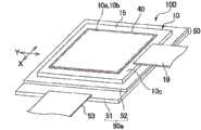
图1是示意地表示使用本发明的带输入装置的显示装置的构成的说明图。FIG. 1 is an explanatory diagram schematically showing the configuration of a display device with an input device using the present invention.
图2是示意地表示使用本发明的带输入装置的显示装置的俯视构成的说明图。FIG. 2 is an explanatory diagram schematically showing a plan view configuration of a display device with an input device using the present invention.
图3(a)、(b)、(c)分别是表示应用本发明的输入装置中所形成的透光性电极图形的俯视构成的说明图、示意表示将该输入装置在与A2-A2′线相应的位置处剖开时的状况的剖面图以及表示透光性电极图形和金属布线的连接结构的剖面图。Fig. 3 (a), (b), (c) are respectively the explanatory diagrams showing the top view structure of the translucent electrode pattern formed in the input device to which the present invention is applied, and schematically show that the input device is at A2-A2' A cross-sectional view showing the state when cut at the position corresponding to the line, and a cross-sectional view showing the connection structure of the light-transmitting electrode pattern and the metal wiring.
图4是表示使用本发明的输入装置中所形成的第1布线的构成例的说明图。FIG. 4 is an explanatory diagram showing a configuration example of a first wiring formed in the input device according to the present invention.
图5是表示本发明的参考例所涉及的输入装置中所形成的第1布线的构成例的说明图。5 is an explanatory diagram showing a configuration example of a first wiring formed in an input device according to a reference example of the present invention.
图6是表示应用本发明的输入装置中所形成的第2布线的构成例的说明图。FIG. 6 is an explanatory diagram showing a configuration example of a second wiring formed in the input device to which the present invention is applied.
图7是表示本发明的参考例所涉及的输入装置中所形成的第2布线的构成例的说明图。7 is an explanatory diagram showing a configuration example of a second wiring formed in the input device according to the reference example of the present invention.
图8(a)、(b)、(c)是使用本发明所涉及的带输入装置的显示装置的电子设备的说明图。8( a ), ( b ), and ( c ) are explanatory diagrams of electronic equipment using the display device with input device according to the present invention.
图9是示意地表示本发明的参考例所涉及的带输入装置的显示装置的俯视构成的说明图。9 is an explanatory diagram schematically showing a plan view configuration of a display device with an input device according to a reference example of the present invention.
符号说明Symbol Description
10··输入装置,10a··输入区域,10e··周边区域,11··第1透光性电极图形,12··第2透光性电极图形,15··透光性基板,11a、12a··垫状部(大面积部分),50··液晶装置(图像生成装置),100··带输入装置的显示装置,101a··第1输入区域,102a··第2输入区域,911~919··第1布线,921~926、929··第2布线,950··第1信号输入输出区域,955··第1布线区域,960··第2信号输入输出区域,961··近距离第2布线区域(第2布线的布线区域),962··远距离第2布线区域(第2布线的布线区域),971··第1辅助布线,972··第2辅助布线10...input device, 10a...input area, 10e...surrounding area, 11...first light-transmitting electrode pattern, 12...second light-transmitting electrode pattern, 15...light-transmitting substrate, 11a, 12a...pad-like portion (large area), 50...liquid crystal device (image generating device), 100...display device with input device, 101a...first input area, 102a...second input area, 911 ~919··First wiring, 921~926, 929··Second wiring, 950··First signal input and output area, 955··First wiring area, 960··Second signal input and output area, 961·· Short-distance second wiring area (wiring area of second wiring), 962··long-distance second wiring area (wiring area of second wiring), 971··first auxiliary wiring, 972··second auxiliary wiring
具体实施方式Detailed ways
参照附图,来说明本发明的实施方式。还有,在下面的说明中参照的附图内,为了将各层和各部件设为可在附图上辨认的程度的大小,所以按各层、各部件的每个都使比例尺不同。Embodiments of the present invention will be described with reference to the drawings. In addition, in the drawings referred to in the following description, in order to make each layer and each member a size that can be seen on the drawings, the scale is different for each layer and each member.
(整体构成)(overall composition)
图1及图2分别是示意表示应用本发明的带输入功能的显示装置的构成的说明图,以及示意表示该带输入装置的显示装置的俯视构成的说明图。还有,在图2中,减少了第1透光性电极图形及第2透光性电极图形、布线的数目等,进行表示。1 and 2 are explanatory diagrams schematically showing the configuration of a display device with an input function to which the present invention is applied, and explanatory diagrams schematically showing a plan view of the display device with an input device. In addition, in FIG. 2, the first light-transmitting electrode pattern and the second light-transmitting electrode pattern, the number of wiring lines, etc. are reduced and shown.
在图1中,本方式的带输入功能的显示装置100大体具有:作为图像生成装置的液晶装置50;和面板状的输入装置10(触摸面板),在该图像生成装置上重叠配置于出射显示光一侧的面上。液晶装置50具备透射型、反射型或者半透射反射型的有源矩阵型液晶面板50a,在透射型或者半透射反射型液晶面板的场合,在与显示光的出射侧相反一侧配置背光源装置(未图示)。另外,在液晶装置50中,对液晶面板50a重叠配置相位差板、偏振板(未图示)。液晶面板50a具备:元件基板51;对向基板52,对元件基板51对向配置;以及液晶层,被保持于对向基板52和元件基板51之间;在元件基板51,在从对向基板52的边缘伸出的区域连接柔性基板53。在元件基板51也有时以COG的方式安装驱动用IC。在任一场合下,液晶装置50都能够显示动态图像、静止图像,当进行对输入装置10的输入时,显示与输入信息对应的指示图像。从而,利用者只要用手指接触输入装置10所显示的指示图像,就可以进行信息的输入。In FIG. 1 , a
输入装置10是一种静电电容式的触摸面板,具备:透光性基板15;透光性的罩盖基板40,通过下述的粘接剂层(透光性树脂层)贴合于该透光性基板15;以及柔性基板19,连接于透光性基板15的端部。在柔性基板19上,连接着用来在输入装置10中执行输入位置检测的驱动电路(未图示),柔性基板19和透光性基板15的连接区域为下述的信号输入输出区域。在输入装置10中,由罩盖基板40的上表面构成输入面10b,罩盖基板40的大致中央区域成为被执行利用指尖实现的输入的输入区域10a。The
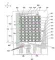
如图2所示,在透光性基板15的输入面10b侧的面之中的与输入区域10a相应的区域,形成:多列第1透光性电极图形11,按用箭头X所示的第1方向延伸;和多列第2透光性电极图形12,按用箭头Y所示的与第1方向交叉的第2方向延伸。As shown in Figure 2, in the area corresponding to the
在这种构成的输入装置10中,由于当对多个第1透光性电极图形11及多个第2透光性电极图形12依次施加电压、供给了电荷时,若作为导电体的手指接触输入区域10a内的某个部位,则在第1透光性电极图形11及第2透光性电极图形12、和手指之间也具有电容,作为其结果是使静电电容下降,因而可以检测出手指接触了哪个部位。In the
(输入区域的构成)(Structure of input area)
图3(a)、(b)、(c)分别是表示应用本发明的输入装置中所形成的透光性电极图形的俯视构成的说明图、示意表示将该输入装置在相当于A2-A2′线的位置处剖开后的状况的剖面图以及表示透光性电极图形和金属布线的连接结构的剖面图。还有,在图3(a)中,摘要表示了第1透光性电极图形及第2透光性电极图形的一部分。3(a), (b), and (c) are explanatory diagrams showing the top view of the translucent electrode pattern formed in the input device to which the present invention is applied, and schematically show that the input device is in a position corresponding to A2-A2 ′ and a cross-sectional view showing the connection structure between the light-transmitting electrode pattern and the metal wiring. In addition, in FIG. 3(a), part of the first light-transmitting electrode pattern and the second light-transmitting electrode pattern are schematically shown.
如图1、图2及图3(a)、(b)所示,在本方式的输入装置10中,第1透光性电极图形11和第2透光性电极图形12在透光性基板15的同一面上由同一层形成。另外,因为在输入区域10a,第1透光性电极图形11和第2透光性电极图形12在透光性基板15的同一面上由同一层形成,所以第1透光性电极图形11和第2透光性电极图形12的交叉部分18存在多个。因此,在本方式中,在多个交叉部分18的任一个中其构成都是:第1透光性电极图形11及第2透光性电极图形12之中的一方的电极图形在交叉部分18处也是相连的,另一方面,另一方的电极图形断开。在本方式中,在多个交叉部分18的任一个中其构成都是:第1透光性电极图形11相连,另一方面,第2透光性电极图形12断开。另外,在第1透光性电极图形11及第2透光性电极图形12的上层侧,透光性的层间绝缘膜4b形成于输入区域10a大致整体以及输入区域10a外侧的周边区域10e,在该层间绝缘膜4b的上层形成透光性的中继电极5a,其通过层间绝缘膜4b的接触孔4c,电连接在交叉部分18处断开的第2透光性电极图形12之间。因此,第2透光性电极图形12在Y方向上被电连接。As shown in Fig. 1, Fig. 2 and Fig. 3 (a), (b), in the
第1透光性电极图形11及第2透光性电极图形12分别在由交叉部分18所夹着的区域具备菱形形状的大面积垫状(pad)部11a、12a(大面积部分),在第1透光性电极图形11中位于交叉部分18的连接部分11c为与垫状部11a相比宽度较窄的窄幅形状。另外,中继电极5a也按与垫状部11a、12a相比宽度较窄的窄幅形状形成为长方形状。The first light-transmitting electrode pattern 11 and the second light-transmitting
在按上述方法构成的透光性基板15中,在形成第1透光性电极图形11及第2透光性电极图形12一侧的面上,在输入区域10a通过粘接剂层30粘贴透光性的罩盖基板40。In the
另外,在透光性基板15上,在输入区域10a的外侧区域(周边区域10e),形成与第1透光性电极图形11及第2透光性电极图形12的各自电连接的多条金属布线9a,这些金属布线9a的端部构成了用来连接柔性基板19的端子19a。这些金属布线9a构成将参照图2在下面说明的第1布线911~919及第2布线921~926、929。In addition, on the
在按上述方法构成的输入装置10中,在本方式中,因为形成第1透光性电极图形11及第2透光性电极图形12的区域与未形成第1透光性电极图形11及第2透光性电极图形12的区域的反射率之差,所以看得见第1透光性电极图形11及第2透光性电极图形12的存在,使美观度下降。因此,在本方式中,以防止该美观度的下降为目的,根据利用光学干涉的防止反射技术,设定第1透光性电极图形11及第2透光性电极图形12的材质及厚度。所谓利用光学干涉的防止反射技术指的是,当入射光由薄膜的表面、以及基板与薄膜的界面反射时,通过使该表面反射光与界面反射光的相位逆转将其相互抵消来减少反射光的技术。也就是说,在空气层的折射率(n0)、薄膜的折射率(n1)与膜厚(d1)、和基板的折射率(n2)满足下式In the
(n1)2=n0×n2(n1)2=n0×n2
n1×d1=λ/4n1×d1=λ/4
时,波长λ(nm)时的反射率为0%。如果利用这种防止反射技术,就可以消除:形成第1透光性电极图形11及第2透光性电极图形12的区域与未形成第1透光性电极图形11及第2透光性电极图形12的区域的反射率之差,而看不见第1透光性电极图形11及第2透光性电极图形12的存在。因此,在本方式中,采用ITO膜3a来形成第1透光性电极图形11和第2透光性电极图形12,在第1透光性电极图形11与透光性基板15的层间以及第2透光性电极图形12与透光性基板15的层间,形成用来实现防止反射结构的多层膜20。作为该多层膜20,例如可以使用ITO膜1a和氧化硅膜2a的叠层膜等。还有,第1透光性电极图形11及第2透光性电极图形12也有时采用IZO(Indium Zinc Oxide,氧化铟锌)膜来形成。, the reflectance at the wavelength λ (nm) is 0%. If this anti-reflection technology is utilized, it is possible to eliminate: the area where the first translucent electrode pattern 11 and the second
(布线的引绕结构)(Wiring routing structure)
还是在图2中,在本方式中,在透光性基板15上,在输入区域10a外侧的周边区域10e,形成从多个第1透光性电极图形11延伸的多条第1布线911~919相互并排延伸到第1信号输入输出区域950的第1布线区域955。第1信号输入输出区域950相对输入区域10a配置于Y方向上的一侧,第1布线区域955一边在多个部位处弯曲,一边从输入区域10a的X方向的一方端边10s沿着端边10s地延伸到第1信号输入输出区域950。因此,在本方式中,第1布线区域955(第1布线911~919)在周边区域10e具有:部位955d,从第1透光性电极图形11按X方向直线延伸;部位955c,从部位955d沿着输入区域10a的端边10s地按Y方向折弯成直角地进行延伸;部位955b,从部位955c朝向由第1信号输入输出区域950和输入区域10a所夹着的区域按X方向折弯成直角;以及部位955a,从部位955b朝向第1信号输入输出区域950按Y方向折弯成直角。Also in FIG. 2 , in this form, a plurality of
另外,在透光性基板15上,在输入区域10a外侧的周边区域10e,从多个第2透光性电极图形12延伸的多条第2布线921~926、929延伸到第2信号输入输出区域960。第2信号输入输出区域960也和第1信号输入输出区域950相同,相对输入区域10a配置于Y方向的一侧,第2信号输入输出区域960和第1信号输入输出区域950沿着透光性基板15的基板边排列成直线状。In addition, on the
在这里,输入区域10a被分割为:在Y方向上位于第2信号输入输出区域960侧的第1输入区域101a和在Y方向上位于与第2信号输入输出区域960侧相反一侧的第2输入区域102a,与之相对应,第2透光性电极图形12也在第1输入区域101a和第2输入区域102a之间被分割。因此,从多个第2透光性电极图形12延伸的布线的布线区域(第2布线区域)被分割成2个,对于该布线区域之中的、从第1输入区域101a朝向第2信号输入输出区域960延伸的第2布线929并排的近距离第2布线区域961,第2布线929之间以大致相等的长度尺寸空出足够的间隔进行延伸。因此,对于第2布线929而言,即使布线电阻及寄生电容不一致,也由于其自身程度(level)较低,因而没有影响。Here, the
与之相对,从第2输入区域102a朝向第2信号输入输出区域960延伸的远距离第2布线区域962,从相对输入区域10a位于与第2信号输入输出区域960侧相反一侧的端边10t,一边在多个部位处弯曲,一边沿着输入区域10a的X方向上的与端边10s相反一侧的端边10u地边弯曲边延伸到第2信号输入输出区域960。因此,在本方式中,远距离第2布线区域962(第2布线921~926)具有:部位962e,在第2透光性电极图形12的延长线上从输入区域10a的端边10t按Y方向直线延伸;部位962d,从部位962e平行于端边10t地按X方向延伸;部位962c,从部位962d沿着输入区域10a的端边10u地按Y方向折弯成直角而进行延伸;部位962b,从部位962c朝向由第2信号输入输出区域960和输入区域10a所夹着的区域按X方向折弯成直角;以及部位962a,从部位962b朝向第2信号输入输出区域960按Y方向折弯成直角。On the other hand, the long-distance
(寄生电容及布线电阻的不一致的应对措施)(Measures against inconsistencies in parasitic capacitance and wiring resistance)
如同参照图2所说明的那样,因为第1布线区域955从输入区域10a的X方向上的一方端边10s沿着端边10s地延伸到第1信号输入输出区域950,所以在第1布线区域955,各第1布线911~919的长度尺寸相差较大,且布线之间接近。因此,在该构成的原状下,在多条第1布线911~919中,寄生于其和相邻的布线之间的电容、布线电阻按每条布线相差较大。另外,对于第1布线911~919之中的、位于布线排列方向(第1布线区域955的宽度方向)的两端部的第1布线911、919来说,因为只在单侧存在相邻的布线,所以寄生电容较小。As described with reference to FIG. 2, since the
另外,远距离第2布线区域962从输入区域10a的端边10t沿着端边10u地延伸到第2信号输入输出区域960,在该远距离第2布线区域962中,各第2布线921~926的长度尺寸相差较大,且布线之间接近。因此,在该构成的原状下,在多条第2布线921~926中,寄生于其和相邻的布线之间的电容、布线电阻按每条布线相差较大。另外,对于第2布线921~926之中的、位于布线排列方向(远距离第2布线区域962的宽度方向)的外侧端部(离输入区域10a远的一侧端部)的第2布线926来说,因为只在单侧存在相邻的布线,所以寄生电容较小。还有,因为第2布线921~926之中的位于内侧端部(离输入区域10a近的一侧端部)的第2布线921,与第1透光性电极图形11的被分割成三角形的垫状部分的底边部并排,所以具备与在远距离第2布线区域962宽度方向上的内侧通过的第2布线922~925接近的寄生电容。In addition, the long-distance
为了消除这种寄生电容的按每条布线的不一致,在本方式中,首先,沿着第1布线区域955的两个端部各自延伸出在其与在两个端部延伸的第1布线911、919之间生成寄生电容的第1辅助布线971及第2辅助布线972。这种第1辅助布线971及第2辅助布线972之中的第1辅助布线971,和第1布线区域955(第1布线911~919)相同,在周边区域10e具有:部位955d,按X方向直线延伸;部位955c,从部位955d沿着输入区域10a的端边10s地按Y方向弯曲成直角地进行延伸;部位955b,从部位955c朝向由第1信号输入输出区域950和输入区域10a所夹着的区域按X方向折弯成直角;以及部位955a,从部位955b朝向与第1信号输入输出区域950相邻的位置按Y方向折弯成直角。另外,第2辅助布线972也和第1布线区域955(第1布线911~919)相同,在周边区域10e具有:部位955d,按X方向直线延伸;部位955c,从部位955d按Y方向折弯成直角地沿着输入区域10a的端边10s地进行延伸;部位955b,从部位955c朝向由第1信号输入输出区域950和输入区域10a所夹着的区域按X方向折弯成直角;以及部位955a,从部位955b朝向与第1信号输入输出区域950相邻的位置按Y方向折弯成直角。In order to eliminate such inconsistency of parasitic capacitance for each wiring, in this form, first, first, along both ends of the
另外,在本方式中,在远距离第2布线区域962,也和第1布线区域955相同,沿着外侧的端部,延伸出在其与在该端部延伸的第2布线926之间生成寄生电容的第1辅助布线971。从而,第1辅助布线971和第2布线区域962(第2布线921~926)相同,具有:部位962e,按Y方向直线延伸;部位962d,从部位962e平行于端边10t按X方向延伸;部位962c,从部位962d按Y方向折弯成直角地沿着输入区域10a的端边10u地进行延伸;部位962b,从部位962c朝向由第2信号输入输出区域960和输入区域10a所夹着的区域按X方向折弯成直角;以及部位962a,从部位962b朝向第2信号输入输出区域960侧的方向按Y方向折弯成直角。In addition, in this embodiment, in the long-distance
这里,第1辅助布线971与第2辅助布线972相比,在离输入区域10a远的位置通过,构成了在外周侧包围输入区域10a的外周侧屏蔽线。另外,第2辅助布线972保持成和第1辅助布线971相同的电位,在本方式中,对第1辅助布线971及第2辅助布线972施加定电位(接地电位)。Here, the first
当形成该第1辅助布线971及第2辅助布线972时,具体而言,和第1布线911~919及第2布线921~926、929的形成同时,形成第1辅助布线971及第2辅助布线972,通过在第1信号输入输出区域950和第2信号输入输出区域960并排的端子,把第1辅助布线971及第2辅助布线972和外部进行连接,从外部对第1辅助布线971及第2辅助布线972施加接地电位。如果采用该构成,就可以利用图3(c)所示的金属布线9a,和第1布线911~917及第2布线921~926、929一起,形成第1辅助布线971及第2辅助布线972。从而,由于即使不增加新的工序,也可以形成第1辅助布线971及第2辅助布线972,因而能够使生产性得到提高。When the first
另外,当形成第1辅助布线971及第2辅助布线972时,也可以在与第1布线911~919及第2布线921~926、929不同的层形成第1辅助布线971及第2辅助布线972。例如图3(c)所示,也可以用层间绝缘膜4b覆盖第1布线911~919及第2布线921~926、929,并且在层间绝缘膜4b的上层形成第1辅助布线971及第2辅助布线972,对于在第1信号输入输出区域950及第2信号输入输出区域960并排的端子,通过层间绝缘膜4b的去除区域,来连接第1辅助布线971及第2辅助布线972。这种情况下,将第1辅助布线971及第2辅助布线972通过端子与外部进行连接,从外部施加接地电位即可。通过按上述方法来构成,则即便其形成为第1辅助布线971及第2辅助布线972、与第1布线911~919及第2布线921~926、929交叉,也不发生短路。因此可以实现将第1辅助布线971及第2辅助布线972相连的构成、第1辅助布线971整周包围输入区域10a外周侧的构成等。如果采用将第1辅助布线971及第2辅助布线972相连的构成,则具有可以减少用来对第1辅助布线971及第2辅助布线972施加接地电位的端子的个数等的优点。另外,如果采用第1辅助布线971整周包围输入区域10a外周侧的构成,则具有可以可靠防止噪声从外部进入输入区域10a这样的优点。In addition, when the first
另外,在本方式中,形成于第1布线区域955的第1布线911~919,其相邻的布线的间隔,在布线长度较长的布线中,与布线长度较短的布线相比,在长度方向的至少一部分上变宽。在本方式中,由于从位于外侧的第1布线911朝向位于内侧的布线按顺序使布线长度变短,因而在外侧相邻的布线之间的间隔与在内侧相邻的布线之间的间隔相比,在长度方向的至少一部分上变宽。另外,形成于第1布线区域955的第1布线911~919,在布线长度较长的布线中,与布线长度较短的布线相比,在长度方向的至少一部分上宽度尺寸变宽。在本方式中,由于从位于外侧的第1布线911朝向位于内侧的布线按顺序使布线长度变短,因而位于外侧的布线与位于内侧的布线相比,在长度方向的至少一部分上变宽。In addition, in this embodiment, the distance between the adjacent wirings of the
另外,形成于远距离第2布线区域962的第2布线921~926,其相邻的布线的间隔,在布线长度较长的布线中,与布线长度较短的布线相比,在长度方向的至少一部分上变宽。在本方式中,由于从位于内侧的第2布线921朝向位于外侧的布线按顺序使布线长度变长,因而在外侧相邻的布线之间的间隔与在内侧相邻的布线之间的间隔相比,在长度方向的至少一部分上变宽。另外,形成于远距离第2布线区域962的第2布线921~926在布线长度较长的布线中,与布线长度较短的布线相比,在长度方向的至少一部分宽度尺寸变宽。在本方式中,由于从位于内侧的第2布线921朝向位于外侧的布线按顺序使布线长度变长,因而位于外侧的布线与位于内侧的布线相比,在长度方向的至少一部分变宽。In addition, the distance between the adjacent wirings of the
(第1布线911~919的构成例)(Configuration example of the
根据该规则,参照图4及图5来说明构成第1布线911~919的例子的效果。Based on this rule, the effect of an example of configuring the
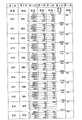
图4是表示应用本发明的输入装置10中所形成的第1布线911~919等的构成例的说明图。在图4中,在从左侧朝向右侧的第1栏、第2栏、第3栏、第4栏、第5栏、第6栏及第7栏中分别表示出图2所示的第1布线的标号、图2所示的部位、每个部位的长度尺寸、每个部位的宽度尺寸、与位于内侧的第1布线之间的间隔、寄生电容及布线电阻,在表示寄生电容的第6栏中,括号的数值是寄生于其与位于内侧的布线之间的电容的值。还有,第1布线911~919等的长度尺寸和宽度尺寸表示出图2所示的部位955a~955d的每一个的值。FIG. 4 is an explanatory diagram showing a configuration example of
图5是表示本发明的参考例所涉及的输入装置10中所形成的第1布线911~919的构成例的说明图,相当于在图2所示的构成中未形成第1辅助布线971及第2辅助布线972,而使全部的第1布线911~919的间隔相等的例子。还有,图5的第1~7栏分别对应于图4的第1~7栏。5 is an explanatory diagram showing a configuration example of the
还有,图4及图5所示的寄生电容是根据覆盖布线周围的绝缘层的介电常数、布线宽度、布线之间的间隔及布线之间的对向长度计算出的值。The parasitic capacitance shown in FIGS. 4 and 5 is a value calculated from the dielectric constant of the insulating layer covering the periphery of the wiring, the width of the wiring, the distance between the wirings, and the facing length between the wirings.
首先,如同从图4所判明的那样,在第1布线911~919中,对位于两侧的第1布线911、919形成第1辅助布线971及第2辅助布线972,且第1布线911和第1布线912的间隔在部位955b、955c处是55μm,与之相对,第1布线912和第1布线913的间隔在部位955b、955c处变成45μm等等,相邻的布线的间隔在布线长度较长的布线中与布线长度较短的布线相比、在长度方向的至少一部分上变宽。因此,寄生于第1布线911中的电容值作为第1辅助布线971和第1布线912的电容之和,是4.88pF,和寄生于其他的第1布线912~918中的电容值(4.83~5.04pF)等同。另外,寄生于第1布线919中的电容值作为第2辅助布线972和第1布线918的电容之和,是4.82pF,和寄生于其他的第1布线912~918中的电容值(4.83~5.04pF)等同。First, as is clear from FIG. 4 , among the
再者,在第1布线911~919中,在最长的第1布线911中宽度最狭窄的部位的尺寸是65μm,与之相对,在第1布线912中宽度最狭窄的部位的尺寸是60μm等,在布线长度较长的布线中与布线长度较短的布线相比,在长度方向的至少一部分上宽度尺寸变宽。因此,第1布线911的布线电阻是375Ω,和其他的第1布线912~919的电阻(389~531Ω)大致相等。该金属布线的表面电阻是0.2Ω/□。In addition, among the
与之相对,如同从图5所判明的那样,在不使用本发明的规则时,例如在任一条第1布线911~919中使布线间隔相等时,虽然寄生于第1布线911~919中的电容值产生较大不一致而为4.01~12.87pF,但是对于第1布线911~919的布线电阻,因为在本参考例中也调整了布线宽度,所以为233~307Ω而大致相等。On the other hand, as is clear from FIG. 5 , when the rules of the present invention are not used, for example, when the wiring intervals are made equal in any of the
还有,参照图4及图5所说明的构成归根结底是一例,也可以在不脱离本发明宗旨的范围内进行各种改变。In addition, the structure demonstrated with reference to FIG. 4 and FIG. 5 is an example after all, and various changes can be made in the range which does not deviate from the gist of this invention.
(第2布线921~926的构成例)(Configuration example of the
根据本发明所涉及的规则,参照图6及图7来说明构成第2布线921~926的例子的效果。Effects of an example of configuring the
图6是表示应用本发明的输入装置10中所形成的第2布线921~926等的构成例的说明图。在图6中,在从左侧朝向右侧的第1栏、第2栏、第3栏、第4栏、第5栏、第6栏及第7栏中分别表示出图2所示的第1布线的标号、图2所示的部位、每个部位的长度尺寸、每个部位的宽度尺寸、与位于内侧的第1布线之间的间隔、寄生电容及布线电阻,在表示寄生电容的第6栏中,括号的数值是寄生于其和位于外侧的布线之间的电容的值,附上*的数值是寄生于第2布线921和第1透光性电极图形11之间的电容的值。还有,第2布线921~926等的长度尺寸和宽度尺寸表示出图2所示的部位962a~962e的每一个的值。FIG. 6 is an explanatory diagram showing a configuration example of
图7是表示本发明的参考例所涉及的输入装置10中所形成的第2布线921~926的构成例的说明图,相当于在图2所示的构成中未形成第1辅助布线971及第2辅助布线972,而使全部的第2布线921~926的间隔相等的例子。还有,图7的第1~7栏分别对应于图6的第1~7栏。7 is an explanatory diagram showing a configuration example of the
还有,图6及图7所示的寄生电容是根据覆盖布线周围的绝缘层的介电常数、布线宽度、布线之间的间隔及布线之间的对向长度计算出的值。The parasitic capacitance shown in FIGS. 6 and 7 is a value calculated from the dielectric constant of the insulating layer covering the periphery of the wiring, the width of the wiring, the distance between the wirings, and the facing length between the wirings.
如同从图6所判明的那样,在第2布线921~926中,对位于最外侧的第2布线926形成第1辅助布线971,且第2布线926和第2布线925的间隔在部位962b、962c及962d处是50μm,与之相对,第2布线923和第2布线922的间隔在部位962b、962c及962d处变成45μm等等,相邻的布线的间隔在布线长度较长的布线中与布线长度较短的布线相比,在长度方向的至少一部分上变宽。因此,寄生于第2布线926中的电容值作为第1辅助布线971和第2布线925的电容之和,是6.22pF,和寄生于其他的第1布线922~925中的电容值(6.14~6.31pF)等同。另外,寄生于第2布线921中的电容值是4.68pF,若加入附上*的数值1.61pF(寄生于第2布线921和第1透光性电极图形11之间的电容的值),则变为6.29pF,和寄生于其他的第2布线922~925中的电容值(6.14~6.31pF)等同。6, among the
再者,在第2布线921~926中,在最长的第2布线926中宽度最狭窄的部位的尺寸是70μm,与之相对,在第2布线922中宽度最狭窄的部位的尺寸是65μm等等,在布线长度较长的布线中与布线长度较短的布线相比,在长度方向的至少一部分上宽度尺寸变宽。因此,第2布线926的布线电阻是511Ω,和其他的第2布线921~925的电阻(418~484Ω)大致相等。Furthermore, among the
与之相对,如同从图7所判明的那样,在不使用本发明的规则时,虽然寄生于第2布线921~926中的电容值产生较大不一致而为9.41~20.62pF,但是对于第2布线921~926的布线电阻,因为在本参考例中也调整了布线宽度,所以大致相等而为376~426Ω。On the other hand, as can be seen from FIG. 7, when the rules of the present invention are not used, although the capacitance values parasitic in the
还有,参照图6及图7所说明的构成归根结底是一例,也可以在不脱离本发明宗旨的范围内进行各种改变。In addition, the structure demonstrated with reference to FIG. 6 and FIG. 7 is an example after all, and various changes can be made in the range which does not deviate from the gist of this invention.
(本方式的主要效果)(The main effect of this method)
如同上面所说明的那样,对于第1布线区域955、远距离第2布线区域962端部的布线,因为只在单侧存在相邻的布线,所以存在寄生电容变小的趋势,但是在本方式中,因为使第1辅助布线971及第2辅助布线972沿着第1布线区域955、远距离第2布线区域962的端部地延伸,所以在端部的布线中,也寄生有与其他布线相同的电容。为此,因为寄生于多条布线各自中的电容相等,所以能够正确检测电容变化,可以使检测灵敏度得到提高。As explained above, for the wiring at the end of the
而且,因为由第1辅助布线971构成在外周侧包围输入区域10a的屏蔽线,所以能够防止从外部进入的噪声的影响,因此可以正确检测电容变化,能够使检测灵敏度得到提高。Furthermore, since the first
再者,因为根据布线长度的长短使相邻的布线间隔、布线宽度合理化,所以寄生于多条布线各自中的电容、布线电阻相等。故,可以正确检测电容变化,能够使检测灵敏度得到提高。In addition, since the interval between adjacent wirings and the wiring width are rationalized according to the length of the wiring, the capacitance and wiring resistance parasitic in each of the plurality of wirings are equal. Therefore, the capacitance change can be accurately detected, and the detection sensitivity can be improved.
[其他的实施方式][other embodiments]
在上述方式中,虽然使用了作为图像生成装置的液晶装置50,但是也可以使用有机电致发光装置或等离子体显示装置,来作为图像生成装置。In the above embodiment, although the
另外,在上述方式中,虽然在远距离第2布线区域962只设置了第1辅助布线971,但是也可以根据布局等的不同,在远距离第2布线区域962的内周侧还设置第2辅助布线972。In addition, in the above method, although only the first
另外,在上述方式中,虽然是分割了输入区域10a的例子,但是在输入区域10a未被分割的情况下,也可以在布线间在寄生电容、布线电阻方面存在不一致时使用本发明。In addition, although the above embodiment is an example where the
[对电子设备的装载例][loading example to electronic equipment]
下面,对于使用上述实施方式所涉及的带输入功能的显示装置100的电子设备,进行说明。图8(a)表示具备带输入功能的显示装置100的便携式个人计算机的构成。个人计算机2000具备作为显示单元的带输入功能的显示装置100和主体部2010。在主体部2010,设置电源开关2001及键盘2002。图8(b)表示具备带输入功能的显示装置100的便携电话机的构成。便携电话机3000具备多个操作按键3001、滚动按钮3002及作为显示单元的带输入功能的显示装置100。通过操作滚动按钮3002,使显示于带输入功能的显示装置100的画面滚动。图8(c)表示使用带输入功能的显示装置100的信息便携终端(PDA:Personal Digital Assistants,个人数字助理)的构成。信息便携终端4000具备多个操作按键4001、电源开关4002及作为显示单元的带输入功能的显示装置100。若操作了电源开关4002,则地址录、日程本之类的各种信息显示于带输入功能的显示装置100。Next, an electronic device using the display device with
还有,作为使用带输入功能的显示装置100的电子设备,除了图8所示的设备之外,还能举出数字静止相机、液晶电视机、汽车导航装置、寻呼机、电子记事本、台式电子计算器、文字处理机、工作站、电视电话机、POS终端等的终端设备等等。In addition, as electronic equipment using the
Claims (3)
Translated fromChineseApplications Claiming Priority (2)
| Application Number | Priority Date | Filing Date | Title |
|---|---|---|---|
| JP079906/08 | 2008-03-26 | ||
| JP2008079906AJP4582169B2 (en) | 2008-03-26 | 2008-03-26 | Capacitance type input device, display device with input function, and electronic device |
Related Parent Applications (1)
| Application Number | Title | Priority Date | Filing Date |
|---|---|---|---|
| CN2009101297616ADivisionCN101546243B (en) | 2008-03-26 | 2009-03-26 | Capacitive input device, display device with input function, and electronic equipment |
Publications (2)
| Publication Number | Publication Date |
|---|---|
| CN102087568A CN102087568A (en) | 2011-06-08 |
| CN102087568Btrue CN102087568B (en) | 2013-11-13 |
Family
ID=41116376
Family Applications (2)
| Application Number | Title | Priority Date | Filing Date |
|---|---|---|---|
| CN2009101297616AExpired - Fee RelatedCN101546243B (en) | 2008-03-26 | 2009-03-26 | Capacitive input device, display device with input function, and electronic equipment |
| CN2011100691449AExpired - Fee RelatedCN102087568B (en) | 2008-03-26 | 2009-03-26 | Electrical capacitance input device, display apparatus with input function and electronic apparatus |
Family Applications Before (1)
| Application Number | Title | Priority Date | Filing Date |
|---|---|---|---|
| CN2009101297616AExpired - Fee RelatedCN101546243B (en) | 2008-03-26 | 2009-03-26 | Capacitive input device, display device with input function, and electronic equipment |
Country Status (5)
| Country | Link |
|---|---|
| US (1) | US8531409B2 (en) |
| JP (1) | JP4582169B2 (en) |
| KR (1) | KR101031120B1 (en) |
| CN (2) | CN101546243B (en) |
| TW (1) | TWI407353B (en) |
Families Citing this family (67)
| Publication number | Priority date | Publication date | Assignee | Title |
|---|---|---|---|---|
| JP5103254B2 (en) | 2008-04-16 | 2012-12-19 | 株式会社ジャパンディスプレイイースト | Capacitive touch panel and screen input type display device including the same |
| JP2009265748A (en)* | 2008-04-22 | 2009-11-12 | Hitachi Displays Ltd | Display with touch panel |
| JP5033078B2 (en)* | 2008-08-06 | 2012-09-26 | 株式会社ジャパンディスプレイイースト | Display device |
| JP2010108222A (en)* | 2008-10-30 | 2010-05-13 | Kyocera Corp | Touch panel and touch panel type display device |
| JP5113773B2 (en)* | 2009-01-20 | 2013-01-09 | 株式会社ジャパンディスプレイイースト | Display device |
| JP5106471B2 (en)* | 2009-04-24 | 2012-12-26 | 三菱電機株式会社 | Touch panel and display device including the same |
| KR101082607B1 (en)* | 2009-10-16 | 2011-11-10 | 엘지이노텍 주식회사 | Planer member for touch panel and method for manufacturing same |
| KR101611906B1 (en)* | 2009-10-27 | 2016-04-14 | 엘지디스플레이 주식회사 | Stereoscopic Liquid Crystal Display Device Having Touch Panel and Method for Manufacturing the Same |
| JP5537915B2 (en) | 2009-12-01 | 2014-07-02 | 株式会社ジャパンディスプレイ | Touch panel |
| JP2011128674A (en)* | 2009-12-15 | 2011-06-30 | Sony Corp | Electrostatic capacitance-type input device and method for manufacturing the same |
| KR101073215B1 (en)* | 2010-03-05 | 2011-10-12 | 삼성모바일디스플레이주식회사 | flat panel display integrated touch screen panel |
| TWI471798B (en)* | 2010-03-12 | 2015-02-01 | Alps Electric Co Ltd | Input device |
| JP5520093B2 (en)* | 2010-03-16 | 2014-06-11 | 株式会社ジャパンディスプレイ | Manufacturing method of touch panel |
| KR101101053B1 (en)* | 2010-03-16 | 2011-12-29 | 삼성모바일디스플레이주식회사 | Touch screen panel and its manufacturing method |
| CN102200866B (en)* | 2010-03-24 | 2015-11-25 | 上海天马微电子有限公司 | Mutual capacitance touch sensing device, detection method thereof and touch display device |
| US8363034B2 (en) | 2010-04-14 | 2013-01-29 | Panasonic Corporation | Touch panel device |
| CN102221945B (en)* | 2010-04-14 | 2015-06-10 | 上海天马微电子有限公司 | Touch screen, liquid crystal display and drive detection method |
| TWI420362B (en) | 2010-04-19 | 2013-12-21 | Au Optronics Corp | Touch panel |
| CN101882021A (en)* | 2010-06-08 | 2010-11-10 | 苏州瀚瑞微电子有限公司 | Touch pad layout method |
| KR101333000B1 (en)* | 2010-07-22 | 2013-11-25 | 알프스 덴키 가부시키가이샤 | Input device and method of manufacturing the same |
| US20120026123A1 (en)* | 2010-07-30 | 2012-02-02 | Grunthaner Martin Paul | Compensation for Capacitance Change in Touch Sensing Device |
| KR101323052B1 (en)* | 2010-10-01 | 2013-10-29 | 엘지디스플레이 주식회사 | Electrostatic capacity type touch screen panel |
| KR101323004B1 (en)* | 2010-10-01 | 2013-10-29 | 엘지디스플레이 주식회사 | Capacity type touch screen panel |
| KR101323033B1 (en)* | 2010-10-20 | 2013-10-29 | 엘지디스플레이 주식회사 | Electrostatic capacity type touch screen panel |
| JP5730551B2 (en) | 2010-12-01 | 2015-06-10 | 株式会社ワコム | Detection sensor for detecting an indication position by an indicator, an indicator position detection device, and a method for manufacturing the detection sensor |
| EP3521986B1 (en)* | 2011-01-19 | 2020-05-20 | Lg Innotek Co. Ltd | Touch panel |
| KR101908492B1 (en) | 2011-04-12 | 2018-10-17 | 엘지디스플레이 주식회사 | Display device associated with touch panel |
| JP2012238066A (en)* | 2011-05-10 | 2012-12-06 | Japan Display East Co Ltd | Capacitive touch panel and display device |
| KR101868473B1 (en)* | 2011-08-11 | 2018-06-19 | 엘지디스플레이 주식회사 | Display Device Integrated with Touch Screen |
| KR101475106B1 (en)* | 2011-08-23 | 2014-12-23 | 엘지디스플레이 주식회사 | Electrostatic capacity type touch screen panel and method of manufacturing the same |
| US9259904B2 (en)* | 2011-10-20 | 2016-02-16 | Apple Inc. | Opaque thin film passivation |
| KR101197460B1 (en)* | 2012-01-27 | 2012-11-12 | 크루셜텍 (주) | Touch detection apparatus and method for reducing parasitic capacitance |
| JP5865819B2 (en)* | 2012-02-10 | 2016-02-17 | アルプス電気株式会社 | Input device |
| US20150062458A1 (en)* | 2012-03-29 | 2015-03-05 | Kyocera Corporation | Input device, display device, and electronic device |
| JP5876351B2 (en)* | 2012-03-29 | 2016-03-02 | 三菱製紙株式会社 | Light transmissive electrode |
| JP6029842B2 (en)* | 2012-03-30 | 2016-11-24 | アルプス電気株式会社 | Capacitive input device |
| JP6032794B2 (en)* | 2012-06-08 | 2016-11-30 | 株式会社ジャパンディスプレイ | Liquid crystal display |
| KR101968929B1 (en)* | 2012-09-11 | 2019-04-16 | 삼성디스플레이 주식회사 | Sensor substrate, method of manufacturing the same and sensing display panel having the same |
| KR101628724B1 (en)* | 2012-11-13 | 2016-06-09 | 엘지디스플레이 주식회사 | Display device with integrated touch screen |
| JP2014102747A (en)* | 2012-11-21 | 2014-06-05 | Panasonic Liquid Crystal Display Co Ltd | Touch panel device and control method of touch panel device |
| US9379704B2 (en)* | 2012-12-24 | 2016-06-28 | Htc Corporation | Touch panel |
| JP5722954B2 (en)* | 2013-06-23 | 2015-05-27 | 日本写真印刷株式会社 | Touch panel with pressure detection function |
| KR102037515B1 (en)* | 2013-08-29 | 2019-10-28 | 엘지디스플레이 주식회사 | Electrostatic capacitive type touch-sensitive panel for display device |
| JP6037039B2 (en)* | 2013-10-08 | 2016-11-30 | 株式会社村田製作所 | Tactile presentation device |
| KR102211863B1 (en)* | 2013-10-15 | 2021-02-04 | 삼성디스플레이 주식회사 | Touch panel and method of manufacturing a touch panel |
| JP6502012B2 (en)* | 2013-11-22 | 2019-04-17 | 株式会社Vtsタッチセンサー | Transparent conductive laminate, touch panel, and display device |
| CN104750888A (en)* | 2013-12-30 | 2015-07-01 | 北京华大九天软件有限公司 | Wiring method for connecting two groups of vertical ports in orthogonal equal width mode in layout |
| CN103970393A (en)* | 2014-05-23 | 2014-08-06 | 山东华芯富创电子科技有限公司 | Bridging capacitive touch panel structure and fabrication method for same |
| CN106462286A (en)* | 2014-06-12 | 2017-02-22 | 三菱制纸株式会社 | Light-transmitting electrically-conductive material |
| JP2016009213A (en)* | 2014-06-20 | 2016-01-18 | ホシデン株式会社 | Capacitive touch panel |
| TWI615749B (en)* | 2014-11-28 | 2018-02-21 | Sharp Kk | Display device with position input function |
| WO2016117841A2 (en)* | 2015-01-21 | 2016-07-28 | 엘지이노텍 주식회사 | Touch window |
| JP2016162305A (en)* | 2015-03-03 | 2016-09-05 | 日本航空電子工業株式会社 | Touch panel and method for manufacturing the same |
| JP6456230B2 (en)* | 2015-04-21 | 2019-01-23 | 三菱電機株式会社 | Touch screen, touch panel, display device and electronic device |
| JP6562706B2 (en)* | 2015-05-13 | 2019-08-21 | 三菱電機株式会社 | Surface device, touch screen and liquid crystal display device |
| JP5981005B2 (en)* | 2015-09-02 | 2016-08-31 | 株式会社ジャパンディスプレイ | Display device |
| CN105446533B (en)* | 2015-11-19 | 2018-08-31 | 业成光电(深圳)有限公司 | The line construction of touch panel |
| CN106066740B (en) | 2016-08-02 | 2019-02-12 | 厦门天马微电子有限公司 | Touch-control display panel and touch control display apparatus |
| JP6240278B2 (en)* | 2016-08-10 | 2017-11-29 | 株式会社ジャパンディスプレイ | LCD with built-in touch panel |
| WO2018143412A1 (en)* | 2017-02-06 | 2018-08-09 | シャープ株式会社 | Display device |
| KR102354247B1 (en) | 2017-04-24 | 2022-01-24 | 삼성디스플레이 주식회사 | Display module |
| KR102421927B1 (en)* | 2017-06-01 | 2022-07-18 | 엘지디스플레이 주식회사 | Touch display device |
| WO2019114913A2 (en)* | 2017-12-14 | 2019-06-20 | محمد أحمد الجميل، | Energy recovery in capacitor devices that operate repeatedly |
| KR102502274B1 (en)* | 2018-02-21 | 2023-02-22 | 삼성디스플레이 주식회사 | Display apparatus |
| KR102150881B1 (en) | 2019-03-21 | 2020-09-02 | 동우 화인켐 주식회사 | Touch Sensor and Stepper Mask for Fabricating the Same |
| JP7331160B2 (en)* | 2020-09-02 | 2023-08-22 | 株式会社ジャパンディスプレイ | Display device |
| JP2024030142A (en) | 2022-08-23 | 2024-03-07 | シャープディスプレイテクノロジー株式会社 | Electrostatic capacitive touch panel |
Citations (1)
| Publication number | Priority date | Publication date | Assignee | Title |
|---|---|---|---|---|
| CN1955904A (en)* | 2005-10-27 | 2007-05-02 | 阿尔卑斯电气株式会社 | Input device and electric device using the same |
Family Cites Families (13)
| Publication number | Priority date | Publication date | Assignee | Title |
|---|---|---|---|---|
| JPS6075927A (en) | 1983-09-30 | 1985-04-30 | Fujitsu Ltd | Coordinate input device |
| JPH02140934A (en)* | 1988-11-21 | 1990-05-30 | Nec Corp | Semiconductor device |
| JP2674462B2 (en)* | 1993-04-13 | 1997-11-12 | 日本電気株式会社 | Semiconductor device |
| JP2002237188A (en)* | 2001-02-13 | 2002-08-23 | Mitsubishi Electric Corp | Semiconductor storage device |
| JP2004030086A (en)* | 2002-06-25 | 2004-01-29 | Matsushita Electric Ind Co Ltd | Design method of semiconductor integrated circuit |
| JP4435622B2 (en)* | 2004-05-25 | 2010-03-24 | アルプス電気株式会社 | Capacitance type detection device |
| TWI271645B (en)* | 2005-04-19 | 2007-01-21 | Elan Microelectronics Corp | Capacitive touchpad with a physical key function |
| JP2007018226A (en)* | 2005-07-07 | 2007-01-25 | Three M Innovative Properties Co | Touch panel sensor |
| GB2428306B (en)* | 2005-07-08 | 2007-09-26 | Harald Philipp | Two-dimensional capacitive position sensor |
| JP2007184125A (en)* | 2006-01-05 | 2007-07-19 | Seiko Epson Corp | Light emitting device and image printing device |
| US20070268272A1 (en)* | 2006-05-19 | 2007-11-22 | N-Trig Ltd. | Variable capacitor array |
| US20080047764A1 (en)* | 2006-08-28 | 2008-02-28 | Cypress Semiconductor Corporation | Temperature compensation method for capacitive sensors |
| JP5380723B2 (en)* | 2007-08-07 | 2014-01-08 | Nltテクノロジー株式会社 | Surface display device and electronic device |
- 2008
- 2008-03-26JPJP2008079906Apatent/JP4582169B2/ennot_activeExpired - Fee Related
- 2009
- 2009-02-24USUS12/391,322patent/US8531409B2/ennot_activeExpired - Fee Related
- 2009-03-23TWTW098109337Apatent/TWI407353B/ennot_activeIP Right Cessation
- 2009-03-24KRKR1020090024808Apatent/KR101031120B1/ennot_activeExpired - Fee Related
- 2009-03-26CNCN2009101297616Apatent/CN101546243B/ennot_activeExpired - Fee Related
- 2009-03-26CNCN2011100691449Apatent/CN102087568B/ennot_activeExpired - Fee Related
Patent Citations (1)
| Publication number | Priority date | Publication date | Assignee | Title |
|---|---|---|---|---|
| CN1955904A (en)* | 2005-10-27 | 2007-05-02 | 阿尔卑斯电气株式会社 | Input device and electric device using the same |
Also Published As
| Publication number | Publication date |
|---|---|
| CN101546243A (en) | 2009-09-30 |
| TW200945157A (en) | 2009-11-01 |
| JP4582169B2 (en) | 2010-11-17 |
| JP2009237673A (en) | 2009-10-15 |
| CN101546243B (en) | 2011-09-21 |
| KR101031120B1 (en) | 2011-04-27 |
| TWI407353B (en) | 2013-09-01 |
| US20090244021A1 (en) | 2009-10-01 |
| US8531409B2 (en) | 2013-09-10 |
| CN102087568A (en) | 2011-06-08 |
| KR20090102663A (en) | 2009-09-30 |
Similar Documents
| Publication | Publication Date | Title |
|---|---|---|
| CN102087568B (en) | Electrical capacitance input device, display apparatus with input function and electronic apparatus | |
| JP4506785B2 (en) | Capacitive input device | |
| JP4720857B2 (en) | Capacitance type input device and display device with input function | |
| JP4888589B2 (en) | Capacitance type input device, display device with input function, and electronic device | |
| JP4998919B2 (en) | Capacitive input device | |
| JP5300640B2 (en) | Capacitance type input device and electro-optical device with input device | |
| US8872786B2 (en) | Capacitive input device, display device with input function, and electronic apparatus | |
| CN101910987B (en) | Display device, electronic device provided with the display device, and touch panel | |
| US9086766B2 (en) | Touch panel and touch display panel | |
| WO2010016174A1 (en) | Touch panel, display, and electronic device | |
| US20120019473A1 (en) | Systems for displaying images | |
| CN101414237A (en) | Touch panel, display device with input function, and electronic apparatus | |
| JP2009098834A (en) | Capacitance type input device, display device with input function and electronic equipment | |
| CN104850290A (en) | Touch sensor board, image display device, and touch sensor board manufacturing method | |
| CN103823588B (en) | Touch device and driving method thereof | |
| CN106648258B (en) | Array substrate, touch display panel and touch display device | |
| TWI453643B (en) | Touch panel and electronic device | |
| KR101323048B1 (en) | Electrostatic capacitive type touch-sensitive panel for display device | |
| CN102955623B (en) | Touch Panels and Electronics |
Legal Events
| Date | Code | Title | Description |
|---|---|---|---|
| C06 | Publication | ||
| PB01 | Publication | ||
| C10 | Entry into substantive examination | ||
| SE01 | Entry into force of request for substantive examination | ||
| ASS | Succession or assignment of patent right | Owner name:JAPAN DISPLAY WEST INC. Free format text:FORMER OWNER: SONY CORPORATION Effective date:20121107 | |
| C41 | Transfer of patent application or patent right or utility model | ||
| TA01 | Transfer of patent application right | Effective date of registration:20121107 Address after:Aichi Applicant after:Japan display West Co.,Ltd. Address before:Tokyo, Japan Applicant before:Sony Corp. | |
| C14 | Grant of patent or utility model | ||
| GR01 | Patent grant | ||
| CF01 | Termination of patent right due to non-payment of annual fee | Granted publication date:20131113 Termination date:20200326 | |
| CF01 | Termination of patent right due to non-payment of annual fee |