CN102083280A - Embedded printed circuit board, multi-layer printed circuit board and manufacturing method thereof - Google Patents
Embedded printed circuit board, multi-layer printed circuit board and manufacturing method thereofDownload PDFInfo
- Publication number
- CN102083280A CN102083280ACN2010105880175ACN201010588017ACN102083280ACN 102083280 ACN102083280 ACN 102083280ACN 2010105880175 ACN2010105880175 ACN 2010105880175ACN 201010588017 ACN201010588017 ACN 201010588017ACN 102083280 ACN102083280 ACN 102083280A
- Authority
- CN
- China
- Prior art keywords
- circuit pattern
- insulating layer
- layer
- pcb
- circuit board
- Prior art date
- Legal status (The legal status is an assumption and is not a legal conclusion. Google has not performed a legal analysis and makes no representation as to the accuracy of the status listed.)
- Granted
Links
Images


Classifications
- H—ELECTRICITY
- H05—ELECTRIC TECHNIQUES NOT OTHERWISE PROVIDED FOR
- H05K—PRINTED CIRCUITS; CASINGS OR CONSTRUCTIONAL DETAILS OF ELECTRIC APPARATUS; MANUFACTURE OF ASSEMBLAGES OF ELECTRICAL COMPONENTS
- H05K3/00—Apparatus or processes for manufacturing printed circuits
- H05K3/46—Manufacturing multilayer circuits
- H05K3/4644—Manufacturing multilayer circuits by building the multilayer layer by layer, i.e. build-up multilayer circuits
- H05K3/465—Manufacturing multilayer circuits by building the multilayer layer by layer, i.e. build-up multilayer circuits by applying an insulating layer having channels for the next circuit layer
- H—ELECTRICITY
- H05—ELECTRIC TECHNIQUES NOT OTHERWISE PROVIDED FOR
- H05K—PRINTED CIRCUITS; CASINGS OR CONSTRUCTIONAL DETAILS OF ELECTRIC APPARATUS; MANUFACTURE OF ASSEMBLAGES OF ELECTRICAL COMPONENTS
- H05K3/00—Apparatus or processes for manufacturing printed circuits
- H05K3/10—Apparatus or processes for manufacturing printed circuits in which conductive material is applied to the insulating support in such a manner as to form the desired conductive pattern
- H05K3/107—Apparatus or processes for manufacturing printed circuits in which conductive material is applied to the insulating support in such a manner as to form the desired conductive pattern by filling grooves in the support with conductive material
- H—ELECTRICITY
- H05—ELECTRIC TECHNIQUES NOT OTHERWISE PROVIDED FOR
- H05K—PRINTED CIRCUITS; CASINGS OR CONSTRUCTIONAL DETAILS OF ELECTRIC APPARATUS; MANUFACTURE OF ASSEMBLAGES OF ELECTRICAL COMPONENTS
- H05K3/00—Apparatus or processes for manufacturing printed circuits
- H05K3/10—Apparatus or processes for manufacturing printed circuits in which conductive material is applied to the insulating support in such a manner as to form the desired conductive pattern
- H05K3/18—Apparatus or processes for manufacturing printed circuits in which conductive material is applied to the insulating support in such a manner as to form the desired conductive pattern using precipitation techniques to apply the conductive material
- H05K3/181—Apparatus or processes for manufacturing printed circuits in which conductive material is applied to the insulating support in such a manner as to form the desired conductive pattern using precipitation techniques to apply the conductive material by electroless plating
- H05K3/182—Apparatus or processes for manufacturing printed circuits in which conductive material is applied to the insulating support in such a manner as to form the desired conductive pattern using precipitation techniques to apply the conductive material by electroless plating characterised by the patterning method
- H05K3/184—Apparatus or processes for manufacturing printed circuits in which conductive material is applied to the insulating support in such a manner as to form the desired conductive pattern using precipitation techniques to apply the conductive material by electroless plating characterised by the patterning method using masks
- H—ELECTRICITY
- H05—ELECTRIC TECHNIQUES NOT OTHERWISE PROVIDED FOR
- H05K—PRINTED CIRCUITS; CASINGS OR CONSTRUCTIONAL DETAILS OF ELECTRIC APPARATUS; MANUFACTURE OF ASSEMBLAGES OF ELECTRICAL COMPONENTS
- H05K3/00—Apparatus or processes for manufacturing printed circuits
- H05K3/10—Apparatus or processes for manufacturing printed circuits in which conductive material is applied to the insulating support in such a manner as to form the desired conductive pattern
- H05K3/20—Apparatus or processes for manufacturing printed circuits in which conductive material is applied to the insulating support in such a manner as to form the desired conductive pattern by affixing prefabricated conductor pattern
- H—ELECTRICITY
- H05—ELECTRIC TECHNIQUES NOT OTHERWISE PROVIDED FOR
- H05K—PRINTED CIRCUITS; CASINGS OR CONSTRUCTIONAL DETAILS OF ELECTRIC APPARATUS; MANUFACTURE OF ASSEMBLAGES OF ELECTRICAL COMPONENTS
- H05K2203/00—Indexing scheme relating to apparatus or processes for manufacturing printed circuits covered by H05K3/00
- H05K2203/05—Patterning and lithography; Masks; Details of resist
- H05K2203/0502—Patterning and lithography
- H05K2203/054—Continuous temporary metal layer over resist, e.g. for selective electroplating
- H—ELECTRICITY
- H05—ELECTRIC TECHNIQUES NOT OTHERWISE PROVIDED FOR
- H05K—PRINTED CIRCUITS; CASINGS OR CONSTRUCTIONAL DETAILS OF ELECTRIC APPARATUS; MANUFACTURE OF ASSEMBLAGES OF ELECTRICAL COMPONENTS
- H05K3/00—Apparatus or processes for manufacturing printed circuits
- H05K3/0011—Working of insulating substrates or insulating layers
- H05K3/0017—Etching of the substrate by chemical or physical means
- H05K3/0026—Etching of the substrate by chemical or physical means by laser ablation
- H05K3/0032—Etching of the substrate by chemical or physical means by laser ablation of organic insulating material
- H—ELECTRICITY
- H05—ELECTRIC TECHNIQUES NOT OTHERWISE PROVIDED FOR
- H05K—PRINTED CIRCUITS; CASINGS OR CONSTRUCTIONAL DETAILS OF ELECTRIC APPARATUS; MANUFACTURE OF ASSEMBLAGES OF ELECTRICAL COMPONENTS
- H05K3/00—Apparatus or processes for manufacturing printed circuits
- H05K3/02—Apparatus or processes for manufacturing printed circuits in which the conductive material is applied to the surface of the insulating support and is thereafter removed from such areas of the surface which are not intended for current conducting or shielding
- H05K3/04—Apparatus or processes for manufacturing printed circuits in which the conductive material is applied to the surface of the insulating support and is thereafter removed from such areas of the surface which are not intended for current conducting or shielding the conductive material being removed mechanically, e.g. by punching
- H05K3/045—Apparatus or processes for manufacturing printed circuits in which the conductive material is applied to the surface of the insulating support and is thereafter removed from such areas of the surface which are not intended for current conducting or shielding the conductive material being removed mechanically, e.g. by punching by making a conductive layer having a relief pattern, followed by abrading of the raised portions
- H—ELECTRICITY
- H05—ELECTRIC TECHNIQUES NOT OTHERWISE PROVIDED FOR
- H05K—PRINTED CIRCUITS; CASINGS OR CONSTRUCTIONAL DETAILS OF ELECTRIC APPARATUS; MANUFACTURE OF ASSEMBLAGES OF ELECTRICAL COMPONENTS
- H05K3/00—Apparatus or processes for manufacturing printed circuits
- H05K3/46—Manufacturing multilayer circuits
- H05K3/4644—Manufacturing multilayer circuits by building the multilayer layer by layer, i.e. build-up multilayer circuits
- H05K3/4661—Adding a circuit layer by direct wet plating, e.g. electroless plating; insulating materials adapted therefor
- Y—GENERAL TAGGING OF NEW TECHNOLOGICAL DEVELOPMENTS; GENERAL TAGGING OF CROSS-SECTIONAL TECHNOLOGIES SPANNING OVER SEVERAL SECTIONS OF THE IPC; TECHNICAL SUBJECTS COVERED BY FORMER USPC CROSS-REFERENCE ART COLLECTIONS [XRACs] AND DIGESTS
- Y10—TECHNICAL SUBJECTS COVERED BY FORMER USPC
- Y10T—TECHNICAL SUBJECTS COVERED BY FORMER US CLASSIFICATION
- Y10T29/00—Metal working
- Y10T29/49—Method of mechanical manufacture
- Y10T29/49002—Electrical device making
- Y10T29/49117—Conductor or circuit manufacturing
- Y10T29/49124—On flat or curved insulated base, e.g., printed circuit, etc.
- Y10T29/49155—Manufacturing circuit on or in base
Landscapes
- Engineering & Computer Science (AREA)
- Manufacturing & Machinery (AREA)
- Microelectronics & Electronic Packaging (AREA)
- Manufacturing Of Printed Wiring (AREA)
- Production Of Multi-Layered Print Wiring Board (AREA)
- Manufacturing Of Printed Circuit Boards (AREA)
Abstract
Translated fromChinese
Description
Translated fromChinese技术领域technical field
本发明涉及一种制造印刷电路板(PCB)的方法以及一种通过该方法制造的PCB结构。The present invention relates to a method of manufacturing a printed circuit board (PCB) and a PCB structure manufactured by the method.
背景技术Background technique
通过使用诸如铜的传导材料将电路线路图案印刷在电绝缘基板上而获得的PCB指的是在将电子元件安装在其上之前的板。就是说,PCB是定义各种电子元件的安装位置以及固定在其上印刷的用于连接各个元件的线路图案,使得各种电子元件安装在该板上的电路板。A PCB obtained by printing circuit wiring patterns on an electrically insulating substrate using a conductive material such as copper refers to a board before electronic components are mounted thereon. That is, the PCB is a circuit board defining mounting positions of various electronic components and wiring patterns printed thereon for connecting the various components, so that various electronic components are mounted on the board.
制造PCB的方法使用光刻,光刻具有产量高和制造成本低的优点。使用光刻制造PCB板的方法包括减成工艺、全加成工艺和半加成工艺。具体地,由于半加成工艺能够形成微电路图案,因此其得到关注。The method of manufacturing PCBs uses photolithography, which has the advantages of high yield and low manufacturing cost. The methods of manufacturing PCB boards using photolithography include subtractive process, full additive process and semi-additive process. In particular, the semi-additive process has attracted attention since it can form microcircuit patterns.
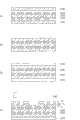
参照图1,减成工艺在绝缘层1上形成金属层2(a),将光致抗蚀剂3涂覆在金属层2上,通过曝光和显影对光致抗蚀剂层3构图(b),刻蚀金属层2以形成电路图案(c),以及移除光致抗蚀剂(d)。Referring to Fig. 1, subtractive process forms metal layer 2 (a) on
参照图2,半加成工艺在绝缘层1上形成种子层5(a),在种子层5上形成光致抗蚀剂图案3(b),将金属材料填充在光致抗蚀剂图案3中以形成电路图案3(c),移除光致抗蚀剂图案(d),以及除去种子层(e)。Referring to Fig. 2, a semi-additive process forms a seed layer 5 (a) on the
然而,由于微电路中的材料的光刻和粘合期间的图案变化,以上常规工艺难于确保微电路中的可靠性。However, it is difficult for the above conventional processes to ensure reliability in microcircuits due to pattern changes during photolithography and bonding of materials in microcircuits.
随着近来半导体芯片的高度集成以及信号传输速率的增加,需要用于实现高电气性质、高可靠性和高功能的电路小型化和PCB技术。因此,考虑如图3中所示的具有嵌入在绝缘体中的电路图案的嵌入式PCB。With recent high integration of semiconductor chips and increase in signal transmission rate, circuit miniaturization and PCB technology for realizing high electrical properties, high reliability, and high functionality are required. Therefore, consider an embedded PCB as shown in Figure 3 with a circuit pattern embedded in an insulator.
参照图3,制造嵌入式PCB的常规方法包括:步骤(a),制备具有金属层20和支撑金属层20的绝缘层10的载体基板;步骤(b),在金属层20上涂覆光致抗蚀剂并且对光致抗蚀剂构图以形成光致抗蚀剂图案30;步骤(c),利用金属材料40填充光致抗蚀剂图案30;步骤(d),移除光致抗蚀剂图案以形成电路图案;步骤(e),使绝缘层50上的载体基板与面对绝缘层50的电路图案40对准;步骤(f),使用压力朝向绝缘层50按压载体基板以将电路图案嵌入在绝缘层50中;步骤(g),移除金属层;以及步骤(h),移除绝缘层。With reference to Fig. 3, the conventional method of manufacturing embedded PCB comprises: step (a), prepares the carrier substrate that has
然而,以上的制造嵌入式PCB的常规方法是复杂的并且难于执行用于将电路图案嵌入在绝缘层中的中间层对准。因此,存在使用常规制造方法制造多层PCB的限制。However, the above conventional methods of manufacturing embedded PCBs are complicated and difficult to perform interlayer alignment for embedding circuit patterns in insulating layers. Therefore, there are limitations to fabricating multilayer PCBs using conventional fabrication methods.
发明内容Contents of the invention
本发明的目的在于提供一种制造嵌入式PCB的方法,其使用激光同时地或者顺序地刻蚀光致抗蚀剂层和绝缘层以形成电路图案以便于获得微图案并且简化制造工艺,并且实现使用嵌入式PCB的多层PCB的构造中的对准准确性,由此提高了通过该方法制造的PCB的产品可靠性和产量。The object of the present invention is to provide a method for manufacturing embedded PCB, which uses laser to etch photoresist layer and insulating layer simultaneously or sequentially to form circuit patterns so as to obtain micropatterns and simplify the manufacturing process, and realize Alignment accuracy in construction of multilayer PCBs using embedded PCBs, thereby improving product reliability and yield of PCBs manufactured by this method.
根据本发明的一个方面,一种用于制造嵌入式印刷电路板(PCB)的方法包括:第一步骤,使用激光对其上形成光致抗蚀剂层的绝缘层构图,使得有选择地刻蚀部分绝缘层以形成电路图案区域;以及第二步骤,利用镀覆材料填充电路图案区域以形成电路图案。According to one aspect of the present invention, a method for manufacturing an embedded printed circuit board (PCB) includes: a first step of patterning an insulating layer on which a photoresist layer is formed using a laser such that selectively engraved Etching part of the insulating layer to form a circuit pattern area; and a second step, filling the circuit pattern area with a plating material to form a circuit pattern.
电路图案区域可以通过如下方法形成:有选择地刻蚀掉光致抗蚀剂层的整个厚度以及有选择地刻蚀掉绝缘层的预定厚度以形成凹入图案。The circuit pattern region may be formed by selectively etching away the entire thickness of the photoresist layer and selectively etching away a predetermined thickness of the insulating layer to form a concave pattern.
电路图案区域可以通过如下方法形成:顺序地或者同时地刻蚀光致抗蚀剂层和绝缘层。The circuit pattern area may be formed by sequentially or simultaneously etching a photoresist layer and an insulating layer.
第二步骤可以包括:步骤a1,在其中形成电路图案区域的绝缘层上形成金属种子层;以及步骤a2,利用金属材料填充电路图案区域。The second step may include: a1, forming a metal seed layer on the insulating layer in which the circuit pattern area is formed; and a2, filling the circuit pattern area with a metal material.
金属种子层可以由传导聚合物或者Cu、Au、Ni、Pd、In、Ti和Sn中的一个或者至少两个形成。金属材料可以包括Cu、Ag、Sn、Au、Ni和Pd中的至少一个。The metal seed layer may be formed of a conductive polymer or one or at least two of Cu, Au, Ni, Pd, In, Ti, and Sn. The metal material may include at least one of Cu, Ag, Sn, Au, Ni, and Pd.
可以使用无电镀覆、电镀、丝网印刷、溅射、蒸发、喷墨和滴涂中的一个或者它们的组合利用金属材料对电路图案区域进行填充。The circuit pattern area may be filled with a metal material using one or a combination of electroless plating, electroplating, screen printing, sputtering, evaporation, inkjet, and drop coating.
该方法可以进一步包括第三步骤,移除电路图案上的金属种子层和光致抗蚀剂层。第三步骤可以包括如下步骤,在移除光致抗蚀剂层之前研磨电路图案的顶面。The method may further include a third step of removing the metal seed layer and the photoresist layer on the circuit pattern. The third step may include the step of grinding the top surface of the circuit pattern before removing the photoresist layer.
绝缘层可以包括载体层及其上形成的绝缘部件。The insulating layer may include a carrier layer and an insulating part formed thereon.
一种制造多层PCB的方法使包括绝缘层和在该绝缘层的顶面和/或底面上形成的电路图案的内部电路板与通过以上制造方法制造的具有部分嵌入在绝缘层中的电路图案的嵌入式PCB对准,并且层叠内部电路板和嵌入式PCB。A method of manufacturing a multilayer PCB combines an inner circuit board including an insulating layer and a circuit pattern formed on a top surface and/or a bottom surface of the insulating layer with a circuit pattern partially embedded in the insulating layer manufactured by the above manufacturing method The embedded PCB is aligned, and the internal circuit board and the embedded PCB are laminated.
电路图案是在内部电路板的顶面和底面上形成的,嵌入式PCB的电路图案可以与内部电路板的顶面和底面对准并且嵌入式PCB可以层叠在内部电路板上。The circuit pattern is formed on the top and bottom surfaces of the internal circuit board, the circuit pattern of the embedded PCB may be aligned with the top and bottom surfaces of the internal circuit board and the embedded PCB may be laminated on the internal circuit board.
根据本发明的另一方面,一种制造嵌入式PCB的方法包括:第十一步骤,在包括绝缘层和在绝缘层的顶面和/或底面上形成的电路图案的内部电路板上形成绝缘层;第十二步骤,在绝缘层上形成光致抗蚀剂层并且对光致抗蚀剂层构图,使得部分绝缘层被有选择地刻蚀以形成电路图案区域;以及第十三步骤,利用镀覆材料填充电路图案区域。According to another aspect of the present invention, a method of manufacturing an embedded PCB includes: an eleventh step of forming an insulating layer on an internal circuit board including an insulating layer and a circuit pattern formed on the top surface and/or bottom surface of the insulating layer. layer; the twelfth step, forming a photoresist layer on the insulating layer and patterning the photoresist layer, so that part of the insulating layer is selectively etched to form a circuit pattern region; and the thirteenth step, The circuit pattern area is filled with a plating material.
电路图案区域可以通过如下方法形成:有选择地刻蚀掉光致抗蚀剂层的整个厚度以及有选择地刻蚀掉绝缘层的预定厚度以形成凹入图案。电路图案区域可以通过激光加工而形成。The circuit pattern region may be formed by selectively etching away the entire thickness of the photoresist layer and selectively etching away a predetermined thickness of the insulating layer to form a concave pattern. The circuit pattern area can be formed by laser processing.
通过前文所述的根据本发明的制造方法制造的嵌入式PCB包括在绝缘层上形成的电路图案,其中部分电路图案被嵌入在绝缘层中。电路图案可以由Cu、Ag、Sn、Au、Ni和Pd中的至少一个形成。The embedded PCB manufactured by the aforementioned manufacturing method according to the present invention includes a circuit pattern formed on an insulating layer, wherein part of the circuit pattern is embedded in the insulating layer. The circuit pattern may be formed of at least one of Cu, Ag, Sn, Au, Ni, and Pd.
该嵌入式PCB可以进一步包括在除了电路图案的顶面以外的电路图案的侧面和底面上形成的金属种子层。金属种子层可以由传导聚合物或者Cu、Au、Ni、Pd、In、Ti和Sn中的一个或者至少两个形成。The embedded PCB may further include a metal seed layer formed on side and bottom surfaces of the circuit pattern except the top surface of the circuit pattern. The metal seed layer may be formed of a conductive polymer or one or at least two of Cu, Au, Ni, Pd, In, Ti, and Sn.
一种使用上文的嵌入式PCB制造的多层PCB包括:内部电路板,其包括在绝缘层的顶面和/或底面上形成的第一电路图案;以及外部电路板,其层叠在内部电路板的顶面和/或底面上,其中在外部电路板上形成的第二电路图案是在第二绝缘层上形成的,使得部分第二电路图案被嵌入在第二绝缘层中。第一和第二电路图案可以由Cu、Ag、Sn、Au、Ni和Pd中的至少一个形成。A multilayer PCB manufactured using the above embedded PCB includes: an internal circuit board including a first circuit pattern formed on a top surface and/or a bottom surface of an insulating layer; and an external circuit board laminated on the internal circuit board. On the top surface and/or the bottom surface of the board, wherein the second circuit pattern formed on the external circuit board is formed on the second insulating layer such that part of the second circuit pattern is embedded in the second insulating layer. The first and second circuit patterns may be formed of at least one of Cu, Ag, Sn, Au, Ni and Pd.
多层PCB可以进一步包括在除了第二电路图案的顶面以外的第二电路图案的侧面和底面上形成的金属种子层。金属种子层可以由传导聚合物或者Cu、Au、Ni、Pd、In、Ti和Sn中的一个或者至少两个形成。The multilayer PCB may further include a metal seed layer formed on side and bottom surfaces of the second circuit pattern except the top surface of the second circuit pattern. The metal seed layer may be formed of a conductive polymer or one or at least two of Cu, Au, Ni, Pd, In, Ti, and Sn.
根据本发明,制造嵌入式PCB的方法可以使用激光同时地或者顺序地刻蚀光致抗蚀剂层和绝缘层以形成电路图案以便于获得微图案并且简化制造工艺,并且实现使用嵌入式PCB的多层PCB的构造中的对准准确性,由此提高了产品可靠性和产量。According to the present invention, the method for manufacturing embedded PCB can use laser to simultaneously or sequentially etch photoresist layer and insulating layer to form circuit pattern so as to obtain micropattern and simplify manufacturing process, and realize the use of embedded PCB Alignment accuracy in the construction of multilayer PCBs, thereby improving product reliability and yield.
附图说明Description of drawings
所包括的附图用于提供对本发明的进一步的理解,附图被并入本申请并且构成本申请的一部分,附图图示了本发明的实施例并且与具体实施方式一起用于解释本发明的原理。在附图中:The accompanying drawings are included to provide a further understanding of the invention and are incorporated in and constitute a part of this application, illustrate embodiments of the invention and together with the detailed description serve to explain the invention principle. In the attached picture:
图1、2和3是示出制造印刷电路板(PCB)的常规方法的横截面图;1, 2 and 3 are cross-sectional views illustrating a conventional method of manufacturing a printed circuit board (PCB);
图4和5图示了根据本发明的制造嵌入式PCB的方法;4 and 5 illustrate a method of manufacturing an embedded PCB according to the present invention;
图6图示了根据本发明的实施例的制造多层PCB的工艺;以及Figure 6 illustrates a process for manufacturing a multilayer PCB according to an embodiment of the present invention; and
图7和8图示了本发明的另一实施例的制造多层PCB的工艺。7 and 8 illustrate a process of manufacturing a multi-layer PCB according to another embodiment of the present invention.
具体实施方式Detailed ways
在制造嵌入式PCB和使用嵌入式PCB的多层PCB的方法中,本发明使用激光来加工光致抗蚀剂层和绝缘层以形成电路图案以便于简化制造工艺和提高所完成的产品的可靠性。In the method of manufacturing an embedded PCB and a multilayer PCB using the embedded PCB, the present invention uses a laser to process a photoresist layer and an insulating layer to form a circuit pattern in order to simplify the manufacturing process and improve the reliability of the finished product sex.
根据本发明的制造嵌入式PCB的方法包括:第一步骤,使用激光对其上形成光致抗蚀剂层的绝缘层构图,使得有选择地刻蚀部分绝缘层以形成电路图案区域;以及第二步骤,利用镀覆材料填充电路图案区域以形成电路图案。该制造方法可以进一步包括移除光致抗蚀剂层的步骤。The method for manufacturing an embedded PCB according to the present invention includes: a first step of patterning an insulating layer on which a photoresist layer is formed using a laser, so that a part of the insulating layer is selectively etched to form a circuit pattern area; and a second step In the second step, the circuit pattern area is filled with a plating material to form a circuit pattern. The manufacturing method may further include the step of removing the photoresist layer.
现将参照其中示出本发明的示例性实施例的附图更全面地描述本发明。附图中的相同的附图标记表示相同的元件,并且因此它们的描述将被省略。尽管“第一”和“第二”用于解释各种元件,但是各个元件不受这些术语的限制并且这些术语仅用于使一个元件区别于另一元件。The present invention will now be described more fully with reference to the accompanying drawings, in which exemplary embodiments of the invention are shown. The same reference numerals in the drawings denote the same elements, and thus their descriptions will be omitted. Although 'first' and 'second' are used to explain various elements, each element is not limited by these terms and these terms are only used to distinguish one element from another.
1.制造嵌入式PCB的方法1. Method of manufacturing embedded PCB
图4和5图示了根据本发明的制造嵌入式PCB的方法。4 and 5 illustrate a method of manufacturing an embedded PCB according to the present invention.
根据本发明的制造嵌入式PCB的方法包括:第一步骤,使用激光对其上形成光致抗蚀剂层的绝缘层构图,使得有选择地刻蚀部分绝缘层以形成电路图案区域;以及第二步骤,利用镀覆材料填充电路图案区域以形成电路图案。该制造方法可以进一步包括移除光致抗蚀剂层的步骤。The method for manufacturing an embedded PCB according to the present invention includes: a first step of patterning an insulating layer on which a photoresist layer is formed using a laser, so that a part of the insulating layer is selectively etched to form a circuit pattern area; and a second step In the second step, the circuit pattern area is filled with a plating material to form a circuit pattern. The manufacturing method may further include the step of removing the photoresist layer.
具体地,在图5中示出的步骤S1和S2中,在绝缘层110和用作载体层的金属层120上形成光致抗蚀剂层130。可以使用涂覆或层叠方法来形成光致抗蚀剂层130。在步骤S3中使用激光L对光致抗蚀剂层130和部分绝缘层110进行刻蚀以形成电路图案区域。就是说,刻蚀掉光致抗蚀剂层130的整个厚度T3并且刻蚀掉绝缘层110的预定厚度T2以形成电路图案区域。随后将电路图案部分嵌入在绝缘层110的对应于厚度T2的部分中(绝缘层的总厚度=T1+T2)。可以使用激光顺序地或者同时地对光致抗蚀剂层130和绝缘层110进行刻蚀。Specifically, in steps S1 and S2 shown in FIG. 5 , a
在步骤S4中在其中定义电路图案区域的绝缘层110和光致抗蚀剂层130上形成种子层140。种子层140可以由传导聚合物或者Cu、Au、Ni、Pd、In、Ti和Sn中的一个或者至少两个形成。这里,传导聚合物可以是聚乙炔(polyacetylene)、聚吡咯(polypyrrole)、聚噻吩(polythiophene)、聚(3-烷基噻吩)(poly(3-alkylthiophene))、聚苯撑硫化物(polyphenylenesulfide)、聚苯乙炔(polyphenylenevinylene)、聚噻吩乙炔(polythienylenevinylene)、聚苯撑(polyphenylene)、聚异硫茚(polyisothianaphthene)、聚薁(polyazulene)、聚呋喃(polyfuran)和聚苯胺(polyaniline)中的至少一个。可以使用含有传导聚合物的单体的溶液和氧化聚合物溶液来形成传导聚合物层。传导聚合物的单体可以使用乙炔(acetylene)、吡咯(pyrrole)、噻吩(thiophene)、3-烷基噻吩(3-alkylthiophene)、苯撑硫化物(phenylene sulfide)、苯乙炔(phenylenevinylene)、噻吩乙炔(thienylenevinylene)、苯撑(phenylene)、异硫茚(isothianaphthene)、薁(azulene)、呋喃(furan)、苯胺(aniline)以及这些材料的衍生物中的一个。可以有选择地将有机硅烷偶联剂添加到传导聚合物的单体溶液。The
在步骤S5中将金属材料填充在其上形成种子层140的电路图案区域中以形成电路图案150。电路图案150可以由Cu、Ag、Sn、Au、Ni和Pd中的至少一个形成。可以使用无电镀覆、电镀、丝网印刷、溅射、蒸发、喷墨和滴涂中的一个或者这些方法的组合来填充形成电路图案的金属材料。A metal material is filled in the circuit pattern region on which the
在步骤S6中可以通过闪蚀或者研磨来对电路图案150的表面进行刻蚀。对电路图案150的表面和在光致抗蚀剂层130上形成的种子层进行刻蚀直至光致抗蚀剂层130的表面暴露。In step S6, the surface of the
随后,在步骤S7中移除光致抗蚀剂层130以完成嵌入式PCB。在该PCB的结构中,电路图案150部分嵌入在绝缘层110的对应于厚度T2的部分中。此外,在除了电路图案150的表面以外的电路图案150的底面和侧面上形成种子层140。这里,当电路图案150和种子层140由同一材料形成时,电路图案150和种子层140的边界可以是模糊的。随后移除载体层120。Subsequently, the
2.制造多层PCB的方法2. Method of manufacturing multi-layer PCB
现将解释根据本发明的实施例的制造使用前述嵌入式PCB的多层PCB的方法。A method of manufacturing a multilayer PCB using the aforementioned embedded PCB according to an embodiment of the present invention will now be explained.
参照图6,在步骤P1中制备通过图5中示出的步骤S1至S7制造的嵌入式PCB。可以根据绝缘层的特性来移除载体层120。Referring to FIG. 6 , an embedded PCB manufactured through steps S1 to S7 shown in FIG. 5 is prepared in step P1 . The
在步骤P2和P3中使内部电路板与嵌入式PCB对准并且将热和压力施加到对准的内部电路板和嵌入式PCB以形成多层PCB。内部电路板可以具有如下结构,其中在绝缘层160的顶面和/或底面上形成预定的电路图案170。在该情况中,可以将内部电路板和嵌入式PCB朝向彼此按压,使得嵌入式PCB的绝缘层110被插入到电路图案170以外的在内部电路板中形成的凹陷中。The inner circuit board and embedded PCB are aligned and heat and pressure are applied to the aligned inner circuit board and embedded PCB in steps P2 and P3 to form a multilayer PCB. The internal circuit board may have a structure in which a
在通过以上方法制造的多层PCB的结构中,如图6的P3中所示,电路图案170(被称为第一电路图案)被嵌入在绝缘层中并且第二电路图案150在绝缘层的表面上形成并且部分地嵌入在绝缘层中。此外,可以在除了第二电路图案150的顶面以外的第二电路图案150的侧面和底面上形成金属种子层140。这里,如果第二电路图案150和金属种子层140由同一材料形成,则第二电路图案150和金属种子层140的边界可以是模糊的。金属种子层140和第二电路图案150由与前述嵌入式PCB的材料相同的材料形成。In the structure of the multilayer PCB manufactured by the above method, as shown in P3 of FIG. Formed on the surface and partially embedded in the insulating layer. In addition, the
现将参照图7和8解释根据本发明的另一实施例的制造多层PCB的方法。A method of manufacturing a multilayer PCB according to another embodiment of the present invention will now be explained with reference to FIGS. 7 and 8 .
在本发明的当前实施例中,未使用根据本发明完成的嵌入式PCB并且通过上文的嵌入式PCB制造方法在内部电路板的顶面和底面上形成嵌入式PCB。In the current embodiment of the present invention, the embedded PCB done according to the present invention is not used and the embedded PCB is formed on the top and bottom surfaces of the inner circuit board by the above embedded PCB manufacturing method.
具体地,在步骤Q1和Q2中将绝缘层230层叠在包括绝缘层210和在绝缘层210的顶面和底面上形成的预定的第一电路图案220的内部电路板的顶面和底面上。Specifically, the insulating
在步骤Q3中在绝缘层230上形成光致抗蚀剂层240并且在步骤Q4中使用激光有选择地刻蚀光致抗蚀剂层240和绝缘层230以形成电路图案区域。这里,刻蚀掉光致抗蚀剂层240的整个厚度T3并且刻蚀掉绝缘层230的预定厚度T2。A
在步骤Q5中在电路图案区域上形成金属种子层250。金属种子层250可以由与上述种子层相同的材料形成。在步骤Q6中利用金属材料填充具有其上形成的金属种子层250的电路图案区域以形成电路图案260。该金属材料可以与上述金属材料相同。The metal seed layer 250 is formed on the circuit pattern area in step Q5. The metal seed layer 250 may be formed of the same material as the aforementioned seed layer. The circuit pattern region having the metal seed layer 250 formed thereon is filled with a metal material to form a circuit pattern 260 in step Q6. The metallic material may be the same as the aforementioned metallic materials.
当在步骤Q6中使用电镀将金属填充在电路图案区域中时,形成金属种子层250的步骤Q5是不可缺少的。然而,如果在步骤Q6中使用无电镀覆、丝网印刷、溅射、蒸发、喷墨和滴涂来填充金属材料,则可以在步骤Q5之后执行步骤Q6或者可以省略步骤Q5。The step Q5 of forming the metal seed layer 250 is indispensable when the metal is filled in the circuit pattern region using electroplating in the step Q6. However, if electroless plating, screen printing, sputtering, evaporation, inkjet, and drop coating are used to fill the metal material in step Q6, step Q6 may be performed after step Q5 or step Q5 may be omitted.
在步骤Q7中可以通过闪蚀或研磨来对电路图案260的顶面和所填充的金属材料进行刻蚀。这里,对电路图案260和光致抗蚀剂层240上形成的金属种子层250进行刻蚀直至光致抗蚀剂层240的表面暴露。随后,在步骤Q8中移除光致抗蚀剂层240以实现多层PCB。In step Q7, the top surface of the circuit pattern 260 and the filled metal material may be etched by flash etching or grinding. Here, the metal seed layer 250 formed on the circuit pattern 260 and the
根据当前实施例制造的多层PCB可以具有与根据图6中示出的上述实施例制造的多层PCB相同的结构。The multilayer PCB manufactured according to the current embodiment may have the same structure as the multilayer PCB manufactured according to the above-described embodiment shown in FIG. 6 .
尽管参照本发明的示例性实施例具体地示出和描述了本发明,但是本领域的普通技术人员将理解,在不偏离如所附权利要求限定的本发明的精神和范围的情况下,可以进行形式和细节上的各种改变。While the invention has been particularly shown and described with reference to exemplary embodiments thereof, it will be understood by those skilled in the art that, without departing from the spirit and scope of the invention as defined by the appended claims, it may be made Various changes in form and detail were made.
Claims (23)
Translated fromChineseApplications Claiming Priority (2)
| Application Number | Priority Date | Filing Date | Title |
|---|---|---|---|
| KR10-2009-0116879 | 2009-11-30 | ||
| KR1020090116879AKR101086828B1 (en) | 2009-11-30 | 2009-11-30 | Embedded printed circuit boards, multilayer printed circuit boards and methods of manufacturing the same |
Publications (2)
| Publication Number | Publication Date |
|---|---|
| CN102083280Atrue CN102083280A (en) | 2011-06-01 |
| CN102083280B CN102083280B (en) | 2014-12-17 |
Family
ID=44067984
Family Applications (1)
| Application Number | Title | Priority Date | Filing Date |
|---|---|---|---|
| CN201010588017.5AActiveCN102083280B (en) | 2009-11-30 | 2010-11-30 | Embedded printed circuit board, multi-layer printed circuit board and manufacturing method thereof |
Country Status (5)
| Country | Link |
|---|---|
| US (1) | US9265161B2 (en) |
| JP (1) | JP5291078B2 (en) |
| KR (1) | KR101086828B1 (en) |
| CN (1) | CN102083280B (en) |
| TW (1) | TWI412309B (en) |
Cited By (17)
| Publication number | Priority date | Publication date | Assignee | Title |
|---|---|---|---|---|
| CN103052268A (en)* | 2011-10-11 | 2013-04-17 | 欣兴电子股份有限公司 | How to make a circuit structure |
| CN103517570A (en)* | 2012-06-28 | 2014-01-15 | 贝尔罗斯(广州)电子部件有限公司 | Electronic circuit manufacturing method and shell body |
| CN103533764A (en)* | 2012-07-05 | 2014-01-22 | 昆山联滔电子有限公司 | Manufacturing method for forming conductor line on non-conductive substrate |
| CN103813641A (en)* | 2012-11-14 | 2014-05-21 | 昆山联滔电子有限公司 | Manufacturing method of conductor track on non-conductive carrier |
| CN104115569A (en)* | 2011-12-15 | 2014-10-22 | Lg伊诺特有限公司 | Printed circuit board and method of manufacturing the same |
| CN104255086A (en)* | 2013-02-28 | 2014-12-31 | 东海神栄电子工业株式会社 | Substrate manufacturing method, substrate, and mask film |
| CN104284514A (en)* | 2013-07-09 | 2015-01-14 | 三星电机株式会社 | Printed circuit board and method of manufacturing the same |
| CN104321928A (en)* | 2012-03-23 | 2015-01-28 | Lg伊诺特有限公司 | Antenna assembly and method of manufacturing the same |
| CN104602462A (en)* | 2013-10-30 | 2015-05-06 | 三星电机株式会社 | Printed circuit board and manufacturing method thereof |
| CN104735915A (en)* | 2013-12-20 | 2015-06-24 | 台湾立讯精密有限公司 | Method for forming conductor line on insulating substrate |
| CN104754871A (en)* | 2013-12-27 | 2015-07-01 | 深南电路有限公司 | Circuit board making method |
| US9806565B2 (en) | 2012-03-23 | 2017-10-31 | Lg Innotek Co., Ltd. | Wireless power receiver and method of manufacturing the same |
| CN110364614A (en)* | 2019-06-25 | 2019-10-22 | 东莞阿尔泰显示技术有限公司 | A kind of LED display circuit board based on sputtering process and preparation method thereof |
| CN111225498A (en)* | 2018-11-27 | 2020-06-02 | 三星电机株式会社 | Printed circuit board and method of manufacturing printed circuit board |
| CN114190002A (en)* | 2021-12-09 | 2022-03-15 | 上达电子(深圳)股份有限公司 | Forming method of semi-embedded thick copper fine circuit of flexible packaging substrate |
| CN114650663A (en)* | 2022-03-29 | 2022-06-21 | 江苏上达半导体有限公司 | Forming method of double-sided embedded type circuit |
| CN119317037A (en)* | 2023-07-11 | 2025-01-14 | 鹏鼎控股(深圳)股份有限公司 | Method for manufacturing circuit board structure |
Families Citing this family (8)
| Publication number | Priority date | Publication date | Assignee | Title |
|---|---|---|---|---|
| CN102806789A (en)* | 2011-06-03 | 2012-12-05 | 上海安费诺永亿通讯电子有限公司 | Method for forming metal pattern on surface of insulator |
| JP5521130B1 (en)* | 2012-08-30 | 2014-06-11 | パナソニック株式会社 | Electronic component package and manufacturing method thereof |
| CN104335343A (en) | 2012-09-05 | 2015-02-04 | 松下知识产权经营株式会社 | Semiconductor device and method for producing same |
| KR101762778B1 (en) | 2014-03-04 | 2017-07-28 | 엘지이노텍 주식회사 | Wireless communication and charge substrate and wireless communication and charge device |
| CN106304651B (en)* | 2016-09-23 | 2018-10-09 | 奥士康科技股份有限公司 | Automate PCB manufacturing process |
| CN107148155A (en)* | 2017-06-21 | 2017-09-08 | 合肥同佑电子科技有限公司 | A kind of preparation method of three dimensional integrated circuits plate |
| KR102820035B1 (en) | 2019-09-10 | 2025-06-13 | 엘지이노텍 주식회사 | Printed circuit board and mehod of manufacturing thereof |
| KR102539011B1 (en)* | 2020-11-17 | 2023-06-02 | 주식회사 엔피테크놀로지 | Manufacturing method of flexible printed circuit board |
Citations (6)
| Publication number | Priority date | Publication date | Assignee | Title |
|---|---|---|---|---|
| JPH07240568A (en)* | 1994-02-28 | 1995-09-12 | Mitsubishi Electric Corp | Circuit board and manufacturing method thereof |
| JP2001036200A (en)* | 1999-07-22 | 2001-02-09 | Yamaichi Electronics Co Ltd | Printed wiring board, method for manufacturing printed wiring board, and method for manufacturing small plastic molded product |
| EP1482772A2 (en)* | 2003-05-29 | 2004-12-01 | Ngk Spark Plug Co., Ltd | Wiring substrate, process for manufacturing the wiring substrate, and carrier sheet for green sheet used in the manufacturing process |
| CN101198219A (en)* | 2006-12-06 | 2008-06-11 | 日立比亚机械股份有限公司 | Method for producing printed circuit board and machine for processing the same |
| US20090000813A1 (en)* | 2007-06-29 | 2009-01-01 | Phoenix Precision Technology Corporation | Packaging substrate structure and manufacturing method thereof |
| CN101493547A (en)* | 2008-01-24 | 2009-07-29 | 日东电工株式会社 | Manufacturing method of opto-electric hybrid board and opto-electric hybrid board obtained thereby |
Family Cites Families (6)
| Publication number | Priority date | Publication date | Assignee | Title |
|---|---|---|---|---|
| TWI311035B (en) | 2005-12-29 | 2009-06-11 | Subtron Technology Co Ltd | Process and structure of printed wiring board |
| KR100857165B1 (en)* | 2007-04-13 | 2008-09-05 | 삼성전기주식회사 | Circuit Board Manufacturing Method |
| KR100905566B1 (en) | 2007-04-30 | 2009-07-02 | 삼성전기주식회사 | Carrier member for circuit transfer, coreless printed circuit board using the same, and manufacturing method thereof |
| KR100897650B1 (en) | 2007-08-31 | 2009-05-14 | 삼성전기주식회사 | Manufacturing method of multilayer printed circuit board |
| TWI365022B (en) | 2008-11-13 | 2012-05-21 | Unimicron Technology Corp | Anchored circuit structure and method for making the same |
| JP2011023428A (en)* | 2009-07-13 | 2011-02-03 | Sumitomo Bakelite Co Ltd | Method for manufacturing composite, and composite |
- 2009
- 2009-11-30KRKR1020090116879Apatent/KR101086828B1/enactiveActive
- 2010
- 2010-11-30CNCN201010588017.5Apatent/CN102083280B/enactiveActive
- 2010-11-30TWTW099141490Apatent/TWI412309B/enactive
- 2010-11-30USUS12/956,545patent/US9265161B2/enactiveActive
- 2010-11-30JPJP2010267273Apatent/JP5291078B2/enactiveActive
Patent Citations (6)
| Publication number | Priority date | Publication date | Assignee | Title |
|---|---|---|---|---|
| JPH07240568A (en)* | 1994-02-28 | 1995-09-12 | Mitsubishi Electric Corp | Circuit board and manufacturing method thereof |
| JP2001036200A (en)* | 1999-07-22 | 2001-02-09 | Yamaichi Electronics Co Ltd | Printed wiring board, method for manufacturing printed wiring board, and method for manufacturing small plastic molded product |
| EP1482772A2 (en)* | 2003-05-29 | 2004-12-01 | Ngk Spark Plug Co., Ltd | Wiring substrate, process for manufacturing the wiring substrate, and carrier sheet for green sheet used in the manufacturing process |
| CN101198219A (en)* | 2006-12-06 | 2008-06-11 | 日立比亚机械股份有限公司 | Method for producing printed circuit board and machine for processing the same |
| US20090000813A1 (en)* | 2007-06-29 | 2009-01-01 | Phoenix Precision Technology Corporation | Packaging substrate structure and manufacturing method thereof |
| CN101493547A (en)* | 2008-01-24 | 2009-07-29 | 日东电工株式会社 | Manufacturing method of opto-electric hybrid board and opto-electric hybrid board obtained thereby |
Cited By (30)
| Publication number | Priority date | Publication date | Assignee | Title |
|---|---|---|---|---|
| CN103052268A (en)* | 2011-10-11 | 2013-04-17 | 欣兴电子股份有限公司 | How to make a circuit structure |
| CN103052268B (en)* | 2011-10-11 | 2016-03-02 | 欣兴电子股份有限公司 | How to make a circuit structure |
| CN104115569A (en)* | 2011-12-15 | 2014-10-22 | Lg伊诺特有限公司 | Printed circuit board and method of manufacturing the same |
| CN104115569B (en)* | 2011-12-15 | 2018-11-13 | Lg伊诺特有限公司 | Printed circuit board and manufacturing methods |
| US9806565B2 (en) | 2012-03-23 | 2017-10-31 | Lg Innotek Co., Ltd. | Wireless power receiver and method of manufacturing the same |
| CN104321928B (en)* | 2012-03-23 | 2017-10-24 | Lg 伊诺特有限公司 | Antenna assembly and method of manufacturing the same |
| US10804740B2 (en) | 2012-03-23 | 2020-10-13 | Lg Innotek Co., Ltd. | Wireless power receiver and method of manufacturing the same |
| CN104321928A (en)* | 2012-03-23 | 2015-01-28 | Lg伊诺特有限公司 | Antenna assembly and method of manufacturing the same |
| US10673141B2 (en) | 2012-03-23 | 2020-06-02 | Lg Innotek Co., Ltd. | Antenna assembly and method for manufacturing same |
| US10277071B2 (en) | 2012-03-23 | 2019-04-30 | Lg Innotek Co., Ltd. | Wireless power receiver and method of manufacturing the same |
| US10270291B2 (en) | 2012-03-23 | 2019-04-23 | Lg Innotek Co., Ltd. | Wireless power receiver and method of manufacturing the same |
| US10256540B2 (en) | 2012-03-23 | 2019-04-09 | Lg Innotek Co., Ltd. | Antenna assembly and method for manufacturing same |
| US9553476B2 (en) | 2012-03-23 | 2017-01-24 | Lg Innotek Co., Ltd. | Antenna assembly and method for manufacturing same |
| CN103517570A (en)* | 2012-06-28 | 2014-01-15 | 贝尔罗斯(广州)电子部件有限公司 | Electronic circuit manufacturing method and shell body |
| CN103533764A (en)* | 2012-07-05 | 2014-01-22 | 昆山联滔电子有限公司 | Manufacturing method for forming conductor line on non-conductive substrate |
| CN103813641A (en)* | 2012-11-14 | 2014-05-21 | 昆山联滔电子有限公司 | Manufacturing method of conductor track on non-conductive carrier |
| US9857687B2 (en) | 2013-02-28 | 2018-01-02 | Tokai Shinei Electronics Inidustry Co., Ltd | Method of manufacturing substrate and substrate and mask film |
| CN104255086B (en)* | 2013-02-28 | 2018-09-18 | 东海神栄电子工业株式会社 | Manufacturing method, substrate and the masking film of substrate |
| CN104255086A (en)* | 2013-02-28 | 2014-12-31 | 东海神栄电子工业株式会社 | Substrate manufacturing method, substrate, and mask film |
| CN104284514A (en)* | 2013-07-09 | 2015-01-14 | 三星电机株式会社 | Printed circuit board and method of manufacturing the same |
| CN104602462A (en)* | 2013-10-30 | 2015-05-06 | 三星电机株式会社 | Printed circuit board and manufacturing method thereof |
| CN104735915A (en)* | 2013-12-20 | 2015-06-24 | 台湾立讯精密有限公司 | Method for forming conductor line on insulating substrate |
| CN104754871B (en)* | 2013-12-27 | 2019-02-05 | 深南电路有限公司 | A kind of circuit board manufacturing method |
| CN104754871A (en)* | 2013-12-27 | 2015-07-01 | 深南电路有限公司 | Circuit board making method |
| CN111225498A (en)* | 2018-11-27 | 2020-06-02 | 三星电机株式会社 | Printed circuit board and method of manufacturing printed circuit board |
| CN110364614A (en)* | 2019-06-25 | 2019-10-22 | 东莞阿尔泰显示技术有限公司 | A kind of LED display circuit board based on sputtering process and preparation method thereof |
| CN114190002A (en)* | 2021-12-09 | 2022-03-15 | 上达电子(深圳)股份有限公司 | Forming method of semi-embedded thick copper fine circuit of flexible packaging substrate |
| CN114650663A (en)* | 2022-03-29 | 2022-06-21 | 江苏上达半导体有限公司 | Forming method of double-sided embedded type circuit |
| CN114650663B (en)* | 2022-03-29 | 2024-05-17 | 江苏上达半导体有限公司 | Forming method of double-sided embedded circuit |
| CN119317037A (en)* | 2023-07-11 | 2025-01-14 | 鹏鼎控股(深圳)股份有限公司 | Method for manufacturing circuit board structure |
Also Published As
| Publication number | Publication date |
|---|---|
| TWI412309B (en) | 2013-10-11 |
| KR101086828B1 (en) | 2011-11-25 |
| US20110127070A1 (en) | 2011-06-02 |
| CN102083280B (en) | 2014-12-17 |
| KR20110060325A (en) | 2011-06-08 |
| TW201132257A (en) | 2011-09-16 |
| JP2011119733A (en) | 2011-06-16 |
| US9265161B2 (en) | 2016-02-16 |
| JP5291078B2 (en) | 2013-09-18 |
Similar Documents
| Publication | Publication Date | Title |
|---|---|---|
| CN102083280B (en) | Embedded printed circuit board, multi-layer printed circuit board and manufacturing method thereof | |
| US7867888B2 (en) | Flip-chip package substrate and a method for fabricating the same | |
| KR100782405B1 (en) | Printed Circuit Board Manufacturing Method | |
| JP4558776B2 (en) | Circuit board manufacturing method | |
| US8785789B2 (en) | Printed circuit board and method for manufacturing the same | |
| US20060016553A1 (en) | Method of fabricating high density printed circuit board | |
| JP2008060573A (en) | Manufacturing method of printed circuit board with built-in electronic elements | |
| KR100757910B1 (en) | A buried pattern board and its manufacturing method | |
| KR20040014287A (en) | Method of manufacturing circuit board and communication appliance | |
| US20120175162A1 (en) | Printed circuit board | |
| US7728234B2 (en) | Coreless thin substrate with embedded circuits in dielectric layers and method for manufacturing the same | |
| US8378225B2 (en) | Printed circuit board and method for fabricating the same | |
| CN102577642A (en) | Printed circuit board and manufacturing method thereof | |
| KR101067214B1 (en) | Printed circuit board and manufacturing method thereof | |
| TWI470757B (en) | Package substrate and fabrication method thereof | |
| US20170094786A1 (en) | Printed circuit board and method of manufacturing the same | |
| CN110366310A (en) | Rigid-flex composite board and its manufacturing method | |
| KR101110361B1 (en) | PCB and Fabricating Method of the same | |
| US20100193232A1 (en) | Printed circuit board and method of manufacturing the same | |
| CN101262741B (en) | Method for forming measuring target point for measuring substrate size in substrate process | |
| KR20110131040A (en) | Embedded printed circuit board and its manufacturing method | |
| KR100468195B1 (en) | A manufacturing process of multi-layer printed circuit board | |
| JP2009200294A (en) | Laminated substrate, and its manufacturing method | |
| KR101158494B1 (en) | PCB and Fabricating Method of the same | |
| CN100505978C (en) | circuit board |
Legal Events
| Date | Code | Title | Description |
|---|---|---|---|
| C06 | Publication | ||
| PB01 | Publication | ||
| C10 | Entry into substantive examination | ||
| SE01 | Entry into force of request for substantive examination | ||
| C14 | Grant of patent or utility model | ||
| GR01 | Patent grant |