CN102077356A - Gate Dielectric Treatment for High Performance Metal Oxide and Metal Oxide Thin Film Transistors - Google Patents
Gate Dielectric Treatment for High Performance Metal Oxide and Metal Oxide Thin Film TransistorsDownload PDFInfo
- Publication number
- CN102077356A CN102077356ACN2009801258889ACN200980125888ACN102077356ACN 102077356 ACN102077356 ACN 102077356ACN 2009801258889 ACN2009801258889 ACN 2009801258889ACN 200980125888 ACN200980125888 ACN 200980125888ACN 102077356 ACN102077356 ACN 102077356A
- Authority
- CN
- China
- Prior art keywords
- layer
- gate dielectric
- plasma
- silicon oxide
- semiconductor layer
- Prior art date
- Legal status (The legal status is an assumption and is not a legal conclusion. Google has not performed a legal analysis and makes no representation as to the accuracy of the status listed.)
- Pending
Links
Images


Classifications
- H—ELECTRICITY
- H10—SEMICONDUCTOR DEVICES; ELECTRIC SOLID-STATE DEVICES NOT OTHERWISE PROVIDED FOR
- H10D—INORGANIC ELECTRIC SEMICONDUCTOR DEVICES
- H10D30/00—Field-effect transistors [FET]
- H10D30/60—Insulated-gate field-effect transistors [IGFET]
- H10D30/67—Thin-film transistors [TFT]
- H10D30/674—Thin-film transistors [TFT] characterised by the active materials
- H10D30/6755—Oxide semiconductors, e.g. zinc oxide, copper aluminium oxide or cadmium stannate
- H—ELECTRICITY
- H01—ELECTRIC ELEMENTS
- H01L—SEMICONDUCTOR DEVICES NOT COVERED BY CLASS H10
- H01L21/00—Processes or apparatus adapted for the manufacture or treatment of semiconductor or solid state devices or of parts thereof
- H01L21/02—Manufacture or treatment of semiconductor devices or of parts thereof
- H01L21/02104—Forming layers
- H01L21/02365—Forming inorganic semiconducting materials on a substrate
- H01L21/02518—Deposited layers
- H01L21/02521—Materials
- H01L21/02551—Group 12/16 materials
- H01L21/02554—Oxides
- H—ELECTRICITY
- H01—ELECTRIC ELEMENTS
- H01L—SEMICONDUCTOR DEVICES NOT COVERED BY CLASS H10
- H01L21/00—Processes or apparatus adapted for the manufacture or treatment of semiconductor or solid state devices or of parts thereof
- H01L21/02—Manufacture or treatment of semiconductor devices or of parts thereof
- H01L21/02104—Forming layers
- H01L21/02365—Forming inorganic semiconducting materials on a substrate
- H01L21/02518—Deposited layers
- H01L21/02521—Materials
- H01L21/02565—Oxide semiconducting materials not being Group 12/16 materials, e.g. ternary compounds
- H—ELECTRICITY
- H01—ELECTRIC ELEMENTS
- H01L—SEMICONDUCTOR DEVICES NOT COVERED BY CLASS H10
- H01L21/00—Processes or apparatus adapted for the manufacture or treatment of semiconductor or solid state devices or of parts thereof
- H01L21/02—Manufacture or treatment of semiconductor devices or of parts thereof
- H01L21/02104—Forming layers
- H01L21/02365—Forming inorganic semiconducting materials on a substrate
- H01L21/02612—Formation types
- H01L21/02617—Deposition types
- H01L21/02631—Physical deposition at reduced pressure, e.g. MBE, sputtering, evaporation
- H—ELECTRICITY
- H10—SEMICONDUCTOR DEVICES; ELECTRIC SOLID-STATE DEVICES NOT OTHERWISE PROVIDED FOR
- H10D—INORGANIC ELECTRIC SEMICONDUCTOR DEVICES
- H10D30/00—Field-effect transistors [FET]
- H10D30/01—Manufacture or treatment
- H10D30/021—Manufacture or treatment of FETs having insulated gates [IGFET]
- H10D30/031—Manufacture or treatment of FETs having insulated gates [IGFET] of thin-film transistors [TFT]
- H—ELECTRICITY
- H10—SEMICONDUCTOR DEVICES; ELECTRIC SOLID-STATE DEVICES NOT OTHERWISE PROVIDED FOR
- H10D—INORGANIC ELECTRIC SEMICONDUCTOR DEVICES
- H10D30/00—Field-effect transistors [FET]
- H10D30/60—Insulated-gate field-effect transistors [IGFET]
- H10D30/67—Thin-film transistors [TFT]
- H10D30/6704—Thin-film transistors [TFT] having supplementary regions or layers in the thin films or in the insulated bulk substrates for controlling properties of the device
Landscapes
- Engineering & Computer Science (AREA)
- Microelectronics & Electronic Packaging (AREA)
- Condensed Matter Physics & Semiconductors (AREA)
- General Physics & Mathematics (AREA)
- Manufacturing & Machinery (AREA)
- Computer Hardware Design (AREA)
- Physics & Mathematics (AREA)
- Power Engineering (AREA)
- Thin Film Transistor (AREA)
- Formation Of Insulating Films (AREA)
- Electrodes Of Semiconductors (AREA)
- Physical Vapour Deposition (AREA)
- Chemical Vapour Deposition (AREA)
- Physical Deposition Of Substances That Are Components Of Semiconductor Devices (AREA)
Abstract
Description
Translated fromChinese技术领域technical field
本发明的实施例大体上是关于制造薄膜晶体管(TFT)的方法。Embodiments of the invention generally relate to methods of fabricating thin film transistors (TFTs).
背景技术Background technique
因TFT阵列可用在常用于计算机和电视平面面板的液晶主动矩阵显示器(LCD),故现时对这些装置特别感兴趣。LCD还设有发光二极管(LED)做为背光。另外,有机发光二极管(OLED)已用于主动矩阵显示器,且这些OLED需要TFT来处理显示器的动作。These devices are of particular interest at present because TFT arrays can be used in liquid crystal active matrix displays (LCDs) commonly used in flat panels for computers and televisions. The LCD also has a light emitting diode (LED) as a backlight. In addition, organic light emitting diodes (OLEDs) have been used in active matrix displays, and these OLEDs require TFTs to handle the operation of the display.
以非晶硅制作的TFT已成为平面面板显示器产业的关键组件。可惜非晶硅有其限制,例如低迁移率。OLED所需的迁移率至少是非晶硅所能达到的十倍以上。此外,OLED显示器为电流驱动组件,故易受Vth漂移影响。高电流或高偏压电压下引起非晶硅TFT的Vth漂移乃急待解决的问题。另一方面,多晶硅的迁移率比非晶硅高。多晶硅为结晶体,其会造成局部沉积不均匀。制造多晶硅膜需进行复杂的退火工艺,因此使用多晶硅来制造大面积显示器比起非晶硅更困难、也更昂贵。由于非晶硅的限制,导致OLED发展渐缓。TFTs made of amorphous silicon have become key components in the flat panel display industry. Unfortunately, amorphous silicon has its limitations, such as low mobility. The mobility required for OLEDs is at least ten times that of amorphous silicon. In addition, OLED displays are current-driven components, so they are susceptible to Vth drift. The Vth shift of amorphous silicon TFT caused by high current or high bias voltage is an urgent problem to be solved. On the other hand, polysilicon has higher mobility than amorphous silicon. Polysilicon is crystalline, which causes local uneven deposition. Manufacturing polysilicon films requires a complex annealing process, so it is more difficult and more expensive to manufacture large-area displays using polysilicon than amorphous silicon. Due to the limitation of amorphous silicon, the development of OLED has been slowed down.
近年来已开发透明TFT,其中氧化锌当作主动通道层。氧化锌为化合物半导体,其可在相当低的沉积温度下长成结晶材料至如玻璃和塑料等各种基板上。In recent years transparent TFTs have been developed in which zinc oxide acts as the active channel layer. Zinc oxide is a compound semiconductor that can be grown as a crystalline material onto various substrates such as glass and plastic at relatively low deposition temperatures.
故此技艺需要具非晶主动通道且迁移率高的TFT。Therefore, this technology requires a TFT with an amorphous active channel and high mobility.
发明内容Contents of the invention
本发明大体上包括薄膜晶体管(TFT)和其制造方法。TFT的栅极介电层会影响TFT的临界电压。经由在沉积主动通道材料前处理栅极介电层,可改进临界电压。处理栅极介电层的一方法涉及使栅极介电层接触一氧化二氮(N2O)气体。处理栅极介电层的另一方法涉及使栅极介电层接触N2O等离子体。氧化硅虽未实际应用到硅基TFT的栅极介电层,但其用于金属氧化物TFT时,也可改进临界电压。经由处理栅极介电层及/或使用氧化硅,可改进TFT的次临界斜率和临界电压。The present invention generally includes thin film transistors (TFTs) and methods of making the same. The gate dielectric layer of the TFT affects the threshold voltage of the TFT. Threshold voltage can be improved by treating the gate dielectric prior to depositing the active channel material. One method of treating the gate dielectric layer involves exposing the gate dielectric layer to nitrous oxide (N2O ) gas. Another method of treating the gate dielectric layer involves exposing the gate dielectric layer toN2O plasma. Although silicon oxide is not actually used in the gate dielectric layer of silicon-based TFTs, it can also improve the threshold voltage when used in metal oxide TFTs. By treating the gate dielectric layer and/or using silicon oxide, the subthreshold slope and threshold voltage of the TFT can be improved.
在一实施例中,揭露一种TFT制造方法。方法包括沉积栅极介电层至栅极电极和基板上、使栅极介电层接触N2O等离子体或其它等离子体而进行处理、沉积半导体层至栅极介电层上、沉积导电层至半导体层上、以及蚀刻导电层和半导体层而界定源极与漏极和主动通道。半导体层包括氧、及一或多个选自由锌、镓、铟、镉、锡和其组合构成群组的元素,或者半导体层包括氮、氧、及一或多个选自由锌、铟、锡、镓、镉和其组合构成群组的元素。主动通道为半导体层的一部分。In one embodiment, a TFT manufacturing method is disclosed. The method includes depositing a gate dielectric layer on the gate electrode and the substrate, exposing the gate dielectric layer toN2O plasma or other plasma for treatment, depositing a semiconductor layer on the gate dielectric layer, depositing a conductive layer onto the semiconductor layer, and etching the conductive layer and the semiconductor layer to define source and drain electrodes and active channels. The semiconductor layer includes oxygen, and one or more elements selected from the group consisting of zinc, gallium, indium, cadmium, tin, and combinations thereof, or the semiconductor layer includes nitrogen, oxygen, and one or more elements selected from the group consisting of zinc, indium, tin , gallium, cadmium and their combinations form the elements of the group. The active channel is part of the semiconductor layer.
在另一实施例中,揭露一种TFT制造方法。方法包括沉积氮化硅层至栅极电极和基板上、沉积氧化硅层至氮化硅层上、沉积半导体层至氧化硅层上、沉积导电层至半导体层上、以及蚀刻导电层而界定源极与漏极和主动通道。半导体层包括氧、及一或多个选自由锌、镓、铟、镉、锡和其组合构成群组的元素,或者半导体层包括氮、氧、及一或多个选自由锌、铟、锡、镓、镉和其组合构成群组的元素。主动通道为半导体层的一部分。In another embodiment, a TFT manufacturing method is disclosed. The method includes depositing a silicon nitride layer on the gate electrode and the substrate, depositing a silicon oxide layer on the silicon nitride layer, depositing a semiconductor layer on the silicon oxide layer, depositing a conductive layer on the semiconductor layer, and etching the conductive layer to define source pole and drain and active channel. The semiconductor layer includes oxygen, and one or more elements selected from the group consisting of zinc, gallium, indium, cadmium, tin, and combinations thereof, or the semiconductor layer includes nitrogen, oxygen, and one or more elements selected from the group consisting of zinc, indium, tin , gallium, cadmium and their combinations form the elements of the group. The active channel is part of the semiconductor layer.
在又一实施例中,揭露一种TFT制造方法。方法包括沉积氧化硅层至栅极电极和基板上、沉积半导体层至氧化硅层上、沉积导电层至半导体层上、以及蚀刻导电层而界定源极与漏极和主动通道。半导体层包括氧、及一或多个选自由锌、镓、铟、镉、锡和其组合构成群组的元素,或者半导体层包括氮、氧、及一或多个选自由锌、铟、锡、镓、镉和其组合构成群组的元素。主动通道暴露出部分半导体层。In yet another embodiment, a TFT manufacturing method is disclosed. The method includes depositing a silicon oxide layer on the gate electrode and the substrate, depositing a semiconductor layer on the silicon oxide layer, depositing a conductive layer on the semiconductor layer, and etching the conductive layer to define source and drain electrodes and an active channel. The semiconductor layer includes oxygen, and one or more elements selected from the group consisting of zinc, gallium, indium, cadmium, tin, and combinations thereof, or the semiconductor layer includes nitrogen, oxygen, and one or more elements selected from the group consisting of zinc, indium, tin , gallium, cadmium and their combinations form the elements of the group. The active channel exposes part of the semiconductor layer.
在再一实施例中,揭露一种TFT。TFT包括氧化硅层,位于栅极电极和基板上、半导体层,位于氧化硅层上、以及源极与漏极,位于半导体层上。半导体层包括氧、及一或多个选自由锌、镓、铟、镉、锡和其组合构成群组的元素,或者半导体层包括氮、氧、及一或多个选自由锌、铟、锡、镓、镉和其组合构成群组的元素。源极和漏极彼此相隔而暴露出部分半导体层。In yet another embodiment, a TFT is disclosed. The TFT includes a silicon oxide layer on a gate electrode and a substrate, a semiconductor layer on the silicon oxide layer, and source and drain electrodes on the semiconductor layer. The semiconductor layer includes oxygen, and one or more elements selected from the group consisting of zinc, gallium, indium, cadmium, tin, and combinations thereof, or the semiconductor layer includes nitrogen, oxygen, and one or more elements selected from the group consisting of zinc, indium, tin , gallium, cadmium and their combinations form the elements of the group. The source and the drain are separated from each other to expose part of the semiconductor layer.
附图说明Description of drawings
为让本发明的上述特征更明显易懂,可配合参考实施例说明,其部分乃绘示如附图式。须注意的是,虽然所附图式揭露本发明特定实施例,但其并非用以限定本发明的精神与范围,任何熟习此技艺者,当可作各种的更动与润饰而得等效实施例。In order to make the above-mentioned features of the present invention more comprehensible, reference may be made to the description of the embodiments, some of which are shown in the accompanying drawings. It should be noted that although the accompanying drawings disclose specific embodiments of the present invention, they are not intended to limit the spirit and scope of the present invention. Anyone skilled in the art can make various changes and modifications to obtain equivalents Example.
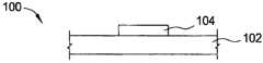
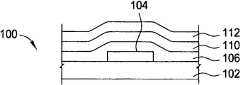
图1A-1F为根据本发明一实施例的TFT 100于不同制造阶段的截面图。1A-1F are cross-sectional views of a
图2为根据本发明另一实施例的TFT 200的截面图。FIG. 2 is a cross-sectional view of a
图3显示根据本发明一实施例,在沉积主动层材料前,等离子体处理栅极介电层的作用曲线图。FIG. 3 is a graph showing the effect of plasma treatment of the gate dielectric layer before depositing the active layer material according to an embodiment of the present invention.
图4A显示根据本发明一实施例,栅极介电层的沉积温度的作用曲线图。FIG. 4A is a graph showing the effect of deposition temperature of a gate dielectric layer according to an embodiment of the present invention.
图4B显示根据本发明一实施例,在沉积主动层材料前,以NH3等离子体处理及退火处理栅极介电层的作用曲线图。4B is a graph showing the effect of NH3 plasma treatment and annealing on the gate dielectric layer before depositing the active layer material according to an embodiment of the present invention.
图5显示根据本发明一实施例,在沉积主动层材料前,以N2O等离子体处理栅极介电层的作用曲线图。FIG. 5 is a graph showing the effect of treating the gate dielectric layer with N2 O plasma before depositing the active layer material according to an embodiment of the present invention.
图6A及6B显示根据本发明一实施例,在沉积主动层材料前,暴露于N2O中及N2O等离子体处理栅极介电层的作用曲线图。6A and 6B are graphs showing the effect of N2 O exposure and N2 O plasma treatment of the gate dielectric layer before deposition of the active layer material according to an embodiment of the present invention.
图7A及7B显示根据本发明一实施例,在沉积主动层材料前,接触N2O的温度和N2O等离子体处理栅极介电层的温度的作用曲线图。7A and 7B are graphs showing the effect of the temperature of the N2 O contact and the temperature of the N2 O plasma treatment of the gate dielectric layer before depositing the active layer material according to an embodiment of the present invention.
为助于了解,各图中共通的组件以相同的组件符号表示。应理解某一实施例所揭露的组件当可用于其它实施例,而不需特别提及。To facilitate understanding, common components in each figure are denoted by the same component symbols. It should be understood that components disclosed in one embodiment can be used in other embodiments without special mention.
具体实施方式Detailed ways
本发明大体上包括薄膜晶体管(TFT)和其制造方法。TFT的栅极介电层会影响TFT的临界电压。经由在沉积主动通道材料前处理栅极介电层,可改进临界电压。处理栅极介电层的一方法涉及在高于200℃的温度下,使栅极介电层接触一氧化二氮(N2O)气体。处理栅极介电层的另一方法涉及使栅极介电层接触N2O等离子体。氧化硅虽未实际应用到硅基TFT的栅极介电层,但其用于金属氧化物TFT时,也可改进临界电压。经由处理栅极介电层及/或使用氧化硅,可改进TFT的临界电压。氧化锌基半导体可透过掺杂制作成非晶材料。如此可避免晶粒结构引起的不均匀问题。如氧化锌基半导体的非晶半导体更易施行于目前采用底栅极TFT结构的显示器制造工艺。The present invention generally includes thin film transistors (TFTs) and methods of making the same. The gate dielectric layer of the TFT affects the threshold voltage of the TFT. Threshold voltage can be improved by treating the gate dielectric prior to depositing the active channel material. One method of treating the gate dielectric layer involves exposing the gate dielectric layer to nitrous oxide (N2O ) gas at a temperature greater than 200°C. Another method of treating the gate dielectric layer involves exposing the gate dielectric layer toN2O plasma. Although silicon oxide is not actually used in the gate dielectric layer of silicon-based TFTs, it can also improve the threshold voltage when used in metal oxide TFTs. The threshold voltage of the TFT can be improved by manipulating the gate dielectric layer and/or using silicon oxide. Zinc oxide-based semiconductors can be made into amorphous materials through doping. In this way, non-uniformity problems caused by the grain structure can be avoided. Amorphous semiconductors such as zinc oxide-based semiconductors are easier to implement in the current display manufacturing process using a bottom-gate TFT structure.
图1A-1F为根据本发明一实施例的TFT 100于不同制造阶段的截面图。TFT包含基板102。在一实施例中,基板102包含玻璃。在另一实施例中,基板102包含聚合物。在又一实施例中,基板102包含塑料。在再一实施例中,基板102包含金属。1A-1F are cross-sectional views of a
栅极电极104形成在基板上。栅极电极104包含导电层,用以控制TFT内的电荷载子移动。栅极电极104可包含金属,例如铝、钨、铬、钽或其组合。栅极电极104可以传统沉积技术形成,包括溅射、微影和蚀刻。经由毯覆沉积导电层至基板102上可形成栅极电极104。导电层可以溅射沉积而得。随后,光阻层沉积在导电层上。光阻层经图案化形成罩幕。经由蚀去导电层未遮蔽的区域并留下基板102上的栅极电极104可形成栅极电极104。The
栅极介电层106沉积于栅极电极104上。栅极介电层106会影响TFT的次临界区参数或斜率和临界电压。就硅基TFT(即具如非晶硅的硅基半导体层的TFT)而言,栅极介电层106不含氧化硅,因其将使得TFT具有相当正的Vth和低迁移率。但就金属氧化物TFT而言,已发现氧化硅可当作有效栅极介电层106。氧化硅中的氧不会大幅改变金属氧化物层或界面,故TFT不会失效。在一实施例中,栅极介电层106包含氮化硅。在另一实施例中,栅极介电层106包含氧化硅。在又一实施例中,栅极介电层106包含二氧化硅。在再一实施例中,栅极介电层106包含氮氧化硅。在另一实施例中,栅极介电层106包含氧化铝(Al2O3)。栅极介电层106可以熟知的沉积技术沉积,包括等离子体增强化学气相沉积(PECVD)。在一实施例中,栅极介电层106是以物理气相沉积(PVD)沉积而得。A
沉积栅极介电层106后,处理栅极介电层106。各种处理栅极介电层106的技术将详述于下。技术之一涉及使栅极介电层106接触等离子体108,以钝化栅极介电层106的表面。After the
处理栅极介电层106后,沉积半导体层110于其上。半导体层110将变成包含最终TFT结构的主动沟道的材料。半导体层110包含氧、及一或多个选自由锌、镓、铟、镉、锡和其组合构成群组的元素,或包含氮、氧、及一或多个选自由锌、铟、锡、镓、镉和其组合构成群组的元素。在一实施例中,半导体层110包含氧、氮、及一或多个具占满s轨域与占满d轨域的元素。在另一实施例中,半导体层110包含氧、氮、及一或多个具占满f轨域的元素。在又一实施例中,半导体层110包含氧、氮、及一或多个二价元素。在再一实施例中,半导体层110包含氧、氮、及一或多个三价元素。在另一实施例中,半导体层110包含氧、氮、及一或多个四价元素。After processing the
半导体层110还可包含掺质。适用的掺质包括铝(Al)、锡(Sn)、镓(Ga)、钙(Ca)、硅(Si)、钛(Ti)、铜(Cu)、锗(Ge)、铟(In)、镍(Ni)、锰(Mn)、铬(Cr)、钒(V)、镁(Mg)、氮化硅(SixNy)、氧化铝(AlxOy)和碳化硅(SiC)。在一实施例中,掺质包含铝。在另一实施例中,掺质包含锡。The
半导体层110的例子包括ZnOxNy、SnOxNy、InOxNy、CdOxNy、GaOxNy、ZnSnOxNy、ZnInOxNy、ZnCdOxNy、ZnGaOxNy、SnInOxNy、SnCdOxNy、SnGaOxNy、InCdOxNy、InGaOxNy、CdGaOxNy、ZnSnInOxNy、ZnSnCdOxNy、ZnSnGaOxNy、ZnInCdOxNy、ZnInGaOxNy、ZnCdGaOxNy、SnInCdOxNy、SnInGaOxNy、SnCdGaOxNy、InCdGaOxNy、ZnSnInCdOxNy、ZnSnInGaOxNy、ZnInCdGaOxNy和SnInCdGaOxNy。半导体层110的例子包括以下掺杂材料:ZnOxNy:Al、ZnOxNy:Sn、SnOxNy:Al、InOxNy:Al、InOxNy:Sn、CdOxNy:Al、CdOxNy:Sn、GaOxNy:Al、GaOxNy:Sn、ZnSnOxNy:Al、ZnInOxNy:Al、ZnInOxNy:Sn、ZnCdOxNy:Al、ZnCdOxNy:Sn、ZnGaOxNy:Al、ZnGaOxNy:Sn、SnInOxNy:Al、SnCdOxNy:Al、SnGaOxNy:Al、InCdOxNy:Al、InCdOxNy:Sn、InGaOxNy:Al、InGaOxNy:Sn、CdGaOxNy:Al、CdGaOxNy:Sn、ZnSnInOxNy:Al、ZnSnCdOxNy:Al、ZnSnGaOxNy:Al、ZnInCdOxNy:Al、ZnInCdOxNy:Sn、ZnInGaOxNy:Al、ZnInGaOxNy:Sn、ZnCdGaOxNy:Al、ZnCdGaOxNy:Sn、SnInCdOxNy:Al、SnInGaOxNy:Al、SnCdGaOxNy:Al、InCdGaOxNy:Al、InCdGaOxNy:Sn、ZnSnInCdOxNy:Al、ZnSnInGaOxNy:Al、ZnInCdGaOxNy:Al、ZnInCdGaOxNy:Sn和SnInCdGaOxNy:Al。Examplesof thesemiconductor layer 110 include ZnOxNy,SnOxNy,InOxNy,CdOxNy,GaOxNy,ZnSnOxNy,ZnInOxNy,ZnCdOxNy,ZnGaOxNy , SnInOx Ny , SnCdOx Ny , SnGaOx Ny , InCdOx Ny , InGaOx Ny , CdGaOx Ny , ZnSnInOx Ny , ZnSnCdOx Ny , ZnSnGaOx Ny , ZnInCdOx Ny , ZnInGaOx Ny , ZnCdGaOx Ny , SnInCdOx Ny , SnInGaOx Ny , SnCdGaOx Ny , InCdGaOx Ny , ZnSnInCdOx Ny , ZnSnInGaOx Ny , ZnInCdGaOx Ny , and SnInCdGaOx Ny . Examples ofthe semiconductorlayer 110 include the following doped materials:ZnOxNy: Al,ZnOxNy: Sn,SnOxNy :Al,InOxNy :Al,InOxNy: Sn,CdOxNy : Al, CdOx Ny : Sn, GaOx Ny : Al, GaOx Ny : Sn, ZnSnOx Ny : Al, ZnInOx Ny : Al, ZnInOx Ny : Sn, ZnCdOx Ny : Al, ZnCdOx Ny : Sn, ZnGaOx Ny : Al, ZnGaOx Ny : Sn, SnInOx Ny : Al, SnCdO x N y : Al, SnGaOx Ny : Al, InCdOx Ny : Al, InCdOx Ny : Al , InCdOx Ny : Sn, InGaOx Ny : Al, InGaOx Ny : Sn, CdGaOx Ny : Al, CdGaOx Ny : Sn, ZnSnInOx Ny : Al, ZnSnCdOx Ny : Al, ZnSnGaOx Ny : Al, ZnInCdOx Ny : Al, ZnInCdOx Ny : Sn, ZnInGaOx N y : Al, ZnInGaO xNy: Sn, ZnCdGaOx Ny : Al, ZnCdGaOx Ny : Sn, SnInCdOx Ny : Al, SnInGaOx Ny : Al,SnCdGaOx Ny : Al, InCdGaO x Ny : Al, InCdGaOx Ny : Sn, ZnSnInCdO x N y : Al,ZnSnInGaO xNy: Al, ZnInCdGaOxNy: Al,ZnInCdGaOxNy :Sn, andSnInCdGaOxNy :Al.
半导体层110可以溅射沉积而得。在一实施例中,溅射靶材包含金属,例如锌、镓、锡、镉、铟或其组合。溅射靶材另可包含掺质。含氧气体和含氮气体引进腔室,藉以反应溅射沉积半导体层110。在一实施例中,含氮气体包含氮气(N2)。在另一实施例中,含氮气体包含一氧化二氮(N2O)、氨气(NH3)或其组合。在一实施例中,含氧气体包含氧气(O2)。在另一实施例中,含氧气体包含N2O。含氮气体的氮和含氧气体的氧与溅射靶材的金属反应形成包含金属、氧、氮、和选择性包含掺质的半导体材料于基板上。在一实施例中,含氮气体和含氧气体为不同气体。在另一实施例中,含氮气体和含氧气体包含相同气体。溅射期间,诸如二硼烷(B2H6)、二氧化碳(CO2)、一氧化碳(CO)、甲烷(CH4)和其组合的添加剂也可额外提供给腔室。The
沉积半导体层110后,沉积导电层112。在一实施例中,导电层112包含金属,例如铝、钨、钼、铬、钽和其组合。导电层112可以溅射沉积而得。After the
沉积导电层112后,蚀去部分导电层112,以界定源极114、漏极116和主动通道118。部分半导体层110亦被蚀刻移除。尽管图未绘示,沉积导电层前,尚可沉积蚀刻终止层至半导体层110上。蚀刻终止层用来保护主动通道118,以免其于蚀刻时不当接触等离子体。After the
图2为根据本发明另一实施例的TFT 200的截面图。TFT 200包括位于基板202上的栅极电极204。其尚有源极214、漏极216、主动通道216和半导体层210。其还包括多层栅极介电层。栅极介电层具有第一栅极介电层206和第二栅极介电层208。在一实施例中,第一栅极介电层206包含氮化硅。在一实施例中,第二栅极介电层208包含氧化硅。如上所述,氧化硅虽未应用到硅基TFT,但仍有益于金属氧化物TFT。FIG. 2 is a cross-sectional view of a
实施例Example
表I列出数种TFT的比较结果,除了处理栅极介电层的方法不同外,其实质相同。各实施例的栅极介电层采用氮化硅。Table I lists the comparison results of several TFTs, which are essentially the same except for the different methods of processing the gate dielectric layer. The gate dielectric layer of each embodiment uses silicon nitride.
表ITable I


实施例1Example 1
备有氮化硅栅极介电层的TFT不加以处理。沉积栅极介电层后,半导体层沉积其上,且不让栅极介电层接触大气。TFT的迁移率为9.78平方公分/伏特-秒(cm2/V-s)、次临界斜率为2V/dec。TFTs with a silicon nitride gate dielectric were left untreated. After depositing the gate dielectric layer, a semiconductor layer is deposited thereon without exposing the gate dielectric layer to the atmosphere. The mobility of the TFT is 9.78 square centimeters per volt-second (cm2 /Vs), and the subthreshold slope is 2 V/dec.
实施例2Example 2
TFT备有氮化硅栅极介电层和氧化硅层沉积其上。栅极介电层不进一步处理。沉积氧化硅层后,半导体层沉积其上,且不让栅极介电层或氧化硅层接触大气。TFT的迁移率为7.65cm2/V-s、次临界斜率为1.48V/dec。The TFT has a silicon nitride gate dielectric layer and a silicon oxide layer deposited on it. The gate dielectric was not further processed. After depositing the silicon oxide layer, a semiconductor layer is deposited thereon without exposing the gate dielectric layer or the silicon oxide layer to the atmosphere. The mobility of the TFT was 7.65 cm2 /Vs, and the subthreshold slope was 1.48 V/dec.
实施例3Example 3
TFT备有氮化硅栅极介电层并接触N2O等离子体。半导体层沉积其上,且不让栅极介电层接触大气。TFT的迁移率为7.84cm2/V-s、次临界斜率为1.42V/dec。The TFTs are provided with a silicon nitride gate dielectric and exposed to N2 O plasma. The semiconductor layer is deposited thereon without exposing the gate dielectric layer to the atmosphere. The mobility of the TFT was 7.84 cm2 /Vs, and the subthreshold slope was 1.42 V/dec.
实施例4Example 4
TFT备有氮化硅栅极介电层并接触PH3等离子体。半导体层沉积其上,且不让栅极介电层接触大气。TFT的迁移率小于1cm2/V-s、次临界斜率大于4V/dec。The TFTs are provided with a silicon nitride gate dielectric and exposed to a PH3 plasma. The semiconductor layer is deposited thereon without exposing the gate dielectric layer to the atmosphere. The mobility of the TFT is less than 1cm2 /Vs, and the subcritical slope is greater than 4V/dec.
实施例5Example 5
TFT备有氮化硅栅极介电层并接触NH3等离子体。半导体层沉积其上,且不让栅极介电层接触大气。TFT的迁移率为6.28cm2/V-s、次临界斜率为2.34V/dec。The TFTs are provided with a silicon nitride gate dielectric and exposed toNH3 plasma. The semiconductor layer is deposited thereon without exposing the gate dielectric layer to the atmosphere. The mobility of the TFT was 6.28 cm2 /Vs, and the subthreshold slope was 2.34 V/dec.
实施例6Example 6
TFT备有氮化硅栅极介电层并接触H2等离子体。半导体层沉积其上,且不让栅极介电层接触大气。TFT的迁移率为2.5cm2/V-s、次临界斜率为2.8V/dec。The TFTs are provided with a silicon nitride gate dielectric and exposed toH2 plasma. The semiconductor layer is deposited thereon without exposing the gate dielectric layer to the atmosphere. The mobility of the TFT was 2.5 cm2 /Vs, and the subthreshold slope was 2.8 V/dec.
实施例7Example 7
TFT备有氮化硅栅极介电层并接触氩等离子体。半导体层沉积其上,且不让栅极介电层接触大气。TFT的迁移率为2.9cm2/V-s、次临界斜率为2.8V/dec。The TFT has a silicon nitride gate dielectric and is exposed to an argon plasma. The semiconductor layer is deposited thereon without exposing the gate dielectric layer to the atmosphere. The mobility of the TFT was 2.9 cm2 /Vs, and the subthreshold slope was 2.8 V/dec.
实施例8Example 8
TFT备有氮化硅栅极介电层并接触大气。半导体层接着沉积在氮化硅层上。TFT的迁移率为6.2cm2/V-s、次临界斜率为1.84V/dec。The TFT has a silicon nitride gate dielectric and is exposed to the atmosphere. A semiconductor layer is then deposited on the silicon nitride layer. The mobility of the TFT was 6.2 cm2 /Vs, and the subthreshold slope was 1.84 V/dec.
实施例9Example 9
TFT备有氮化硅栅极介电层并接触N2等离子体。半导体层沉积其上,且不让栅极介电层接触大气。TFT的迁移率为2.9cm2/V-s、次临界斜率为2.8V/dec。The TFTs are provided with a silicon nitride gate dielectric and exposed toN2 plasma. The semiconductor layer is deposited thereon without exposing the gate dielectric layer to the atmosphere. The mobility of the TFT was 2.9 cm2 /Vs, and the subthreshold slope was 2.8 V/dec.
如上述实施例所示,处理栅极介电层会影响次临界斜率和迁移率。氮化硅层附加氧化硅层将制造具有良好迁移率和极佳次临界斜率的TFT。此外,以N2O等离子体处理将制造具有良好迁移率和极佳次临界斜率的TFT。虽然氧化硅TFT和以N2O等离子体处理的迁移率均小于未经处理的TFT,但次临界斜率明显更好。反之,以氩等离子体、H2等离子体、NH3等离子体或N2等离子体处理将导致次临界斜率变得更糟。故处理栅极介电层的方式会影响TFT的效能。成信N2O等离子体中的氧会减少氮化硅或打断硅氮键及钝化表面。As shown in the above examples, manipulating the gate dielectric affects the subthreshold slope and mobility. The addition of a silicon oxide layer to a silicon nitride layer will produce a TFT with good mobility and excellent subthreshold slope. Furthermore, treatment withN2O plasma will produce TFTs with good mobility and excellent subthreshold slope. Although the mobilities of SiO TFTs and N2 O plasma treated are lower than those of untreated TFTs, the subthreshold slope is significantly better. Conversely, treatment with argon plasma,H2 plasma,NH3 plasma orN2 plasma will result in worse subcritical slope. Therefore, the method of processing the gate dielectric layer will affect the performance of the TFT. It is believed that the oxygen in theN2O plasma will reduce silicon nitride or break silicon nitrogen bonds and passivate the surface.
图3显示根据本发明一实施例,在沉积主动层材料前,等离子体处理栅极介电层的作用曲线图。图3显示四种不同结果,包括未处理、接触N2O等离子体、施予N2O等离子体后接触H2等离子体、和施予N2O等离子体后接触NH3等离子体。虽然仅以H2等离子体或NH3等离子体处理栅极介电层不会提供如上述实施例般的好结果,但施予N2O等离子体后接触H2等离子体或NH3等离子体能产生媲美只以N2O等离子体处理的次临界斜率。FIG. 3 is a graph showing the effect of plasma treatment of the gate dielectric layer before depositing the active layer material according to an embodiment of the present invention. Figure 3 shows four different results including no treatment,N2O plasma exposure,N2O plasma exposure followed byH2 plasma exposure, andN2O plasma exposure followed byNH3 plasma exposure. Although treatment of the gate dielectric withH2 plasma orNH3 plasma alone does not provide good results as in the above examples, exposure toH2 plasma orNH3 plasma after application ofN2O plasma can produce Comparable to the subcritical slope of only N2 O plasma treatment.
此亦研究额外处理栅极介电层。例如,栅极介电层接触不含等离子体的N2O气体后、接着接触N2O等离子体。This also investigates additional processing of the gate dielectric layer. For example, the gate dielectric layeris exposed to plasma-free N2O gas followed byN2O plasma.
图4A显示根据本发明一实施例,栅极介电层的沉积温度的作用曲线图。如图4A所示,相较于在350℃下沉积的氮化硅栅极介电层或在400℃下沉积且经退火处理的氧化硅栅极介电层,在200℃下沉积的氮化硅栅极介电层有更正的Vth。然氧化硅TFT的次临界斜率较小。FIG. 4A is a graph showing the effect of deposition temperature of a gate dielectric layer according to an embodiment of the present invention. As shown in Figure 4A, compared to a silicon nitride gate dielectric deposited at 350°C or an annealed silicon oxide gate dielectric deposited at 400°C, the nitride deposited at 200°C The silicon gate dielectric has a corrected Vth. However, the subthreshold slope of the silicon oxide TFT is smaller.
图4B显示根据本发明一实施例,以NH3等离子体处理栅极介电层的作用曲线图。如图4B所示,相较于在350℃下沉积且暴露于NH3中的氮化硅栅极介电层,在200℃下沉积且暴露于NH3中的氮化硅栅极介电层有更正的Vth和较小的次临界斜率。FIG. 4B is a graph showing the effect of treating the gate dielectric layer with NH3 plasma according to an embodiment of the present invention. As shown in Figure 4B, compared to the silicon nitride gate dielectric deposited at 350°C and exposed toNH3 , the silicon nitride gate dielectric layer deposited at 200°C and exposed toNH3 There is a corrected Vth and a smaller subthreshold slope.
图5显示根据本发明一实施例,在沉积主动层材料前,以N2O等离子体处理栅极介电层的作用曲线图。表II列出图5的三种TFT的迁移率和次临界斜率值。FIG. 5 is a graph showing the effect of treating the gate dielectric layer with N2 O plasma before depositing the active layer material according to an embodiment of the present invention. Table II lists the mobility and subthreshold slope values for the three TFTs of FIG. 5 .
表IITable II

在图5的TFT中,各TFT设有在200℃下沉积的氮化硅栅极介电层。TFT 2是在沉积半导体层前,以N2O等离子体处理栅极介电层而制得。相较于在沉积半导体层前未以N2O等离子体处理的TFT 1和TFT 3,TFT 2有较高的迁移率和较小的次临界斜率。未经等离子体处理的TFT差异在于TFT 3已老化4个月。In the TFTs of FIG. 5, each TFT is provided with a silicon nitride gate dielectric layer deposited at 200°
图6A及6B显示根据本发明一实施例,在沉积主动层材料前,暴露于N2O中及N2O等离子体处理栅极介电层的作用曲线图。表III列出图6A及6B的四种基板的次临界斜率和饱和迁移率。6A and 6B are graphs showing the effect of N2 O exposure and N2 O plasma treatment of the gate dielectric layer before deposition of the active layer material according to an embodiment of the present invention. Table III lists the subthreshold slopes and saturation mobilities for the four substrates of Figures 6A and 6B.
表IIITable III


N2O处理包含使沉积的栅极介电层接触N2O气体。N2O清洁包含使沉积的栅极介电层接触N2O等离子体。N2O清洁的作用比N2O处理强。但N2O处理会降低Ioff。N2O清洁和N2O处理均会降低次临界斜率。同时进行N2O清洁和N2O处理时,次临界斜率降低更甚。同时进行N2O清洁和N2O处理时,饱和迁移率亦大幅下降。如表III所示,进行N2O清洁获得的10Vds下的Vg远大于未处理或N2O处理获得的Vg。TheN2O treatment involves exposing the deposited gate dielectric layer toN2O gas. TheN2O cleaning involves exposing the deposited gate dielectric layer toN2O plasma. The effect of N2 O cleaning is stronger than that of N2 O treatment. But N2 O treatment will reduce Ioff . Both N2 O cleaning and N2 O treatment decreased the subcritical slope. When N2 O cleaning and N2 O treatment are carried out simultaneously, the subcritical slope decreases even more. When N2 O cleaning and N2 O treatment were carried out simultaneously, the saturation mobility also decreased significantly. As shown in Table III, the Vg at 10 Vds obtained with N2 O cleaning is much greater than that obtained with untreated or N2 O treated.
图7A及7B显示根据本发明一实施例,在沉积主动层材料前,接触N2O的温度和N2O等离子体处理栅极介电层的温度的作用曲线图。图7A显示在200℃下接触N2O气体及/或N2O等离子体处理的结果。图7B显示在300℃下接触N2O气体及/或N2O等离子体处理的结果。在栅极介电层接触N2O气体的情况下,先进行N2O等离子体处理。接触N2O气体对次临界斜率的影响很小。7A and 7B are graphs showing the effect of the temperature of the N2 O contact and the temperature of the N2 O plasma treatment of the gate dielectric layer before depositing the active layer material according to an embodiment of the present invention. Figure 7A shows the results of exposure toN2O gas and/orN2O plasma treatment at 200°C. Figure 7B shows the results of exposure toN2O gas and/orN2O plasma treatment at 300°C. In the case where the gate dielectric layer is exposed to N2 O gas, N2 O plasma treatment is performed first. Exposure to N2 O gas had little effect on the subcritical slope.
虽然上述已以N2O为例当作等离子体处理及气体接触的接触气体,但含氧气体也有同样的效果。例如,当理解O2、CO2和其组合可做为接触气体或等离子体气体。基板温度可维持呈室温至约400℃。在一实施例中,室温为约25℃。处理步骤可实行多个步骤,且各步骤利用不同的处理气体。例如,使用含氧气体(如N2O、O2或CO2)的初步处理可用于第一处理步骤。接着,使用不同的气体(如H2、PH3和其组合)进行第二处理步骤。在一实施例中,二步骤包含等离子体接触。在另一实施例中,第一步骤包含等离子体处理,第二步骤包含不使用等离子体的气体接触。在又一实施例中,进行超过两个以上的步骤。Although the above has taken N2 O as an example as the contact gas for plasma treatment and gas contact, oxygen-containing gas can also have the same effect. For example, it is understood thatO2 ,CO2 and combinations thereof can be used as contact gas or plasma gas. The substrate temperature can be maintained from room temperature to about 400°C. In one embodiment, the room temperature is about 25°C. The processing step can be carried out in multiple steps, and each step utilizes a different processing gas. For example, a preliminary treatment with an oxygen-containing gas such asN2O ,O2 orCO2 can be used for the first treatment step. Next, a second treatment step is performed using a different gas such as H2 , PH3 and combinations thereof. In one embodiment, the second step includes plasma contacting. In another embodiment, the first step comprises plasma treatment and the second step comprises gas contact without plasma. In yet another embodiment, more than two steps are performed.
经由将氧化硅层设于栅极介电层上、或以含氧气体处理栅极介电层,可改进TFT的次临界斜率及/或迁移率。The subthreshold slope and/or mobility of the TFT can be improved by disposing a silicon oxide layer on the gate dielectric layer or by treating the gate dielectric layer with an oxygen-containing gas.
虽然本发明已以较佳实施例揭露如上,然其并非用以限定本发明,任何熟习此技艺者,在不脱离本发明的精神和范围内,当可作各种的更动与润饰,因此本发明的保护范围当视权利要求书所界定者为准。Although the present invention has been disclosed above with preferred embodiments, it is not intended to limit the present invention. Any person skilled in the art can make various changes and modifications without departing from the spirit and scope of the present invention. Therefore The scope of protection of the present invention should be defined by the claims.
Claims (15)
Translated fromChinesePriority Applications (1)
| Application Number | Priority Date | Filing Date | Title |
|---|---|---|---|
| CN201510540494.7ACN105097951B (en) | 2008-07-02 | 2009-06-29 | Gate dielectric layer treatment for making high performance metal oxide and metal oxynitride thin film transistors |
Applications Claiming Priority (7)
| Application Number | Priority Date | Filing Date | Title |
|---|---|---|---|
| US7783108P | 2008-07-02 | 2008-07-02 | |
| US61/077,831 | 2008-07-02 | ||
| US11774708P | 2008-11-25 | 2008-11-25 | |
| US11774408P | 2008-11-25 | 2008-11-25 | |
| US61/117,747 | 2008-11-25 | ||
| US61/117,744 | 2008-11-25 | ||
| PCT/US2009/049084WO2010002803A2 (en) | 2008-07-02 | 2009-06-29 | Treatment of gate dielectric for making high performance metal oxide and metal oxynitride thin film transistors |
Related Child Applications (1)
| Application Number | Title | Priority Date | Filing Date |
|---|---|---|---|
| CN201510540494.7ADivisionCN105097951B (en) | 2008-07-02 | 2009-06-29 | Gate dielectric layer treatment for making high performance metal oxide and metal oxynitride thin film transistors |
Publications (1)
| Publication Number | Publication Date |
|---|---|
| CN102077356Atrue CN102077356A (en) | 2011-05-25 |
Family
ID=41463667
Family Applications (4)
| Application Number | Title | Priority Date | Filing Date |
|---|---|---|---|
| CN2009801255240AExpired - Fee RelatedCN102124569B (en) | 2008-07-02 | 2009-06-19 | Thin film transistors using multiple active channel layers |
| CN201510540494.7AExpired - Fee RelatedCN105097951B (en) | 2008-07-02 | 2009-06-29 | Gate dielectric layer treatment for making high performance metal oxide and metal oxynitride thin film transistors |
| CN2009801258893AExpired - Fee RelatedCN102084470B (en) | 2008-07-02 | 2009-06-29 | Capping layers for metal oxynitride TFTs |
| CN2009801258889APendingCN102077356A (en) | 2008-07-02 | 2009-06-29 | Gate Dielectric Treatment for High Performance Metal Oxide and Metal Oxide Thin Film Transistors |
Family Applications Before (3)
| Application Number | Title | Priority Date | Filing Date |
|---|---|---|---|
| CN2009801255240AExpired - Fee RelatedCN102124569B (en) | 2008-07-02 | 2009-06-19 | Thin film transistors using multiple active channel layers |
| CN201510540494.7AExpired - Fee RelatedCN105097951B (en) | 2008-07-02 | 2009-06-29 | Gate dielectric layer treatment for making high performance metal oxide and metal oxynitride thin film transistors |
| CN2009801258893AExpired - Fee RelatedCN102084470B (en) | 2008-07-02 | 2009-06-29 | Capping layers for metal oxynitride TFTs |
Country Status (6)
| Country | Link |
|---|---|
| US (6) | US8258511B2 (en) |
| JP (3) | JP5744726B2 (en) |
| KR (3) | KR101621840B1 (en) |
| CN (4) | CN102124569B (en) |
| TW (3) | TWI394282B (en) |
| WO (3) | WO2010002608A2 (en) |
Cited By (2)
| Publication number | Priority date | Publication date | Assignee | Title |
|---|---|---|---|---|
| CN103608925A (en)* | 2011-07-13 | 2014-02-26 | 应用材料公司 | Methods of manufacturing thin film transistor devices |
| CN112071749A (en)* | 2019-06-10 | 2020-12-11 | 爱思开海力士有限公司 | Semiconductor device and method of manufacturing the same |
Families Citing this family (107)
| Publication number | Priority date | Publication date | Assignee | Title |
|---|---|---|---|---|
| KR101150142B1 (en)* | 2006-04-06 | 2012-06-11 | 어플라이드 머티어리얼스, 인코포레이티드 | Reactive sputtering zinc oxide transparent conductive oxides onto large area substrates |
| EP2183780A4 (en) | 2007-08-02 | 2010-07-28 | Applied Materials Inc | THIN FILM TRANSISTORS USING THIN FILM SEMICONDUCTOR MATERIALS |
| US8980066B2 (en)* | 2008-03-14 | 2015-03-17 | Applied Materials, Inc. | Thin film metal oxynitride semiconductors |
| US8143093B2 (en)* | 2008-03-20 | 2012-03-27 | Applied Materials, Inc. | Process to make metal oxide thin film transistor array with etch stopping layer |
| US8258511B2 (en)* | 2008-07-02 | 2012-09-04 | Applied Materials, Inc. | Thin film transistors using multiple active channel layers |
| JP5345456B2 (en)* | 2008-08-14 | 2013-11-20 | 富士フイルム株式会社 | Thin film field effect transistor |
| JP5627071B2 (en) | 2008-09-01 | 2014-11-19 | 株式会社半導体エネルギー研究所 | Method for manufacturing semiconductor device |
| KR102391280B1 (en)* | 2009-03-12 | 2022-04-28 | 가부시키가이샤 한도오따이 에네루기 켄큐쇼 | Semiconductor device |
| JP5663214B2 (en)* | 2009-07-03 | 2015-02-04 | 株式会社半導体エネルギー研究所 | Method for manufacturing semiconductor device |
| CN102640294B (en)* | 2009-09-24 | 2014-12-17 | 应用材料公司 | Methods of fabricating metal oxide or metal oxynitride TFTs using wet process for source-drain metal etch |
| US8840763B2 (en)* | 2009-09-28 | 2014-09-23 | Applied Materials, Inc. | Methods for stable process in a reactive sputtering process using zinc or doped zinc target |
| KR101490726B1 (en)* | 2009-10-21 | 2015-02-09 | 가부시키가이샤 한도오따이 에네루기 켄큐쇼 | Semiconductor device |
| WO2011056710A2 (en) | 2009-11-03 | 2011-05-12 | Applied Materials, Inc. | Thin film transistors having multiple doped silicon layers |
| KR101035357B1 (en)* | 2009-12-15 | 2011-05-20 | 삼성모바일디스플레이주식회사 | An oxide semiconductor thin film transistor, a method of manufacturing the same, and an organic light emitting device having an oxide semiconductor thin film transistor |
| KR101701208B1 (en)* | 2010-01-15 | 2017-02-02 | 삼성디스플레이 주식회사 | Display substrate |
| KR102420689B1 (en) | 2010-02-26 | 2022-07-15 | 가부시키가이샤 한도오따이 에네루기 켄큐쇼 | Semiconductor device |
| KR101324760B1 (en)* | 2010-04-23 | 2013-11-05 | 가부시키가이샤 한도오따이 에네루기 켄큐쇼 | Method for manufacturing semiconductor device |
| KR20130045418A (en) | 2010-04-23 | 2013-05-03 | 가부시키가이샤 한도오따이 에네루기 켄큐쇼 | Manufacturing method of semiconductor device |
| JP5606787B2 (en)* | 2010-05-18 | 2014-10-15 | 富士フイルム株式会社 | Thin film transistor manufacturing method, thin film transistor, image sensor, X-ray sensor, and X-ray digital imaging apparatus |
| US8883555B2 (en)* | 2010-08-25 | 2014-11-11 | Semiconductor Energy Laboratory Co., Ltd. | Electronic device, manufacturing method of electronic device, and sputtering target |
| US7976727B1 (en)* | 2010-08-25 | 2011-07-12 | The United States Of America As Represented By The Secretary Of The Air Force | Chromium-doped zinc-nitro-antimony-gallium-tellurium infrared phosphors |
| TWI405335B (en)* | 2010-09-13 | 2013-08-11 | Au Optronics Corp | Semiconductor structure and method of manufacturing same |
| US8338240B2 (en)* | 2010-10-01 | 2012-12-25 | Semiconductor Energy Laboratory Co., Ltd. | Method for manufacturing transistor |
| US9911857B2 (en)* | 2010-10-29 | 2018-03-06 | Cbrite Inc. | Thin film transistor with low trap-density material abutting a metal oxide active layer and the gate dielectric |
| TWI555205B (en) | 2010-11-05 | 2016-10-21 | 半導體能源研究所股份有限公司 | Semiconductor device and method of manufacturing semiconductor device |
| TWI535014B (en) | 2010-11-11 | 2016-05-21 | 半導體能源研究所股份有限公司 | Semiconductor device and method of manufacturing same |
| TWI471946B (en) | 2010-11-17 | 2015-02-01 | Innolux Corp | Thin film transistor |
| US8912536B2 (en) | 2010-11-19 | 2014-12-16 | Samsung Electronics Co., Ltd. | Transistors, methods of manufacturing the same and electronic devices including transistors |
| CN103270601B (en)* | 2010-12-20 | 2016-02-24 | 夏普株式会社 | Semiconductor device and display unit |
| CN103283029B (en)* | 2010-12-27 | 2016-03-30 | 夏普株式会社 | Semiconductor device and manufacturing method thereof |
| KR101942701B1 (en)* | 2011-01-20 | 2019-01-29 | 가부시키가이샤 한도오따이 에네루기 켄큐쇼 | Oxide semiconductor element and semiconductor device |
| US8669552B2 (en)* | 2011-03-02 | 2014-03-11 | Applied Materials, Inc. | Offset electrode TFT structure |
| TWI624878B (en) | 2011-03-11 | 2018-05-21 | 半導體能源研究所股份有限公司 | Semiconductor device manufacturing method |
| TWI455322B (en)* | 2011-04-22 | 2014-10-01 | Au Optronics Corp | Thin film transistor and method of manufacturing same |
| US9166055B2 (en)* | 2011-06-17 | 2015-10-20 | Semiconductor Energy Laboratory Co., Ltd. | Semiconductor device and method for manufacturing the same |
| US9553195B2 (en)* | 2011-06-30 | 2017-01-24 | Applied Materials, Inc. | Method of IGZO and ZNO TFT fabrication with PECVD SiO2 passivation |
| CN103828061B (en) | 2011-10-07 | 2018-02-13 | 应用材料公司 | Carry out the method for deposit silicon-containing materials using argon-dilution |
| KR101878731B1 (en) | 2011-12-06 | 2018-07-17 | 삼성전자주식회사 | Transistor, method of manufacturing the same and electronic device including transistor |
| KR101920713B1 (en)* | 2011-12-23 | 2018-11-22 | 삼성전자주식회사 | Graphene device and method of manufacturing the same |
| TWI470808B (en) | 2011-12-28 | 2015-01-21 | Au Optronics Corp | Semiconductor component and manufacturing method thereof |
| US9120111B2 (en) | 2012-02-24 | 2015-09-01 | Rain Bird Corporation | Arc adjustable rotary sprinkler having full-circle operation and automatic matched precipitation |
| CN102593050B (en)* | 2012-03-09 | 2014-08-20 | 深超光电(深圳)有限公司 | Manufacturing method of liquid crystal display panel array substrate |
| WO2013134661A1 (en)* | 2012-03-09 | 2013-09-12 | Air Products And Chemicals, Inc. | Barrier materials for display devices |
| US8901556B2 (en) | 2012-04-06 | 2014-12-02 | Semiconductor Energy Laboratory Co., Ltd. | Insulating film, method for manufacturing semiconductor device, and semiconductor device |
| KR20130117558A (en) | 2012-04-18 | 2013-10-28 | 삼성디스플레이 주식회사 | Thin film transistor, thin film transistor array panel and manufacturing method for a thin film transistor array panel |
| KR101980195B1 (en) | 2012-05-16 | 2019-05-21 | 삼성전자주식회사 | Transistor having sulfur doped zinc oxynitride and method of manufacturing the same |
| CN103474467B (en)* | 2012-06-05 | 2016-04-13 | 元太科技工业股份有限公司 | Thin film transistor structure and array substrate thereof |
| TWI493726B (en)* | 2012-06-05 | 2015-07-21 | E Ink Holdings Inc | Thin film transistor structure and array substrate using the same |
| JP6002088B2 (en)* | 2012-06-06 | 2016-10-05 | 株式会社神戸製鋼所 | Thin film transistor |
| JP5972065B2 (en)* | 2012-06-20 | 2016-08-17 | 富士フイルム株式会社 | Thin film transistor manufacturing method |
| WO2014003086A1 (en)* | 2012-06-29 | 2014-01-03 | Semiconductor Energy Laboratory Co., Ltd. | Semiconductor device |
| KR102099445B1 (en) | 2012-06-29 | 2020-04-09 | 가부시키가이샤 한도오따이 에네루기 켄큐쇼 | Semiconductor device and method for manufacturing semiconductor device |
| KR101975929B1 (en) | 2012-06-29 | 2019-05-09 | 삼성전자주식회사 | Transistor having oxynitride channel layer and method of manufacturing the same |
| US9156043B2 (en) | 2012-07-13 | 2015-10-13 | Rain Bird Corporation | Arc adjustable rotary sprinkler with automatic matched precipitation |
| KR20140021118A (en) | 2012-08-07 | 2014-02-20 | 삼성디스플레이 주식회사 | Display device and method of manufacturing the same |
| TWI533457B (en) | 2012-09-11 | 2016-05-11 | 元太科技工業股份有限公司 | Thin film transistor |
| KR20140043526A (en) | 2012-09-21 | 2014-04-10 | 삼성디스플레이 주식회사 | Thin film transistor array and method of manufacturing the same |
| CN102891183B (en)* | 2012-10-25 | 2015-09-30 | 深圳市华星光电技术有限公司 | Thin-film transistor and active matrix flat panel display device |
| US20140117511A1 (en)* | 2012-10-30 | 2014-05-01 | Infineon Technologies Ag | Passivation Layer and Method of Making a Passivation Layer |
| TWI484559B (en)* | 2013-01-07 | 2015-05-11 | Univ Nat Chiao Tung | Semiconductor component process |
| TWI614813B (en)* | 2013-01-21 | 2018-02-11 | 半導體能源研究所股份有限公司 | Semiconductor device manufacturing method |
| JP6370048B2 (en)* | 2013-01-21 | 2018-08-08 | 株式会社半導体エネルギー研究所 | Method for manufacturing semiconductor device |
| KR102044971B1 (en) | 2013-02-12 | 2019-11-15 | 삼성디스플레이 주식회사 | Thin film transistor substrate and method of manufacturing the same |
| US20150380561A1 (en)* | 2013-03-01 | 2015-12-31 | Applied Materials, Inc. | Metal oxide tft stability improvement |
| JP2016514372A (en)* | 2013-03-12 | 2016-05-19 | アプライド マテリアルズ インコーポレイテッドApplied Materials,Incorporated | Pinhole evaluation method of dielectric film for metal oxide semiconductor TFT |
| WO2014159033A1 (en)* | 2013-03-13 | 2014-10-02 | Applied Materials, Inc. | Vth control method of multiple active layer metal oxide semiconductor tft |
| JP2016519429A (en) | 2013-03-19 | 2016-06-30 | アプライド マテリアルズ インコーポレイテッドApplied Materials,Incorporated | Multi-layer passivation or etch stop TFT |
| KR101995920B1 (en)* | 2013-04-17 | 2019-10-02 | 삼성디스플레이 주식회사 | Organic light emitting diode display |
| KR102166272B1 (en) | 2013-05-23 | 2020-10-16 | 삼성디스플레이 주식회사 | Thin film transistor, display substrate having the same and method of manufacturing a thin film transistor |
| JPWO2014196107A1 (en)* | 2013-06-04 | 2017-02-23 | 株式会社Joled | THIN FILM TRANSISTOR ELEMENT, ITS MANUFACTURING METHOD, AND DISPLAY DEVICE |
| KR20150025621A (en)* | 2013-08-29 | 2015-03-11 | 삼성전자주식회사 | Transistor, method of manufacturing the same and electronic device including transistor |
| KR102115564B1 (en) | 2013-09-24 | 2020-05-27 | 삼성디스플레이 주식회사 | Display substrate and display panel having the same |
| CN103500710B (en)* | 2013-10-11 | 2015-11-25 | 京东方科技集团股份有限公司 | A kind of thin-film transistor manufacture method, thin-film transistor and display device |
| KR102149795B1 (en)* | 2013-12-13 | 2020-08-31 | 삼성전기주식회사 | Resist film and methods of forming a pattern |
| US9246013B2 (en) | 2013-12-18 | 2016-01-26 | Intermolecular, Inc. | IGZO devices with composite channel layers and methods for forming the same |
| US20150177311A1 (en)* | 2013-12-19 | 2015-06-25 | Intermolecular, Inc. | Methods and Systems for Evaluating IGZO with Respect to NBIS |
| US9704888B2 (en) | 2014-01-08 | 2017-07-11 | Apple Inc. | Display circuitry with reduced metal routing resistance |
| US9530801B2 (en) | 2014-01-13 | 2016-12-27 | Apple Inc. | Display circuitry with improved transmittance and reduced coupling capacitance |
| KR102163730B1 (en) | 2014-03-25 | 2020-10-08 | 삼성전자주식회사 | Transistor, method of manufacturing the same and electronic device including transistor |
| CN104167448B (en)* | 2014-08-05 | 2017-06-30 | 京东方科技集团股份有限公司 | Thin film transistor (TFT) and preparation method thereof, array base palte and display device |
| CN104167449B (en)* | 2014-08-05 | 2017-09-22 | 京东方科技集团股份有限公司 | Thin film transistor (TFT) and preparation method thereof, array base palte and display device |
| KR101636146B1 (en)* | 2014-09-16 | 2016-07-07 | 한양대학교 산학협력단 | Thin film transistor, and method of fabricating the same |
| JP2016076599A (en)* | 2014-10-06 | 2016-05-12 | 株式会社Joled | Thin film transistor and method for manufacturing the same |
| JP6358595B2 (en)* | 2014-10-07 | 2018-07-18 | 株式会社Joled | Thin film transistor manufacturing method |
| KR20160065318A (en)* | 2014-11-28 | 2016-06-09 | 삼성디스플레이 주식회사 | Organic light emitting diode display |
| US9887277B2 (en)* | 2015-01-23 | 2018-02-06 | Applied Materials, Inc. | Plasma treatment on metal-oxide TFT |
| US20160240563A1 (en)* | 2015-02-13 | 2016-08-18 | Electronics And Telecommunications Research Institute | Semiconductor device and method of fabricating the same |
| CN104795449B (en)* | 2015-04-16 | 2016-04-27 | 京东方科技集团股份有限公司 | Thin-film transistor and manufacture method, array base palte, display unit |
| US20160308067A1 (en)* | 2015-04-17 | 2016-10-20 | Ishiang Shih | Metal oxynitride transistor devices |
| WO2017045135A1 (en)* | 2015-09-15 | 2017-03-23 | Boe Technology Group Co., Ltd. | Thin film transistor array substrate and fabrication method thereof, and display device |
| US9646886B1 (en) | 2015-12-30 | 2017-05-09 | International Business Machines Corporation | Tailored silicon layers for transistor multi-gate control |
| KR101707039B1 (en)* | 2016-03-21 | 2017-02-16 | 삼성디스플레이 주식회사 | Display substrate |
| JP7154136B2 (en) | 2017-02-07 | 2022-10-17 | 株式会社半導体エネルギー研究所 | Manufacturing method of semiconductor device |
| KR102556021B1 (en)* | 2017-10-13 | 2023-07-17 | 삼성디스플레이 주식회사 | Display apparatus and manufacturing the same |
| WO2019132997A1 (en)* | 2017-12-29 | 2019-07-04 | Intel Corporation | Memory device with negative resistance materials |
| KR102520541B1 (en)* | 2018-02-14 | 2023-04-10 | 엘지디스플레이 주식회사 | Apparatus and method for manufacturing of oxide film and display device comprising the oxide film |
| TWI689096B (en)* | 2018-08-24 | 2020-03-21 | 友達光電股份有限公司 | Metal oxide crystalline structure, and display panel circuit structure and thin film transistor having the same |
| CN109637923B (en)* | 2018-11-14 | 2021-06-11 | 惠科股份有限公司 | Display substrate, manufacturing method thereof and display device |
| CN110310985A (en)* | 2019-07-05 | 2019-10-08 | 山东大学 | A kind of indium aluminum zinc oxide thin film transistor based on double active layer and its preparation method |
| CN114651085A (en)* | 2020-05-11 | 2022-06-21 | 应用材料公司 | Method and sputter deposition apparatus for depositing a thin film transistor layer on a substrate |
| CN112376024B (en)* | 2020-10-26 | 2022-08-16 | 北京北方华创微电子装备有限公司 | Preparation method of oxide film |
| US20220190121A1 (en)* | 2020-12-14 | 2022-06-16 | Intel Corporation | Transistor channel materials |
| JP7697210B2 (en)* | 2021-01-21 | 2025-06-24 | 富士電機株式会社 | Silicon carbide semiconductor device and method for manufacturing silicon carbide semiconductor device |
| US12343748B2 (en) | 2021-03-16 | 2025-07-01 | Rain Bird Corporation | Multi-mode rotor sprinkler apparatus and method |
| KR102693443B1 (en)* | 2021-03-30 | 2024-08-08 | 한양대학교 산학협력단 | InON thin film and method for manufacturing same, and transistor comprising same |
| KR102654960B1 (en) | 2021-06-17 | 2024-04-05 | 대한민국 | Sterilization cultivation facility and method therefore |
| US12434252B2 (en) | 2022-04-20 | 2025-10-07 | Rain Bird Corporation | Full-circle and part-circle rotor sprinkler |
Citations (3)
| Publication number | Priority date | Publication date | Assignee | Title |
|---|---|---|---|---|
| US4695432A (en)* | 1985-04-02 | 1987-09-22 | Centre National De La Recherche Scientifique (C.N.R.S.) | Nitrides and oxynitrides which can be used as selective detectors of reducing gases in the atmosphere, and detection device containing them |
| US20070057261A1 (en)* | 2005-09-14 | 2007-03-15 | Jeong Jae K | Transparent thin film transistor (TFT) and its method of manufacture |
| US20070093013A1 (en)* | 2005-10-20 | 2007-04-26 | Chua Thai C | Method for fabricating a gate dielectric of a field effect transistor |
Family Cites Families (137)
| Publication number | Priority date | Publication date | Assignee | Title |
|---|---|---|---|---|
| US4331737A (en)* | 1978-04-01 | 1982-05-25 | Zaidan Hojin Handotai Kenkyu Shinkokai | Oxynitride film and its manufacturing method |
| EP0030798B1 (en)* | 1979-12-17 | 1983-12-28 | Hughes Aircraft Company | Low temperature process for depositing oxide layers by photochemical vapor deposition |
| US4759993A (en)* | 1985-04-25 | 1988-07-26 | Ovonic Synthetic Materials Co., Inc. | Plasma chemical vapor deposition SiO2-x coated articles and plasma assisted chemical vapor deposition method of applying the coating |
| US4769291A (en) | 1987-02-02 | 1988-09-06 | The Boc Group, Inc. | Transparent coatings by reactive sputtering |
| US4816082A (en) | 1987-08-19 | 1989-03-28 | Energy Conversion Devices, Inc. | Thin film solar cell including a spatially modulated intrinsic layer |
| FR2638527B1 (en)* | 1988-11-02 | 1991-02-01 | Centre Nat Rech Scient | GALLIUM NITRIDE AND OXYNITRIDES USEFUL AS SELECTIVE DETECTORS OF REDUCING GASES IN THE ATMOSPHERE, PROCESS FOR THEIR PREPARATION, AND DETECTION DEVICE CONTAINING THEM |
| CA2034118A1 (en) | 1990-02-09 | 1991-08-10 | Nang Tri Tran | Solid state radiation detector |
| JP2999280B2 (en) | 1991-02-22 | 2000-01-17 | キヤノン株式会社 | Photovoltaic element |
| JP3255942B2 (en)* | 1991-06-19 | 2002-02-12 | 株式会社半導体エネルギー研究所 | Method for manufacturing inverted staggered thin film transistor |
| JP2885547B2 (en)* | 1991-07-05 | 1999-04-26 | 新日本製鐵株式会社 | Method for producing silicon dioxide thin film |
| JP2994812B2 (en) | 1991-09-26 | 1999-12-27 | キヤノン株式会社 | Solar cell |
| US5346601A (en) | 1993-05-11 | 1994-09-13 | Andrew Barada | Sputter coating collimator with integral reactive gas distribution |
| TW273067B (en) | 1993-10-04 | 1996-03-21 | Tokyo Electron Co Ltd | |
| JPH07131030A (en)* | 1993-11-05 | 1995-05-19 | Sony Corp | Display thin film semiconductor device and manufacturing method thereof |
| JP3571785B2 (en) | 1993-12-28 | 2004-09-29 | キヤノン株式会社 | Method and apparatus for forming deposited film |
| US5620523A (en) | 1994-04-11 | 1997-04-15 | Canon Sales Co., Inc. | Apparatus for forming film |
| US5522934A (en) | 1994-04-26 | 1996-06-04 | Tokyo Electron Limited | Plasma processing apparatus using vertical gas inlets one on top of another |
| US5668663A (en) | 1994-05-05 | 1997-09-16 | Donnelly Corporation | Electrochromic mirrors and devices |
| US5700699A (en) | 1995-03-16 | 1997-12-23 | Lg Electronics Inc. | Method for fabricating a polycrystal silicon thin film transistor |
| JP3306258B2 (en) | 1995-03-27 | 2002-07-24 | 三洋電機株式会社 | Method for manufacturing semiconductor device |
| JP3169337B2 (en) | 1995-05-30 | 2001-05-21 | キヤノン株式会社 | Photovoltaic element and method for manufacturing the same |
| US6969635B2 (en) | 2000-12-07 | 2005-11-29 | Reflectivity, Inc. | Methods for depositing, releasing and packaging micro-electromechanical devices on wafer substrates |
| US5716480A (en) | 1995-07-13 | 1998-02-10 | Canon Kabushiki Kaisha | Photovoltaic device and method of manufacturing the same |
| JP3625598B2 (en)* | 1995-12-30 | 2005-03-02 | 三星電子株式会社 | Manufacturing method of liquid crystal display device |
| US5625199A (en)* | 1996-01-16 | 1997-04-29 | Lucent Technologies Inc. | Article comprising complementary circuit with inorganic n-channel and organic p-channel thin film transistors |
| US6153013A (en) | 1996-02-16 | 2000-11-28 | Canon Kabushiki Kaisha | Deposited-film-forming apparatus |
| US6746959B2 (en)* | 1996-07-26 | 2004-06-08 | Lg Philips Lcd Co., Ltd. | Liquid crystal display and method |
| AU729609B2 (en) | 1996-08-28 | 2001-02-08 | Canon Kabushiki Kaisha | Photovoltaic device |
| US6159763A (en) | 1996-09-12 | 2000-12-12 | Canon Kabushiki Kaisha | Method and device for forming semiconductor thin film, and method and device for forming photovoltaic element |
| TW329558B (en)* | 1996-09-20 | 1998-04-11 | Taiwan Semiconductor Mfg Co Ltd | The method & apparatus for manufacturing DRAM & SRAM on single semiconductor chip |
| US5993594A (en) | 1996-09-30 | 1999-11-30 | Lam Research Corporation | Particle controlling method and apparatus for a plasma processing chamber |
| US6432203B1 (en) | 1997-03-17 | 2002-08-13 | Applied Komatsu Technology, Inc. | Heated and cooled vacuum chamber shield |
| US6238527B1 (en) | 1997-10-08 | 2001-05-29 | Canon Kabushiki Kaisha | Thin film forming apparatus and method of forming thin film of compound by using the same |
| JP4208281B2 (en) | 1998-02-26 | 2009-01-14 | キヤノン株式会社 | Multilayer photovoltaic device |
| TW410478B (en) | 1998-05-29 | 2000-11-01 | Lucent Technologies Inc | Thin-film transistor monolithically integrated with an organic light-emitting diode |
| DE69936526T3 (en) | 1998-06-01 | 2009-06-25 | Kaneka Corp. | SILICON THIN LAYER PHOTOELECTRIC DEVICE |
| US6488824B1 (en) | 1998-11-06 | 2002-12-03 | Raycom Technologies, Inc. | Sputtering apparatus and process for high rate coatings |
| US7235810B1 (en) | 1998-12-03 | 2007-06-26 | Semiconductor Energy Laboratory Co., Ltd. | Semiconductor device and method of fabricating the same |
| US20020084455A1 (en) | 1999-03-30 | 2002-07-04 | Jeffery T. Cheung | Transparent and conductive zinc oxide film with low growth temperature |
| US6426245B1 (en)* | 1999-07-09 | 2002-07-30 | Semiconductor Energy Laboratory Co., Ltd. | Method for manufacturing a semiconductor device |
| KR100590925B1 (en) | 1999-07-30 | 2006-06-19 | 비오이 하이디스 테크놀로지 주식회사 | Method of manufacturing thin film transistor-liquid crystal display device |
| US6228236B1 (en) | 1999-10-22 | 2001-05-08 | Applied Materials, Inc. | Sputter magnetron having two rotation diameters |
| JP4562835B2 (en) | 1999-11-05 | 2010-10-13 | 株式会社半導体エネルギー研究所 | Method for manufacturing semiconductor device |
| US6953947B2 (en) | 1999-12-31 | 2005-10-11 | Lg Chem, Ltd. | Organic thin film transistor |
| US6620719B1 (en) | 2000-03-31 | 2003-09-16 | International Business Machines Corporation | Method of forming ohmic contacts using a self doping layer for thin-film transistors |
| KR100679917B1 (en) | 2000-09-09 | 2007-02-07 | 엘지.필립스 엘시디 주식회사 | Thin Film Transistor and Manufacturing Method Thereof |
| US6787010B2 (en) | 2000-11-30 | 2004-09-07 | North Carolina State University | Non-thermionic sputter material transport device, methods of use, and materials produced thereby |
| JP2002252353A (en)* | 2001-02-26 | 2002-09-06 | Hitachi Ltd | Thin film transistor and active matrix type liquid crystal display device |
| KR100491141B1 (en) | 2001-03-02 | 2005-05-24 | 삼성에스디아이 주식회사 | TFT and Method for Fabricating the Same and Active Matrix display device and Method for fabricating the Same using the TFT |
| WO2002073313A1 (en) | 2001-03-13 | 2002-09-19 | University Of Utah | Structured organic materials and devices using low-energy particle beams |
| US6740938B2 (en)* | 2001-04-16 | 2004-05-25 | Semiconductor Energy Laboratory Co., Ltd. | Transistor provided with first and second gate electrodes with channel region therebetween |
| JP4560245B2 (en) | 2001-06-29 | 2010-10-13 | キヤノン株式会社 | Photovoltaic element |
| US20030049464A1 (en) | 2001-09-04 | 2003-03-13 | Afg Industries, Inc. | Double silver low-emissivity and solar control coatings |
| JP4090716B2 (en)* | 2001-09-10 | 2008-05-28 | 雅司 川崎 | Thin film transistor and matrix display device |
| US20030207093A1 (en) | 2001-12-03 | 2003-11-06 | Toshio Tsuji | Transparent conductive layer forming method, transparent conductive layer formed by the method, and material comprising the layer |
| CN1445821A (en) | 2002-03-15 | 2003-10-01 | 三洋电机株式会社 | Forming method of ZnO film and ZnO semiconductor layer, semiconductor element and manufacturing method thereof |
| JP3819793B2 (en)* | 2002-03-15 | 2006-09-13 | 三洋電機株式会社 | Film-forming method and semiconductor device manufacturing method |
| US6825134B2 (en) | 2002-03-26 | 2004-11-30 | Applied Materials, Inc. | Deposition of film layers by alternately pulsing a precursor and high frequency power in a continuous gas flow |
| KR100847487B1 (en)* | 2002-04-09 | 2008-07-22 | 가부시키가이샤 가네카 | Manufacturing Method of Tandem Thin Film Photoelectric Conversion Device |
| US7189992B2 (en)* | 2002-05-21 | 2007-03-13 | State Of Oregon Acting By And Through The Oregon State Board Of Higher Education On Behalf Of Oregon State University | Transistor structures having a transparent channel |
| US7339187B2 (en)* | 2002-05-21 | 2008-03-04 | State Of Oregon Acting By And Through The Oregon State Board Of Higher Education On Behalf Of Oregon State University | Transistor structures |
| SG130013A1 (en) | 2002-07-25 | 2007-03-20 | Semiconductor Energy Lab | Method of fabricating light emitting device |
| TW571342B (en)* | 2002-12-18 | 2004-01-11 | Au Optronics Corp | Method of forming a thin film transistor |
| DE60334407D1 (en) | 2002-12-31 | 2010-11-11 | Cardinal Cg Co | COATING DEVICE WITH A CLEANING DEVICE FOR SUBSTRATE AND COATING PROCESS USING SUCH A COATING DEVICE |
| JP4417072B2 (en)* | 2003-03-28 | 2010-02-17 | シャープ株式会社 | Substrate for liquid crystal display device and liquid crystal display device using the same |
| TWI227565B (en)* | 2003-04-16 | 2005-02-01 | Au Optronics Corp | Low temperature poly-Si thin film transistor and method of manufacturing the same |
| JP2004363560A (en)* | 2003-05-09 | 2004-12-24 | Seiko Epson Corp | Substrate, device, device manufacturing method, active matrix substrate manufacturing method, electro-optical device, and electronic apparatus |
| WO2004102677A1 (en) | 2003-05-13 | 2004-11-25 | Asahi Glass Company, Limited | Transparent conductive substrate for solar battery and method for producing same |
| TWI222753B (en)* | 2003-05-20 | 2004-10-21 | Au Optronics Corp | Method for forming a thin film transistor of an organic light emitting display |
| JP4344270B2 (en)* | 2003-05-30 | 2009-10-14 | セイコーエプソン株式会社 | Manufacturing method of liquid crystal display device |
| US8319219B2 (en)* | 2003-07-14 | 2012-11-27 | Semiconductor Energy Laboratory Co., Ltd. | Light-emitting device |
| US20050017244A1 (en)* | 2003-07-25 | 2005-01-27 | Randy Hoffman | Semiconductor device |
| US7816863B2 (en) | 2003-09-12 | 2010-10-19 | Semiconductor Energy Laboratory Co., Ltd. | Light emitting device and method for manufacturing the same |
| US7520790B2 (en) | 2003-09-19 | 2009-04-21 | Semiconductor Energy Laboratory Co., Ltd. | Display device and manufacturing method of display device |
| JP4823478B2 (en) | 2003-09-19 | 2011-11-24 | 株式会社半導体エネルギー研究所 | Method for manufacturing light emitting device |
| TWI224868B (en)* | 2003-10-07 | 2004-12-01 | Ind Tech Res Inst | Method of forming poly-silicon thin film transistor |
| US7026713B2 (en)* | 2003-12-17 | 2006-04-11 | Hewlett-Packard Development Company, L.P. | Transistor device having a delafossite material |
| CN1998087B (en) | 2004-03-12 | 2014-12-31 | 独立行政法人科学技术振兴机构 | Amorphous oxide and thin film transistor |
| US7145174B2 (en)* | 2004-03-12 | 2006-12-05 | Hewlett-Packard Development Company, Lp. | Semiconductor device |
| US7297977B2 (en)* | 2004-03-12 | 2007-11-20 | Hewlett-Packard Development Company, L.P. | Semiconductor device |
| US7122398B1 (en) | 2004-03-25 | 2006-10-17 | Nanosolar, Inc. | Manufacturing of optoelectronic devices |
| US8083853B2 (en) | 2004-05-12 | 2011-12-27 | Applied Materials, Inc. | Plasma uniformity control by gas diffuser hole design |
| US7125758B2 (en) | 2004-04-20 | 2006-10-24 | Applied Materials, Inc. | Controlling the properties and uniformity of a silicon nitride film by controlling the film forming precursors |
| US20050233092A1 (en) | 2004-04-20 | 2005-10-20 | Applied Materials, Inc. | Method of controlling the uniformity of PECVD-deposited thin films |
| CN103646848B (en) | 2004-06-04 | 2018-06-05 | 伊利诺伊大学评议会 | The method of assembling printable semiconductor elements and manufacture electronic device |
| US7158208B2 (en) | 2004-06-30 | 2007-01-02 | Asml Netherlands B.V. | Lithographic apparatus and device manufacturing method |
| US20060011139A1 (en) | 2004-07-16 | 2006-01-19 | Applied Materials, Inc. | Heated substrate support for chemical vapor deposition |
| KR100721555B1 (en)* | 2004-08-13 | 2007-05-23 | 삼성에스디아이 주식회사 | Thin film transistor and its manufacturing method |
| US7378286B2 (en)* | 2004-08-20 | 2008-05-27 | Sharp Laboratories Of America, Inc. | Semiconductive metal oxide thin film ferroelectric memory transistor |
| US7622338B2 (en) | 2004-08-31 | 2009-11-24 | Semiconductor Energy Laboratory Co., Ltd. | Method for manufacturing semiconductor device |
| JP2006100760A (en) | 2004-09-02 | 2006-04-13 | Casio Comput Co Ltd | Thin film transistor and manufacturing method thereof |
| CN1293606C (en) | 2004-09-30 | 2007-01-03 | 浙江大学 | Method or growing N-Al co-blended p type ZnO transistor film by two step method |
| US7382421B2 (en)* | 2004-10-12 | 2008-06-03 | Hewlett-Packard Development Company, L.P. | Thin film transistor with a passivation layer |
| EP2453481B1 (en)* | 2004-11-10 | 2017-01-11 | Canon Kabushiki Kaisha | Field effect transistor with amorphous oxide |
| JP5138163B2 (en)* | 2004-11-10 | 2013-02-06 | キヤノン株式会社 | Field effect transistor |
| TWI251349B (en)* | 2004-11-22 | 2006-03-11 | Au Optronics Corp | Method of forming thin film transistor |
| US7309895B2 (en)* | 2005-01-25 | 2007-12-18 | Hewlett-Packard Development Company, L.P. | Semiconductor device |
| US7381586B2 (en)* | 2005-06-16 | 2008-06-03 | Industrial Technology Research Institute | Methods for manufacturing thin film transistors that include selectively forming an active channel layer from a solution |
| US7691666B2 (en)* | 2005-06-16 | 2010-04-06 | Eastman Kodak Company | Methods of making thin film transistors comprising zinc-oxide-based semiconductor materials and transistors made thereby |
| US7628896B2 (en) | 2005-07-05 | 2009-12-08 | Guardian Industries Corp. | Coated article with transparent conductive oxide film doped to adjust Fermi level, and method of making same |
| KR101167661B1 (en)* | 2005-07-15 | 2012-07-23 | 삼성전자주식회사 | Wire and method for fabricating interconnection line and thin film transistor substrate and method for fabricating the same |
| US7829471B2 (en)* | 2005-07-29 | 2010-11-09 | Applied Materials, Inc. | Cluster tool and method for process integration in manufacturing of a photomask |
| US20070030569A1 (en) | 2005-08-04 | 2007-02-08 | Guardian Industries Corp. | Broad band antireflection coating and method of making same |
| KR101188425B1 (en)* | 2005-08-24 | 2012-10-05 | 엘지디스플레이 주식회사 | Etching tape and method for fabricating array substrate of liquid crystal display using the etching tape |
| JP4968660B2 (en)* | 2005-08-24 | 2012-07-04 | スタンレー電気株式会社 | Manufacturing method of ZnO-based compound semiconductor crystal and ZnO-based compound semiconductor substrate |
| JP4870404B2 (en)* | 2005-09-02 | 2012-02-08 | 財団法人高知県産業振興センター | Thin film transistor manufacturing method |
| JP2007073704A (en)* | 2005-09-06 | 2007-03-22 | Canon Inc | Semiconductor thin film |
| US20070068571A1 (en) | 2005-09-29 | 2007-03-29 | Terra Solar Global | Shunt Passivation Method for Amorphous Silicon Thin Film Photovoltaic Modules |
| EP1770788A3 (en)* | 2005-09-29 | 2011-09-21 | Semiconductor Energy Laboratory Co., Ltd. | Semiconductor device having oxide semiconductor layer and manufacturing method thereof |
| JP5064747B2 (en)* | 2005-09-29 | 2012-10-31 | 株式会社半導体エネルギー研究所 | Semiconductor device, electrophoretic display device, display module, electronic device, and method for manufacturing semiconductor device |
| JP5099740B2 (en)* | 2005-12-19 | 2012-12-19 | 財団法人高知県産業振興センター | Thin film transistor |
| US7576394B2 (en)* | 2006-02-02 | 2009-08-18 | Kochi Industrial Promotion Center | Thin film transistor including low resistance conductive thin films and manufacturing method thereof |
| KR100785038B1 (en)* | 2006-04-17 | 2007-12-12 | 삼성전자주식회사 | Amorphous ZnO based Thin Film Transistor |
| JP2007294709A (en)* | 2006-04-26 | 2007-11-08 | Epson Imaging Devices Corp | Electro-optical device, electronic apparatus, and method of manufacturing electro-optical device |
| JP4946156B2 (en)* | 2006-05-01 | 2012-06-06 | 富士ゼロックス株式会社 | SEMICONDUCTOR FILM, METHOD FOR MANUFACTURING THE SAME, LIGHT RECEIVING DEVICE USING THE SEMICONDUCTOR FILM, ELECTROPHOTOGRAPHIC PHOTOSENSITIVE BODY, PROCESS CARTRIDGE |
| US20090023959A1 (en)* | 2006-06-16 | 2009-01-22 | D Amore Michael B | Process for making dibutyl ethers from dry 1-butanol |
| JP4609797B2 (en)* | 2006-08-09 | 2011-01-12 | Nec液晶テクノロジー株式会社 | Thin film device and manufacturing method thereof |
| JP5128792B2 (en)* | 2006-08-31 | 2013-01-23 | 財団法人高知県産業振興センター | Thin film transistor manufacturing method |
| KR101340514B1 (en)* | 2007-01-24 | 2013-12-12 | 삼성디스플레이 주식회사 | Thin film transistor substrate and method of fabricating the same |
| KR100851215B1 (en)* | 2007-03-14 | 2008-08-07 | 삼성에스디아이 주식회사 | Thin film transistor and organic light emitting display device using same |
| US20080233718A1 (en)* | 2007-03-21 | 2008-09-25 | Jia-Xing Lin | Method of Semiconductor Thin Film Crystallization and Semiconductor Device Fabrication |
| CN101663762B (en)* | 2007-04-25 | 2011-09-21 | 佳能株式会社 | Oxynitride semiconductor |
| KR100982395B1 (en)* | 2007-04-25 | 2010-09-14 | 주식회사 엘지화학 | Thin film transistor and method for manufacturing same |
| US7927713B2 (en)* | 2007-04-27 | 2011-04-19 | Applied Materials, Inc. | Thin film semiconductor material produced through reactive sputtering of zinc target using nitrogen gases |
| JP5215589B2 (en)* | 2007-05-11 | 2013-06-19 | キヤノン株式会社 | Insulated gate transistor and display device |
| US20080308411A1 (en)* | 2007-05-25 | 2008-12-18 | Energy Photovoltaics, Inc. | Method and process for deposition of textured zinc oxide thin films |
| JP5241143B2 (en)* | 2007-05-30 | 2013-07-17 | キヤノン株式会社 | Field effect transistor |
| US8372250B2 (en)* | 2007-07-23 | 2013-02-12 | National Science And Technology Development Agency | Gas-timing method for depositing oxynitride films by reactive R.F. magnetron sputtering |
| EP2183780A4 (en)* | 2007-08-02 | 2010-07-28 | Applied Materials Inc | THIN FILM TRANSISTORS USING THIN FILM SEMICONDUCTOR MATERIALS |
| US20090212287A1 (en)* | 2007-10-30 | 2009-08-27 | Ignis Innovation Inc. | Thin film transistor and method for forming the same |
| US8980066B2 (en)* | 2008-03-14 | 2015-03-17 | Applied Materials, Inc. | Thin film metal oxynitride semiconductors |
| US8143093B2 (en)* | 2008-03-20 | 2012-03-27 | Applied Materials, Inc. | Process to make metal oxide thin film transistor array with etch stopping layer |
| US7879698B2 (en)* | 2008-03-24 | 2011-02-01 | Applied Materials, Inc. | Integrated process system and process sequence for production of thin film transistor arrays using doped or compounded metal oxide semiconductor |
| US8258511B2 (en)* | 2008-07-02 | 2012-09-04 | Applied Materials, Inc. | Thin film transistors using multiple active channel layers |
| EP2184783B1 (en) | 2008-11-07 | 2012-10-03 | Semiconductor Energy Laboratory Co, Ltd. | Semiconductor device and method for manufacturing the same |
| US8436350B2 (en)* | 2009-01-30 | 2013-05-07 | Semiconductor Energy Laboratory Co., Ltd. | Semiconductor device using an oxide semiconductor with a plurality of metal clusters |
| TWI489628B (en)* | 2009-04-02 | 2015-06-21 | Semiconductor Energy Lab | Semiconductor device and method of manufacturing same |
- 2009
- 2009-03-25USUS12/411,195patent/US8258511B2/ennot_activeExpired - Fee Related
- 2009-06-19CNCN2009801255240Apatent/CN102124569B/ennot_activeExpired - Fee Related
- 2009-06-19KRKR1020117002854Apatent/KR101621840B1/ennot_activeExpired - Fee Related
- 2009-06-19WOPCT/US2009/047966patent/WO2010002608A2/enactiveApplication Filing
- 2009-06-19JPJP2011516475Apatent/JP5744726B2/ennot_activeExpired - Fee Related
- 2009-06-24TWTW098121225Apatent/TWI394282B/ennot_activeIP Right Cessation
- 2009-06-29CNCN201510540494.7Apatent/CN105097951B/ennot_activeExpired - Fee Related
- 2009-06-29KRKR1020117002859Apatent/KR101774520B1/ennot_activeExpired - Fee Related
- 2009-06-29WOPCT/US2009/049084patent/WO2010002803A2/enactiveApplication Filing
- 2009-06-29KRKR1020117002862Apatent/KR101670425B1/ennot_activeExpired - Fee Related
- 2009-06-29WOPCT/US2009/049092patent/WO2010002807A2/enactiveApplication Filing
- 2009-06-29USUS12/493,718patent/US8012794B2/enactiveActive
- 2009-06-29JPJP2011516778Apatent/JP5677712B2/ennot_activeExpired - Fee Related
- 2009-06-29CNCN2009801258893Apatent/CN102084470B/ennot_activeExpired - Fee Related
- 2009-06-29JPJP2011516775Apatent/JP5677711B2/ennot_activeExpired - Fee Related
- 2009-06-29USUS12/493,699patent/US8101949B2/ennot_activeExpired - Fee Related
- 2009-06-29CNCN2009801258889Apatent/CN102077356A/enactivePending
- 2009-07-01TWTW098122272Apatent/TWI459474B/ennot_activeIP Right Cessation
- 2009-07-02TWTW098122449Apatent/TWI385729B/ennot_activeIP Right Cessation
- 2011
- 2011-08-22USUS13/215,013patent/US8809132B2/enactiveActive
- 2012
- 2012-01-20USUS13/355,316patent/US8435843B2/enactiveActive
- 2012-07-24USUS13/556,380patent/US8349669B2/enactiveActive
Patent Citations (3)
| Publication number | Priority date | Publication date | Assignee | Title |
|---|---|---|---|---|
| US4695432A (en)* | 1985-04-02 | 1987-09-22 | Centre National De La Recherche Scientifique (C.N.R.S.) | Nitrides and oxynitrides which can be used as selective detectors of reducing gases in the atmosphere, and detection device containing them |
| US20070057261A1 (en)* | 2005-09-14 | 2007-03-15 | Jeong Jae K | Transparent thin film transistor (TFT) and its method of manufacture |
| US20070093013A1 (en)* | 2005-10-20 | 2007-04-26 | Chua Thai C | Method for fabricating a gate dielectric of a field effect transistor |
Cited By (5)
| Publication number | Priority date | Publication date | Assignee | Title |
|---|---|---|---|---|
| CN103608925A (en)* | 2011-07-13 | 2014-02-26 | 应用材料公司 | Methods of manufacturing thin film transistor devices |
| CN103608925B (en)* | 2011-07-13 | 2017-06-13 | 应用材料公司 | Method for fabricating thin film transistor devices |
| CN112071749A (en)* | 2019-06-10 | 2020-12-11 | 爱思开海力士有限公司 | Semiconductor device and method of manufacturing the same |
| CN112071749B (en)* | 2019-06-10 | 2024-03-08 | 爱思开海力士有限公司 | Semiconductor device and method of manufacturing the same |
| US11935926B2 (en) | 2019-06-10 | 2024-03-19 | SK Hynix Inc. | Semiconductor device and method for fabricating the same |
Also Published As
Similar Documents
| Publication | Publication Date | Title |
|---|---|---|
| CN105097951B (en) | Gate dielectric layer treatment for making high performance metal oxide and metal oxynitride thin film transistors | |
| KR101413655B1 (en) | Method for manufacturing oxide semiconductor thin film transistor | |
| US8735229B2 (en) | Method of manufacturing ZnO-based thin film transistor | |
| CN103828061B (en) | Carry out the method for deposit silicon-containing materials using argon-dilution | |
| JP5584960B2 (en) | Thin film transistor and display device | |
| JP5015471B2 (en) | Thin film transistor and manufacturing method thereof | |
| KR20080104860A (en) | Nano-type thin film transistor and its manufacturing method | |
| KR101472798B1 (en) | Method of manufacturing ZnO-based thin film transistor |
Legal Events
| Date | Code | Title | Description |
|---|---|---|---|
| C06 | Publication | ||
| PB01 | Publication | ||
| C10 | Entry into substantive examination | ||
| SE01 | Entry into force of request for substantive examination | ||
| C53 | Correction of patent of invention or patent application | ||
| CB02 | Change of applicant information | Address after:American California Applicant after:Applied Materials Inc. Address before:American California Applicant before:Applied Materials Inc. | |
| C12 | Rejection of a patent application after its publication | ||
| RJ01 | Rejection of invention patent application after publication | Application publication date:20110525 |