CN102077176A - Copyback optimization for memory system - Google Patents
Copyback optimization for memory systemDownload PDFInfo
- Publication number
- CN102077176A CN102077176ACN2009801252990ACN200980125299ACN102077176ACN 102077176 ACN102077176 ACN 102077176ACN 2009801252990 ACN2009801252990 ACN 2009801252990ACN 200980125299 ACN200980125299 ACN 200980125299ACN 102077176 ACN102077176 ACN 102077176A
- Authority
- CN
- China
- Prior art keywords
- data page
- changed
- data
- metadata
- treated
- Prior art date
- Legal status (The legal status is an assumption and is not a legal conclusion. Google has not performed a legal analysis and makes no representation as to the accuracy of the status listed.)
- Granted
Links
Images


Classifications
- G—PHYSICS
- G06—COMPUTING OR CALCULATING; COUNTING
- G06F—ELECTRIC DIGITAL DATA PROCESSING
- G06F11/00—Error detection; Error correction; Monitoring
- G06F11/07—Responding to the occurrence of a fault, e.g. fault tolerance
- G06F11/08—Error detection or correction by redundancy in data representation, e.g. by using checking codes
- G06F11/10—Adding special bits or symbols to the coded information, e.g. parity check, casting out 9's or 11's
- G06F11/1008—Adding special bits or symbols to the coded information, e.g. parity check, casting out 9's or 11's in individual solid state devices
- G06F11/1068—Adding special bits or symbols to the coded information, e.g. parity check, casting out 9's or 11's in individual solid state devices in sector programmable memories, e.g. flash disk
- G—PHYSICS
- G11—INFORMATION STORAGE
- G11C—STATIC STORES
- G11C16/00—Erasable programmable read-only memories
- G11C16/02—Erasable programmable read-only memories electrically programmable
- G11C16/06—Auxiliary circuits, e.g. for writing into memory
- G—PHYSICS
- G06—COMPUTING OR CALCULATING; COUNTING
- G06F—ELECTRIC DIGITAL DATA PROCESSING
- G06F11/00—Error detection; Error correction; Monitoring
- G06F11/07—Responding to the occurrence of a fault, e.g. fault tolerance
- G06F11/08—Error detection or correction by redundancy in data representation, e.g. by using checking codes
- G06F11/10—Adding special bits or symbols to the coded information, e.g. parity check, casting out 9's or 11's
Landscapes
- Engineering & Computer Science (AREA)
- Theoretical Computer Science (AREA)
- Quality & Reliability (AREA)
- Physics & Mathematics (AREA)
- General Engineering & Computer Science (AREA)
- General Physics & Mathematics (AREA)
- Techniques For Improving Reliability Of Storages (AREA)
- Exchange Systems With Centralized Control (AREA)
Abstract
Description
Technical field
The present invention generally relates to accumulator system.
Background technology
Flash memory is a class Electrically Erasable Read Only Memory (EEPROM).Because flash memory is non-volatile and intensive relatively, so they are used to storage file and other persistence objects in handheld computer, mobile phone, digital camera, portable music player and many other are not suitable for the equipment of other storage schemes (for example disk).When the data of storing in the flash memory were processed, data page is read from flash memory to be stored in the register.Content of registers is sent to this nonvolatile memory controller outside so that handle.Treated data page (data page) is put back in the register, so that treated data page can be written back to flash memory.
Summary of the invention
Copying in (copyback) or the read operation at returning of non-volatile memory subsystem, data page change designator (indicator) be used to the management data page or leaf in nonvolatile memory register and the transmission between the nonvolatile memory controller outside.
Description of drawings
Figure 1A is the block diagram of a kind of example memory system of returning the process of copying that is used to realize to optimize.
Figure 1B is the block diagram that is used to realize another example memory system of returning the process of copying of optimizing.
Fig. 2 is used to calculate and store the process flow diagram that is returned the process of copying 200 by the exemplary optimized of the data change designator of the accumulator system of Figure 1A and 1B use.
Fig. 3 A-3C is the process flow diagram that is returned the process of copying by the exemplary optimized of the accumulator system realization of Figure 1A and 1B.
Fig. 4 is the process flow diagram by the exemplary optimized read operation of the accumulator system realization of Figure 1A and 1B.
Fig. 5 shows returning of Fig. 3 A-3C and copies the employed example data structure of process.
Embodiment
The example of memory sub-system
Figure 1A is the block diagram of a kind ofexample memory system 100 of returning the process of copying that is used to realize to optimize.In some implementations,system 100 can comprise that (for example, open nand flash memory interface (ONFI) ATA) is coupled to thememory sub-system 102 ofmain process equipment 124 by external bus 122.Main process equipment 124 can be any electronic equipment, includes but not limited to smart phone, media player, text messaging device, portable computer, solid-state drive, digital camera or thelike.Memory sub-system 102 can be any non-volatile memory subsystem (for example, management type NAND (managed NAND)).
Figure 1B is the block diagram that is used to realize anotherexample memory system 130 of returning the process of copying of optimizing.130 of systems showmemory sub-system 102, and its operation is described with reference to Figure 1A.
Return and copy operation
Return that to copy can be the memory sub-system order that is used for data are moved to from one page another page.Return to copy and can be used in wear leveling (wear leveling) and other nonvolatile memory bookkeepings.Copy in the operation typical returning, a data page is read and is stored in thememory register 110 frommemory cell array 106 by internal state machine.Peripheral control unit 116 reads frommemory register 110 or clock goes out this data page, so thatprocessor 118 can be to the operation (for example, ECC operation) of this data page carry out desired.Treated data page can controlleddevice 116 write back to memory register 110.Internal state machine 108 can be written to the content ofmemory register 110 in the new data page or leaf in the memory cell array 106.By avoiding that the full content ofmemory register 110 is sent toperipheral control unit 116, can reduce processing time and power consumption.
Be used to write the example process of new data page or leaf
Fig. 2 is used to calculate and store the process flow diagram that is returned the process of copying 200 by the exemplary optimized of the data change designator of the accumulator system of Figure 1A and 1B use.(202) beginning when in some implementations,process 200 can be sent in the memory register of memory sub-system at new data page.Can calculate DCI and it is stored in (204) in the memory sub-system for this data page.Some examples that data change designator can comprise error detecting code (EDC), include but not limited to: verification and, Hamming code, parity bit, Cyclic Redundancy Check, polarity sign counter-rotating, Turbo code, or the like.EDC also can be the part of the ECC such as Reed-Solomon sign indicating number, Reed-Muller sign indicating number, scale-of-two Golay sign indicating number and low density parity check code.After calculating and storing DCI, content of registers can be written to nonvolatile memory (206).DCI can be used for returning the process of copying with reference to the optimization that figure 3A-3C describes.
Exemplary optimized is returned the process of copying
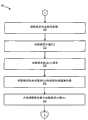
Fig. 3 A-3C is the process flow diagram that is returned the process of copying by the exemplary optimized of the accumulator system realization of Figure 1A and 1B.In some implementations,process 300 can be stored in the memory register (for example, register 110) (302) by reading of data page or leaf from the nonvolatile memory (for example, memory cell array 106) and with this data page and begin.Can check DCI (for example DCI 130) (304) for the data page in the memory register.In some implementations, DCI can be in advance be written to nonvolatile memory (for example, utilizing process 200) time first at this data page and be calculated and be stored in the memory sub-system.In other implementations, DCI can be used as independent operation or calculates as the part " in real time " of read operation.Memory sub-system can be finished (306) to peripheral control unit (for example, peripheral control unit 116) report read operation.
If the DCI of the data page in the register shows this data page and changes (308), then this data page can be sent to peripheral control unit (310), can be that this data page calculates ECC (312), and the ECC information (314) of externally proofreading and correct this data page in the controller.Data page and the ECC that is associated can be sent back memory register (316).Can calculate new DCI (318) for the data page in the memory register.
If the DCI of the data page in the register shows this data page and do not change (308), then calculate ECC (320) for the new metadata that is associated with this data page.New metadata and the ECC that is associated can be sent to memory register (322).Can calculate new DCI (324) for the metadata in the memory register.The memory register content can be written to the new data page or leaf (326) in the nonvolatile memory.
Optimize read operation
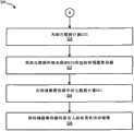
Fig. 4 is the process flow diagram by the exemplary optimized read operation of the accumulator system realization of Figure 1A and 1B.In some implementations, process 400 can be stored in that (402) begin in the memory register by reading of data page or leaf from nonvolatile memory and with this data page.The precalculated DCI that is associated with this data page can be by the memory location clock from memory sub-system in memory register and checked (404).Also can " in real time " calculate DCI.The state that can read DCI is to judge whether this data page changes (406).
If this data page changes (408), then can calculate the ECC of the new metadata that is associated with this data page and itself and this new metadata are sent to memory register (412).Can calculate new DCI and content of registers can be written to new data page or leaf (414) in the nonvolatile memory for the metadata in the memory register.
If this data page does not change (408), then the memory register content can be sent to peripheral control unit and peripheral control unit and can calculate ECC (410).Peripheral control unit can calculate the ECC of the new metadata that is associated with this data page and itself and new metadata are sent to memory register (412).Can calculate new DCI and content of registers can be written to new data page or leaf (414) in the nonvolatile memory for the metadata in the memory register.
Example data structure
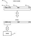
Fig. 5 shows returning of Fig. 3 A-3C and copies the employed example data structure of process.In shown example, thedata page 500 in the nonvolatile memory comprisesmetadata 502, metadata ECC504,data 506 and data ECC 508.If data do not change, then have onlymetadata 502 andmetadata ECC 504 by from the register transfer to theperipheral control unit 510 so that handle.Treatedmetadata 502 andmetadata ECC 504 are transferred back to memory sub-system and are stored in the memory register.This data page can be written to the new data page or leaf in the nonvolatile memory (for example, memory cell array).
Some implementations have been described.However, it should be understood that and to carry out various modifications.For example, the key element of one or more implementations can be combined, delete, revises or replenish to form other implementations.As another example, the logic flow shown in the accompanying drawing does not also require the result that could realize expectation by shown particular order or sequencing.In addition, can provide other steps, perhaps can from described flow process, remove step, and can add other assemblies, or from described system, remove assembly.Therefore, other implementations within the scope of the claims.
Claims (17)
1. method comprises:
Obtain data page from the nonvolatile memory of memory sub-system;
Judge whether described data page has changed; And
If described data page has changed,
Then described data page is sent to controller so that handle;
If described data page does not change,
Then described controller will be sent to the metadata that described data page is associated so that handle.
2. the method for claim 1, judge wherein whether described data page has changed also to comprise:
The data that read described data page change designator.
3. method as claimed in claim 2, wherein said data change designator and are associated with error detecting code.
4. the method for claim 1, judge wherein whether described data page has changed also to comprise:
For described data page computational data changes designator; And
Change designator based on described data and judge whether described data page has changed.
5. system comprises:
Be suitable for being coupled to the interface of controller;
Nonvolatile memory;
Be coupled to the processor of described nonvolatile memory and described interface, this processor can be operated to be used for obtaining data page from described nonvolatile memory;
Judge whether described data page has changed; And
If described data page has changed,
Then described data page is sent to described controller by described interface so that handle;
If described data page does not change,
Then the metadata that will be associated with described data page sends to described controller by described interface so that handle.
6. system as claimed in claim 5, judge wherein whether described data page has changed also to comprise:
The data that read described data page change designator.
7. system as claimed in claim 6, wherein said data change designator and are associated with error detecting code.
8. system as claimed in claim 5, judge wherein whether described data page has changed also to comprise:
For described data page computational data changes designator; And
Change designator based on described data and judge whether described data page has changed.
9. method comprises:
The metadata that obtains data page and be associated from the nonvolatile memory of the memory sub-system that is coupled to controller;
Described data page is stored in the register of described memory sub-system;
Described data page and the metadata that is associated are sent to described controller so that handle from described register;
Receive treated data page and the metadata that is associated from described controller;
Judge whether described treated data page has changed;
If described treated data page has changed,
Then described treated data page and the metadata that is associated are written to the described register in the described memory sub-system;
If described treated data page does not change,
Then the described metadata that is associated is written to the described register in the described memory sub-system; And
The content of described register is written to described nonvolatile memory.
10. method as claimed in claim 9, judge wherein whether described treated data page has changed also to comprise:
The data that read described treated data page change designator.
11. method as claimed in claim 10, wherein said data change designator and are associated with error detecting code.
12. method as claimed in claim 9 is judged wherein whether described treated data page has changed also to comprise:
For described treated data page computational data changes designator; And
Change designator based on described data and judge whether described treated data page has changed.
13. a system comprises:
Be suitable for being coupled to the interface of controller;
Nonvolatile memory;
Be coupled to the processor of described nonvolatile memory and described interface, this processor can be operated to be used for from the nonvolatile memory acquisition data page and the metadata that is associated of the memory sub-system that is coupled to described controller;
Described data page is stored in the register of described accumulator system;
Described data page and the metadata that is associated are sent to described controller by described interface so that handle from described register;
Receive treated data page and the metadata that is associated by described interface from described controller;
Judge whether described treated data page has changed;
If described treated data page has changed,
Then described treated data page and the metadata that is associated are sent to the described register in the described memory sub-system;
If described treated data page does not change,
Then treated metadata is sent to the described register in the described memory sub-system; And
The content of described register is written to described nonvolatile memory.
14. system as claimed in claim 13 judges wherein whether described treated data page has changed also to comprise:
The data that read described treated data page change designator.
15. system as claimed in claim 14, wherein said data change designator and are associated with error detecting code.
16. system as claimed in claim 13 judges wherein whether described treated data page has changed also to comprise:
For described treated data page computational data changes designator; And
Change designator based on described data and judge whether described treated data page has changed.
17. a system comprises:
Be used for obtaining the device of data page from the nonvolatile memory of memory sub-system;
Be used to judge whether altered device of described data page; And
If described data page has changed,
Be used for described data page is sent to controller so that the device of handling;
If described data page does not change,
Be used for to send to described controller with the metadata that described data page is associated so that the device of handling.
Applications Claiming Priority (5)
| Application Number | Priority Date | Filing Date | Title |
|---|---|---|---|
| US4933008P | 2008-04-30 | 2008-04-30 | |
| US61/049,330 | 2008-04-30 | ||
| US12/193,638 | 2008-08-18 | ||
| US12/193,638US8185706B2 (en) | 2008-04-30 | 2008-08-18 | Copyback optimization for memory system |
| PCT/US2009/039160WO2009134576A1 (en) | 2008-04-30 | 2009-04-01 | Copyback optimization for memory system |
Publications (2)
| Publication Number | Publication Date |
|---|---|
| CN102077176Atrue CN102077176A (en) | 2011-05-25 |
| CN102077176B CN102077176B (en) | 2013-06-19 |
Family
ID=40801795
Family Applications (1)
| Application Number | Title | Priority Date | Filing Date |
|---|---|---|---|
| CN2009801252990AExpired - Fee RelatedCN102077176B (en) | 2008-04-30 | 2009-04-01 | Copyback optimization for memory system |
Country Status (8)
| Country | Link |
|---|---|
| US (2) | US8185706B2 (en) |
| EP (2) | EP2297642B1 (en) |
| JP (1) | JP5192587B2 (en) |
| KR (2) | KR101471262B1 (en) |
| CN (1) | CN102077176B (en) |
| AT (1) | ATE535866T1 (en) |
| ES (1) | ES2378371T3 (en) |
| WO (1) | WO2009134576A1 (en) |
Families Citing this family (81)
| Publication number | Priority date | Publication date | Assignee | Title |
|---|---|---|---|---|
| US8762620B2 (en) | 2007-12-27 | 2014-06-24 | Sandisk Enterprise Ip Llc | Multiprocessor storage controller |
| US8443263B2 (en)* | 2009-12-30 | 2013-05-14 | Sandisk Technologies Inc. | Method and controller for performing a copy-back operation |
| US8365041B2 (en) | 2010-03-17 | 2013-01-29 | Sandisk Enterprise Ip Llc | MLC self-raid flash data protection scheme |
| KR101844346B1 (en)* | 2010-11-05 | 2018-04-02 | 삼성전자주식회사 | Memory system and method of operating a memory system |
| US8909982B2 (en) | 2011-06-19 | 2014-12-09 | Sandisk Enterprise Ip Llc | System and method for detecting copyback programming problems |
| US8910020B2 (en) | 2011-06-19 | 2014-12-09 | Sandisk Enterprise Ip Llc | Intelligent bit recovery for flash memory |
| US8938658B2 (en) | 2011-11-07 | 2015-01-20 | Sandisk Enterprise Ip Llc | Statistical read comparison signal generation for memory systems |
| US8954822B2 (en) | 2011-11-18 | 2015-02-10 | Sandisk Enterprise Ip Llc | Data encoder and decoder using memory-specific parity-check matrix |
| US8924815B2 (en) | 2011-11-18 | 2014-12-30 | Sandisk Enterprise Ip Llc | Systems, methods and devices for decoding codewords having multiple parity segments |
| US9048876B2 (en) | 2011-11-18 | 2015-06-02 | Sandisk Enterprise Ip Llc | Systems, methods and devices for multi-tiered error correction |
| US9699263B1 (en) | 2012-08-17 | 2017-07-04 | Sandisk Technologies Llc. | Automatic read and write acceleration of data accessed by virtual machines |
| US9501398B2 (en) | 2012-12-26 | 2016-11-22 | Sandisk Technologies Llc | Persistent storage device with NVRAM for staging writes |
| US9239751B1 (en) | 2012-12-27 | 2016-01-19 | Sandisk Enterprise Ip Llc | Compressing data from multiple reads for error control management in memory systems |
| US9612948B2 (en) | 2012-12-27 | 2017-04-04 | Sandisk Technologies Llc | Reads and writes between a contiguous data block and noncontiguous sets of logical address blocks in a persistent storage device |
| US9454420B1 (en) | 2012-12-31 | 2016-09-27 | Sandisk Technologies Llc | Method and system of reading threshold voltage equalization |
| US9003264B1 (en) | 2012-12-31 | 2015-04-07 | Sandisk Enterprise Ip Llc | Systems, methods, and devices for multi-dimensional flash RAID data protection |
| US9329928B2 (en) | 2013-02-20 | 2016-05-03 | Sandisk Enterprise IP LLC. | Bandwidth optimization in a non-volatile memory system |
| US9214965B2 (en) | 2013-02-20 | 2015-12-15 | Sandisk Enterprise Ip Llc | Method and system for improving data integrity in non-volatile storage |
| US9870830B1 (en) | 2013-03-14 | 2018-01-16 | Sandisk Technologies Llc | Optimal multilevel sensing for reading data from a storage medium |
| US9244763B1 (en) | 2013-03-15 | 2016-01-26 | Sandisk Enterprise Ip Llc | System and method for updating a reading threshold voltage based on symbol transition information |
| US9136877B1 (en) | 2013-03-15 | 2015-09-15 | Sandisk Enterprise Ip Llc | Syndrome layered decoding for LDPC codes |
| US9236886B1 (en) | 2013-03-15 | 2016-01-12 | Sandisk Enterprise Ip Llc | Universal and reconfigurable QC-LDPC encoder |
| US9009576B1 (en) | 2013-03-15 | 2015-04-14 | Sandisk Enterprise Ip Llc | Adaptive LLR based on syndrome weight |
| US9092350B1 (en) | 2013-03-15 | 2015-07-28 | Sandisk Enterprise Ip Llc | Detection and handling of unbalanced errors in interleaved codewords |
| US9367246B2 (en) | 2013-03-15 | 2016-06-14 | Sandisk Technologies Inc. | Performance optimization of data transfer for soft information generation |
| US9170941B2 (en) | 2013-04-05 | 2015-10-27 | Sandisk Enterprises IP LLC | Data hardening in a storage system |
| US10049037B2 (en) | 2013-04-05 | 2018-08-14 | Sandisk Enterprise Ip Llc | Data management in a storage system |
| US9043517B1 (en) | 2013-07-25 | 2015-05-26 | Sandisk Enterprise Ip Llc | Multipass programming in buffers implemented in non-volatile data storage systems |
| US9384126B1 (en) | 2013-07-25 | 2016-07-05 | Sandisk Technologies Inc. | Methods and systems to avoid false negative results in bloom filters implemented in non-volatile data storage systems |
| US9524235B1 (en) | 2013-07-25 | 2016-12-20 | Sandisk Technologies Llc | Local hash value generation in non-volatile data storage systems |
| US9361221B1 (en) | 2013-08-26 | 2016-06-07 | Sandisk Technologies Inc. | Write amplification reduction through reliable writes during garbage collection |
| US9639463B1 (en) | 2013-08-26 | 2017-05-02 | Sandisk Technologies Llc | Heuristic aware garbage collection scheme in storage systems |
| US9442670B2 (en) | 2013-09-03 | 2016-09-13 | Sandisk Technologies Llc | Method and system for rebalancing data stored in flash memory devices |
| US9519577B2 (en) | 2013-09-03 | 2016-12-13 | Sandisk Technologies Llc | Method and system for migrating data between flash memory devices |
| US9158349B2 (en) | 2013-10-04 | 2015-10-13 | Sandisk Enterprise Ip Llc | System and method for heat dissipation |
| US9323637B2 (en) | 2013-10-07 | 2016-04-26 | Sandisk Enterprise Ip Llc | Power sequencing and data hardening architecture |
| US9442662B2 (en) | 2013-10-18 | 2016-09-13 | Sandisk Technologies Llc | Device and method for managing die groups |
| US9298608B2 (en) | 2013-10-18 | 2016-03-29 | Sandisk Enterprise Ip Llc | Biasing for wear leveling in storage systems |
| US9436831B2 (en) | 2013-10-30 | 2016-09-06 | Sandisk Technologies Llc | Secure erase in a memory device |
| US9263156B2 (en) | 2013-11-07 | 2016-02-16 | Sandisk Enterprise Ip Llc | System and method for adjusting trip points within a storage device |
| US9244785B2 (en) | 2013-11-13 | 2016-01-26 | Sandisk Enterprise Ip Llc | Simulated power failure and data hardening |
| US9152555B2 (en) | 2013-11-15 | 2015-10-06 | Sandisk Enterprise IP LLC. | Data management with modular erase in a data storage system |
| US9703816B2 (en) | 2013-11-19 | 2017-07-11 | Sandisk Technologies Llc | Method and system for forward reference logging in a persistent datastore |
| US9520197B2 (en) | 2013-11-22 | 2016-12-13 | Sandisk Technologies Llc | Adaptive erase of a storage device |
| US9122636B2 (en) | 2013-11-27 | 2015-09-01 | Sandisk Enterprise Ip Llc | Hard power fail architecture |
| US9280429B2 (en) | 2013-11-27 | 2016-03-08 | Sandisk Enterprise Ip Llc | Power fail latching based on monitoring multiple power supply voltages in a storage device |
| US9520162B2 (en) | 2013-11-27 | 2016-12-13 | Sandisk Technologies Llc | DIMM device controller supervisor |
| US9582058B2 (en) | 2013-11-29 | 2017-02-28 | Sandisk Technologies Llc | Power inrush management of storage devices |
| US9250676B2 (en) | 2013-11-29 | 2016-02-02 | Sandisk Enterprise Ip Llc | Power failure architecture and verification |
| US9092370B2 (en) | 2013-12-03 | 2015-07-28 | Sandisk Enterprise Ip Llc | Power failure tolerant cryptographic erase |
| US9235245B2 (en) | 2013-12-04 | 2016-01-12 | Sandisk Enterprise Ip Llc | Startup performance and power isolation |
| US9129665B2 (en) | 2013-12-17 | 2015-09-08 | Sandisk Enterprise Ip Llc | Dynamic brownout adjustment in a storage device |
| US9549457B2 (en) | 2014-02-12 | 2017-01-17 | Sandisk Technologies Llc | System and method for redirecting airflow across an electronic assembly |
| US9703636B2 (en) | 2014-03-01 | 2017-07-11 | Sandisk Technologies Llc | Firmware reversion trigger and control |
| US9519319B2 (en) | 2014-03-14 | 2016-12-13 | Sandisk Technologies Llc | Self-supporting thermal tube structure for electronic assemblies |
| US9485851B2 (en) | 2014-03-14 | 2016-11-01 | Sandisk Technologies Llc | Thermal tube assembly structures |
| US9348377B2 (en) | 2014-03-14 | 2016-05-24 | Sandisk Enterprise Ip Llc | Thermal isolation techniques |
| US9448876B2 (en) | 2014-03-19 | 2016-09-20 | Sandisk Technologies Llc | Fault detection and prediction in storage devices |
| US9390814B2 (en) | 2014-03-19 | 2016-07-12 | Sandisk Technologies Llc | Fault detection and prediction for data storage elements |
| US9454448B2 (en) | 2014-03-19 | 2016-09-27 | Sandisk Technologies Llc | Fault testing in storage devices |
| US9626399B2 (en) | 2014-03-31 | 2017-04-18 | Sandisk Technologies Llc | Conditional updates for reducing frequency of data modification operations |
| US9390021B2 (en) | 2014-03-31 | 2016-07-12 | Sandisk Technologies Llc | Efficient cache utilization in a tiered data structure |
| US9626400B2 (en) | 2014-03-31 | 2017-04-18 | Sandisk Technologies Llc | Compaction of information in tiered data structure |
| US9697267B2 (en) | 2014-04-03 | 2017-07-04 | Sandisk Technologies Llc | Methods and systems for performing efficient snapshots in tiered data structures |
| US8891303B1 (en) | 2014-05-30 | 2014-11-18 | Sandisk Technologies Inc. | Method and system for dynamic word line based configuration of a three-dimensional memory device |
| US9093160B1 (en) | 2014-05-30 | 2015-07-28 | Sandisk Technologies Inc. | Methods and systems for staggered memory operations |
| US10162748B2 (en) | 2014-05-30 | 2018-12-25 | Sandisk Technologies Llc | Prioritizing garbage collection and block allocation based on I/O history for logical address regions |
| US10372613B2 (en) | 2014-05-30 | 2019-08-06 | Sandisk Technologies Llc | Using sub-region I/O history to cache repeatedly accessed sub-regions in a non-volatile storage device |
| US10656840B2 (en) | 2014-05-30 | 2020-05-19 | Sandisk Technologies Llc | Real-time I/O pattern recognition to enhance performance and endurance of a storage device |
| US9645749B2 (en) | 2014-05-30 | 2017-05-09 | Sandisk Technologies Llc | Method and system for recharacterizing the storage density of a memory device or a portion thereof |
| US9703491B2 (en) | 2014-05-30 | 2017-07-11 | Sandisk Technologies Llc | Using history of unaligned writes to cache data and avoid read-modify-writes in a non-volatile storage device |
| US9070481B1 (en) | 2014-05-30 | 2015-06-30 | Sandisk Technologies Inc. | Internal current measurement for age measurements |
| US10114557B2 (en) | 2014-05-30 | 2018-10-30 | Sandisk Technologies Llc | Identification of hot regions to enhance performance and endurance of a non-volatile storage device |
| US10656842B2 (en) | 2014-05-30 | 2020-05-19 | Sandisk Technologies Llc | Using history of I/O sizes and I/O sequences to trigger coalesced writes in a non-volatile storage device |
| US10146448B2 (en) | 2014-05-30 | 2018-12-04 | Sandisk Technologies Llc | Using history of I/O sequences to trigger cached read ahead in a non-volatile storage device |
| US9652381B2 (en) | 2014-06-19 | 2017-05-16 | Sandisk Technologies Llc | Sub-block garbage collection |
| US9443601B2 (en) | 2014-09-08 | 2016-09-13 | Sandisk Technologies Llc | Holdup capacitor energy harvesting |
| CN108600043A (en)* | 2018-04-02 | 2018-09-28 | 郑州云海信息技术有限公司 | The method of Connection Service device and control terminal, server Memory function module test methods |
| US11556267B2 (en) | 2020-08-31 | 2023-01-17 | Micron Technology, Inc. | Data management during a copyback operation |
| US11533064B2 (en)* | 2020-11-09 | 2022-12-20 | Micron Technology, Inc. | Error correcting code poisoning for memory devices and associated methods and systems |
| US11436142B1 (en)* | 2021-04-23 | 2022-09-06 | EMC IP Holding Company, LLC | System and method for moving metadata without updating references used by the metadata |
Citations (3)
| Publication number | Priority date | Publication date | Assignee | Title |
|---|---|---|---|---|
| US20040049632A1 (en)* | 2002-09-09 | 2004-03-11 | Chang Albert H. | Memory controller interface with XOR operations on memory read to accelerate RAID operations |
| US20070048715A1 (en)* | 2004-12-21 | 2007-03-01 | International Business Machines Corporation | Subtitle generation and retrieval combining document processing with voice processing |
| US20070268905A1 (en)* | 2006-05-18 | 2007-11-22 | Sigmatel, Inc. | Non-volatile memory error correction system and method |
Family Cites Families (19)
| Publication number | Priority date | Publication date | Assignee | Title |
|---|---|---|---|---|
| US4020466A (en) | 1974-07-05 | 1977-04-26 | Ibm Corporation | Memory hierarchy system with journaling and copy back |
| FR2292803A1 (en)* | 1974-11-29 | 1976-06-25 | Nord Ressorts | ELASTIC DEVICE FOR RAIL FIXING AND RAIL FIXING SYSTEM WITH APPLICATION |
| US5555379A (en) | 1994-07-06 | 1996-09-10 | Advanced Micro Devices, Inc. | Cache controller index address generator |
| US5732275A (en)* | 1996-01-11 | 1998-03-24 | Apple Computer, Inc. | Method and apparatus for managing and automatically updating software programs |
| JPH11259357A (en)* | 1998-03-09 | 1999-09-24 | Seiko Epson Corp | Semiconductor integrated device and nonvolatile memory writing method |
| JP3376331B2 (en)* | 1999-11-25 | 2003-02-10 | エヌイーシーアクセステクニカ株式会社 | Storage method using flash memory and storage medium storing storage control program |
| US6601216B1 (en) | 2000-03-31 | 2003-07-29 | Microsoft Corporation | Differential cyclic redundancy check |
| US7350044B2 (en)* | 2004-01-30 | 2008-03-25 | Micron Technology, Inc. | Data move method and apparatus |
| US7287209B2 (en)* | 2004-06-03 | 2007-10-23 | Cheertek, Inc. | System and method for detecting codeword errors in error correction code or cyclic redundancy check code |
| US7466597B2 (en) | 2004-09-09 | 2008-12-16 | Samsung Electronics Co., Ltd. | NAND flash memory device and copyback program method for same |
| TWI258074B (en) | 2004-12-24 | 2006-07-11 | Phison Electronics Corp | Method for reducing data error when flash memory storage device executing copy back command |
| JP4688584B2 (en)* | 2005-06-21 | 2011-05-25 | 株式会社日立製作所 | Storage device |
| US7362611B2 (en) | 2005-08-30 | 2008-04-22 | Micron Technology, Inc. | Non-volatile memory copy back |
| US7512864B2 (en)* | 2005-09-30 | 2009-03-31 | Josef Zeevi | System and method of accessing non-volatile computer memory |
| JP4956230B2 (en)* | 2006-04-10 | 2012-06-20 | 株式会社東芝 | Memory controller |
| US20070276863A1 (en) | 2006-05-02 | 2007-11-29 | Research In Motion Limited | Plug in registration method and apparatus for push content delivery |
| JP2007310680A (en)* | 2006-05-18 | 2007-11-29 | Matsushita Electric Ind Co Ltd | Nonvolatile storage device and data transfer method thereof |
| KR100881669B1 (en)* | 2006-12-18 | 2009-02-06 | 삼성전자주식회사 | Static data area detection method, wear leveling method, data unit merging method and non-volatile data storage device |
| US20080288712A1 (en)* | 2007-04-25 | 2008-11-20 | Cornwell Michael J | Accessing metadata with an external host |
- 2008
- 2008-08-18USUS12/193,638patent/US8185706B2/ennot_activeExpired - Fee Related
- 2009
- 2009-04-01KRKR1020127013247Apatent/KR101471262B1/ennot_activeExpired - Fee Related
- 2009-04-01EPEP09739378Apatent/EP2297642B1/enactiveActive
- 2009-04-01ATAT09739378Tpatent/ATE535866T1/enactive
- 2009-04-01WOPCT/US2009/039160patent/WO2009134576A1/enactiveApplication Filing
- 2009-04-01EPEP11183929.6Apatent/EP2407883B1/ennot_activeNot-in-force
- 2009-04-01CNCN2009801252990Apatent/CN102077176B/ennot_activeExpired - Fee Related
- 2009-04-01ESES09739378Tpatent/ES2378371T3/enactiveActive
- 2009-04-01JPJP2011507514Apatent/JP5192587B2/ennot_activeExpired - Fee Related
- 2009-04-01KRKR1020107026742Apatent/KR101225924B1/ennot_activeExpired - Fee Related
- 2012
- 2012-05-21USUS13/476,605patent/US8572335B2/enactiveActive
Patent Citations (3)
| Publication number | Priority date | Publication date | Assignee | Title |
|---|---|---|---|---|
| US20040049632A1 (en)* | 2002-09-09 | 2004-03-11 | Chang Albert H. | Memory controller interface with XOR operations on memory read to accelerate RAID operations |
| US20070048715A1 (en)* | 2004-12-21 | 2007-03-01 | International Business Machines Corporation | Subtitle generation and retrieval combining document processing with voice processing |
| US20070268905A1 (en)* | 2006-05-18 | 2007-11-22 | Sigmatel, Inc. | Non-volatile memory error correction system and method |
Also Published As
| Publication number | Publication date |
|---|---|
| HK1155530A1 (en) | 2012-05-18 |
| EP2297642B1 (en) | 2011-11-30 |
| KR101225924B1 (en) | 2013-01-24 |
| US20090276560A1 (en) | 2009-11-05 |
| US20120233387A1 (en) | 2012-09-13 |
| EP2407883A1 (en) | 2012-01-18 |
| KR20110008301A (en) | 2011-01-26 |
| KR101471262B1 (en) | 2014-12-10 |
| EP2297642A1 (en) | 2011-03-23 |
| ATE535866T1 (en) | 2011-12-15 |
| KR20120059658A (en) | 2012-06-08 |
| HK1158344A1 (en) | 2012-07-13 |
| US8185706B2 (en) | 2012-05-22 |
| US8572335B2 (en) | 2013-10-29 |
| WO2009134576A1 (en) | 2009-11-05 |
| JP5192587B2 (en) | 2013-05-08 |
| HK1166390A1 (en) | 2012-10-26 |
| EP2407883B1 (en) | 2013-08-21 |
| ES2378371T3 (en) | 2012-04-11 |
| CN102077176B (en) | 2013-06-19 |
| JP2011520188A (en) | 2011-07-14 |
Similar Documents
| Publication | Publication Date | Title |
|---|---|---|
| CN102077176B (en) | Copyback optimization for memory system | |
| CN110858129B (en) | Data storage device and method of operation thereof | |
| KR101491943B1 (en) | Transaction log recovery | |
| US10963160B2 (en) | Apparatus and method for checking valid data in block capable of storing large volume data in memory system | |
| US20200089566A1 (en) | Apparatus for diagnosing memory system and operating method thereof | |
| CN101901169B (en) | Scanner and method | |
| CN106557432B (en) | Buffer memory management method, memory control circuit unit and storage device | |
| CN113900586A (en) | Memory system and operating method thereof | |
| US11288015B2 (en) | Memory system for accurately predicting power required for sequential command operations performed in memory device, and operation method thereof | |
| US20210157723A1 (en) | Memory system and operation method thereof | |
| CN102981969A (en) | Method for deleting repeated data and solid hard disc thereof | |
| US10289328B2 (en) | Memory controller and method for handling host request based on data character | |
| US11314653B2 (en) | Memory controller | |
| US11354051B2 (en) | Memory system for efficiently managing memory block and operating method thereof | |
| CN113849121A (en) | Memory system for accessing stripe form data and operating method thereof | |
| TWI436209B (en) | Memory management table proceesing method, memory controller and memory storage apparatus | |
| CN117389461A (en) | memory device | |
| CN112433668A (en) | Memory system and data processing system for predicting whether internal operation is executable | |
| CN106980464B (en) | System optimization method using oversampled reads | |
| HK1158344B (en) | Copyback optimization for memory system | |
| HK1155530B (en) | Copyback optimization for memory system | |
| CN120295580A (en) | Memory control method and storage device | |
| HK1166390B (en) | Copyback optimization for memory system | |
| CN120406845A (en) | Memory management method and storage device | |
| CN120406850A (en) | Data access method and storage device |
Legal Events
| Date | Code | Title | Description |
|---|---|---|---|
| C06 | Publication | ||
| PB01 | Publication | ||
| C10 | Entry into substantive examination | ||
| SE01 | Entry into force of request for substantive examination | ||
| REG | Reference to a national code | Ref country code:HK Ref legal event code:DE Ref document number:1158344 Country of ref document:HK | |
| C14 | Grant of patent or utility model | ||
| GR01 | Patent grant | ||
| REG | Reference to a national code | Ref country code:HK Ref legal event code:GR Ref document number:1158344 Country of ref document:HK | |
| CF01 | Termination of patent right due to non-payment of annual fee | ||
| CF01 | Termination of patent right due to non-payment of annual fee | Granted publication date:20130619 |