CN102076602B - Method for encapsulating a display device and device obtained therefrom - Google Patents
Method for encapsulating a display device and device obtained therefromDownload PDFInfo
- Publication number
- CN102076602B CN102076602BCN200980124408.7ACN200980124408ACN102076602BCN 102076602 BCN102076602 BCN 102076602BCN 200980124408 ACN200980124408 ACN 200980124408ACN 102076602 BCN102076602 BCN 102076602B
- Authority
- CN
- China
- Prior art keywords
- transparent substrates
- backboard
- display device
- display
- display element
- Prior art date
- Legal status (The legal status is an assumption and is not a legal conclusion. Google has not performed a legal analysis and makes no representation as to the accuracy of the status listed.)
- Expired - Fee Related
Links
Images


Classifications
- G—PHYSICS
- G09—EDUCATION; CRYPTOGRAPHY; DISPLAY; ADVERTISING; SEALS
- G09G—ARRANGEMENTS OR CIRCUITS FOR CONTROL OF INDICATING DEVICES USING STATIC MEANS TO PRESENT VARIABLE INFORMATION
- G09G3/00—Control arrangements or circuits, of interest only in connection with visual indicators other than cathode-ray tubes
- G09G3/20—Control arrangements or circuits, of interest only in connection with visual indicators other than cathode-ray tubes for presentation of an assembly of a number of characters, e.g. a page, by composing the assembly by combination of individual elements arranged in a matrix no fixed position being assigned to or needed to be assigned to the individual characters or partial characters
- G09G3/34—Control arrangements or circuits, of interest only in connection with visual indicators other than cathode-ray tubes for presentation of an assembly of a number of characters, e.g. a page, by composing the assembly by combination of individual elements arranged in a matrix no fixed position being assigned to or needed to be assigned to the individual characters or partial characters by control of light from an independent source
- G09G3/3433—Control arrangements or circuits, of interest only in connection with visual indicators other than cathode-ray tubes for presentation of an assembly of a number of characters, e.g. a page, by composing the assembly by combination of individual elements arranged in a matrix no fixed position being assigned to or needed to be assigned to the individual characters or partial characters by control of light from an independent source using light modulating elements actuated by an electric field and being other than liquid crystal devices and electrochromic devices
- G09G3/3466—Control arrangements or circuits, of interest only in connection with visual indicators other than cathode-ray tubes for presentation of an assembly of a number of characters, e.g. a page, by composing the assembly by combination of individual elements arranged in a matrix no fixed position being assigned to or needed to be assigned to the individual characters or partial characters by control of light from an independent source using light modulating elements actuated by an electric field and being other than liquid crystal devices and electrochromic devices based on interferometric effect
- H—ELECTRICITY
- H10—SEMICONDUCTOR DEVICES; ELECTRIC SOLID-STATE DEVICES NOT OTHERWISE PROVIDED FOR
- H10H—INORGANIC LIGHT-EMITTING SEMICONDUCTOR DEVICES HAVING POTENTIAL BARRIERS
- H10H20/00—Individual inorganic light-emitting semiconductor devices having potential barriers, e.g. light-emitting diodes [LED]
- H10H20/80—Constructional details
- B—PERFORMING OPERATIONS; TRANSPORTING
- B81—MICROSTRUCTURAL TECHNOLOGY
- B81C—PROCESSES OR APPARATUS SPECIALLY ADAPTED FOR THE MANUFACTURE OR TREATMENT OF MICROSTRUCTURAL DEVICES OR SYSTEMS
- B81C1/00—Manufacture or treatment of devices or systems in or on a substrate
- B81C1/00015—Manufacture or treatment of devices or systems in or on a substrate for manufacturing microsystems
- B81C1/00261—Processes for packaging MEMS devices
- B81C1/00317—Packaging optical devices
- G—PHYSICS
- G02—OPTICS
- G02B—OPTICAL ELEMENTS, SYSTEMS OR APPARATUS
- G02B26/00—Optical devices or arrangements for the control of light using movable or deformable optical elements
- G02B26/001—Optical devices or arrangements for the control of light using movable or deformable optical elements based on interference in an adjustable optical cavity
- B—PERFORMING OPERATIONS; TRANSPORTING
- B81—MICROSTRUCTURAL TECHNOLOGY
- B81B—MICROSTRUCTURAL DEVICES OR SYSTEMS, e.g. MICROMECHANICAL DEVICES
- B81B2201/00—Specific applications of microelectromechanical systems
- B81B2201/04—Optical MEMS
- B81B2201/047—Optical MEMS not provided for in B81B2201/042 - B81B2201/045
- B—PERFORMING OPERATIONS; TRANSPORTING
- B81—MICROSTRUCTURAL TECHNOLOGY
- B81C—PROCESSES OR APPARATUS SPECIALLY ADAPTED FOR THE MANUFACTURE OR TREATMENT OF MICROSTRUCTURAL DEVICES OR SYSTEMS
- B81C2203/00—Forming microstructural systems
- B81C2203/01—Packaging MEMS
- B81C2203/0118—Bonding a wafer on the substrate, i.e. where the cap consists of another wafer
- B—PERFORMING OPERATIONS; TRANSPORTING
- B81—MICROSTRUCTURAL TECHNOLOGY
- B81C—PROCESSES OR APPARATUS SPECIALLY ADAPTED FOR THE MANUFACTURE OR TREATMENT OF MICROSTRUCTURAL DEVICES OR SYSTEMS
- B81C2203/00—Forming microstructural systems
- B81C2203/05—Aligning components to be assembled
- B81C2203/051—Active alignment, e.g. using internal or external actuators, magnets, sensors, marks or marks detectors
- Y—GENERAL TAGGING OF NEW TECHNOLOGICAL DEVELOPMENTS; GENERAL TAGGING OF CROSS-SECTIONAL TECHNOLOGIES SPANNING OVER SEVERAL SECTIONS OF THE IPC; TECHNICAL SUBJECTS COVERED BY FORMER USPC CROSS-REFERENCE ART COLLECTIONS [XRACs] AND DIGESTS
- Y10—TECHNICAL SUBJECTS COVERED BY FORMER USPC
- Y10T—TECHNICAL SUBJECTS COVERED BY FORMER US CLASSIFICATION
- Y10T29/00—Metal working
- Y10T29/49—Method of mechanical manufacture
- Y10T29/49002—Electrical device making
- Y10T29/49117—Conductor or circuit manufacturing
- Y10T29/49124—On flat or curved insulated base, e.g., printed circuit, etc.
Landscapes
- Engineering & Computer Science (AREA)
- Physics & Mathematics (AREA)
- General Physics & Mathematics (AREA)
- Microelectronics & Electronic Packaging (AREA)
- Manufacturing & Machinery (AREA)
- Computer Hardware Design (AREA)
- Theoretical Computer Science (AREA)
- Spectroscopy & Molecular Physics (AREA)
- Optics & Photonics (AREA)
- Mechanical Light Control Or Optical Switches (AREA)
- Micromachines (AREA)
- Devices For Indicating Variable Information By Combining Individual Elements (AREA)
Abstract
Description
Translated fromChinese技术领域technical field
本发明的领域涉及微机电系统(MEMS)。The field of the invention relates to microelectromechanical systems (MEMS).
背景技术Background technique
微机电系统(MEMS)包含微机械元件、致动器和电子元件。可使用沉积、蚀刻和/或其它蚀刻掉衬底和/或已沉积材料层的若干部分或者添加层以形成电装置和机电装置的微加工工艺来产生微机械元件。一种类型的MEMS装置称为干涉式调制器。如本文所使用,术语干涉式调制器或干涉式光调制器指的是一种使用光学干涉原理选择性地吸收和/或反射光的装置。在某些实施例中,干涉式调制器可包括一对导电板,其中之一或两者可能整体或部分透明且/或具有反射性,且能够在施加适当电信号后即刻进行相对运动。在特定实施例中,一个板可包括沉积在衬底上的固定层,且另一个板可包括通过气隙与固定层分离的金属薄膜。如本文更详细地描述,一个板相对于另一个板的位置可改变入射在干涉式调制器上的光的光学干涉。此些装置具有广范围的应用,且在此项技术中,利用且/或修改这些类型的装置的特性以使得其特征可被发掘用于改进现有产品和创造尚未开发的新产品将是有益的。Microelectromechanical systems (MEMS) contain micromechanical elements, actuators, and electronics. Micromechanical elements may be produced using deposition, etching, and/or other micromachining processes that etch away portions of substrates and/or deposited material layers, or add layers to form electrical and electromechanical devices. One type of MEMS device is called an interferometric modulator. As used herein, the term interferometric modulator or interferometric light modulator refers to a device that selectively absorbs and/or reflects light using the principles of optical interference. In some embodiments, an interferometric modulator may include a pair of conductive plates, one or both of which may be transparent and/or reflective in whole or in part, and capable of relative motion upon application of an appropriate electrical signal. In a particular embodiment, one plate may include a pinned layer deposited on a substrate, and the other plate may include a thin metal film separated from the pinned layer by an air gap. As described in more detail herein, the position of one plate relative to another can alter the optical interference of light incident on the interferometric modulator. Such devices have a wide range of applications and it would be beneficial in the art to exploit and/or modify the properties of these types of devices so that their characteristics can be exploited to improve existing products and create new ones that have yet to be developed of.
发明内容Contents of the invention
本发明的系统、方法和装置各自具有若干方面,其中无单个方面单独地负责其所要属性。在不限制本发明的范围的情况下,现在将简要地论述本发明的较显著特征。在考虑此论述之后,且尤其在阅读标题为“具体实施方式”的部分之后,将理解本发明的特征如何提供优于其它显示装置的优点。The systems, methods, and devices of the invention each have several aspects, no single one of which is solely responsible for its desirable attributes. Without limiting the scope of the invention, the more salient features of the invention will now be briefly discussed. After considering this discussion, and particularly after reading the section entitled "Detailed Description of Preferred Embodiments," one will understand how the features of this invention provide advantages over other display devices.
在一个方面中,揭示一种封装显示装置的方法。所述方法包括:提供衬底;在所述衬底的背侧上制造显示元件阵列,所述阵列包括位于所述显示元件之间的连接所述显示元件的电极的多个柱;提供背板;以及将所述背板密封到所述衬底的所述背侧,其中在将所述背板密封到所述衬底的所述背侧之后,一个或一个以上柱与所述背板接触。In one aspect, a method of packaging a display device is disclosed. The method includes: providing a substrate; fabricating an array of display elements on the backside of the substrate, the array including a plurality of posts between the display elements connecting electrodes of the display elements; providing a backplane and sealing the backplate to the backside of the substrate, wherein one or more posts contact the backplate after sealing the backplate to the backside of the substrate .
在另一方面中,揭示一种封装显示装置的方法。所述方法包括:提供衬底;在所述衬底的背侧上制造显示元件阵列,所述阵列包括位于所述显示元件之间的合适的焊盘焊接区域以及位于所述显示元件之间的连接所述显示元件的电极的多个柱;提供背板,其包括多个支柱;以及通过使所述支柱与所述焊盘焊接区域对准来将所述背板密封到所述衬底的所述背侧。In another aspect, a method of packaging a display device is disclosed. The method includes: providing a substrate; fabricating an array of display elements on the backside of the substrate, the array including suitable pad bonding regions between the display elements and bonding pads between the display elements. a plurality of pillars connecting electrodes of the display elements; providing a backplane comprising a plurality of pillars; and sealing the backplane to the substrate by aligning the pillars with the pad bonding areas the dorsal side.
在另一方面中,揭示一种封装显示装置的方法。所述方法包括:提供衬底;在所述衬底的背侧上制造显示元件阵列,所述阵列包括位于所述显示元件之间的多个支柱以及位于所述显示元件之间的连接所述显示元件的电极的多个连接柱;提供背板;以及将所述背板密封到所述衬底的所述背侧。In another aspect, a method of packaging a display device is disclosed. The method includes: providing a substrate; fabricating an array of display elements on the backside of the substrate, the array including a plurality of pillars between the display elements and connecting elements between the display elements. A plurality of connection posts for electrodes of a display element; providing a backplane; and sealing the backplane to the backside of the substrate.
在另一方面中,揭示一种显示装置。所述装置包括:前面板,其包括位于衬底的背侧上的显示元件阵列,所述阵列包括位于所述显示元件之间的连接所述显示元件的电极的多个柱,其中一个或一个以上柱与所述背板接触;以及背板,其密封到所述衬底的所述背侧。In another aspect, a display device is disclosed. The device includes a front panel comprising an array of display elements on the backside of a substrate, the array comprising a plurality of posts between the display elements connecting electrodes of the display elements, one or The above posts are in contact with the backplate; and a backplate sealed to the backside of the substrate.
在另一方面中,揭示一种显示装置。所述装置包括:前面板,其包括位于衬底的背侧上的显示元件阵列,所述阵列包括位于所述显示元件之间的合适的焊盘焊接区域以及位于所述显示元件之间的连接所述显示元件的电极的多个柱;以及背板,其密封到所述衬底的所述背侧,所述背板包括多个支柱。In another aspect, a display device is disclosed. The device includes a front panel comprising an array of display elements on the backside of the substrate, the array including suitable pad bonding areas between the display elements and connections between the display elements a plurality of posts of electrodes of the display element; and a backplate sealed to the backside of the substrate, the backplate including a plurality of posts.
在另一方面中,揭示一种显示装置。所述装置包括:前面板,其包括位于衬底的背侧上的显示元件阵列,所述阵列包括位于所述显示元件之间的多个支柱以及位于所述显示元件之间的连接所述显示元件的电极的多个连接柱;以及背板,其密封到所述衬底的所述背侧。In another aspect, a display device is disclosed. The device includes a front panel including an array of display elements on the backside of a substrate, the array including a plurality of pillars between the display elements and connecting the display elements between the display elements. a plurality of connection posts for electrodes of a component; and a backplate sealed to the backside of the substrate.
在另一方面中,揭示一种显示装置。所述装置包括:用于调制透射穿过所述支撑装置的光的装置;用于支撑所述调制装置的装置;用于封闭所述调制装置的装置;以及用于在所述封闭装置接合到所述支撑装置以形成封装时对所述封闭装置提供支撑的装置。In another aspect, a display device is disclosed. Said means comprises: means for modulating light transmitted through said supporting means; means for supporting said modulating means; means for enclosing said modulating means; The supporting means is a means for supporting the closing means when forming the package.
附图说明Description of drawings
图1是描绘干涉式调制器显示器的一个实施例的一部分的等角视图,其中第一干涉式调制器的可移动反射层处于松弛位置,且第二干涉式调制器的可移动反射层处于致动位置。FIG. 1 is an isometric view depicting a portion of one embodiment of an interferometric modulator display with the movable reflective layer of a first interferometric modulator in a relaxed position and the movable reflective layer of a second interferometric modulator in an induced position. move position.
图2是说明并入有3×3干涉式调制器显示器的电子装置的一个实施例的系统框图。Figure 2 is a system block diagram illustrating one embodiment of an electronic device incorporating a 3x3 interferometric modulator display.
图3是图1的干涉式调制器的一个示范性实施例的可移动镜位置对所施加电压的图。3 is a graph of movable mirror position versus applied voltage for one exemplary embodiment of the interferometric modulator of FIG. 1 .
图4是可用于驱动干涉式调制器显示器的一组行和列电压的说明。Figure 4 is an illustration of a set of row and column voltages that can be used to drive an interferometric modulator display.
图5A说明图2的3×3干涉式调制器显示器中的显示器数据的一个示范性帧。5A illustrates one exemplary frame of display data in the 3x3 interferometric modulator display of FIG. 2 .
图5B说明可用于写入图5A的帧的行和列信号的一个示范性时序图。FIG. 5B illustrates an exemplary timing diagram of row and column signals that may be used to write the frame of FIG. 5A.
图6A和图6B是说明包括多个干涉式调制器的视觉显示装置的实施例的系统框图。6A and 6B are system block diagrams illustrating embodiments of a visual display device including multiple interferometric modulators.
图7A是图1的装置的横截面。FIG. 7A is a cross-section of the device of FIG. 1 .
图7B是干涉式调制器的替代实施例的横截面。Figure 7B is a cross-section of an alternate embodiment of an interferometric modulator.
图7C是干涉式调制器的另一替代实施例的横截面。Figure 7C is a cross-section of another alternative embodiment of an interferometric modulator.
图7D是干涉式调制器的又一替代实施例的横截面。Figure 7D is a cross-section of yet another alternative embodiment of an interferometric modulator.
图7E是干涉式调制器的额外替代实施例的横截面。Figure 7E is a cross-section of an additional alternative embodiment of an interferometric modulator.
图8A和图8B展示在封装中包括干涉式调制器阵列的显示器的实施例的侧视图。8A and 8B show side views of an embodiment of a display including an array of interferometric modulators in a package.
图9A和图9B展示在封装中包括干涉式调制器阵列的显示器的实施例的侧视图。9A and 9B show side views of an embodiment of a display including an array of interferometric modulators in a package.
图10A和图10B展示在封装中包括干涉式调制器阵列的显示器的实施例的侧视图。10A and 10B show side views of an embodiment of a display including an array of interferometric modulators in a package.
具体实施方式Detailed ways
以下详细描述针对本发明的某些特定实施例。然而,本发明可以许多不同方式体现。在本描述内容中参看了附图,附图中所有相同部分用相同标号表示。如从以下描述中将了解,所述实施例可实施在经配置以显示不论运动(例如,视频)还是固定(例如,静止图像)的且不论文字还是图画的图像的任何装置中。更明确地说,预期所述实施例可实施在多种电子装置中或与多种电子装置关联,所述多种电子装置例如(但不限于)移动电话、无线装置、个人数据助理(PDA)、手持式或便携式计算机、GPS接收器/导航器、相机、MP3播放器、摄像机、游戏控制台、手表、时钟、计算器、电视监视器、平板显示器、计算机监视器、汽车显示器(例如,里程表显示器等)、座舱控制器和/或显示器、相机视图的显示器(例如,车辆中后视相机的显示器)、电子相片、电子广告牌或指示牌、投影仪、建筑结构、包装和美学结构(例如,一件珠宝上的图像显示器)。具有与本文中描述的装置类似的结构的MEMS装置也可用于例如电子切换装置的非显示器应用中。The following detailed description is directed to certain specific embodiments of the invention. However, the invention can be embodied in many different ways. Throughout this description reference is made to the drawings in which all like parts are designated by like numerals. As will be appreciated from the following description, the embodiments may be implemented in any device configured to display images, whether in motion (eg, video) or stationary (eg, still images), and whether textual or pictorial. More specifically, it is contemplated that the described embodiments may be implemented in or associated with a variety of electronic devices such as, but not limited to, mobile phones, wireless devices, personal data assistants (PDAs) , handheld or portable computers, GPS receivers/navigators, cameras, MP3 players, video cameras, game consoles, watches, clocks, calculators, television monitors, flat panel displays, computer monitors, automotive displays (e.g., mileage dashboard displays, etc.), cockpit controls and/or displays, camera view displays (e.g., rear view camera displays in vehicles), electronic photographs, electronic billboards or signage, projectors, architectural structures, packaging and aesthetic structures ( For example, an image display on a piece of jewelry). MEMS devices having structures similar to those described herein may also be used in non-display applications such as electronic switching devices.
下文将描述的某些实施例涉及一种封装MEMS显示装置的方法及其所获得的装置。在一个实施例中,所述装置是通过将背板接合到上面包含干涉式调制器阵列的衬底来形成的。封装中包含各种结构以保持背板与衬底之间的最小距离。Certain embodiments to be described below relate to a method of packaging a MEMS display device and the device obtained therefrom. In one embodiment, the device is formed by bonding a backplate to a substrate containing an array of interferometric modulators thereon. Various structures are included in the package to maintain a minimum distance between the backplane and the substrate.
图1中说明包括干涉式MEMS显示元件的一个干涉式调制器显示器的实施例。在这些装置中,像素处于明亮状态或黑暗状态。在明亮(“接通”或“开启”)状态下,显示元件将入射可见光的大部分反射到用户。当在黑暗(“断开”或“关闭”)状态下时,显示元件将极少的入射可见光反射到用户。依据实施例而定,可颠倒“接通”和“断开”状态的光反射特性。MEMS像素可经配置以主要在所选颜色下反射,从而除了黑色和白色以外还允许彩色显示器。An embodiment of an interferometric modulator display comprising interferometric MEMS display elements is illustrated in FIG. 1 . In these devices, pixels are either in a bright state or a dark state. In the bright ("on" or "on") state, the display element reflects a substantial portion of incident visible light to the user. When in the dark ("off" or "off") state, the display element reflects very little incident visible light to the user. Depending on the embodiment, the light reflection characteristics of the "on" and "off" states may be reversed. MEMS pixels can be configured to reflect primarily at selected colors, allowing color displays in addition to black and white.
图1是描述视觉显示器的一系列像素中的两个邻近像素的等角视图,其中每一像素包括MEMS干涉式调制器。在一些实施例中,干涉式调制器显示器包括这些干涉式调制器的行/列阵列。每一干涉式调制器包含一对反射层,其定位成彼此相距可变且可控制的距离以形成具有至少一个可变尺寸的谐振光学间隙。在一个实施例中,可在两个位置之间移动所述反射层之一。在第一位置(本文中称为松弛位置)中,可移动反射层定位成距固定部分反射层相对较大的距离。在第二位置(本文中称为致动位置)中,可移动反射层定位成更紧密邻近所述部分反射层。视可移动反射层的位置而定,从所述两个层反射的入射光相长地或相消地进行干涉,从而针对每一像素产生全反射状态或非反射状态。1 is an isometric view depicting two adjacent pixels in a series of pixels of a visual display, where each pixel includes a MEMS interferometric modulator. In some embodiments, the interferometric modulator display includes a row/column array of these interferometric modulators. Each interferometric modulator includes a pair of reflective layers positioned a variable and controllable distance from each other to form a resonant optical gap having at least one variable dimension. In one embodiment, one of the reflective layers is movable between two positions. In the first position, referred to herein as the relaxed position, the movable reflective layer is positioned at a relatively large distance from the fixed partially reflective layer. In the second position, referred to herein as the actuated position, the movable reflective layer is positioned in closer proximity to the partially reflective layer. Incident light that reflects from the two layers interferes constructively or destructively, depending on the position of the movable reflective layer, producing a totally reflective or non-reflective state for each pixel.
图1中像素阵列的所描绘部分包含两个相邻干涉式调制器12a和12b。在左侧干涉式调制器12a中,说明可移动反射层14a处于距包含部分反射层的光学堆叠16a预定距离处的松弛位置中。在右侧干涉式调制器12b中,说明可移动反射层14b处于邻近于光学堆叠16b的致动位置中。The depicted portion of the pixel array in Figure 1 includes two adjacent
如本文所引用的光学堆叠16a和16b(统称为光学堆叠16)通常包括若干熔合层(fused layer),所述熔合层可包含例如氧化铟锡(ITO)的电极层、例如铬的部分反射层和透明电介质。因此,光学堆叠16是导电的、部分透明且部分反射的,且可通过(例如)将上述层的一者或一者以上沉积到透明衬底20上来制造。部分反射层可由为部分反射的多种材料(例如,各种金属、半导体及电介质)形成。部分反射层可由一个或一个以上材料层形成,且层中的每一者可由单一材料或材料的组合形成。
在一些实施例中,光学堆叠16的层经图案化成为多个平行条带,且如下文中进一步描述,可在显示装置中形成行电极。可移动反射层14a、14b可形成为沉积金属层(一层或多层)的一系列平行条带(与行电极16a、16b正交),其沉积在柱18和沉积于柱18之间的介入牺牲材料的顶部上。当蚀刻去除牺牲材料时,可移动反射层14a、14b通过所界定的间隙19而与光学堆叠16a、16b分离。例如铝的高度导电且反射的材料可用于反射层14,且这些条带可在显示装置中形成列电极。In some embodiments, the layers of the
在不施加电压的情况下,间隙19保留在可移动反射层14a与光学堆叠16a之间,其中可移动反射层14a处于机械松弛状态,如图1中像素12a所说明。然而,当将电位差施加到选定的行和列时,形成在对应像素处的行电极与列电极的交叉处的电容器变得带电,且静电力将所述电极拉在一起。如果电压足够高,那么可移动反射层14变形且被迫抵靠光学堆叠16。光学堆叠16内的电介质层(在此图中未图示)可防止短路并控制层14与16之间的分离距离,如图1中右侧的像素12b所说明。不管所施加的电位差的极性如何,表现均相同。以此方式,可控制反射对非反射像素状态的行/列致动在许多方面类似于常规LCD和其它显示技术中所用的方法。In the absence of an applied voltage,
图2到图5B说明在显示器应用中使用干涉式调制器阵列的一个示范性工艺和系统。2-5B illustrate one exemplary process and system for using an array of interferometric modulators in a display application.
图2是说明可并入有本发明各方面的电子装置的一个实施例的系统框图。在示范性实施例中,所述电子装置包含处理器21,其可为任何通用单芯片或多芯片微处理器(例如ARM、

在一个实施例中,处理器21还经配置以与阵列驱动器22通信。在一个实施例中,所述阵列驱动器22包含将信号提供到显示器阵列或面板30的行驱动器电路24和列驱动器电路26。在图2中以线1-1展示图1中说明的阵列的横截面。对于MEMS干涉式调制器来说,行/列致动协议可利用图3中说明的这些装置的滞后特性。其可能需要(例如)10伏的电位差来致使可移动层从松弛状态变形为致动状态。然而,当电压从所述值减小时,可移动层在电压降回10伏以下时维持其状态。在图3的示范性实施例中,可移动层直到电压降到2伏以下才完全松弛。因此,在图3中所说明的实例中,存在约3V到7V的所施加电压窗口,在所述窗口内,装置在松弛状态或致动状态中均是稳定的。此窗口在本文中称为“滞后窗口”或“稳定窗口”。对于具有图3的滞后特性的显示器阵列来说,可设计行/列致动协议,使得在行选通期间,已选通行中待致动的像素暴露于约10伏的电压差,且待松弛的像素暴露于接近零伏的电压差。在选通之后,所述像素暴露于约5伏的稳态电压差,使得其维持在行选通使其所处的任何状态中。在此实例中,每一像素在被写入之后经历3到7伏的“稳定窗口”内的电位差。此特征使图1中说明的像素设计在相同的施加电压条件下在致动或松弛预存在状态下均是稳定的。因为干涉式调制器的每一像素(不论处于致动还是松弛状态)本质上是由固定反射层和移动反射层形成的电容器,所以可在滞后窗口内的一电压下维持此稳定状态而几乎无功率消耗。本质上,如果所施加的电压是固定的,那么没有电流流入像素中。In one embodiment,
在典型应用中,可通过根据第一行中所要组的致动像素断言所述组列电极来产生显示帧。接着将行脉冲施加到行1电极,从而致动对应于经断言列线的像素。经断言的所述组列电极接着经改变以对应于第二行中所要组的致动像素。接着将脉冲施加到行2电极,从而根据经断言的列电极而致动行2中的适当像素。行1像素不受行2脉冲影响,且维持在其在行1脉冲期间被设定的状态中。可以连续方式对整个系列的行重复此过程以产生帧。通常,通过以每秒某一所要数目的帧的速度连续地重复此过程来用新的显示数据刷新且/或更新所述帧。用于驱动像素阵列的行和列电极以产生显示帧的各种各样的协议也是众所周知的且可结合本发明使用。In a typical application, a display frame may be generated by asserting the set of column electrodes according to the desired set of actuated pixels in the first row. A row pulse is then applied to the
图4、图5A和图5B说明用于在图2的3×3阵列上形成显示帧的一个可能的致动协议。图4说明可用于使像素展示出图3的滞后曲线的一组可能的列和行电压电平。在图4实施例中,致动像素涉及将适当列设定为-Vbias,且将适当行设定为+ΔV,其分别可对应于-5伏和+5伏。松弛像素是通过将适当列设定为+Vbias,且将适当行设定为相同的+ΔV,从而在像素上产生零伏电位差而实现的。在行电压维持在零伏的那些行中,不管列处于+Vbias还是-Vbias,像素在任何其最初所处的状态中均是稳定的。同样如图4中所说明,将了解,可使用具有与上述电压的极性相反的极性的电压,例如,致动像素可涉及将适当列设定为+Vbias,且将适当行设定为-ΔV。在此实施例中,释放像素是通过将适当列设定为-Vbias,且将适当行设定为相同的-ΔV,从而在像素上产生零伏电位差而实现的。4, 5A and 5B illustrate one possible actuation protocol for forming a display frame on the 3x3 array of Fig. 2 . FIG. 4 illustrates a possible set of column and row voltage levels that can be used to cause a pixel to exhibit the hysteresis curve of FIG. 3 . In the FIG. 4 embodiment, actuating a pixel involves setting the appropriate column to-Vbias and the appropriate row to +ΔV, which may correspond to -5 volts and +5 volts, respectively. Relaxing the pixel is achieved by setting the appropriate column to +Vbias and the appropriate row to the same +ΔV, resulting in a zero volt potential difference across the pixel. In those rows where the row voltage is maintained at zero volts, the pixel is stable in whatever state it was originally in, regardless of whether the column is at +Vbias or-Vbias . As also illustrated in FIG. 4 , it will be appreciated that voltages of opposite polarity to those described above may be used, for example, actuating a pixel may involve setting the appropriate column to +Vbias and the appropriate row to is -ΔV. In this embodiment, releasing the pixel is accomplished by setting the appropriate column to-Vbias and the appropriate row to the same -ΔV, resulting in a zero volt potential difference across the pixel.
图5B是展示施加到图2的3×3阵列的一系列行和列信号的时序图,所述系列的行和列信号将产生图5A中说明的显示器布置,其中被致动像素为非反射的。在对图5A中说明的帧进行写入之前,像素可处于任何状态,且在本实例中所有行均处于0伏,且所有列均处于+5伏。在这些所施加的电压的情况下,所有像素在其既有的致动或松弛状态中均是稳定的。Figure 5B is a timing diagram showing a series of row and column signals applied to the 3x3 array of Figure 2 that will produce the display arrangement illustrated in Figure 5A, wherein the actuated pixels are non-reflective of. Prior to writing to the frame illustrated in Figure 5A, the pixels can be in any state, and in this example all rows are at 0 volts and all columns are at +5 volts. With these applied voltages, all pixels are stable in either their actuated or relaxed states.
在图5A的帧中,像素(1,1)、(1,2)、(2,2)、(3,2)和(3,3)被致动。为了实现此目的,在行1的“线时间(line time)”期间,将列1和2设定为-5伏,且将列3设定为+5伏。因为所有像素均保留在3伏到7伏的稳定窗口中,所以这并不改变任何像素的状态。接着用从0伏升到5伏且返回零的脉冲选通行1。这致动了(1,1)和(1,2)像素且松弛了(1,3)像素。阵列中其它像素均不受影响。为了视需要设定行2,将列2设定为-5伏,且将列1和3设定为+5伏。施加到行2的相同选通接着将致动像素(2,2)且松弛像素(2,1)和(2,3)。同样,阵列中其它像素均不受影响。通过将列2和3设定为-5伏且将列1设定为+5伏来类似地设定行3。行3选通设定行3像素,如图5A中所示。在对帧进行写入之后,行电位为零,且列电位可维持在+5或-5伏,且接着显示器在图5A的布置中稳定。将了解,可将相同程序用于数十或数百个行和列的阵列。将了解,用于执行行和列致动的电压的时序、序列和电平可在上文所概述的一般原理内广泛变化,且上文的实例仅为示范性的,且任何致动电压方法均可与本文描述的系统和方法一起使用。In the frame of Figure 5A, pixels (1,1), (1,2), (2,2), (3,2) and (3,3) are actuated. To accomplish this, during the "line time" of
图6A和图6B是说明显示装置40的实施例的系统框图。显示装置40可为(例如)蜂窝式电话或移动电话。然而,显示装置40的相同组件或其稍微变化形式也说明例如电视和便携式媒体播放器等各种类型的显示装置。6A and 6B are system block diagrams illustrating an embodiment of a display device 40 . Display device 40 may be, for example, a cellular or mobile telephone. However, the same components of display device 40, or slight variations thereof, are also illustrative of various types of display devices, such as televisions and portable media players.
显示装置40包含外壳41、显示器30、天线43、扬声器45、输入装置48和麦克风46。外壳41通常由如所属领域的技术人员众所周知的多种制造工艺中的任一者形成,所述工艺包含注射模制和真空成形。另外,外壳41可由多种材料中的任一者制成,所述材料包含(但不限于)塑料、金属、玻璃、橡胶和陶瓷,或其组合。在一个实施例中,外壳41包含可去除部分(未图示),所述可去除部分可与其它具有不同颜色或含有不同标记、图画或符号的可去除部分互换。The display device 40 includes a housing 41 , a
如本文中所描述,示范性显示装置40的显示器30可为包含双稳态显示器(bi-stabledisplay)在内的多种显示器中的任一者。在其它实施例中,显示器30包含例如如上所述的等离子体、EL、OLED、STN LCD或TFT LCD等平板显示器,或例如CRT或其它电子管装置等非平板显示器,如所属领域的技术人员众所周知。然而,出于描述本实施例的目的,如本文中所描述,显示器30包含干涉式调制器显示器。As described herein, the
图6B中示意性地说明示范性显示装置40的一个实施例的组件。所说明的示范性显示装置40包含外壳41且可包含至少部分封围在所述外壳41中的额外组件。举例来说,在一个实施例中,示范性显示装置40包含网络接口27,所述网络接口27包含耦合到收发器47的天线43。收发器47连接到处理器21,处理器21连接到调节硬件52。调节硬件52可经配置以调节信号(例如,对信号进行滤波)。调节硬件52连接到扬声器45和麦克风46。处理器21也连接到输入装置48和驱动器控制器29。驱动器控制器29耦合到帧缓冲器28且耦合到阵列驱动器22,所述阵列驱动器22进而耦合到显示器阵列30。根据特定示范性显示装置40设计的要求,电源50将功率提供到所有组件。Components of one embodiment of an exemplary display device 40 are schematically illustrated in FIG. 6B. The illustrated exemplary display device 40 includes a housing 41 and may include additional components at least partially enclosed in the housing 41 . For example, in one embodiment, exemplary display device 40 includes network interface 27 including antenna 43 coupled to transceiver 47 . Transceiver 47 is connected to
网络接口27包含天线43和收发器47使得示范性显示装置40可经由网络与一个或一个以上装置通信。在一个实施例中,网络接口27也可具有某些处理能力以减轻对处理器21的要求。天线43是用于发射和接收信号的所属领域的技术人员已知的任何天线。在一个实施例中,所述天线根据IEEE 802.11标准(包含IEEE 802.11(a)、(b)或(g))来发射和接收RF信号。在另一实施例中,所述天线根据蓝牙(BLUETOOTH)标准来发射和接收RF信号。在蜂窝式电话的情况下,所述天线经设计以接收CDMA、GSM、AMPS或其它用于在无线手机网络内通信的已知信号。收发器47预处理从天线43接收到的信号,使得处理器21可接收所述信号并进一步对所述信号进行处理。收发器47还处理从处理器21接收到的信号使得可经由天线43从示范性显示装置40发射所述信号。Network interface 27 includes antenna 43 and transceiver 47 so that exemplary display device 40 can communicate with one or more devices via a network. In one embodiment, the network interface 27 may also have some processing capability to relieve demands on the
在一替代实施例中,收发器47可由接收器代替。在又一替代实施例中,网络接口27可由可存储或产生待发送到处理器21的图像数据的图像源代替。举例来说,所述图像源可为数字视频光盘(DVD)或含有图像数据的硬盘驱动器,或产生图像数据的软件模块。In an alternative embodiment, the transceiver 47 may be replaced by a receiver. In yet another alternative embodiment, network interface 27 may be replaced by an image source that may store or generate image data to be sent to
处理器21大致上控制示范性显示装置40的全部操作。处理器21接收例如来自网络接口27或图像源的压缩图像数据的数据,并将所述数据处理成原始图像数据或处理成易被处理成原始图像数据的格式。处理器21接着将已处理的数据发送到驱动器控制器29或发送到帧缓冲器28以供存储。原始数据通常是指识别图像内每一位置处的图像特性的信息。举例来说,这些图像特性可包含颜色、饱和度和灰度级。
在一个实施例中,处理器21包含微控制器、CPU或逻辑单元以控制示范性显示装置40的操作。调节硬件52通常包含放大器和滤波器,以用于将信号发射到扬声器45,且用于从麦克风46接收信号。调节硬件52可为示范性显示装置40内的离散组件,或可被并入处理器21或其它组件内。In one embodiment, the
驱动器控制器29直接从处理器21或从帧缓冲器28取得由处理器21产生的原始图像数据,并适当地重新格式化所述原始图像数据以供高速发射到阵列驱动器22。具体来说,驱动器控制器29将原始图像数据重新格式化为具有类似光栅的格式的数据流,使得其具有适于在显示器阵列30上进行扫描的时间次序。接着,驱动器控制器29将已格式化的信息发送到阵列驱动器22。尽管驱动器控制器29(例如LCD控制器)通常作为独立的集成电路(IC)而与系统处理器21关联,但可以许多方式实施这些控制器。驱动器控制器29可作为硬件嵌入处理器21中,作为软件嵌入处理器21中,或与阵列驱动器22完全集成在硬件中。Driver controller 29 takes the raw image data generated by
通常,阵列驱动器22从驱动器控制器29接收已格式化的信息且将视频数据重新格式化为一组平行波形,所述波形每秒多次地被施加到来自显示器的x-y像素矩阵的数百且有时数千个引线。Typically,
在一个实施例中,驱动器控制器29、阵列驱动器22和显示器阵列30适用于本文描述的类型的显示器中的任一者。举例来说,在一个实施例中,驱动器控制器29是常规显示器控制器或双稳态显示器控制器(例如,干涉式调制器控制器)。在另一实施例中,阵列驱动器22是常规驱动器或双稳态显示器驱动器(例如,干涉式调制器显示器)。在一个实施例中,驱动器控制器29与阵列驱动器22集成。此实施例在例如蜂窝式电话、手表和其它小面积显示器等高度集成系统中是普遍的。在又一实施例中,显示器阵列30是典型的显示器阵列或双稳态显示器阵列(例如,包含干涉式调制器阵列的显示器)。In one embodiment, driver controller 29,
输入装置48允许用户控制示范性显示装置40的操作。在一个实施例中,输入装置48包含例如QWERTY键盘或电话键区等键区、按钮、开关、触敏屏幕或压敏或热敏薄膜。在一个实施例中,麦克风46是用于示范性显示装置40的输入装置。当使用麦克风46将数据输入到所述装置时,用户可提供声音命令以便控制示范性显示装置40的操作。Input device 48 allows a user to control the operation of exemplary display device 40 . In one embodiment, the input device 48 includes a keypad such as a QWERTY keyboard or telephone keypad, buttons, switches, a touch sensitive screen, or a pressure or heat sensitive film. In one embodiment, microphone 46 is an input device for exemplary display device 40 . When entering data into the device using the microphone 46 , the user may provide voice commands in order to control the operation of the exemplary display device 40 .
电源50可包含此项技术中众所周知的多种能量存储装置。举例来说,在一个实施例中,电源50是例如镍镉电池或锂离子电池等可再充电电池。在另一实施例中,电源50是可再生能源、电容器或太阳能电池,包含塑料太阳能电池和太阳能电池涂料。在另一实施例中,电源50经配置以从壁式插座接收电力。Power supply 50 may include a variety of energy storage devices well known in the art. For example, in one embodiment, the power source 50 is a rechargeable battery such as a nickel cadmium battery or a lithium ion battery. In another embodiment, the power source 50 is a renewable energy source, a capacitor, or a solar cell, including plastic solar cells and solar cell paint. In another embodiment, the power supply 50 is configured to receive power from a wall outlet.
在某些实施例中,如上文中所描述,控制可编程性驻存在驱动器控制器中,所述驱动器控制器可位于电子显示器系统中的若干位置中。在某些实施例中,控制可编程性驻存在阵列驱动器22中。所属领域的技术人员将认识到,上述优化可在任何数目的硬件和/或软件组件中实施且可以各种配置实施。In certain embodiments, control programmability resides in a driver controller, which may be located in several places in the electronic display system, as described above. In some embodiments, control programmability resides in
根据上文陈述的原理而操作的干涉式调制器的结构的细节可广泛变化。举例来说,图7A到图7E说明可移动反射层14及其支撑结构的五个不同实施例。图7A是图1的实施例的横截面,其中金属材料条带14沉积在垂直延伸的支撑件18上。在图7B中,可移动反射层14仅在隅角处在系链(tether)32上附接到支撑件。在图7C中,可移动反射层14从可包括柔性金属的可变形层34悬置下来。所述可变形层34直接或间接地连接到围绕可变形层34的周边的衬底20。这些连接在本文中称为支柱。图7D中说明的实施例具有支柱插塞42,可变形层34搁置在所述支柱插塞42上。如图7A到图7C所示,可移动反射层14保持悬置在间隙上方,但可变形层34并不通过填充可变形层34与光学堆叠16之间的孔而形成所述支柱。而是,支柱由平坦化材料形成,其用于形成支柱插塞42。图7E中说明的实施例是基于图7D中展示的实施例,但也可适于与图7A到图7C中说明的实施例以及未图示的额外实施例中的任一者一起发挥作用。在图7E中所示的实施例中,已使用金属或其它导电材料的额外层来形成总线结构44。这允许信号沿着干涉式调制器的背面进行路由,从而消除许多原本可能必须形成在衬底20上的电极。The details of the structure of interferometric modulators operating according to the principles set forth above may vary widely. For example, Figures 7A-7E illustrate five different embodiments of the movable
在例如图7中所示的那些实施例的实施例中,干涉式调制器充当直接观看装置,其中从透明衬底20的前侧观看图像,所述侧与上面布置有调制器的一侧相对。在这些实施例中,反射层14以光学方式遮蔽在反射层的与衬底20相对侧的干涉式调制器的部分,其包含可变形层34。这允许对遮蔽区域进行配置和操作而不会消极地影响图像质量。此遮蔽允许图7E中的总线结构44,其提供使调制器的光学特性与调制器的机电特性(例如,寻址与由所述寻址引起的移动)分离的能力。这种可分离的调制器结构允许选择用于调制器的机电方面和光学方面的结构设计和材料且使其彼此独立而发挥作用。此外,图7C到图7E中所示的实施例具有源自反射层14的光学特性与其机械特性脱离的额外益处,所述益处由可变形层34执行。这允许用于反射层14的结构设计和材料在光学特性方面得以优化,且用于可变形层34的结构设计和材料在所要的机械特性方面得以优化。In embodiments such as those shown in FIG. 7 , the interferometric modulator acts as a direct view device, where the image is viewed from the front side of the
如上描述的干涉式调制器包含可移动反射层14。可移动层14通常较薄且可被因与物体的意外物理接触引起的外力损坏。为确保干涉式调制器适当操作,希望保护可移动层14不受外力影响。The interferometric modulator as described above includes a movable
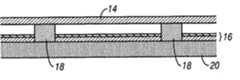
如下文将关于图8A到图10B描述的某些实施例涉及一种封装MEMS显示装置的方法及其所获得的装置。在一个实施例中,将背板接合到上面包含干涉式调制器阵列的衬底。所述衬底包含比可移动层高的柱。在组装时,背板与柱接触但不与可移动层接触。背板、衬底和柱一起保护干涉式调制器不受外力影响。在其它实施例中,不同的结构形成于衬底和背板上以保持背板与衬底之间的最小距离,且防止背板与可移动层接触。Certain embodiments as will be described below with respect to FIGS. 8A to 10B relate to a method of packaging a MEMS display device and the device obtained therefrom. In one embodiment, the backplate is bonded to the substrate on which the array of interferometric modulators is contained. The substrate includes posts that are taller than the movable layer. When assembled, the backplate is in contact with the posts but not with the movable layer. Together, the backplate, substrate, and posts protect the interferometric modulators from external forces. In other embodiments, different structures are formed on the substrate and backplate to maintain a minimum distance between the backplate and the substrate and prevent the backplate from contacting the movable layer.
图8A到图8B展示在封装中包括干涉式调制器阵列的显示器的实施例的侧视图。在此实施例中,将背板接合到上面包含干涉式调制器阵列的衬底。干涉式调制器阵列包含连接可移动层的柱。在组装后,背板即刻与柱接触但不与可移动层接触。背板、衬底和柱一起保护干涉式调制器不受外力影响。8A-8B show side views of an embodiment of a display including an array of interferometric modulators in a package. In this embodiment, the backplate is bonded to the substrate on which the array of interferometric modulators is contained. The interferometric modulator array consists of posts connecting movable layers. Immediately after assembly, the backplate is in contact with the posts but not with the movable layer. Together, the backplate, substrate, and posts protect the interferometric modulators from external forces.
如图所示,封装包括透明衬底20和背板62。背板62可为玻璃、金属、箔、聚合物、塑料和陶瓷或例如硅等半导体材料。透明衬底20可为能够使薄膜MEMS装置建置于其上的任何透明物质。实例包含玻璃、塑料和透明聚合物。As shown, the package includes a
在衬底20的背侧上形成干涉式调制器阵列。衬底的背侧是指衬底20的远离显示器的观看者的一侧。On the backside of
图8A到图8B中的阵列的所描绘部分包含两个邻近的干涉式调制器12a和12b。如所说明,每一干涉式调制器包含可移动反射层14,其定位于距光学堆叠16可变且可控的距离处,以形成具有至少一个可变尺寸的谐振光学间隙。可移动反射层14可如图7A到图7E中所说明以各种方式连接到支撑结构。举例来说,可移动反射层14可如图8A中所示在系链32上附接到支撑件18。The depicted portion of the array in Figures 8A-8B includes two adjacent
如本文所参考,光学堆叠16通常包括若干熔合层,所述熔合层可包含例如氧化铟锡(ITO)的电极层、例如铬的部分反射层以及透明电介质。因此,光学堆叠16是导电的、部分透明且部分反射的,且可(例如)通过将上述层中的一者或一者以上沉积到透明衬底20上来制造。As referred to herein,
如关于图1所描述,在一些实施例中,光学堆叠16可形成行电极。例如铝等高度导电且反射的材料可用于可移动反射层14,且可形成显示装置中的列电极。柱18连接到可移动反射层14的电极,且因此连接到显示装置的列电极。As described with respect to FIG. 1 , in some embodiments
将背板62接合到衬底20的背侧以形成封装。在一个实施例中,经由非气密密封件(未图示)将背板62接合到衬底20。背板62需要与衬底20分离至少预定最小距离,使得背板62不损坏像素12a和12b的结构或干扰其起作用。A
图8B说明其中背板62接合到衬底20的示范性显示器。如图所示,柱18中的至少一者在背板62接合到衬底20之后与背板62接触,因此使背板62与衬底20分离。对背板62的机械支撑因此来自用以连接可移动反射层16的至少一个柱18。在示范性实施例中,柱18比可移动反射层16高,使得背板62与柱18接触但不与可移动反射层16接触。FIG. 8B illustrates an exemplary display in which
在一个实施例中,柱18被设计成具有近似相同的高度。因此,近似所有的柱18均与背板62接触,因此对背板62提供机械支撑。在另一实施例中,柱18中的一些柱被设计成比其它的柱高。柱18中仅是所有柱中最高的部分与背板62接触。In one embodiment,
封装MEMS显示装置的示范性方法描述如下。提供透明衬底20。在衬底20的背侧上制造MEMS显示元件(例如干涉式调制器12a和12b)阵列。接着提供背板62。将背板62接合到衬底20的背侧。图8B中展示封装中的所得MEMS显示装置。An exemplary method of packaging a MEMS display device is described below. A
图9A到图9B展示在封装中包括干涉式调制器阵列的显示器的另一实施例。图9A到图9B展示所述实施例的侧视图。背板62包含支柱64。当接合到衬底20时,背板62与衬底20对准以使得每一支柱64与衬底20上的像素之间的合适的焊盘焊接区域66对准。在组装后,背板62即刻与支柱64接触但不与可移动层14接触。背板、衬底和支柱64一起保护干涉式调制器不受外力影响。9A-9B show another embodiment of a display including an array of interferometric modulators in a package. 9A-9B show side views of the embodiment.
图9B说明其中背板62接合到衬底20的示范性显示器。如图所示,支柱64与衬底20上的焊盘焊接区域66接触,因此使背板62与衬底20分离。柱18不与背板62接触且因此不承受来自背板62的机械力。FIG. 9B illustrates an exemplary display in which
在封装中,支柱64和对应的焊盘焊接区域66经选择以使得在组装后,支柱64即刻不干扰像素12a和12b的工作。支柱64通常被设计成具有相同高度。在一些实施例中,支柱64被设计成相同的以简化制造工艺。而且,支柱64被设计成具有适当高度以使得在组装后衬底20上的柱18即刻不与背板62接触。In the package, post 64 and corresponding
在一个实施例中,每一焊盘焊接区域66包含衬底20的表面中的一孔。当将背板62接合到衬底20时,每一支柱64与对应焊盘焊接区域66的孔对准且接着下落到所述孔中。In one embodiment, each
图10A到图10B展示在封装中包括干涉式调制器阵列的显示器的另一实施例的侧视图。在此实施例中,支柱64制造在衬底20上而不是如图9A到图9B的先前实施例中所示制造在背板62上。在组装后,背板即刻不与可移动层接触。背板和衬底一起保护干涉式调制器不受外力影响。10A-10B show side views of another embodiment of a display including an array of interferometric modulators in a package. In this embodiment, the
图10B说明其中背板62接合到衬底20的示范性显示器。如图所示,支柱64在背板62接合到衬底20之后与背板62接触,因此使背板62与衬底20分离。对背板62的机械支撑因此来自支柱64。柱18现在不与背板62接触,且因此不受来自背板62的机械力。FIG. 10B illustrates an exemplary display in which
支柱64位于像素12a与12b之间的合适区域中,使得支柱64不干扰像素12a和12b的起作用。支柱64通常被设计成具有相同高度。在一些实施例中,支柱64被设计成相同的以简化制造工艺。而且,支柱64被设计成具有适当高度,使得在组装后衬底20上的柱18即刻不与背板62接触。
在一个实施例(未说明)中,支柱位于背板和衬底两者上。支柱可具有相同高度,且衬底和背板中的每一者可具有经定位以接纳支柱的孔。In one embodiment (not illustrated), the posts are on both the backplate and the substrate. The posts can be of the same height, and each of the substrate and backplate can have holes positioned to receive the posts.
上述实施例涉及一种封装显示装置的方法及其所获得的显示装置。虽然使用干涉式调制器阵列作为实例来描述示范性实施例,但实施例不应限于干涉式调制器。这些实施例适用于任何合适的MEMS显示元件和其它类型的显示元件。The above-mentioned embodiments relate to a method of packaging a display device and the obtained display device. Although exemplary embodiments are described using an array of interferometric modulators as an example, the embodiments should not be limited to interferometric modulators. These embodiments are applicable to any suitable MEMS display element and other types of display elements.
以上描述内容详述了本发明的某些实施例。然而,将了解,不管以上内容在文字上看起来如何详细,均可以许多方式来实践本发明。应注意,当描述本发明的某些特征或方面时,特定术语的使用不应被理解为暗示所述术语在本文中被重新定义成局限于包含本发明的所述术语与之相关联的特征或方面的任何特定特性。The foregoing description details certain embodiments of the invention. It will be appreciated, however, that no matter how detailed the above may appear in text, the present invention can be practiced in many ways. It should be noted that when describing certain features or aspects of the invention, the use of a particular term should not be construed as implying that the term is redefined herein to be limited to encompassing the feature of the invention with which the term is associated. or any specific feature of the aspect.
Claims (41)
Applications Claiming Priority (3)
| Application Number | Priority Date | Filing Date | Title |
|---|---|---|---|
| US12/146,388 | 2008-06-25 | ||
| US12/146,388US7746539B2 (en) | 2008-06-25 | 2008-06-25 | Method for packing a display device and the device obtained thereof |
| PCT/US2009/048326WO2009158355A2 (en) | 2008-06-25 | 2009-06-23 | A method for packaging a display device and the device obtained thereof |
Publications (2)
| Publication Number | Publication Date |
|---|---|
| CN102076602A CN102076602A (en) | 2011-05-25 |
| CN102076602Btrue CN102076602B (en) | 2014-06-18 |
Family
ID=41445267
Family Applications (1)
| Application Number | Title | Priority Date | Filing Date |
|---|---|---|---|
| CN200980124408.7AExpired - Fee RelatedCN102076602B (en) | 2008-06-25 | 2009-06-23 | Method for encapsulating a display device and device obtained therefrom |
Country Status (6)
| Country | Link |
|---|---|
| US (1) | US7746539B2 (en) |
| EP (1) | EP2305011A2 (en) |
| JP (2) | JP5607618B2 (en) |
| KR (1) | KR20110020913A (en) |
| CN (1) | CN102076602B (en) |
| WO (1) | WO2009158355A2 (en) |
Families Citing this family (22)
| Publication number | Priority date | Publication date | Assignee | Title |
|---|---|---|---|---|
| US7527998B2 (en) | 2006-06-30 | 2009-05-05 | Qualcomm Mems Technologies, Inc. | Method of manufacturing MEMS devices providing air gap control |
| US8941631B2 (en) | 2007-11-16 | 2015-01-27 | Qualcomm Mems Technologies, Inc. | Simultaneous light collection and illumination on an active display |
| US7944604B2 (en) | 2008-03-07 | 2011-05-17 | Qualcomm Mems Technologies, Inc. | Interferometric modulator in transmission mode |
| US7859740B2 (en) | 2008-07-11 | 2010-12-28 | Qualcomm Mems Technologies, Inc. | Stiction mitigation with integrated mech micro-cantilevers through vertical stress gradient control |
| US7855826B2 (en)* | 2008-08-12 | 2010-12-21 | Qualcomm Mems Technologies, Inc. | Method and apparatus to reduce or eliminate stiction and image retention in interferometric modulator devices |
| US8358266B2 (en) | 2008-09-02 | 2013-01-22 | Qualcomm Mems Technologies, Inc. | Light turning device with prismatic light turning features |
| US8270056B2 (en) | 2009-03-23 | 2012-09-18 | Qualcomm Mems Technologies, Inc. | Display device with openings between sub-pixels and method of making same |
| CN102449512A (en) | 2009-05-29 | 2012-05-09 | 高通Mems科技公司 | Illumination devices and methods of fabrication thereof |
| US8270062B2 (en) | 2009-09-17 | 2012-09-18 | Qualcomm Mems Technologies, Inc. | Display device with at least one movable stop element |
| US8488228B2 (en) | 2009-09-28 | 2013-07-16 | Qualcomm Mems Technologies, Inc. | Interferometric display with interferometric reflector |
| KR20130100232A (en) | 2010-04-09 | 2013-09-10 | 퀄컴 엠이엠에스 테크놀로지스, 인크. | Mechanical layer of an electromechanical device and methods of forming the same |
| CN103109315A (en) | 2010-08-17 | 2013-05-15 | 高通Mems科技公司 | Actuation and calibration of a charge neutral electrode in an interferometric display device |
| US9057872B2 (en) | 2010-08-31 | 2015-06-16 | Qualcomm Mems Technologies, Inc. | Dielectric enhanced mirror for IMOD display |
| US8963159B2 (en) | 2011-04-04 | 2015-02-24 | Qualcomm Mems Technologies, Inc. | Pixel via and methods of forming the same |
| US9134527B2 (en) | 2011-04-04 | 2015-09-15 | Qualcomm Mems Technologies, Inc. | Pixel via and methods of forming the same |
| US8659816B2 (en) | 2011-04-25 | 2014-02-25 | Qualcomm Mems Technologies, Inc. | Mechanical layer and methods of making the same |
| JP5727303B2 (en)* | 2011-06-03 | 2015-06-03 | ピクストロニクス,インコーポレイテッド | Display device |
| US8742570B2 (en)* | 2011-09-09 | 2014-06-03 | Qualcomm Mems Technologies, Inc. | Backplate interconnect with integrated passives |
| US8736939B2 (en) | 2011-11-04 | 2014-05-27 | Qualcomm Mems Technologies, Inc. | Matching layer thin-films for an electromechanical systems reflective display device |
| US20140029078A1 (en)* | 2012-07-24 | 2014-01-30 | Qualcomm Mems Technologies, Inc. | Devices and methods for protecting electromechanical device arrays |
| JP6384239B2 (en) | 2014-09-29 | 2018-09-05 | セイコーエプソン株式会社 | Optical filter device, optical module, and electronic apparatus |
| JP6613564B2 (en) | 2014-12-26 | 2019-12-04 | セイコーエプソン株式会社 | Optical filter device, optical module, and electronic apparatus |
Citations (3)
| Publication number | Priority date | Publication date | Assignee | Title |
|---|---|---|---|---|
| CN1677686A (en)* | 2004-03-31 | 2005-10-05 | 富士通株式会社 | Microswitching device and method of manufacturing microswitching device |
| WO2006001918A2 (en)* | 2004-06-15 | 2006-01-05 | Reflectivity, Inc. | Micromirror array assembly with in-array pillars |
| WO2006020812A1 (en)* | 2004-08-10 | 2006-02-23 | Robertshaw Controls Company | System and method for verifying installation of a tank level monitor |
Family Cites Families (197)
| Publication number | Priority date | Publication date | Assignee | Title |
|---|---|---|---|---|
| US3728030A (en)* | 1970-06-22 | 1973-04-17 | Cary Instruments | Polarization interferometer |
| JPS4946974A (en)* | 1972-09-11 | 1974-05-07 | ||
| NL8001281A (en) | 1980-03-04 | 1981-10-01 | Philips Nv | DISPLAY DEVICE. |
| US4441791A (en)* | 1980-09-02 | 1984-04-10 | Texas Instruments Incorporated | Deformable mirror light modulator |
| US5096279A (en)* | 1984-08-31 | 1992-03-17 | Texas Instruments Incorporated | Spatial light modulator and method |
| US4859060A (en) | 1985-11-26 | 1989-08-22 | 501 Sharp Kabushiki Kaisha | Variable interferometric device and a process for the production of the same |
| US4786128A (en) | 1986-12-02 | 1988-11-22 | Quantum Diagnostics, Ltd. | Device for modulating and reflecting electromagnetic radiation employing electro-optic layer having a variable index of refraction |
| DE3776157D1 (en)* | 1987-06-04 | 1992-02-27 | Walter Lukosz | OPTICAL MODULATION AND MEASURING PROCESS. |
| US4956619A (en) | 1988-02-19 | 1990-09-11 | Texas Instruments Incorporated | Spatial light modulator |
| US5028939A (en) | 1988-08-23 | 1991-07-02 | Texas Instruments Incorporated | Spatial light modulator system |
| US4982184A (en)* | 1989-01-03 | 1991-01-01 | General Electric Company | Electrocrystallochromic display and element |
| US5022745A (en) | 1989-09-07 | 1991-06-11 | Massachusetts Institute Of Technology | Electrostatically deformable single crystal dielectrically coated mirror |
| US4954789A (en) | 1989-09-28 | 1990-09-04 | Texas Instruments Incorporated | Spatial light modulator |
| US5287215A (en) | 1991-07-17 | 1994-02-15 | Optron Systems, Inc. | Membrane light modulation systems |
| US5170283A (en) | 1991-07-24 | 1992-12-08 | Northrop Corporation | Silicon spatial light modulator |
| US5240818A (en) | 1991-07-31 | 1993-08-31 | Texas Instruments Incorporated | Method for manufacturing a color filter for deformable mirror device |
| US5315370A (en)* | 1991-10-23 | 1994-05-24 | Bulow Jeffrey A | Interferometric modulator for optical signal processing |
| TW245772B (en)* | 1992-05-19 | 1995-04-21 | Akzo Nv | |
| US5818095A (en) | 1992-08-11 | 1998-10-06 | Texas Instruments Incorporated | High-yield spatial light modulator with light blocking layer |
| FI96450C (en) | 1993-01-13 | 1996-06-25 | Vaisala Oy | Single-channel gas concentration measurement method and equipment |
| US7830587B2 (en)* | 1993-03-17 | 2010-11-09 | Qualcomm Mems Technologies, Inc. | Method and device for modulating light with semiconductor substrate |
| US6674562B1 (en)* | 1994-05-05 | 2004-01-06 | Iridigm Display Corporation | Interferometric modulation of radiation |
| US5559358A (en) | 1993-05-25 | 1996-09-24 | Honeywell Inc. | Opto-electro-mechanical device or filter, process for making, and sensors made therefrom |
| US5526172A (en) | 1993-07-27 | 1996-06-11 | Texas Instruments Incorporated | Microminiature, monolithic, variable electrical signal processor and apparatus including same |
| US5452024A (en)* | 1993-11-01 | 1995-09-19 | Texas Instruments Incorporated | DMD display system |
| FI94804C (en) | 1994-02-17 | 1995-10-25 | Vaisala Oy | Electrically adjustable surface micromechanical Fabry-Perot interferometer for optical material analysis |
| US5665997A (en) | 1994-03-31 | 1997-09-09 | Texas Instruments Incorporated | Grated landing area to eliminate sticking of micro-mechanical devices |
| US7123216B1 (en)* | 1994-05-05 | 2006-10-17 | Idc, Llc | Photonic MEMS and structures |
| US6710908B2 (en)* | 1994-05-05 | 2004-03-23 | Iridigm Display Corporation | Controlling micro-electro-mechanical cavities |
| US7460291B2 (en)* | 1994-05-05 | 2008-12-02 | Idc, Llc | Separable modulator |
| US7808694B2 (en) | 1994-05-05 | 2010-10-05 | Qualcomm Mems Technologies, Inc. | Method and device for modulating light |
| US6680792B2 (en) | 1994-05-05 | 2004-01-20 | Iridigm Display Corporation | Interferometric modulation of radiation |
| US7738157B2 (en)* | 1994-05-05 | 2010-06-15 | Qualcomm Mems Technologies, Inc. | System and method for a MEMS device |
| US20010003487A1 (en) | 1996-11-05 | 2001-06-14 | Mark W. Miles | Visible spectrum modulator arrays |
| US7550794B2 (en)* | 2002-09-20 | 2009-06-23 | Idc, Llc | Micromechanical systems device comprising a displaceable electrode and a charge-trapping layer |
| US7852545B2 (en)* | 1994-05-05 | 2010-12-14 | Qualcomm Mems Technologies, Inc. | Method and device for modulating light |
| US7826120B2 (en)* | 1994-05-05 | 2010-11-02 | Qualcomm Mems Technologies, Inc. | Method and device for multi-color interferometric modulation |
| US8081369B2 (en)* | 1994-05-05 | 2011-12-20 | Qualcomm Mems Technologies, Inc. | System and method for a MEMS device |
| US6040937A (en)* | 1994-05-05 | 2000-03-21 | Etalon, Inc. | Interferometric modulation |
| US5920418A (en) | 1994-06-21 | 1999-07-06 | Matsushita Electric Industrial Co., Ltd. | Diffractive optical modulator and method for producing the same, infrared sensor including such a diffractive optical modulator and method for producing the same, and display device including such a diffractive optical modulator |
| US5636052A (en) | 1994-07-29 | 1997-06-03 | Lucent Technologies Inc. | Direct view display based on a micromechanical modulation |
| US5485304A (en) | 1994-07-29 | 1996-01-16 | Texas Instruments, Inc. | Support posts for micro-mechanical devices |
| US5661592A (en) | 1995-06-07 | 1997-08-26 | Silicon Light Machines | Method of making and an apparatus for a flat diffraction grating light valve |
| US6046840A (en) | 1995-06-19 | 2000-04-04 | Reflectivity, Inc. | Double substrate reflective spatial light modulator with self-limiting micro-mechanical elements |
| US6324192B1 (en) | 1995-09-29 | 2001-11-27 | Coretek, Inc. | Electrically tunable fabry-perot structure utilizing a deformable multi-layer mirror and method of making the same |
| JPH09127551A (en)* | 1995-10-31 | 1997-05-16 | Sharp Corp | Semiconductor device and active matrix substrate |
| US5999306A (en) | 1995-12-01 | 1999-12-07 | Seiko Epson Corporation | Method of manufacturing spatial light modulator and electronic device employing it |
| US5825528A (en) | 1995-12-26 | 1998-10-20 | Lucent Technologies Inc. | Phase-mismatched fabry-perot cavity micromechanical modulator |
| US5751469A (en) | 1996-02-01 | 1998-05-12 | Lucent Technologies Inc. | Method and apparatus for an improved micromechanical modulator |
| US5710656A (en)* | 1996-07-30 | 1998-01-20 | Lucent Technologies Inc. | Micromechanical optical modulator having a reduced-mass composite membrane |
| US5838484A (en) | 1996-08-19 | 1998-11-17 | Lucent Technologies Inc. | Micromechanical optical modulator with linear operating characteristic |
| GB9619781D0 (en) | 1996-09-23 | 1996-11-06 | Secr Defence | Multi layer interference coatings |
| US6028689A (en)* | 1997-01-24 | 2000-02-22 | The United States Of America As Represented By The Secretary Of The Air Force | Multi-motion micromirror |
| US5786927A (en) | 1997-03-12 | 1998-07-28 | Lucent Technologies Inc. | Gas-damped micromechanical structure |
| US6384952B1 (en) | 1997-03-27 | 2002-05-07 | Mems Optical Inc. | Vertical comb drive actuated deformable mirror device and method |
| US5867302A (en)* | 1997-08-07 | 1999-02-02 | Sandia Corporation | Bistable microelectromechanical actuator |
| WO1999036824A1 (en) | 1998-01-20 | 1999-07-22 | Seiko Epson Corporation | Optical switching device and image display device |
| US5914804A (en) | 1998-01-28 | 1999-06-22 | Lucent Technologies Inc | Double-cavity micromechanical optical modulator with plural multilayer mirrors |
| US6262697B1 (en) | 1998-03-20 | 2001-07-17 | Eastman Kodak Company | Display having viewable and conductive images |
| US7532377B2 (en) | 1998-04-08 | 2009-05-12 | Idc, Llc | Movable micro-electromechanical device |
| WO1999052006A2 (en) | 1998-04-08 | 1999-10-14 | Etalon, Inc. | Interferometric modulation of radiation |
| JP3919954B2 (en) | 1998-10-16 | 2007-05-30 | 富士フイルム株式会社 | Array type light modulation element and flat display driving method |
| WO2003007049A1 (en) | 1999-10-05 | 2003-01-23 | Iridigm Display Corporation | Photonic mems and structures |
| US6307663B1 (en) | 2000-01-26 | 2001-10-23 | Eastman Kodak Company | Spatial light modulator with conformal grating device |
| JP2001221913A (en) | 2000-02-08 | 2001-08-17 | Yokogawa Electric Corp | Fabry-Perot filter and infrared gas analyzer |
| KR20010112456A (en) | 2000-02-24 | 2001-12-20 | 요트.게.아. 롤페즈 | Display device comprising a light guide |
| US6836366B1 (en) | 2000-03-03 | 2004-12-28 | Axsun Technologies, Inc. | Integrated tunable fabry-perot filter and method of making same |
| US6698295B1 (en)* | 2000-03-31 | 2004-03-02 | Shipley Company, L.L.C. | Microstructures comprising silicon nitride layer and thin conductive polysilicon layer |
| EP1720347B1 (en) | 2000-07-03 | 2010-06-23 | Sony Corporation | Optical multilayer structure, optical switching device, and image display |
| JP2002062490A (en) | 2000-08-14 | 2002-02-28 | Canon Inc | Interferometric modulator |
| US6466354B1 (en) | 2000-09-19 | 2002-10-15 | Silicon Light Machines | Method and apparatus for interferometric modulation of light |
| US6556338B2 (en)* | 2000-11-03 | 2003-04-29 | Intpax, Inc. | MEMS based variable optical attenuator (MBVOA) |
| US6433917B1 (en) | 2000-11-22 | 2002-08-13 | Ball Semiconductor, Inc. | Light modulation device and system |
| US6906847B2 (en) | 2000-12-07 | 2005-06-14 | Reflectivity, Inc | Spatial light modulators with light blocking/absorbing areas |
| US6614576B2 (en)* | 2000-12-15 | 2003-09-02 | Texas Instruments Incorporated | Surface micro-planarization for enhanced optical efficiency and pixel performance in SLM devices |
| DE10064616C2 (en)* | 2000-12-22 | 2003-02-06 | Ovd Kinegram Ag Zug | Decorative film and method for labeling the decorative film |
| JP2002221678A (en) | 2001-01-25 | 2002-08-09 | Seiko Epson Corp | Optical switching device, manufacturing method thereof, and image display device |
| US6912078B2 (en) | 2001-03-16 | 2005-06-28 | Corning Incorporated | Electrostatically actuated micro-electro-mechanical devices and method of manufacture |
| US6661561B2 (en) | 2001-03-26 | 2003-12-09 | Creo Inc. | High frequency deformable mirror device |
| US6657832B2 (en) | 2001-04-26 | 2003-12-02 | Texas Instruments Incorporated | Mechanically assisted restoring force support for micromachined membranes |
| JP3740444B2 (en) | 2001-07-11 | 2006-02-01 | キヤノン株式会社 | Optical deflector, optical equipment using the same, torsional oscillator |
| JP4032216B2 (en)* | 2001-07-12 | 2008-01-16 | ソニー株式会社 | OPTICAL MULTILAYER STRUCTURE, ITS MANUFACTURING METHOD, OPTICAL SWITCHING DEVICE, AND IMAGE DISPLAY DEVICE |
| US6632698B2 (en) | 2001-08-07 | 2003-10-14 | Hewlett-Packard Development Company, L.P. | Microelectromechanical device having a stiffened support beam, and methods of forming stiffened support beams in MEMS |
| US6661562B2 (en)* | 2001-08-17 | 2003-12-09 | Lucent Technologies Inc. | Optical modulator and method of manufacture thereof |
| GB2381834B (en)* | 2001-09-07 | 2004-08-25 | Avon Polymer Prod Ltd | Noise and vibration suppressors |
| US20030053078A1 (en)* | 2001-09-17 | 2003-03-20 | Mark Missey | Microelectromechanical tunable fabry-perot wavelength monitor with thermal actuators |
| US6791735B2 (en)* | 2002-01-09 | 2004-09-14 | The Regents Of The University Of California | Differentially-driven MEMS spatial light modulator |
| US6608268B1 (en) | 2002-02-05 | 2003-08-19 | Memtronics, A Division Of Cogent Solutions, Inc. | Proximity micro-electro-mechanical system |
| US6794119B2 (en) | 2002-02-12 | 2004-09-21 | Iridigm Display Corporation | Method for fabricating a structure for a microelectromechanical systems (MEMS) device |
| US6574033B1 (en) | 2002-02-27 | 2003-06-03 | Iridigm Display Corporation | Microelectromechanical systems device and method for fabricating same |
| US6972882B2 (en) | 2002-04-30 | 2005-12-06 | Hewlett-Packard Development Company, L.P. | Micro-mirror device with light angle amplification |
| US6954297B2 (en) | 2002-04-30 | 2005-10-11 | Hewlett-Packard Development Company, L.P. | Micro-mirror device including dielectrophoretic liquid |
| JP2003340795A (en) | 2002-05-20 | 2003-12-02 | Sony Corp | Electrostatic drive type mems element and manufacturing method therefor, optical mems element, optical modulator, glv device and laser display |
| JP3801099B2 (en)* | 2002-06-04 | 2006-07-26 | 株式会社デンソー | Tunable filter, manufacturing method thereof, and optical switching device using the same |
| US6813059B2 (en) | 2002-06-28 | 2004-11-02 | Silicon Light Machines, Inc. | Reduced formation of asperities in contact micro-structures |
| US6822798B2 (en)* | 2002-08-09 | 2004-11-23 | Optron Systems, Inc. | Tunable optical filter |
| US7085121B2 (en)* | 2002-10-21 | 2006-08-01 | Hrl Laboratories, Llc | Variable capacitance membrane actuator for wide band tuning of microstrip resonators and filters |
| FR2846318B1 (en)* | 2002-10-24 | 2005-01-07 | Commissariat Energie Atomique | INTEGRATED ELECTROMECHANICAL MICROSTRUCTURE HAVING MEANS FOR ADJUSTING THE PRESSURE IN A SEALED CAVITY AND A METHOD OF ADJUSTING THE PRESSURE |
| US7370185B2 (en)* | 2003-04-30 | 2008-05-06 | Hewlett-Packard Development Company, L.P. | Self-packaged optical interference display device having anti-stiction bumps, integral micro-lens, and reflection-absorbing layers |
| US6958846B2 (en) | 2002-11-26 | 2005-10-25 | Reflectivity, Inc | Spatial light modulators with light absorbing areas |
| US6844959B2 (en)* | 2002-11-26 | 2005-01-18 | Reflectivity, Inc | Spatial light modulators with light absorbing areas |
| TWI289708B (en)* | 2002-12-25 | 2007-11-11 | Qualcomm Mems Technologies Inc | Optical interference type color display |
| JP2004212638A (en) | 2002-12-27 | 2004-07-29 | Fuji Photo Film Co Ltd | Optical modulator and plane display element |
| JP2004212680A (en) | 2002-12-27 | 2004-07-29 | Fuji Photo Film Co Ltd | Optical modulator array and method of manufacturing same |
| TW594155B (en) | 2002-12-27 | 2004-06-21 | Prime View Int Corp Ltd | Optical interference type color display and optical interference modulator |
| JP2004219843A (en)* | 2003-01-16 | 2004-08-05 | Seiko Epson Corp | Optical modulator, display device and manufacturing method thereof |
| TW200413810A (en) | 2003-01-29 | 2004-08-01 | Prime View Int Co Ltd | Light interference display panel and its manufacturing method |
| TW557395B (en) | 2003-01-29 | 2003-10-11 | Yen Sun Technology Corp | Optical interference type reflection panel and the manufacturing method thereof |
| TW200417806A (en) | 2003-03-05 | 2004-09-16 | Prime View Int Corp Ltd | A structure of a light-incidence electrode of an optical interference display plate |
| TW567355B (en) | 2003-04-21 | 2003-12-21 | Prime View Int Co Ltd | An interference display cell and fabrication method thereof |
| TWI226504B (en)* | 2003-04-21 | 2005-01-11 | Prime View Int Co Ltd | A structure of an interference display cell |
| TWI224235B (en) | 2003-04-21 | 2004-11-21 | Prime View Int Co Ltd | A method for fabricating an interference display cell |
| US7072093B2 (en) | 2003-04-30 | 2006-07-04 | Hewlett-Packard Development Company, L.P. | Optical interference pixel display with charge control |
| US7447891B2 (en)* | 2003-04-30 | 2008-11-04 | Hewlett-Packard Development Company, L.P. | Light modulator with concentric control-electrode structure |
| US6940630B2 (en) | 2003-05-01 | 2005-09-06 | University Of Florida Research Foundation, Inc. | Vertical displacement device |
| TW591716B (en)* | 2003-05-26 | 2004-06-11 | Prime View Int Co Ltd | A structure of a structure release and manufacturing the same |
| TW570896B (en)* | 2003-05-26 | 2004-01-11 | Prime View Int Co Ltd | A method for fabricating an interference display cell |
| TWI223855B (en)* | 2003-06-09 | 2004-11-11 | Taiwan Semiconductor Mfg | Method for manufacturing reflective spatial light modulator mirror devices |
| US7221495B2 (en) | 2003-06-24 | 2007-05-22 | Idc Llc | Thin film precursor stack for MEMS manufacturing |
| JP3786106B2 (en)* | 2003-08-11 | 2006-06-14 | セイコーエプソン株式会社 | Wavelength tunable optical filter and manufacturing method thereof |
| TWI251712B (en)* | 2003-08-15 | 2006-03-21 | Prime View Int Corp Ltd | Interference display plate |
| TW200506479A (en)* | 2003-08-15 | 2005-02-16 | Prime View Int Co Ltd | Color changeable pixel for an interference display |
| TWI231865B (en)* | 2003-08-26 | 2005-05-01 | Prime View Int Co Ltd | An interference display cell and fabrication method thereof |
| TWI230801B (en) | 2003-08-29 | 2005-04-11 | Prime View Int Co Ltd | Reflective display unit using interferometric modulation and manufacturing method thereof |
| JP3979982B2 (en)* | 2003-08-29 | 2007-09-19 | シャープ株式会社 | Interferometric modulator and display device |
| TWI232333B (en)* | 2003-09-03 | 2005-05-11 | Prime View Int Co Ltd | Display unit using interferometric modulation and manufacturing method thereof |
| US6982820B2 (en)* | 2003-09-26 | 2006-01-03 | Prime View International Co., Ltd. | Color changeable pixel |
| US7027204B2 (en)* | 2003-09-26 | 2006-04-11 | Silicon Light Machines Corporation | High-density spatial light modulator |
| TW593126B (en)* | 2003-09-30 | 2004-06-21 | Prime View Int Co Ltd | A structure of a micro electro mechanical system and manufacturing the same |
| JP2005121906A (en) | 2003-10-16 | 2005-05-12 | Fuji Photo Film Co Ltd | Reflection type optical modulation array element and exposure device |
| US7198873B2 (en)* | 2003-11-18 | 2007-04-03 | Asml Netherlands B.V. | Lithographic processing optimization based on hypersampled correlations |
| TWI235345B (en) | 2004-01-20 | 2005-07-01 | Prime View Int Co Ltd | A structure of an optical interference display unit |
| JP2005235403A (en) | 2004-02-17 | 2005-09-02 | Hitachi Displays Ltd | Organic EL display device |
| TWI256941B (en)* | 2004-02-18 | 2006-06-21 | Qualcomm Mems Technologies Inc | A micro electro mechanical system display cell and method for fabricating thereof |
| US7119945B2 (en) | 2004-03-03 | 2006-10-10 | Idc, Llc | Altering temporal response of microelectromechanical elements |
| TW200530669A (en) | 2004-03-05 | 2005-09-16 | Prime View Int Co Ltd | Interference display plate and manufacturing method thereof |
| TWI261683B (en) | 2004-03-10 | 2006-09-11 | Qualcomm Mems Technologies Inc | Interference reflective element and repairing method thereof |
| JP4581453B2 (en) | 2004-03-29 | 2010-11-17 | ソニー株式会社 | MEMS element, optical MEMS element, diffractive optical MEMS element, and laser display |
| US7476327B2 (en) | 2004-05-04 | 2009-01-13 | Idc, Llc | Method of manufacture for microelectromechanical devices |
| US7164520B2 (en) | 2004-05-12 | 2007-01-16 | Idc, Llc | Packaging for an interferometric modulator |
| TWI233916B (en)* | 2004-07-09 | 2005-06-11 | Prime View Int Co Ltd | A structure of a micro electro mechanical system |
| TWI270722B (en)* | 2004-07-23 | 2007-01-11 | Au Optronics Corp | Dual-side display panel |
| EP2246726B1 (en)* | 2004-07-29 | 2013-04-03 | QUALCOMM MEMS Technologies, Inc. | System and method for micro-electromechanical operating of an interferometric modulator |
| KR100648310B1 (en)* | 2004-09-24 | 2006-11-23 | 삼성전자주식회사 | Color conversion device using the brightness information of the image and display device having the same |
| US7372613B2 (en) | 2004-09-27 | 2008-05-13 | Idc, Llc | Method and device for multistate interferometric light modulation |
| US7944599B2 (en)* | 2004-09-27 | 2011-05-17 | Qualcomm Mems Technologies, Inc. | Electromechanical device with optical function separated from mechanical and electrical function |
| US7327510B2 (en)* | 2004-09-27 | 2008-02-05 | Idc, Llc | Process for modifying offset voltage characteristics of an interferometric modulator |
| US7302157B2 (en) | 2004-09-27 | 2007-11-27 | Idc, Llc | System and method for multi-level brightness in interferometric modulation |
| US7564612B2 (en)* | 2004-09-27 | 2009-07-21 | Idc, Llc | Photonic MEMS and structures |
| US7321456B2 (en)* | 2004-09-27 | 2008-01-22 | Idc, Llc | Method and device for corner interferometric modulation |
| US7719500B2 (en)* | 2004-09-27 | 2010-05-18 | Qualcomm Mems Technologies, Inc. | Reflective display pixels arranged in non-rectangular arrays |
| US7130104B2 (en) | 2004-09-27 | 2006-10-31 | Idc, Llc | Methods and devices for inhibiting tilting of a mirror in an interferometric modulator |
| US7893919B2 (en)* | 2004-09-27 | 2011-02-22 | Qualcomm Mems Technologies, Inc. | Display region architectures |
| US7554714B2 (en)* | 2004-09-27 | 2009-06-30 | Idc, Llc | Device and method for manipulation of thermal response in a modulator |
| US7573547B2 (en)* | 2004-09-27 | 2009-08-11 | Idc, Llc | System and method for protecting micro-structure of display array using spacers in gap within display device |
| US7420725B2 (en) | 2004-09-27 | 2008-09-02 | Idc, Llc | Device having a conductive light absorbing mask and method for fabricating same |
| US7184202B2 (en)* | 2004-09-27 | 2007-02-27 | Idc, Llc | Method and system for packaging a MEMS device |
| US7289259B2 (en) | 2004-09-27 | 2007-10-30 | Idc, Llc | Conductive bus structure for interferometric modulator array |
| US7527995B2 (en)* | 2004-09-27 | 2009-05-05 | Qualcomm Mems Technologies, Inc. | Method of making prestructure for MEMS systems |
| US8102407B2 (en)* | 2004-09-27 | 2012-01-24 | Qualcomm Mems Technologies, Inc. | Method and device for manipulating color in a display |
| US7612932B2 (en)* | 2004-09-27 | 2009-11-03 | Idc, Llc | Microelectromechanical device with optical function separated from mechanical and electrical function |
| US7936497B2 (en)* | 2004-09-27 | 2011-05-03 | Qualcomm Mems Technologies, Inc. | MEMS device having deformable membrane characterized by mechanical persistence |
| US7630119B2 (en)* | 2004-09-27 | 2009-12-08 | Qualcomm Mems Technologies, Inc. | Apparatus and method for reducing slippage between structures in an interferometric modulator |
| US8008736B2 (en)* | 2004-09-27 | 2011-08-30 | Qualcomm Mems Technologies, Inc. | Analog interferometric modulator device |
| US7304784B2 (en)* | 2004-09-27 | 2007-12-04 | Idc, Llc | Reflective display device having viewable display on both sides |
| US20080068697A1 (en)* | 2004-10-29 | 2008-03-20 | Haluzak Charles C | Micro-Displays and Their Manufacture |
| US7675665B2 (en) | 2005-02-23 | 2010-03-09 | Pixtronix, Incorporated | Methods and apparatus for actuating displays |
| US8310442B2 (en)* | 2005-02-23 | 2012-11-13 | Pixtronix, Inc. | Circuits for controlling display apparatus |
| US7884989B2 (en) | 2005-05-27 | 2011-02-08 | Qualcomm Mems Technologies, Inc. | White interferometric modulators and methods for forming the same |
| US7460292B2 (en) | 2005-06-03 | 2008-12-02 | Qualcomm Mems Technologies, Inc. | Interferometric modulator with internal polarization and drive method |
| US7184195B2 (en)* | 2005-06-15 | 2007-02-27 | Miradia Inc. | Method and structure reducing parasitic influences of deflection devices in an integrated spatial light modulator |
| US8574823B2 (en)* | 2005-10-05 | 2013-11-05 | Hewlett-Packard Development Company, L.P. | Multi-level layer |
| US7916980B2 (en)* | 2006-01-13 | 2011-03-29 | Qualcomm Mems Technologies, Inc. | Interconnect structure for MEMS device |
| US7652814B2 (en) | 2006-01-27 | 2010-01-26 | Qualcomm Mems Technologies, Inc. | MEMS device with integrated optical element |
| US7550810B2 (en) | 2006-02-23 | 2009-06-23 | Qualcomm Mems Technologies, Inc. | MEMS device having a layer movable at asymmetric rates |
| US7649671B2 (en) | 2006-06-01 | 2010-01-19 | Qualcomm Mems Technologies, Inc. | Analog interferometric modulator device with electrostatic actuation and release |
| US7321457B2 (en)* | 2006-06-01 | 2008-01-22 | Qualcomm Incorporated | Process and structure for fabrication of MEMS device having isolated edge posts |
| US7835061B2 (en)* | 2006-06-28 | 2010-11-16 | Qualcomm Mems Technologies, Inc. | Support structures for free-standing electromechanical devices |
| US7385744B2 (en) | 2006-06-28 | 2008-06-10 | Qualcomm Mems Technologies, Inc. | Support structure for free-standing MEMS device and methods for forming the same |
| US7527998B2 (en) | 2006-06-30 | 2009-05-05 | Qualcomm Mems Technologies, Inc. | Method of manufacturing MEMS devices providing air gap control |
| US7629197B2 (en)* | 2006-10-18 | 2009-12-08 | Qualcomm Mems Technologies, Inc. | Spatial light modulator |
| US8115987B2 (en) | 2007-02-01 | 2012-02-14 | Qualcomm Mems Technologies, Inc. | Modulating the intensity of light from an interferometric reflector |
| US7742220B2 (en) | 2007-03-28 | 2010-06-22 | Qualcomm Mems Technologies, Inc. | Microelectromechanical device and method utilizing conducting layers separated by stops |
| US7643202B2 (en) | 2007-05-09 | 2010-01-05 | Qualcomm Mems Technologies, Inc. | Microelectromechanical system having a dielectric movable membrane and a mirror |
| US7715085B2 (en) | 2007-05-09 | 2010-05-11 | Qualcomm Mems Technologies, Inc. | Electromechanical system having a dielectric movable membrane and a mirror |
| US7643199B2 (en) | 2007-06-19 | 2010-01-05 | Qualcomm Mems Technologies, Inc. | High aperture-ratio top-reflective AM-iMod displays |
| US7782517B2 (en) | 2007-06-21 | 2010-08-24 | Qualcomm Mems Technologies, Inc. | Infrared and dual mode displays |
| US7630121B2 (en)* | 2007-07-02 | 2009-12-08 | Qualcomm Mems Technologies, Inc. | Electromechanical device with optical function separated from mechanical and electrical function |
| US7773286B2 (en)* | 2007-09-14 | 2010-08-10 | Qualcomm Mems Technologies, Inc. | Periodic dimple array |
| US7847999B2 (en)* | 2007-09-14 | 2010-12-07 | Qualcomm Mems Technologies, Inc. | Interferometric modulator display devices |
| EP2203765A1 (en)* | 2007-10-23 | 2010-07-07 | Qualcomm Mems Technologies, Inc. | Adjustably transmissive mems-based devices |
| US7715079B2 (en) | 2007-12-07 | 2010-05-11 | Qualcomm Mems Technologies, Inc. | MEMS devices requiring no mechanical support |
| US8164821B2 (en) | 2008-02-22 | 2012-04-24 | Qualcomm Mems Technologies, Inc. | Microelectromechanical device with thermal expansion balancing layer or stiffening layer |
| US7944604B2 (en) | 2008-03-07 | 2011-05-17 | Qualcomm Mems Technologies, Inc. | Interferometric modulator in transmission mode |
| US7612933B2 (en) | 2008-03-27 | 2009-11-03 | Qualcomm Mems Technologies, Inc. | Microelectromechanical device with spacing layer |
| US7898723B2 (en) | 2008-04-02 | 2011-03-01 | Qualcomm Mems Technologies, Inc. | Microelectromechanical systems display element with photovoltaic structure |
| US7969638B2 (en) | 2008-04-10 | 2011-06-28 | Qualcomm Mems Technologies, Inc. | Device having thin black mask and method of fabricating the same |
- 2008
- 2008-06-25USUS12/146,388patent/US7746539B2/ennot_activeExpired - Fee Related
- 2009
- 2009-06-23EPEP09770889Apatent/EP2305011A2/ennot_activeWithdrawn
- 2009-06-23WOPCT/US2009/048326patent/WO2009158355A2/enactiveSearch and Examination
- 2009-06-23JPJP2011516544Apatent/JP5607618B2/ennot_activeExpired - Fee Related
- 2009-06-23CNCN200980124408.7Apatent/CN102076602B/ennot_activeExpired - Fee Related
- 2009-06-23KRKR1020117000942Apatent/KR20110020913A/ennot_activeAbandoned
- 2014
- 2014-06-18JPJP2014125364Apatent/JP2014170245A/enactivePending
Patent Citations (3)
| Publication number | Priority date | Publication date | Assignee | Title |
|---|---|---|---|---|
| CN1677686A (en)* | 2004-03-31 | 2005-10-05 | 富士通株式会社 | Microswitching device and method of manufacturing microswitching device |
| WO2006001918A2 (en)* | 2004-06-15 | 2006-01-05 | Reflectivity, Inc. | Micromirror array assembly with in-array pillars |
| WO2006020812A1 (en)* | 2004-08-10 | 2006-02-23 | Robertshaw Controls Company | System and method for verifying installation of a tank level monitor |
Also Published As
| Publication number | Publication date |
|---|---|
| US20090323165A1 (en) | 2009-12-31 |
| EP2305011A2 (en) | 2011-04-06 |
| JP2014170245A (en) | 2014-09-18 |
| WO2009158355A2 (en) | 2009-12-30 |
| JP2011526376A (en) | 2011-10-06 |
| JP5607618B2 (en) | 2014-10-15 |
| CN102076602A (en) | 2011-05-25 |
| WO2009158355A3 (en) | 2010-12-02 |
| US7746539B2 (en) | 2010-06-29 |
| KR20110020913A (en) | 2011-03-03 |
Similar Documents
| Publication | Publication Date | Title |
|---|---|---|
| CN102076602B (en) | Method for encapsulating a display device and device obtained therefrom | |
| US7724993B2 (en) | MEMS switches with deforming membranes | |
| US8023167B2 (en) | Backlight displays | |
| US7916378B2 (en) | Method and apparatus for providing a light absorbing mask in an interferometric modulator display | |
| US7304784B2 (en) | Reflective display device having viewable display on both sides | |
| US7345805B2 (en) | Interferometric modulator array with integrated MEMS electrical switches | |
| US7768690B2 (en) | Backlight displays | |
| US7916980B2 (en) | Interconnect structure for MEMS device | |
| US20080158648A1 (en) | Peripheral switches for MEMS display test | |
| CN101385066B (en) | Method and system for writing data to mems display elements | |
| JP4399404B2 (en) | Method and apparatus for a display with integrated transparent components | |
| US8022896B2 (en) | ESD protection for MEMS display panels | |
| US8115989B2 (en) | Anti-stiction electrode | |
| US7791783B2 (en) | Backlight displays | |
| EP1809568A2 (en) | Mems switches with deforming membranes | |
| JP5123198B2 (en) | MEMS switch with set and latch electrodes | |
| CN100547453C (en) | Reflective display device with viewable displays on both sides | |
| US7550912B2 (en) | Method and system for maintaining partial vacuum in display device | |
| JP2013511073A (en) | System and method for manufacturing a display device having an electrically connected front plate and back plate | |
| JP2013033260A (en) | Mems switch with set and latch electrodes |
Legal Events
| Date | Code | Title | Description |
|---|---|---|---|
| C06 | Publication | ||
| PB01 | Publication | ||
| C10 | Entry into substantive examination | ||
| SE01 | Entry into force of request for substantive examination | ||
| C14 | Grant of patent or utility model | ||
| GR01 | Patent grant | ||
| C41 | Transfer of patent application or patent right or utility model | ||
| TR01 | Transfer of patent right | Effective date of registration:20161026 Address after:American California Patentee after:NUJIRA LTD. Address before:American California Patentee before:Qualcomm MEMS Technology Corp. | |
| CF01 | Termination of patent right due to non-payment of annual fee | ||
| CF01 | Termination of patent right due to non-payment of annual fee | Granted publication date:20140618 Termination date:20190623 |