CN102074785A - RFID tag antenna with double-ended open-circuit coupling structure and its design method - Google Patents
RFID tag antenna with double-ended open-circuit coupling structure and its design methodDownload PDFInfo
- Publication number
- CN102074785A CN102074785ACN2009102226247ACN200910222624ACN102074785ACN 102074785 ACN102074785 ACN 102074785ACN 2009102226247 ACN2009102226247 ACN 2009102226247ACN 200910222624 ACN200910222624 ACN 200910222624ACN 102074785 ACN102074785 ACN 102074785A
- Authority
- CN
- China
- Prior art keywords
- antenna
- double
- coupler
- rfid tag
- coupling structure
- Prior art date
- Legal status (The legal status is an assumption and is not a legal conclusion. Google has not performed a legal analysis and makes no representation as to the accuracy of the status listed.)
- Pending
Links
- 238000010168coupling processMethods0.000titleclaimsabstractdescription26
- 238000005859coupling reactionMethods0.000titleclaimsabstractdescription26
- 230000008878couplingEffects0.000titleclaimsabstractdescription25
- 238000000034methodMethods0.000titleclaimsabstractdescription10
- 238000013461designMethods0.000titleabstractdescription5
- 230000000191radiation effectEffects0.000claimsdescription3
- 230000005855radiationEffects0.000abstractdescription8
- 238000010586diagramMethods0.000description8
- 239000000758substrateSubstances0.000description6
- 238000005516engineering processMethods0.000description5
- 230000000694effectsEffects0.000description2
- 230000001939inductive effectEffects0.000description2
- 238000004891communicationMethods0.000description1
- 230000009977dual effectEffects0.000description1
- 238000012986modificationMethods0.000description1
- 230000004048modificationEffects0.000description1
- 230000003287optical effectEffects0.000description1
- 230000001151other effectEffects0.000description1
- 238000012552reviewMethods0.000description1
Images


Landscapes
- Details Of Aerials (AREA)
Abstract
Description
Translated fromChinese技术领域technical field
本发明涉及一种射频辨识(RFID)标签天线,尤其是有关于一种具有双端开路耦合结构的宽频射频辨识标签天线。The invention relates to a radio frequency identification (RFID) tag antenna, in particular to a broadband radio frequency identification tag antenna with a double-ended open-circuit coupling structure.
背景技术Background technique
无线射频识别是一种通信技术,可通过无线电讯号识别特定目标并读写相关数据,而无需识别系统与特定目标之间建立机械或光学接触。随着无线射频识别技术的普及,许多手持式电子装置均内建有无线射频识别天线。Radio Frequency Identification is a communication technology that can identify a specific target and read and write related data through radio signals without the need for mechanical or optical contact between the identification system and the specific target. With the popularization of radio frequency identification technology, many handheld electronic devices have built-in radio frequency identification antennas.
无线射频识别天线依工作频率可分为低频天线、高频(high frequency,HF)天线、超高频(ultra high frequency,UHF)天线以及微波(microwave)天线。低频天线的工作频率是125KHz至134KHz,高频天线的工作频率是13.56MHz,超高频天线的工作频率是介于840MHz至960MHz之间,而微波天线的工作频率是2.45GHz至5.8GHz。一般而言,内建于手持式电子装置中的无线射频识别天线为超高频天线而超高频无线射频识别天线是通过辐射(radiation)的方式进行传输。Radio frequency identification antennas can be divided into low frequency antennas, high frequency (high frequency, HF) antennas, ultra high frequency (ultra high frequency, UHF) antennas and microwave (microwave) antennas according to their operating frequency. The operating frequency of the low-frequency antenna is 125KHz to 134KHz, the operating frequency of the high-frequency antenna is 13.56MHz, the operating frequency of the UHF antenna is between 840MHz and 960MHz, and the operating frequency of the microwave antenna is 2.45GHz to 5.8GHz. Generally speaking, the RFID antenna built in the handheld electronic device is a UHF antenna, and the UHF RFID antenna transmits through radiation.
美国公告号7545928案揭示一种射频辨识标签10及其阻抗匹配方法,如图1,其具有一天线本体101及一耦合回圈102其置于一基板103上并具有两馈入点102a/102b。所述耦合回圈102因阻抗匹配的缘故,其本身是一个小型电感,几乎不具有辐射功能,也就是说,为顾及天线与芯片之间的阻抗匹配,需使用几乎无辐射功能的小型耦合回圈102(所述小型耦合回圈102通常小于天线本体101的30%)使天线的输入阻抗带有足够的感抗(inductive reactance),以消除芯片所带有的容抗(capacitive reactance),从而达成共轭匹配,如果达成匹配其输入口(input port)反射损失(return loss)将如图1a所示,其阻抗特性如图2所示(其中天线的输入阻抗的实部以Ra表示,虚部以Xa表示;芯片的输入阻抗的实部以Rc表示,虚部以Xc表示)。US Publication No. 7545928 discloses a radio
因此,本案的发明人是研究出一种新的射频辨识标签天线,尤其是有关于一种具有双端开路耦合结构的射频辨识标签天线,是可达成与先前技术相同(或较佳)频宽表现。Therefore, the inventor of this case is to develop a new radio frequency identification tag antenna, especially about a radio frequency identification tag antenna with a double-ended open-circuit coupling structure, which can achieve the same (or better) bandwidth than the prior art Performance.
发明内容Contents of the invention
本发明的目的在于提供一种具有双端开路耦合结构的射频辨识标签天线及其设计方法,其是一种新的UHF频段的射频辨识标签天线,是可增加频宽并提升辐射效能。The purpose of the present invention is to provide a radio frequency identification tag antenna with a double-ended open-circuit coupling structure and a design method thereof, which is a new UHF frequency band radio frequency identification tag antenna, which can increase the bandwidth and improve the radiation efficiency.
本发明是关于一种双端开路耦合结构的射频辨识标签天线,其至少包含:The present invention relates to a radio frequency identification tag antenna with a double-ended open-circuit coupling structure, which at least includes:
一天线本体(anntena body),其长度约为1/2波长,是可决定一谐振(resonance)频率;以及一耦合器,是可使天线本体所接收的射频信号耦合至芯片中;其中,所述耦合器为双端开路的线型结构,其长度约略为1/2波长,亦可被视为一个具有辐射效能的偶极天线。An antenna body (anntena body), whose length is about 1/2 wavelength, can determine a resonance (resonance) frequency; and a coupler, can couple the radio frequency signal received by the antenna body to the chip; wherein, the The aforementioned coupler is a double-ended open-circuit linear structure, and its length is about 1/2 wavelength, which can also be regarded as a dipole antenna with radiation performance.
本发明是关于一种应用于一射频辨识标签的设计方法,包含以下三步骤:The present invention relates to a design method applied to a radio frequency identification tag, which includes the following three steps:
1.所述天线的中心工作频率可通过调整天线本体的长度而决定。1. The central operating frequency of the antenna can be determined by adjusting the length of the antenna body.
2.所述天线的实部阻抗可通过调整天线本体与耦合器之间的距离,使其与芯片的实部阻抗达成匹配。2. The real part impedance of the antenna can be matched with the real part impedance of the chip by adjusting the distance between the antenna body and the coupler.
3.所述天线的虚部阻抗可通过调整耦合器的长度,使其与芯片的虚部阻抗达成共轭匹配。3. The imaginary impedance of the antenna can be conjugate-matched with the imaginary impedance of the chip by adjusting the length of the coupler.
为使贵审查委员对于本发明的结构目的和功效有更进一步的了解与认同,现配合图示范例详细说明如后。In order to make your review committee members have a further understanding and recognition of the structure, purpose and efficacy of the present invention, the detailed description is as follows with the illustrations and examples.
附图说明Description of drawings
图1为先前技术射频辨识标签的示意图;FIG. 1 is a schematic diagram of a prior art radio frequency identification tag;
图1a为先前技术射频辨识标签天线的工作频宽示意图;FIG. 1a is a schematic diagram of the working bandwidth of the radio frequency identification tag antenna in the prior art;
图2为先前技术射频辨识标签天线与芯片的阻抗匹配示意图;FIG. 2 is a schematic diagram of impedance matching between an antenna of a radio frequency identification tag and a chip in the prior art;
图3为用于本发明射频辨识标签一较佳实施例示意图;Fig. 3 is a schematic diagram of a preferred embodiment for the radio frequency identification tag of the present invention;
图3a为用于本发明射频辨识标签另一较佳实施例示意图;Figure 3a is a schematic diagram of another preferred embodiment of the radio frequency identification tag of the present invention;
图4为本发明的虚部阻抗图;Fig. 4 is the imaginary part impedance figure of the present invention;
图5为本发明的实部阻抗图;Fig. 5 is the real part impedance figure of the present invention;
图6为本发明的反射损失(return loss)的信号图;Fig. 6 is the signal figure of reflection loss (return loss) of the present invention;
图6a为用于本发明射频辨识标签另一较佳实施例示意图;Fig. 6a is a schematic diagram of another preferred embodiment of the radio frequency identification tag of the present invention;
图6b为用于本发明射频辨识标签另一较佳实施例示意图;以及Figure 6b is a schematic diagram of another preferred embodiment of the RFID tag used in the present invention; and
图7为本发明以贴片天线(patch antenna)的型式实施的范例。FIG. 7 shows an example of the invention implemented in the form of a patch antenna.
附图标记说明:10-射频辨识标签;101-天线本体;102-耦合回圈;103-基板;301-天线本体;302-双端开路耦合器;303-基板;304-射频辨识芯片;602-耦合器;603-天线本体;604-耦合器;605/606-双天线本体;701-芯片;702-耦合器;703-天线本体;704-接地基板。Description of reference signs: 10-radio frequency identification label; 101-antenna body; 102-coupling loop; 103-substrate; 301-antenna body; 302-double-ended open-circuit coupler; 303-substrate; 304-radio frequency identification chip; -coupler; 603-antenna body; 604-coupler; 605/606-double antenna body; 701-chip; 702-coupler; 703-antenna body; 704-ground substrate.
具体实施方式Detailed ways
有关本发明为达成上述目的,所采用的技术、手段及其他的功效,现举一较佳可行实施例并配合图式详细说明如后,相信本发明上述的目的、特征及其他的优点,当可由的得一深入而具体的了解,但本发明并非惟一的实施例,容此说明之。For the present invention to achieve the above-mentioned purpose, the technology, means and other effects adopted, now give a preferred feasible embodiment and cooperate with the drawings in detail as follows, believe that the above-mentioned purpose of the present invention, features and other advantages, when An in-depth and specific understanding can be obtained from the above, but the present invention is not the only embodiment, so please describe it here.
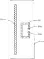
图3为本发明的一较佳实施例,其亦具有一天线本体301及一双端开路耦合器302其可被置于一基板303上。天线本体301及双端开路耦合器302可以是一个偶极(dipole)天线,但不限于偶极天线,此双端开路耦合器302的RFID标签天线,其输入口302a/302b(input port)乃是置于耦合器302上,通常在耦合器302开路两端的中央,但也不限于中央。FIG. 3 is a preferred embodiment of the present invention, which also has an antenna body 301 and a double-ended open-circuit coupler 302 which can be placed on a substrate 303 . Antenna body 301 and double-ended open circuit coupler 302 can be a dipole (dipole) antenna, but not limited to dipole antenna, the RFID tag antenna of this double-ended open circuit coupler 302, its input port 302a/302b (input port) is It is placed on the coupler 302, usually in the center of the two open ends of the coupler 302, but not limited to the center.
图3较佳实施例所述射频辨识标签,其进一步包含一射频辨识芯片304,所述射频辨识芯片304经由所述耦合器302上的输入口的一极302a以及输入口的另一极302b接收或输入一射频信号。The radio frequency identification tag of the preferred embodiment of Fig. 3 further includes a radio frequency identification chip 304, and the radio frequency identification chip 304 receives a pole 302a of the input port on the coupler 302 and another pole 302b of the input port. Or input a radio frequency signal.
此时耦合器302可设计为围绕天线本体301,可以围绕天线本体的外缘,也可以围绕天线本体的内缘,如图3a所示。所述天线可以工作在UHF频段及微波频段。At this time, the coupler 302 can be designed to surround the antenna body 301 , either around the outer edge of the antenna body, or around the inner edge of the antenna body, as shown in FIG. 3 a . The antenna can work in UHF frequency band and microwave frequency band.
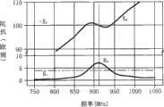
现由图3进一步说明,为使天线的输入阻抗达成电感性时,耦合器302的总长度通常约略大于1/2波长。反之,为使天线的输入阻抗达成电容性时,耦合器302的总长度通常约略小于1/2波长。相对于先前技术的阻抗匹配调整方法,本发明所采用的方法,在达成阻抗匹配的同时,亦通过耦合器302本身的辐射效能,进而提高天线整体的辐射效能。所述天线输入阻抗的电抗值(reactance)随着耦合器长度的变化而有所改变,其关系如图4所示。It is further illustrated by FIG. 3 that, in order to make the input impedance of the antenna inductive, the total length of the coupler 302 is usually slightly longer than 1/2 wavelength. On the contrary, to make the input impedance of the antenna capacitive, the total length of the coupler 302 is usually slightly less than 1/2 wavelength. Compared with the impedance matching adjustment method of the prior art, the method adopted in the present invention not only achieves impedance matching, but also improves the overall radiation performance of the antenna through the radiation performance of the coupler 302 itself. The reactance of the input impedance of the antenna changes with the length of the coupler, and the relationship is shown in FIG. 4 .
现由图5再进一步说明,为使天线所需阻抗的实部可达到所需电阻值(resistance),耦合器302与天线本体301之间的距离d越近,电阻值也就越小;距离d越远,电阻值也就越大以达到所需阻抗的实部,其关系如图5所示。Now further illustrate by Fig. 5, in order to make the real part of the required impedance of the antenna reach the required resistance value (resistance), the closer the distance d between the coupler 302 and the antenna body 301, the smaller the resistance value; The farther d is, the larger the resistance value is to achieve the real part of the required impedance. The relationship is shown in Figure 5.
而本案相异于现有技术,乃是采用双端开路耦合器302取代耦合回圈102,而双端开路耦合器302本身就是一个偶极天线,其辐射效果强于所述的小型耦合回圈102,因此本发明所要求保护的具有双端开路耦合结构的射频辨识标签天线,其辐射效果及频宽表现将不亚于甚而优于前述技术。And this case is different from the prior art, but adopts double-ended open-circuit coupler 302 to replace
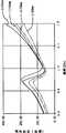
图6本发明的反射损失(return loss)的信号图,本发明可在阻抗匹配的情况下,达到以中心工作频率为准的30%的频宽。FIG. 6 is a signal diagram of the return loss of the present invention. The present invention can achieve a bandwidth of 30% based on the central operating frequency under the condition of impedance matching.
图4~图6的工作频率在此以超高频为例说明,但亦可由调整第一天线本体的长度以应用于微波电路使本体工作频率是2.45GHz至5.8GHz。其耦合器尺寸亦可随的变化在此不再赘述。The operating frequency of FIGS. 4-6 is described here as an example of ultra-high frequency, but the length of the first antenna body can also be adjusted to apply to microwave circuits so that the operating frequency of the first antenna body is 2.45 GHz to 5.8 GHz. The size of the coupler can also be changed accordingly and will not be repeated here.
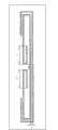
本发明的另一种实施方式,如图6a所示,其中天线本体603与耦合器602之间的平行距离可以保持固定,然而耦合器602的两端与天线本体603的两端,其距离d是可以改变的,改变此距离的效果与前述图3所示的实施例改变天线本体301与耦合器302之间的平行距离效果相同。Another embodiment of the present invention, as shown in Figure 6a, wherein the parallel distance between the
本发明亦可采用双天线本体的方式实施的,如图6b所示,其中双天线本体605/606与耦合器604之间的平行距离可以保持固定,然而耦合器604的四个端点与双天线本体605/606的四个端点,其距离d是可以改变的。改变此距离的效果与前述图3及图6所示的实施例的效果相同,其中双天线本体605/606的长度可以不必完全相等,此举可以造成双重耦合,进而增加工作频宽。上述具有双端开路耦合器302的RFID标签天线,也可以采用具有背面接地基板(ground plane)的微带天线(micro-strip antenna)的型式实施的;同理,上述具有双端开路耦合器302的RFID标签天线,也可以采用具有背面接地基板704(ground plane)的贴片天线703(patch antenna)的型式实施的,如以贴片天线703的型式实施的,则天线本体703可以是一个贴片天线,而其耦合器702可以是一个包含芯片701的双端开路的微带天线,如图7所示。The present invention can also be implemented in the form of a dual-antenna body, as shown in Figure 6b, wherein the parallel distance between the dual-antenna body 605/606 and the coupler 604 can be kept fixed, but the four terminals of the coupler 604 and the dual-antenna The distance d between the four endpoints of the body 605/606 can be changed. The effect of changing this distance is the same as that of the above-mentioned embodiments shown in FIG. 3 and FIG. 6 , where the lengths of the dual antenna bodies 605 and 606 do not have to be completely equal, which can cause double coupling and further increase the working bandwidth. The above-mentioned RFID tag antenna with double-ended open-circuit coupler 302 can also be implemented in the form of a micro-strip antenna (micro-strip antenna) with a backside ground plane; The RFID tag antenna can also be implemented in the form of a patch antenna 703 (patch antenna) with a back ground substrate 704 (ground plane). If implemented in the form of a
图3、图3a、以及图6a/b中所示的“L”是指耦合器两端其长度可以被调整以达到与耦合器上的芯片虚部阻抗匹配的参数,熟悉本项技术者可自行变化而不背离本发明的范围。"L" shown in Figure 3, Figure 3a, and Figure 6a/b refers to the parameter whose length at both ends of the coupler can be adjusted to match the impedance of the imaginary part of the chip on the coupler. Those familiar with this technology can changes without departing from the scope of the invention.
本发明亦提供一种应用于一射频辨识标签的设计方法,包含以下三步骤:The present invention also provides a design method applied to a radio frequency identification tag, which includes the following three steps:
1.提供一天线本体及一双端开路的耦合器以构成一天线;其中所述天线的中心工作频率是由所述天线本体的长度所决定。1. An antenna body and a double-ended open-circuit coupler are provided to form an antenna; wherein the central operating frequency of the antenna is determined by the length of the antenna body.
2.所述天线的实部阻抗是通过调整天线本体与耦合器之间的距离,使其与一芯片的实部阻抗达成匹配。2. The real part impedance of the antenna is matched with the real part impedance of a chip by adjusting the distance between the antenna body and the coupler.
3.所述天线的虚部阻抗是通过调整耦合器双端开路的长度,使其与所述芯片的虚部阻抗达成匹配。3. The imaginary part impedance of the antenna is matched with the imaginary part impedance of the chip by adjusting the length of the double-ended open circuit of the coupler.
以上说明对本发明而言只是说明性的,而非限制性的,本领域普通技术人员理解,在不脱离以下所附权利要求所限定的精神和范围的情况下,可做出许多修改,变化,或等效,但都将落入本发明的保护范围内。The above description is only illustrative, rather than restrictive, to the present invention. Those of ordinary skill in the art understand that many modifications and changes can be made without departing from the spirit and scope defined by the following appended claims. Or equivalent, but all will fall within the protection scope of the present invention.
Claims (12)
Translated fromChinesePriority Applications (1)
| Application Number | Priority Date | Filing Date | Title |
|---|---|---|---|
| CN2009102226247ACN102074785A (en) | 2009-11-19 | 2009-11-19 | RFID tag antenna with double-ended open-circuit coupling structure and its design method |
Applications Claiming Priority (1)
| Application Number | Priority Date | Filing Date | Title |
|---|---|---|---|
| CN2009102226247ACN102074785A (en) | 2009-11-19 | 2009-11-19 | RFID tag antenna with double-ended open-circuit coupling structure and its design method |
Publications (1)
| Publication Number | Publication Date |
|---|---|
| CN102074785Atrue CN102074785A (en) | 2011-05-25 |
Family
ID=44033201
Family Applications (1)
| Application Number | Title | Priority Date | Filing Date |
|---|---|---|---|
| CN2009102226247APendingCN102074785A (en) | 2009-11-19 | 2009-11-19 | RFID tag antenna with double-ended open-circuit coupling structure and its design method |
Country Status (1)
| Country | Link |
|---|---|
| CN (1) | CN102074785A (en) |
Cited By (4)
| Publication number | Priority date | Publication date | Assignee | Title |
|---|---|---|---|---|
| CN103473427A (en)* | 2013-09-24 | 2013-12-25 | 上海无线电设备研究所 | Complex impedance matching method applied to tag antenna design |
| CN105490013A (en)* | 2015-12-31 | 2016-04-13 | 上海炘璞电子科技有限公司 | Radio frequency identification antenna |
| CN105809079A (en)* | 2016-03-07 | 2016-07-27 | 广东华大互联网股份有限公司 | Dual-band operation method and dual-band radio frequency reader-writer |
| CN108539375A (en)* | 2018-03-30 | 2018-09-14 | 东华大学 | A kind of fabric base super high frequency radio frequency identification antenna and manufacturing method |
Citations (2)
| Publication number | Priority date | Publication date | Assignee | Title |
|---|---|---|---|---|
| US6259408B1 (en)* | 1999-11-19 | 2001-07-10 | Intermec Ip Corp. | RFID transponders with paste antennas and flip-chip attachment |
| CN101159035A (en)* | 2006-08-09 | 2008-04-09 | 富士通株式会社 | RFID tag and manufacturing method thereof |
- 2009
- 2009-11-19CNCN2009102226247Apatent/CN102074785A/enactivePending
Patent Citations (2)
| Publication number | Priority date | Publication date | Assignee | Title |
|---|---|---|---|---|
| US6259408B1 (en)* | 1999-11-19 | 2001-07-10 | Intermec Ip Corp. | RFID transponders with paste antennas and flip-chip attachment |
| CN101159035A (en)* | 2006-08-09 | 2008-04-09 | 富士通株式会社 | RFID tag and manufacturing method thereof |
Cited By (4)
| Publication number | Priority date | Publication date | Assignee | Title |
|---|---|---|---|---|
| CN103473427A (en)* | 2013-09-24 | 2013-12-25 | 上海无线电设备研究所 | Complex impedance matching method applied to tag antenna design |
| CN105490013A (en)* | 2015-12-31 | 2016-04-13 | 上海炘璞电子科技有限公司 | Radio frequency identification antenna |
| CN105809079A (en)* | 2016-03-07 | 2016-07-27 | 广东华大互联网股份有限公司 | Dual-band operation method and dual-band radio frequency reader-writer |
| CN108539375A (en)* | 2018-03-30 | 2018-09-14 | 东华大学 | A kind of fabric base super high frequency radio frequency identification antenna and manufacturing method |
Similar Documents
| Publication | Publication Date | Title |
|---|---|---|
| US7505001B2 (en) | Virtual short circuit for providing reference signal in RFID tag | |
| CN101593866B (en) | Dielectric resonance UHF RFID label antenna provided with T-shaped matching network | |
| EP2845264A1 (en) | Discontinuous loop antennas suitable for radio-frequency identification (rfid) tags, and related components, systems, and methods | |
| CN102496776B (en) | Tag antenna capable of covering global UHF RFID frequency ranges, electronic tag | |
| CN103107416B (en) | Radio frequency identification tag antenna | |
| CN101789543B (en) | Multi-system and multi-band frequency RFID (Radio Frequency Identification) antenna | |
| CN101355195A (en) | UHF RFID Dual Band Anti-Metal Tag Antenna | |
| CN104241824B (en) | A kind of universal combined reader antenna | |
| CN103531889B (en) | Small-sized broadband end-on-fire antenna | |
| EP2323075A1 (en) | RFID tag antenna using double-open ends coupler structure | |
| CN201303048Y (en) | Microwave range dielectric resonator RFID tag antenna capable of working on metal surfaces | |
| CN103337706A (en) | Miniaturized, low-profile and three-ring-shaped RFID tag antenna capable of working under ultra high frequency (UHF) band | |
| Bhaskar et al. | Folded-slot active tag antenna for 5.8 GHz RFID applications | |
| CN103022649A (en) | Impedance-adjustable tag antenna applied to UHF (ultrahigh frequency) RFID (radio-frequency identification) system | |
| CN104347945A (en) | Broadband UHF (Ultra High Frequency) RFID (Radio Frequency Identification Device) electronic tag antenna and electronic tag | |
| CN102074785A (en) | RFID tag antenna with double-ended open-circuit coupling structure and its design method | |
| CN103227361A (en) | Small shape-adjustable double ring-shaped ultrahigh frequency RFID tag antenna | |
| CN105956650A (en) | RFID label antenna with open-circuit line feeding structure | |
| Singh et al. | A Nested Slot and T-Match Network Based Hybrid Antenna for UHF RFID Tag Applications. | |
| KR101065651B1 (en) | RFID tag antenna | |
| CN104319470B (en) | It is easy to the remote reading distance RFID label antenna of impedance matching | |
| US7132991B1 (en) | Miniature planar notch antenna using microstrip feed line | |
| CN203039099U (en) | Double-face superminiature UHF RFID (radio frequency identification) tag antenna derived from ENG material | |
| TWI536673B (en) | Dipole antenna for wireless radio frequency | |
| TWI460920B (en) | Anti-metal ultra high frequency radio frequency identification tag structure |
Legal Events
| Date | Code | Title | Description |
|---|---|---|---|
| C06 | Publication | ||
| PB01 | Publication | ||
| C10 | Entry into substantive examination | ||
| SE01 | Entry into force of request for substantive examination | ||
| C02 | Deemed withdrawal of patent application after publication (patent law 2001) | ||
| WD01 | Invention patent application deemed withdrawn after publication | Application publication date:20110525 |