CN102074572A - Integrated circuit structure - Google Patents
Integrated circuit structureDownload PDFInfo
- Publication number
- CN102074572A CN102074572ACN201010528793.6ACN201010528793ACN102074572ACN 102074572 ACN102074572 ACN 102074572ACN 201010528793 ACN201010528793 ACN 201010528793ACN 102074572 ACN102074572 ACN 102074572A
- Authority
- CN
- China
- Prior art keywords
- region
- semiconductor
- integrated circuit
- circuit structure
- substrate
- Prior art date
- Legal status (The legal status is an assumption and is not a legal conclusion. Google has not performed a legal analysis and makes no representation as to the accuracy of the status listed.)
- Granted
Links
- 239000004065semiconductorSubstances0.000claimsabstractdescription55
- 238000002955isolationMethods0.000claimsabstractdescription54
- 239000000758substrateSubstances0.000claimsabstractdescription40
- 239000003989dielectric materialSubstances0.000claimsabstractdescription27
- 239000000463materialSubstances0.000claimsabstractdescription26
- 230000003071parasitic effectEffects0.000abstractdescription8
- 230000005669field effectEffects0.000abstractdescription5
- 239000003990capacitorSubstances0.000description8
- 238000000034methodMethods0.000description8
- 238000005229chemical vapour depositionMethods0.000description5
- VYPSYNLAJGMNEJ-UHFFFAOYSA-NSilicium dioxideChemical compoundO=[Si]=OVYPSYNLAJGMNEJ-UHFFFAOYSA-N0.000description4
- 229920002120photoresistant polymerPolymers0.000description4
- 229910052814silicon oxideInorganic materials0.000description4
- KRHYYFGTRYWZRS-UHFFFAOYSA-NFluoraneChemical compoundFKRHYYFGTRYWZRS-UHFFFAOYSA-N0.000description3
- XUIMIQQOPSSXEZ-UHFFFAOYSA-NSiliconChemical compound[Si]XUIMIQQOPSSXEZ-UHFFFAOYSA-N0.000description3
- 239000005380borophosphosilicate glassSubstances0.000description3
- 238000005530etchingMethods0.000description3
- 239000012212insulatorSubstances0.000description3
- 239000005360phosphosilicate glassSubstances0.000description3
- 229910052710siliconInorganic materials0.000description3
- 239000010703siliconSubstances0.000description3
- IJGRMHOSHXDMSA-UHFFFAOYSA-NAtomic nitrogenChemical compoundN#NIJGRMHOSHXDMSA-UHFFFAOYSA-N0.000description2
- OKTJSMMVPCPJKN-UHFFFAOYSA-NCarbonChemical compound[C]OKTJSMMVPCPJKN-UHFFFAOYSA-N0.000description2
- 229910052581Si3N4Inorganic materials0.000description2
- 230000015572biosynthetic processEffects0.000description2
- 229910052799carbonInorganic materials0.000description2
- 238000004140cleaningMethods0.000description2
- 238000004518low pressure chemical vapour depositionMethods0.000description2
- 238000004519manufacturing processMethods0.000description2
- 230000003647oxidationEffects0.000description2
- 238000007254oxidation reactionMethods0.000description2
- 238000000623plasma-assisted chemical vapour depositionMethods0.000description2
- HQVNEWCFYHHQES-UHFFFAOYSA-Nsilicon nitrideChemical compoundN12[Si]34N5[Si]62N3[Si]51N64HQVNEWCFYHHQES-UHFFFAOYSA-N0.000description2
- 239000000126substanceSubstances0.000description2
- GYHNNYVSQQEPJS-UHFFFAOYSA-NGalliumChemical compound[Ga]GYHNNYVSQQEPJS-UHFFFAOYSA-N0.000description1
- OAICVXFJPJFONN-UHFFFAOYSA-NPhosphorusChemical compound[P]OAICVXFJPJFONN-UHFFFAOYSA-N0.000description1
- 230000002411adverseEffects0.000description1
- 229910052785arsenicInorganic materials0.000description1
- RQNWIZPPADIBDY-UHFFFAOYSA-Narsenic atomChemical compound[As]RQNWIZPPADIBDY-UHFFFAOYSA-N0.000description1
- 238000000151depositionMethods0.000description1
- 230000008021depositionEffects0.000description1
- 230000005684electric fieldEffects0.000description1
- 229910052733galliumInorganic materials0.000description1
- 229910052732germaniumInorganic materials0.000description1
- GNPVGFCGXDBREM-UHFFFAOYSA-Ngermanium atomChemical compound[Ge]GNPVGFCGXDBREM-UHFFFAOYSA-N0.000description1
- 238000011065in-situ storageMethods0.000description1
- 229910052738indiumInorganic materials0.000description1
- APFVFJFRJDLVQX-UHFFFAOYSA-Nindium atomChemical compound[In]APFVFJFRJDLVQX-UHFFFAOYSA-N0.000description1
- 238000012986modificationMethods0.000description1
- 230000004048modificationEffects0.000description1
- QPJSUIGXIBEQAC-UHFFFAOYSA-Nn-(2,4-dichloro-5-propan-2-yloxyphenyl)acetamideChemical compoundCC(C)OC1=CC(NC(C)=O)=C(Cl)C=C1ClQPJSUIGXIBEQAC-UHFFFAOYSA-N0.000description1
- 229910052757nitrogenInorganic materials0.000description1
- 229910052698phosphorusInorganic materials0.000description1
- 239000011574phosphorusSubstances0.000description1
- 238000000206photolithographyMethods0.000description1
- 238000005268plasma chemical vapour depositionMethods0.000description1
- 238000005498polishingMethods0.000description1
- 229910021332silicideInorganic materials0.000description1
- 239000010409thin filmSubstances0.000description1
Images


Classifications
- H—ELECTRICITY
- H01—ELECTRIC ELEMENTS
- H01L—SEMICONDUCTOR DEVICES NOT COVERED BY CLASS H10
- H01L21/00—Processes or apparatus adapted for the manufacture or treatment of semiconductor or solid state devices or of parts thereof
- H01L21/70—Manufacture or treatment of devices consisting of a plurality of solid state components formed in or on a common substrate or of parts thereof; Manufacture of integrated circuit devices or of parts thereof
- H01L21/71—Manufacture of specific parts of devices defined in group H01L21/70
- H01L21/76—Making of isolation regions between components
- H01L21/762—Dielectric regions, e.g. EPIC dielectric isolation, LOCOS; Trench refilling techniques, SOI technology, use of channel stoppers
- H01L21/76224—Dielectric regions, e.g. EPIC dielectric isolation, LOCOS; Trench refilling techniques, SOI technology, use of channel stoppers using trench refilling with dielectric materials
- H—ELECTRICITY
- H10—SEMICONDUCTOR DEVICES; ELECTRIC SOLID-STATE DEVICES NOT OTHERWISE PROVIDED FOR
- H10D—INORGANIC ELECTRIC SEMICONDUCTOR DEVICES
- H10D84/00—Integrated devices formed in or on semiconductor substrates that comprise only semiconducting layers, e.g. on Si wafers or on GaAs-on-Si wafers
- H10D84/01—Manufacture or treatment
- H10D84/0123—Integrating together multiple components covered by H10D12/00 or H10D30/00, e.g. integrating multiple IGBTs
- H10D84/0126—Integrating together multiple components covered by H10D12/00 or H10D30/00, e.g. integrating multiple IGBTs the components including insulated gates, e.g. IGFETs
- H10D84/0158—Integrating together multiple components covered by H10D12/00 or H10D30/00, e.g. integrating multiple IGBTs the components including insulated gates, e.g. IGFETs the components including FinFETs
- H—ELECTRICITY
- H01—ELECTRIC ELEMENTS
- H01L—SEMICONDUCTOR DEVICES NOT COVERED BY CLASS H10
- H01L21/00—Processes or apparatus adapted for the manufacture or treatment of semiconductor or solid state devices or of parts thereof
- H01L21/70—Manufacture or treatment of devices consisting of a plurality of solid state components formed in or on a common substrate or of parts thereof; Manufacture of integrated circuit devices or of parts thereof
- H01L21/71—Manufacture of specific parts of devices defined in group H01L21/70
- H01L21/76—Making of isolation regions between components
- H01L21/762—Dielectric regions, e.g. EPIC dielectric isolation, LOCOS; Trench refilling techniques, SOI technology, use of channel stoppers
- H01L21/76224—Dielectric regions, e.g. EPIC dielectric isolation, LOCOS; Trench refilling techniques, SOI technology, use of channel stoppers using trench refilling with dielectric materials
- H01L21/76229—Concurrent filling of a plurality of trenches having a different trench shape or dimension, e.g. rectangular and V-shaped trenches, wide and narrow trenches, shallow and deep trenches
- H—ELECTRICITY
- H10—SEMICONDUCTOR DEVICES; ELECTRIC SOLID-STATE DEVICES NOT OTHERWISE PROVIDED FOR
- H10D—INORGANIC ELECTRIC SEMICONDUCTOR DEVICES
- H10D30/00—Field-effect transistors [FET]
- H10D30/60—Insulated-gate field-effect transistors [IGFET]
- H10D30/62—Fin field-effect transistors [FinFET]
- H—ELECTRICITY
- H10—SEMICONDUCTOR DEVICES; ELECTRIC SOLID-STATE DEVICES NOT OTHERWISE PROVIDED FOR
- H10D—INORGANIC ELECTRIC SEMICONDUCTOR DEVICES
- H10D84/00—Integrated devices formed in or on semiconductor substrates that comprise only semiconducting layers, e.g. on Si wafers or on GaAs-on-Si wafers
- H10D84/01—Manufacture or treatment
- H10D84/02—Manufacture or treatment characterised by using material-based technologies
- H10D84/03—Manufacture or treatment characterised by using material-based technologies using Group IV technology, e.g. silicon technology or silicon-carbide [SiC] technology
- H10D84/038—Manufacture or treatment characterised by using material-based technologies using Group IV technology, e.g. silicon technology or silicon-carbide [SiC] technology using silicon technology, e.g. SiGe
- H—ELECTRICITY
- H10—SEMICONDUCTOR DEVICES; ELECTRIC SOLID-STATE DEVICES NOT OTHERWISE PROVIDED FOR
- H10D—INORGANIC ELECTRIC SEMICONDUCTOR DEVICES
- H10D84/00—Integrated devices formed in or on semiconductor substrates that comprise only semiconducting layers, e.g. on Si wafers or on GaAs-on-Si wafers
- H10D84/80—Integrated devices formed in or on semiconductor substrates that comprise only semiconducting layers, e.g. on Si wafers or on GaAs-on-Si wafers characterised by the integration of at least one component covered by groups H10D12/00 or H10D30/00, e.g. integration of IGFETs
- H10D84/82—Integrated devices formed in or on semiconductor substrates that comprise only semiconducting layers, e.g. on Si wafers or on GaAs-on-Si wafers characterised by the integration of at least one component covered by groups H10D12/00 or H10D30/00, e.g. integration of IGFETs of only field-effect components
- H10D84/83—Integrated devices formed in or on semiconductor substrates that comprise only semiconducting layers, e.g. on Si wafers or on GaAs-on-Si wafers characterised by the integration of at least one component covered by groups H10D12/00 or H10D30/00, e.g. integration of IGFETs of only field-effect components of only insulated-gate FETs [IGFET]
- H10D84/834—Integrated devices formed in or on semiconductor substrates that comprise only semiconducting layers, e.g. on Si wafers or on GaAs-on-Si wafers characterised by the integration of at least one component covered by groups H10D12/00 or H10D30/00, e.g. integration of IGFETs of only field-effect components of only insulated-gate FETs [IGFET] comprising FinFETs
- H—ELECTRICITY
- H10—SEMICONDUCTOR DEVICES; ELECTRIC SOLID-STATE DEVICES NOT OTHERWISE PROVIDED FOR
- H10D—INORGANIC ELECTRIC SEMICONDUCTOR DEVICES
- H10D86/00—Integrated devices formed in or on insulating or conducting substrates, e.g. formed in silicon-on-insulator [SOI] substrates or on stainless steel or glass substrates
- H10D86/01—Manufacture or treatment
- H10D86/011—Manufacture or treatment comprising FinFETs
- H—ELECTRICITY
- H10—SEMICONDUCTOR DEVICES; ELECTRIC SOLID-STATE DEVICES NOT OTHERWISE PROVIDED FOR
- H10D—INORGANIC ELECTRIC SEMICONDUCTOR DEVICES
- H10D86/00—Integrated devices formed in or on insulating or conducting substrates, e.g. formed in silicon-on-insulator [SOI] substrates or on stainless steel or glass substrates
- H10D86/201—Integrated devices formed in or on insulating or conducting substrates, e.g. formed in silicon-on-insulator [SOI] substrates or on stainless steel or glass substrates the substrates comprising an insulating layer on a semiconductor body, e.g. SOI
- H10D86/215—Integrated devices formed in or on insulating or conducting substrates, e.g. formed in silicon-on-insulator [SOI] substrates or on stainless steel or glass substrates the substrates comprising an insulating layer on a semiconductor body, e.g. SOI comprising FinFETs
Landscapes
- Engineering & Computer Science (AREA)
- Physics & Mathematics (AREA)
- Condensed Matter Physics & Semiconductors (AREA)
- General Physics & Mathematics (AREA)
- Manufacturing & Machinery (AREA)
- Computer Hardware Design (AREA)
- Microelectronics & Electronic Packaging (AREA)
- Power Engineering (AREA)
- Insulated Gate Type Field-Effect Transistor (AREA)
- Element Separation (AREA)
- Metal-Oxide And Bipolar Metal-Oxide Semiconductor Integrated Circuits (AREA)
- Thin Film Transistor (AREA)
Abstract
Description
Translated fromChinese技术领域technical field
本发明大体涉及集成电路,且更特别涉及半导体鳍状物与鳍式场效应晶体管(Fin field-effect transistor,FinFET)及其形成方法。The present invention relates generally to integrated circuits, and more particularly to semiconductor fins and Fin field-effect transistors (FinFETs) and methods of forming the same.
背景技术Background technique
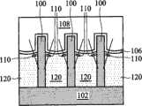
随着增加集成电路的缩小尺寸与增加对集成电路速度的高要求,晶体管必须具有较高的驱动电流与越来越小的尺寸。鳍式场效应晶体管(Finfield-effect transistor,FinFET)因此被发展。图1显示一常见鳍式场效应晶体管的剖面图,其中该剖面图由横跨鳍状物而非源极与漏极区来制作。将鳍状物100形成为垂直的硅鳍状物延伸高于基底102并用以形成源极与漏极区(未显示)及介于其间的通道区。鳍状物100的形成包括使基底102凹陷以形成凹陷处、以一介电材料填满凹陷处、执行一化学机械研磨(chemical mechanicalpolish,CMP)以移除介电材料高于鳍状物的超出部分,及使介电材料的顶部层凹陷以使于凹陷处中的介电材料的剩余部分形成浅沟槽隔离区(shallowtrench isolation,STI)120。浅沟槽隔离区120通常包括氧化硅。栅极108形成于鳍状物100上。形成栅极介电质106以分隔鳍状物100与栅极108。With the increasing downsizing of integrated circuits and the increasing high demands on the speed of integrated circuits, transistors must have higher drive currents and smaller and smaller sizes. Finfield-effect transistors (Finfield-effect transistors, FinFETs) have thus been developed. Figure 1 shows a cross-sectional view of a conventional FinFET, where the cross-section is fabricated across the fin instead of the source and drain regions.
寄生电容器110被产生于栅极108与鳍状物100之间,其中浅沟槽隔离区120作为寄生电容器110的绝缘体。寄生电容器110的电容值(capacitancevalue)为浅沟槽隔离区120的形状与浅沟槽隔离区120的材料(例如k值)的函数。寄生电容不利地影响分别的集成电路的性能并需要被减少。A
发明内容Contents of the invention
本发明的目的在于克服现有技术中的缺陷。The purpose of the present invention is to overcome the disadvantages of the prior art.
根据实施例的一态样,一种集成电路结构包括一基底,其具有一第一部分于一第一元件区中与一第二部分于一第二元件区中;以及两个隔离区于该第一元件区中且于该基底上。所述两个隔离区包括一第一介电材料其具有一第一k值。一半导体条介于所述两个隔离区之间并与所述两个隔离区邻接,随着该半导体条的一顶部部分形成一半导体鳍状物于所述两个隔离区的顶部表面上。一额外的隔离区于该第二元件区中且于该基底上。该额外的隔离区包括一第二介电材料其具有大于该第一k值的一第二k值。According to an aspect of the embodiment, an integrated circuit structure includes a substrate having a first portion in a first device region and a second portion in a second device region; and two isolation regions in the first device region. In a device area and on the substrate. The two isolation regions include a first dielectric material having a first k value. A semiconductor strip is interposed between and adjacent to the two isolation regions, with a top portion of the semiconductor strip forming a semiconductor fin on top surfaces of the two isolation regions. An additional isolation region is in the second device region and on the substrate. The additional isolation region includes a second dielectric material having a second k value greater than the first k value.
根据本发明另一实施例,一种集成电路结构,包括:According to another embodiment of the present invention, an integrated circuit structure includes:
一半导体基底,其包括一第一部分于一元件内区中与一第二部分于一元件间区中;A semiconductor substrate comprising a first portion in an inner region of an element and a second portion in an inter-element region;
一元件内浅沟槽隔离区于该半导体基底上,其中该元件内浅沟槽隔离区由具有一第一k值的一低介电常数介电材料所形成;an intra-device shallow trench isolation region on the semiconductor substrate, wherein the intra-device shallow trench isolation region is formed of a low-k dielectric material having a first k value;
一第一鳍式场效应晶体管,包括:A first FinFET, comprising:
一半导体鳍状物与该元件内浅沟槽隔离区邻接且于该元件内浅沟槽隔离区上;a semiconductor fin adjacent to and over the device STI region;
一栅极介电质于该半导体鳍状物上;以及a gate dielectric on the semiconductor fin; and
一栅极电极于该栅极介电质上,其中该栅极电极包括一部分直接于该元件内浅沟槽隔离区上;以及a gate electrode on the gate dielectric, wherein the gate electrode includes a portion directly on the shallow trench isolation region in the device; and
一元件间浅沟槽隔离区于该半导体基底上,其中没有栅极电极直接形成于该元件间浅沟槽隔离区上,且其中该元件间浅沟槽隔离由一非低介电常数介电材料所形成,该非低介电常数介电材料具有大于该第一k值的一第二k值。An inter-element shallow trench isolation region is on the semiconductor substrate, wherein no gate electrode is directly formed on the inter-element shallow trench isolation region, and wherein the inter-element shallow trench isolation is formed by a non-low-k dielectric The non-low-k dielectric material has a second k value greater than the first k value.
也公开其他实施例。Other embodiments are also disclosed.
通过使用低介电常数材料来形成元件内浅沟槽隔离区,减少了鳍式场效应晶体管的寄生栅极电容并且增加分别的鳍式场效应晶体管的速度。By using a low dielectric constant material to form the intra-device shallow trench isolation regions, the parasitic gate capacitance of the FinFETs is reduced and the speed of the respective FinFETs is increased.
为了让本发明的上述和其他目的、特征、和优点能更明显易懂,下文特举优选实施例,并配合附图,进行详细说明。In order to make the above and other objects, features, and advantages of the present invention more comprehensible, preferred embodiments are specifically cited below and described in detail with accompanying drawings.
附图说明Description of drawings
图1显示一常见鳍式场效应晶体管的剖面图;Figure 1 shows a cross-sectional view of a common FinFET;
图2至图10A为根据一实施例在鳍式场效应晶体管制造中的中间阶段的剖面图;2-10A are cross-sectional views of intermediate stages in the fabrication of FinFETs according to one embodiment;
图10B显示于图10A中所示结构的俯视图。Figure 10B shows a top view of the structure shown in Figure 10A.
其中,附图标记说明如下:Wherein, the reference signs are explained as follows:
100~鳍状物100~fins
102~基底102~base
106~栅极介电质106~Gate dielectric
108~栅极108~gate
110~寄生电容器110~parasitic capacitor
120~浅沟槽隔离区(shallow trench isolation,STI)120~shallow trench isolation (STI)
20~半导体基底20~semiconductor substrate
100~元件内区(intra-device region)100~intra-device region
200~元件间区(inter-device region)200~inter-device region
22~焊垫层22~pad layer
24~掩模层24~mask layer
26~光致抗蚀剂26 ~ photoresist
28~开口28 ~ opening
32~沟槽32~groove
D~沟槽32的深度D~depth of
W~沟槽32的宽度W~width of
33~半导体条33~semiconductor bar
34~低介电常数材料34~Low dielectric constant material
34’~元件内浅沟槽隔离区(intra-device shallow trench isolation region)34'~Intra-device shallow trench isolation region (intra-device shallow trench isolation region)
L1、L1’、L1”~元件内浅沟槽隔离区34’的长度L1, L1', L1"~the length of the shallow trench isolation region 34' in the component
38、45~凹陷处38, 45 ~ depression
40~鳍状物40 ~ fins
H~鳍状物40的高度H~the height of the fin 40
L2~鳍状物40的长度L2 ~ the length of the
44~硬掩模44 ~ hard mask
48、70、72~虚线48, 70, 72 ~ dotted line
50~介电材料50~dielectric material
50’~元件间浅沟槽隔离区(inter-device shallow trench isolation region)50'~inter-device shallow trench isolation region
62~栅极介电质62~Gate dielectric
64~栅极电极64~Gate electrode
66~鳍式场效应晶体管66~Fin Field Effect Transistor
80~电容器80~capacitor
具体实施方式Detailed ways
提供形成鳍式场效应晶体管(Fin field-effect transistor,FinFET)的新颖方法。以图解说明在一实施例的制造中的中间阶段。实施例的变化被讨论。遍及于不同附图与说明的实施例中,相同的标号用来代表相同的元件。Novel methods for forming Fin field-effect transistors (FinFETs) are provided. Intermediate stages in the manufacture of an embodiment are illustrated. Variations of embodiments are discussed. The same reference numerals are used to represent the same elements throughout the different drawings and illustrated embodiments.
参见图2,提供半导体基底20。在一实施例中,半导体基底20包括硅。其他一般使用的材料,例如碳、锗、镓、砷、氮、铟及/或磷与其类似物也可被包括于半导体基底20中。半导体基底20可为一块状基底(bulk substrate)或一绝缘层上半导体(semiconductor-on-insulator)基底。半导体基底20包括于元件内区(intra-device region)100的部分与元件间区(inter-device region)200的部分。可使用每个元件内区100来形成一鳍式场效应晶体管,同时可通过元件间区200来将元件内区100彼此分离,元件间区200可不具有鳍式场效应晶体管形成于其中。元件间区200可或可不直接介于两个鳍式场效应晶体管之间。Referring to FIG. 2, a
焊垫层22与掩模层24可形成于半导体基底20上。焊垫层22,可为例如使用热氧化工艺(thermal oxidation process)来形成的一包括氧化硅的薄膜。焊垫层22可作为介于半导体基底20与掩模层24之间的一附着层(adhesionlayer)。焊垫层22也可作为蚀刻掩模层24的一蚀刻终止层。在一实施例中,掩模层24为例如使用低压化学气相沉积(low pressure chemical vapordeposition,LPCVD)由氮化硅所形成。在其他实施例中,掩模层24通过硅的热氮化(thermal nitridation)、等离子体辅助化学气相沉积(plasma enhancedchemical vapor deposition,PECVD)或等离子体阳极氮化(plasma anodicnitridation)来形成。在随后的光微影(photolithography)工艺中将掩模层24作为一硬掩模。光致抗蚀剂26形成于掩模层24上且之后将其图案化,形成开口28于光致抗蚀剂26中。The
参见图3,经由开口28来蚀刻掩模层24与焊垫层22,露出下方的半导体基底20。之后蚀刻露出的半导体基底20以形成沟槽32与半导体条33,半导体条33为半导体基底20介于沟槽32之间的部分。沟槽32可为互相平行的条带(于俯视中)且被彼此紧密地设置。之后移除光致抗蚀剂26。接着可执行一清洁以移除半导体基底20的自生氧化层(native oxide)。可使用经稀释的氢氟酸(hydrofluoric acid,HF)来执行清洁。Referring to FIG. 3 , the
沟槽32的深度D可介于约


参见图4,将低介电常数材料34填入沟槽32中。视需要而定,可形成一衬底氧化层(liner oxide)(未显示)于沟槽32中。在一实施例中,衬底氧化层可为一热氧化层(thermal oxide)。在其他实施例中,可使用临场蒸气产生(in situ steam generation,ISSG)来形成衬底氧化层。在又其他实施例中,可使用选择区域化学气相沉积(selective area chemical vapor deposition,SACVD)或其他一般使用的化学气相沉积方法来形成衬底氧化层。衬底氧化层的形成环绕沟槽32的边角,其减低电场并因此改善所产生的集成电路的性能。Referring to FIG. 4 , the
低介电常数材料34具有一k值小于3.9。低介电常数材料34的k值也可小于约3.5、3.0、2.5,或甚至小于约2.0。在一实施例中,低介电常数材料34包括含碳的低介电常数材料。在其他实施例中,低介电常数材料包括其他一般已知低介电常数材料,例如硼磷硅玻璃(boro-phospho-silicate glass,BPSG)、磷硅玻璃(phospho-silicate glass,PSG)及/或其类似物。The low-
之后执行一化学机械研磨以使低介电常数材料34的顶部表面与掩模层24的顶部表面同水平。所产生的结构显示于图5中。之后通过一蚀刻步骤使低介电常数材料凹陷,产生如图6中所示的凹陷处38。焊垫层22与掩模层24的剩余部分也被移除。半导体条33延伸出剩余的低介电常数材料34的顶部表面的部分因此变成鳍状物40。鳍状物40的高度H可介于15nm与约50nm之间,然而其也可较大或较小。A CMP is then performed to level the top surface of the low-
接着,如图6中所示,形成硬掩模44以覆盖元件内区100,而留下元件间区200未覆盖,硬掩模44可由氮化硅所形成。之后执行一蚀刻工艺以自元件间区200移除低介电常数材料34的露出部分,形成凹陷处45,如图7中所示。低介电常数材料34在元件内区100中的部分不被移除,且于此之后被称为元件内浅沟槽隔离区(intra-device shallow trench isolationregion)34’。Next, as shown in FIG. 6 , a
在图8中,将介电材料50填入凹陷处45内。介电材料50具有一k值大于低介电常数材料34的k值。在一实施例中,介电材料50由一非低介电常数材料所形成,非低介电常数材料具有等于或大于3.9的k值。介电材料50的k值也可大于约5.0。在一示范实施例中,介电材料50包括氧化硅,其可由化学气相沉积,例如次常压化学气相沉积(sub-atmospheric CVD,SACVD)、高密度等离子体化学气相沉积(high density plasma CVD,HDPCVD)或其类似方法来形成。介电材料50的顶部表面为高于硬掩模44的顶部表面。In FIG. 8 , a
执行化学机械研磨以使介电材料50的顶部表面与硬掩模44的顶部表面呈水平。之后执行一蚀刻以更进一步使剩余的介电材料50的顶部表面凹陷。所产生的结构显示于图9中。于说明书全文中,介电材料50的剩余部分被二择一地称为元件间浅沟槽隔离区(inter-device shallow trench isolationregion)50’。在一实施例中,在蚀刻步骤之后,元件间浅沟槽隔离区50’的经凹陷的顶部表面实质上与元件内浅沟槽隔离区34’呈水平。在替代实施例中,如以虚线48所示,元件间浅沟槽隔离区50’的经凹陷的顶部表面实质上与鳍状物40的顶部表面呈水平,或在介于鳍状物40的表面与元件内浅沟槽隔离区34’的顶部表面之间的任何水平面。元件间浅沟槽隔离区50’与元件内浅沟槽隔离区34’的底部表面可彼此呈水平。之后移除硬掩模44。在产生的结构中,元件间浅沟槽隔离区50’与元件内浅沟槽隔离区34’也可被视为在半导体基底20上(尽管它们原始被形成于半导体基底20内)。Chemical mechanical polishing is performed to level the top surface of
虽然于上述实施例中,在形成元件间浅沟槽隔离区50’之前形成元件内浅沟槽隔离区34’,然而也可在形成元件间浅沟槽隔离区50’之后形成元件内浅沟槽隔离区34’。在此实施例中,在于图4中所示的步骤中,将非低介电常数材料50填入沟槽32。在步骤7与8中,将非低介电常数材料50的部分自元件内区100移除以形成凹陷处,并且将低介电常数材料34填入凹陷处中。本领域技术人员可了解通过于先前附图中所提供的实施教示。Although in the above-mentioned embodiment, the intra-device STI region 34' is formed before the inter-device STI region 50' is formed, the intra-device STI region 34' may also be formed after the inter-device STI region 50' is formed. Groove isolation region 34'. In this embodiment,
参见图10A,形成栅极介电质62以覆盖鳍状物40的顶部表面与侧壁。栅极介电质62可通过热氧化形成且因此可包括热氧化硅。于此实施例中,栅极介电质62被形成于鳍状物40的顶部表面上,而不在元件内浅沟槽隔离区34’的顶部表面上。或者,栅极介电质62可通过沉积步骤来形成。因此,栅极介电质62被形成于鳍状物40的顶部表面与元件内浅沟槽隔离区34’的顶部表面上。之后于栅极介电质62上形成栅极电极64。在一实施例中,如图10A中所示,栅极电极64不只覆盖鳍状物40,以使每个所产生的鳍式场效应晶体管66包括多于一个鳍状物40。在替代实施例中,每个鳍状物40可被用来形成一个鳍式场效应晶体管。Referring to FIG. 10A ,
图10B显示于图10A中所示结构的俯视图,其中图10A中的剖面图获得自于图10B中的平面横跨线10A-10A。观察到元件内浅沟槽隔离区34’可被元件间浅沟槽隔离区50’所包围。然而,随着分别由虚线70与72所示的对应边界,元件内浅沟槽隔离区34’的大小可为较大或较小。在一实施例中,元件内浅沟槽隔离区34’的长度L1等于鳍状物40的长度L2。在其他实施例中,如由虚线72所示,元件内浅沟槽隔离区34’的长度L1’小于鳍状物40的长度L2。在又其他实施例中,如由虚线70所示,元件内浅沟槽隔离区34’的长度L1”大于鳍状物40的长度L2。之后在鳍状物40不被栅极电极64覆盖的部分上形成鳍式场效应晶体管66的剩余构件,包括源极与漏极区及源极与漏极硅化物(未显示于图10A与图10B中)。这些构件的形成工艺为本技术领域所知,且因此不于此重复。Figure 10B shows a top view of the structure shown in Figure 10A, where the cross-sectional view in Figure 10A is taken from the plane across line 10A-10A in Figure 10B. It is observed that the intra-device STI region 34' may be surrounded by the inter-device STI region 50'. However, the size of the intra-device STI region 34' may be larger or smaller with corresponding boundaries shown by dashed lines 70 and 72, respectively. In one embodiment, the length L1 of the intra-device STI region 34' is equal to the length L2 of the
实施例具有一些优点特征。由于电容器的电容与电容器绝缘体的k值成比例,因此通过使用低介电常数材料来形成元件内浅沟槽隔离区,减少了鳍式场效应晶体管的寄生栅极电容(如图10A中的电容器80所示)并且增加分别的鳍式场效应晶体管的速度。然而,由于元件间浅沟槽隔离区仍可使用一般浅沟槽隔离材料来形成,因此可将由于在元件内浅沟槽隔离区中使用低介电常数材料所引起的应力最小化。Embodiments have some advantageous features. Since the capacitance of the capacitor is proportional to the k value of the capacitor insulator, the parasitic gate capacitance of the FinFET is reduced by using a low dielectric constant material to form the shallow trench isolation region in the device (such as the capacitor in Figure 10A 80) and increase the speed of the respective FinFETs. However, since the inter-device STI region can still be formed using general STI materials, the stress caused by using low dielectric constant material in the intra-device STI region can be minimized.
虽然本发明已以优选实施例揭露如上,然其并非用以限定本发明,任何本领域技术人员,在不脱离本发明的精神和范围内,当可作些许的更动与润饰,因此本发明的保护范围当视随附的权利要求所界定的保护范围为准。Although the present invention has been disclosed above with preferred embodiments, it is not intended to limit the present invention. Any person skilled in the art may make some changes and modifications without departing from the spirit and scope of the present invention. Therefore, the present invention The scope of protection should be subject to the scope of protection defined by the appended claims.
Claims (10)
Translated fromChineseApplications Claiming Priority (4)
| Application Number | Priority Date | Filing Date | Title |
|---|---|---|---|
| US25572409P | 2009-10-28 | 2009-10-28 | |
| US61/255,724 | 2009-10-28 | ||
| US12/843,658US8592918B2 (en) | 2009-10-28 | 2010-07-26 | Forming inter-device STI regions and intra-device STI regions using different dielectric materials |
| US12/843,658 | 2010-07-26 |
Publications (2)
| Publication Number | Publication Date |
|---|---|
| CN102074572Atrue CN102074572A (en) | 2011-05-25 |
| CN102074572B CN102074572B (en) | 2013-01-30 |
Family
ID=43897660
Family Applications (1)
| Application Number | Title | Priority Date | Filing Date |
|---|---|---|---|
| CN201010528793.6AActiveCN102074572B (en) | 2009-10-28 | 2010-10-25 | integrated circuit structure |
Country Status (5)
| Country | Link |
|---|---|
| US (2) | US8592918B2 (en) |
| JP (1) | JP5377456B2 (en) |
| KR (1) | KR101229709B1 (en) |
| CN (1) | CN102074572B (en) |
| TW (1) | TWI424528B (en) |
Cited By (7)
| Publication number | Priority date | Publication date | Assignee | Title |
|---|---|---|---|---|
| CN102437179A (en)* | 2011-12-07 | 2012-05-02 | 中国科学院上海微系统与信息技术研究所 | Layout structure of total dose radiation resistant reinforced deep submicron device |
| CN103828037A (en)* | 2011-07-29 | 2014-05-28 | 美商新思科技有限公司 | N-channel and P-channel finFET cell architecture with inter-block insulator |
| US9691764B2 (en) | 2011-07-29 | 2017-06-27 | Synopsys, Inc. | FinFET cell architecture with power traces |
| CN107293588A (en)* | 2016-03-30 | 2017-10-24 | 中芯国际集成电路制造(上海)有限公司 | Semiconductor device and its manufacture method |
| CN107731751A (en)* | 2016-08-12 | 2018-02-23 | 中芯国际集成电路制造(上海)有限公司 | Semiconductor structure and forming method thereof |
| CN104157604B (en)* | 2013-05-14 | 2018-03-20 | 格罗方德半导体公司 | Standard block and its preparation method for the dense pack of IC products |
| CN108074869A (en)* | 2016-11-14 | 2018-05-25 | 中芯国际集成电路制造(上海)有限公司 | Fin formula field effect transistor and forming method thereof |
Families Citing this family (29)
| Publication number | Priority date | Publication date | Assignee | Title |
|---|---|---|---|---|
| JP2010199161A (en)* | 2009-02-23 | 2010-09-09 | Renesas Electronics Corp | Semiconductor integrated circuit device and method of manufacturing the same |
| TWI587382B (en)* | 2011-10-19 | 2017-06-11 | 聯華電子股份有限公司 | Semiconductor structure and process thereof |
| US9893163B2 (en)* | 2011-11-04 | 2018-02-13 | Taiwan Semiconductor Manufacturing Company, Ltd. | 3D capacitor and method of manufacturing same |
| US9318431B2 (en)* | 2011-11-04 | 2016-04-19 | Taiwan Semiconductor Manufacturing Company, Ltd. | Integrated circuit having a MOM capacitor and method of making same |
| US8735991B2 (en)* | 2011-12-01 | 2014-05-27 | Taiwan Semiconductor Manufacturing Company, Ltd. | High gate density devices and methods |
| WO2013101219A1 (en) | 2011-12-30 | 2013-07-04 | Intel Corporation | Wrap-around trench contact structure and methods of fabrication |
| US8969974B2 (en) | 2012-06-14 | 2015-03-03 | Taiwan Semiconductor Manufacturing Company, Ltd. | Structure and method for FinFET device |
| US8946014B2 (en)* | 2012-12-28 | 2015-02-03 | Taiwan Semiconductor Manufacturing Company, Ltd. | FinFET device structure and methods of making same |
| US9093566B2 (en)* | 2012-12-31 | 2015-07-28 | Taiwan Semiconductor Manufacturing Company, Ltd. | High efficiency FinFET diode |
| US9000522B2 (en)* | 2013-01-09 | 2015-04-07 | International Business Machines Corporation | FinFET with dielectric isolation by silicon-on-nothing and method of fabrication |
| KR102013842B1 (en)* | 2013-02-08 | 2019-08-26 | 삼성전자주식회사 | Method of manufacturing semiconductor device |
| US8895446B2 (en) | 2013-02-18 | 2014-11-25 | Taiwan Semiconductor Manufacturing Company, Ltd. | Fin deformation modulation |
| US9953975B2 (en) | 2013-07-19 | 2018-04-24 | Taiwan Semiconductor Manufacturing Company, Ltd. | Methods for forming STI regions in integrated circuits |
| US9023705B1 (en)* | 2013-11-01 | 2015-05-05 | Globalfoundries Inc. | Methods of forming stressed multilayer FinFET devices with alternative channel materials |
| US9209178B2 (en)* | 2013-11-25 | 2015-12-08 | International Business Machines Corporation | finFET isolation by selective cyclic etch |
| US9196499B2 (en)* | 2014-03-26 | 2015-11-24 | Globalfoundries Inc. | Method of forming semiconductor fins |
| US9842944B2 (en) | 2014-07-14 | 2017-12-12 | Intel Corporation | Solid-source diffused junction for fin-based electronics |
| US9236308B1 (en)* | 2014-08-19 | 2016-01-12 | Globalfoundries Inc. | Methods of fabricating fin structures of uniform height |
| KR102204387B1 (en)* | 2014-12-17 | 2021-01-18 | 삼성전자주식회사 | Semiconductor device having buried gate structure and method of fabricating the same |
| US9461043B1 (en)* | 2015-03-20 | 2016-10-04 | Taiwan Semiconductor Manufacturing Co., Ltd. | Semiconductor device and manufacturing method thereof |
| US9793403B2 (en) | 2015-04-14 | 2017-10-17 | Samsung Electronics Co., Ltd. | Multi-layer fin field effect transistor devices and methods of forming the same |
| KR102393321B1 (en) | 2015-06-25 | 2022-04-29 | 삼성전자주식회사 | Semiconductor device and method for fabricating the same |
| KR102323943B1 (en) | 2015-10-21 | 2021-11-08 | 삼성전자주식회사 | Method of manufacturing semiconductor device |
| WO2017111816A1 (en)* | 2015-12-26 | 2017-06-29 | Intel Corporation | Confined and scalable helmet |
| US9704994B1 (en)* | 2016-10-10 | 2017-07-11 | International Business Machines Corporation | Different shallow trench isolation fill in fin and non-fin regions of finFET |
| US9899396B1 (en)* | 2016-12-01 | 2018-02-20 | Macronix International Co., Ltd. | Semiconductor device, fabricating method thereof, and fabricating method of memory |
| WO2019066768A1 (en)* | 2017-09-26 | 2019-04-04 | Intel Corporation | Directional spacer removal for integrated circuit structures |
| KR20230006054A (en)* | 2017-11-30 | 2023-01-10 | 인텔 코포레이션 | Fin patterning for advanced integrated circuit structure fabrication |
| US11004748B2 (en)* | 2019-06-05 | 2021-05-11 | Globalfoundries U.S. Inc. | Semiconductor devices with wide gate-to-gate spacing |
Citations (4)
| Publication number | Priority date | Publication date | Assignee | Title |
|---|---|---|---|---|
| US20020011612A1 (en)* | 2000-07-31 | 2002-01-31 | Kabushiki Kaisha Toshiba | Semiconductor device and method for manufacturing the same |
| US20070228425A1 (en)* | 2006-04-04 | 2007-10-04 | Miller Gayle W | Method and manufacturing low leakage MOSFETs and FinFETs |
| US20080081404A1 (en)* | 2006-09-29 | 2008-04-03 | Texas Instruments Incorporated | Recessed STI for wide transistors |
| US20090008716A1 (en)* | 2007-06-27 | 2009-01-08 | Kabushiki Kaisha Toshiba | Semiconductor device and method of fabricating the same |
Family Cites Families (21)
| Publication number | Priority date | Publication date | Assignee | Title |
|---|---|---|---|---|
| JPH11163329A (en) | 1997-11-27 | 1999-06-18 | Mitsubishi Electric Corp | Semiconductor device and manufacturing method thereof |
| US7358121B2 (en) | 2002-08-23 | 2008-04-15 | Intel Corporation | Tri-gate devices and methods of fabrication |
| US6706571B1 (en) | 2002-10-22 | 2004-03-16 | Advanced Micro Devices, Inc. | Method for forming multiple structures in a semiconductor device |
| KR100513405B1 (en) | 2003-12-16 | 2005-09-09 | 삼성전자주식회사 | Method for forming fin field effect transistor |
| JP5170958B2 (en) | 2004-01-30 | 2013-03-27 | ルネサスエレクトロニクス株式会社 | Field effect transistor and manufacturing method thereof |
| JPWO2006006438A1 (en) | 2004-07-12 | 2008-04-24 | 日本電気株式会社 | Semiconductor device and manufacturing method thereof |
| US20060134846A1 (en)* | 2004-12-16 | 2006-06-22 | Macronix International Co., Ltd. | Method of fabricating a semiconductor structure |
| JP2006269975A (en)* | 2005-03-25 | 2006-10-05 | Toshiba Corp | Semiconductor device and manufacturing method thereof |
| US7859065B2 (en)* | 2005-06-07 | 2010-12-28 | Nec Corporation | Fin-type field effect transistor and semiconductor device |
| US7247887B2 (en) | 2005-07-01 | 2007-07-24 | Synopsys, Inc. | Segmented channel MOS transistor |
| US7508031B2 (en) | 2005-07-01 | 2009-03-24 | Synopsys, Inc. | Enhanced segmented channel MOS transistor with narrowed base regions |
| US7807523B2 (en) | 2005-07-01 | 2010-10-05 | Synopsys, Inc. | Sequential selective epitaxial growth |
| US7605449B2 (en) | 2005-07-01 | 2009-10-20 | Synopsys, Inc. | Enhanced segmented channel MOS transistor with high-permittivity dielectric isolation material |
| US7265008B2 (en) | 2005-07-01 | 2007-09-04 | Synopsys, Inc. | Method of IC production using corrugated substrate |
| US7190050B2 (en) | 2005-07-01 | 2007-03-13 | Synopsys, Inc. | Integrated circuit on corrugated substrate |
| US8466490B2 (en) | 2005-07-01 | 2013-06-18 | Synopsys, Inc. | Enhanced segmented channel MOS transistor with multi layer regions |
| KR100657964B1 (en)* | 2005-07-22 | 2006-12-14 | 삼성전자주식회사 | Random access memory and semiconductor device having a single gate electrode corresponding to a pair of pin-type channel regions |
| JP2007180362A (en)* | 2005-12-28 | 2007-07-12 | Toshiba Corp | Semiconductor device |
| US20080157225A1 (en)* | 2006-12-29 | 2008-07-03 | Suman Datta | SRAM and logic transistors with variable height multi-gate transistor architecture |
| US7939862B2 (en) | 2007-05-30 | 2011-05-10 | Synopsys, Inc. | Stress-enhanced performance of a FinFet using surface/channel orientations and strained capping layers |
| EP2073267A1 (en)* | 2007-12-19 | 2009-06-24 | INTERUNIVERSITAIR MICROELEKTRONICA CENTRUM vzw (IMEC) | Method of fabricating multi-gate semiconductor devices and devices obtained |
- 2010
- 2010-07-26USUS12/843,658patent/US8592918B2/enactiveActive
- 2010-10-14TWTW099135019Apatent/TWI424528B/enactive
- 2010-10-25CNCN201010528793.6Apatent/CN102074572B/enactiveActive
- 2010-10-25KRKR1020100104320Apatent/KR101229709B1/enactiveActive
- 2010-10-27JPJP2010240536Apatent/JP5377456B2/enactiveActive
- 2013
- 2013-09-05USUS14/019,338patent/US8846466B2/enactiveActive
Patent Citations (4)
| Publication number | Priority date | Publication date | Assignee | Title |
|---|---|---|---|---|
| US20020011612A1 (en)* | 2000-07-31 | 2002-01-31 | Kabushiki Kaisha Toshiba | Semiconductor device and method for manufacturing the same |
| US20070228425A1 (en)* | 2006-04-04 | 2007-10-04 | Miller Gayle W | Method and manufacturing low leakage MOSFETs and FinFETs |
| US20080081404A1 (en)* | 2006-09-29 | 2008-04-03 | Texas Instruments Incorporated | Recessed STI for wide transistors |
| US20090008716A1 (en)* | 2007-06-27 | 2009-01-08 | Kabushiki Kaisha Toshiba | Semiconductor device and method of fabricating the same |
Cited By (12)
| Publication number | Priority date | Publication date | Assignee | Title |
|---|---|---|---|---|
| CN103828037A (en)* | 2011-07-29 | 2014-05-28 | 美商新思科技有限公司 | N-channel and P-channel finFET cell architecture with inter-block insulator |
| CN103828037B (en)* | 2011-07-29 | 2017-03-01 | 美商新思科技有限公司 | There is the N-channel of insulator and P-channel FINFET unit structure between block |
| US9691764B2 (en) | 2011-07-29 | 2017-06-27 | Synopsys, Inc. | FinFET cell architecture with power traces |
| US10990722B2 (en) | 2011-07-29 | 2021-04-27 | Synopsys, Inc. | FinFET cell architecture with insulator structure |
| CN102437179A (en)* | 2011-12-07 | 2012-05-02 | 中国科学院上海微系统与信息技术研究所 | Layout structure of total dose radiation resistant reinforced deep submicron device |
| CN104157604B (en)* | 2013-05-14 | 2018-03-20 | 格罗方德半导体公司 | Standard block and its preparation method for the dense pack of IC products |
| CN107293588A (en)* | 2016-03-30 | 2017-10-24 | 中芯国际集成电路制造(上海)有限公司 | Semiconductor device and its manufacture method |
| US10608112B2 (en) | 2016-03-30 | 2020-03-31 | Semiconductor Manufacturing International (Beijing) Corporation | FinFET device having FinFET structure and filled recesses that partially extend underneath the Fin structure |
| CN107731751A (en)* | 2016-08-12 | 2018-02-23 | 中芯国际集成电路制造(上海)有限公司 | Semiconductor structure and forming method thereof |
| CN107731751B (en)* | 2016-08-12 | 2020-06-09 | 中芯国际集成电路制造(上海)有限公司 | Semiconductor structure and forming method thereof |
| CN108074869A (en)* | 2016-11-14 | 2018-05-25 | 中芯国际集成电路制造(上海)有限公司 | Fin formula field effect transistor and forming method thereof |
| US10707134B2 (en) | 2016-11-14 | 2020-07-07 | Semiconductor Manufacturing International (Shanghai) Corporation | Fin field-effect transistor and fabrication method thereof |
Also Published As
| Publication number | Publication date |
|---|---|
| US8592918B2 (en) | 2013-11-26 |
| US20140004682A1 (en) | 2014-01-02 |
| JP5377456B2 (en) | 2013-12-25 |
| CN102074572B (en) | 2013-01-30 |
| TW201133704A (en) | 2011-10-01 |
| US8846466B2 (en) | 2014-09-30 |
| KR101229709B1 (en) | 2013-02-05 |
| KR20110049679A (en) | 2011-05-12 |
| TWI424528B (en) | 2014-01-21 |
| JP2011097058A (en) | 2011-05-12 |
| US20110095372A1 (en) | 2011-04-28 |
Similar Documents
| Publication | Publication Date | Title |
|---|---|---|
| CN102074572B (en) | integrated circuit structure | |
| JP5836437B2 (en) | Method for forming an integrated circuit structure | |
| TWI430446B (en) | Integrated circuit structure and forming method thereof | |
| CN103985711B (en) | FinFETs with reduced parasitic capacitance and methods of forming the same | |
| TWI711086B (en) | Method for fabricating fin field effect transistor(finfet), semiconductor device and method for fabricating the same | |
| US9640441B2 (en) | Voids in STI regions for forming bulk FinFETs | |
| CN103187304B (en) | Manufacture the method for semiconductor device and transistor | |
| TWI717405B (en) | Fin field effect transistor and semiconductor structure | |
| CN101577278A (en) | Semiconductor structure and forming method thereof | |
| CN106711142A (en) | Fin field effect transistor and manufacturing method thereof | |
| CN105702727A (en) | Metal oxide semiconductor device and forming method thereof | |
| CN105826379B (en) | Semiconductor structure and method of making the same | |
| TWI715132B (en) | Integrated circuit and manufacturing method thereof | |
| KR101163909B1 (en) | Sti shape near fin bottom of si fin in bulk finfet | |
| CN104952923A (en) | Semiconductor device and manufacturing method thereof |
Legal Events
| Date | Code | Title | Description |
|---|---|---|---|
| C06 | Publication | ||
| PB01 | Publication | ||
| C10 | Entry into substantive examination | ||
| SE01 | Entry into force of request for substantive examination | ||
| C14 | Grant of patent or utility model | ||
| GR01 | Patent grant |