CN102074461B - Semiconductor device and manufacturing method thereof - Google Patents
Semiconductor device and manufacturing method thereofDownload PDFInfo
- Publication number
- CN102074461B CN102074461BCN201010518047.9ACN201010518047ACN102074461BCN 102074461 BCN102074461 BCN 102074461BCN 201010518047 ACN201010518047 ACN 201010518047ACN 102074461 BCN102074461 BCN 102074461B
- Authority
- CN
- China
- Prior art keywords
- crystal plane
- substrate
- plane direction
- semiconductor device
- semiconductor
- Prior art date
- Legal status (The legal status is an assumption and is not a legal conclusion. Google has not performed a legal analysis and makes no representation as to the accuracy of the status listed.)
- Active
Links
- 239000004065semiconductorSubstances0.000titleclaimsabstractdescription80
- 238000004519manufacturing processMethods0.000titleclaimsabstractdescription22
- 238000000034methodMethods0.000claimsabstractdescription144
- 239000000758substrateSubstances0.000claimsabstractdescription75
- 239000013078crystalSubstances0.000claimsabstractdescription50
- 238000005530etchingMethods0.000claimsabstractdescription42
- 239000000463materialSubstances0.000claimsabstractdescription17
- GNPVGFCGXDBREM-UHFFFAOYSA-Ngermanium atomChemical compound[Ge]GNPVGFCGXDBREM-UHFFFAOYSA-N0.000claimsdescription37
- 229910052732germaniumInorganic materials0.000claimsdescription36
- 229910052710siliconInorganic materials0.000claimsdescription22
- 239000010703siliconSubstances0.000claimsdescription22
- 230000007547defectEffects0.000claimsdescription10
- 239000000460chlorineSubstances0.000claimsdescription7
- 238000000407epitaxyMethods0.000claimsdescription5
- WKBOTKDWSSQWDR-UHFFFAOYSA-NBromine atomChemical compound[Br]WKBOTKDWSSQWDR-UHFFFAOYSA-N0.000claimsdescription3
- ZAMOUSCENKQFHK-UHFFFAOYSA-NChlorine atomChemical compound[Cl]ZAMOUSCENKQFHK-UHFFFAOYSA-N0.000claimsdescription3
- GDTBXPJZTBHREO-UHFFFAOYSA-NbromineSubstancesBrBrGDTBXPJZTBHREO-UHFFFAOYSA-N0.000claimsdescription3
- 229910052794bromiumInorganic materials0.000claimsdescription3
- 229910052801chlorineInorganic materials0.000claimsdescription3
- 239000010410layerSubstances0.000description73
- 239000007789gasSubstances0.000description21
- XUIMIQQOPSSXEZ-UHFFFAOYSA-NSiliconChemical compound[Si]XUIMIQQOPSSXEZ-UHFFFAOYSA-N0.000description20
- 238000005229chemical vapour depositionMethods0.000description15
- 238000002955isolationMethods0.000description14
- 150000004767nitridesChemical class0.000description13
- 229920002120photoresistant polymerPolymers0.000description10
- 238000005240physical vapour depositionMethods0.000description10
- 238000000231atomic layer depositionMethods0.000description8
- 229910021420polycrystalline siliconInorganic materials0.000description8
- 229920005591polysiliconPolymers0.000description8
- 125000006850spacer groupChemical group0.000description8
- HBMJWWWQQXIZIP-UHFFFAOYSA-Nsilicon carbideChemical compound[Si+]#[C-]HBMJWWWQQXIZIP-UHFFFAOYSA-N0.000description7
- 229910052581Si3N4Inorganic materials0.000description6
- 229910000577Silicon-germaniumInorganic materials0.000description6
- 229910052751metalInorganic materials0.000description6
- 239000002184metalSubstances0.000description6
- HQVNEWCFYHHQES-UHFFFAOYSA-Nsilicon nitrideChemical compoundN12[Si]34N5[Si]62N3[Si]51N64HQVNEWCFYHHQES-UHFFFAOYSA-N0.000description6
- 238000002513implantationMethods0.000description5
- 238000000206photolithographyMethods0.000description5
- 239000003989dielectric materialSubstances0.000description4
- 238000001312dry etchingMethods0.000description4
- KRHYYFGTRYWZRS-UHFFFAOYSA-Nhydrofluoric acidSubstancesFKRHYYFGTRYWZRS-UHFFFAOYSA-N0.000description4
- 239000012212insulatorSubstances0.000description4
- 229910021332silicideInorganic materials0.000description4
- 229910010271silicon carbideInorganic materials0.000description4
- VYPSYNLAJGMNEJ-UHFFFAOYSA-NSilicium dioxideChemical compoundO=[Si]=OVYPSYNLAJGMNEJ-UHFFFAOYSA-N0.000description3
- LEVVHYCKPQWKOP-UHFFFAOYSA-N[Si].[Ge]Chemical compound[Si].[Ge]LEVVHYCKPQWKOP-UHFFFAOYSA-N0.000description3
- 230000015572biosynthetic processEffects0.000description3
- 150000001875compoundsChemical class0.000description3
- 239000002019doping agentSubstances0.000description3
- 230000005669field effectEffects0.000description3
- 238000011049fillingMethods0.000description3
- FVBUAEGBCNSCDD-UHFFFAOYSA-Nsilicide(4-)Chemical compound[Si-4]FVBUAEGBCNSCDD-UHFFFAOYSA-N0.000description3
- 229910052814silicon oxideInorganic materials0.000description3
- 239000000126substanceSubstances0.000description3
- ZOXJGFHDIHLPTG-UHFFFAOYSA-NBoronChemical compound[B]ZOXJGFHDIHLPTG-UHFFFAOYSA-N0.000description2
- RYGMFSIKBFXOCR-UHFFFAOYSA-NCopperChemical compound[Cu]RYGMFSIKBFXOCR-UHFFFAOYSA-N0.000description2
- YCKRFDGAMUMZLT-UHFFFAOYSA-NFluorine atomChemical compound[F]YCKRFDGAMUMZLT-UHFFFAOYSA-N0.000description2
- VEXZGXHMUGYJMC-UHFFFAOYSA-NHydrochloric acidChemical compoundClVEXZGXHMUGYJMC-UHFFFAOYSA-N0.000description2
- -1LaSiOInorganic materials0.000description2
- NBIIXXVUZAFLBC-UHFFFAOYSA-NPhosphoric acidChemical compoundOP(O)(O)=ONBIIXXVUZAFLBC-UHFFFAOYSA-N0.000description2
- 229910052785arsenicInorganic materials0.000description2
- RQNWIZPPADIBDY-UHFFFAOYSA-Narsenic atomChemical compound[As]RQNWIZPPADIBDY-UHFFFAOYSA-N0.000description2
- QVGXLLKOCUKJST-UHFFFAOYSA-Natomic oxygenChemical compound[O]QVGXLLKOCUKJST-UHFFFAOYSA-N0.000description2
- 229910052796boronInorganic materials0.000description2
- 229910052802copperInorganic materials0.000description2
- 239000010949copperSubstances0.000description2
- 238000000151depositionMethods0.000description2
- 230000000694effectsEffects0.000description2
- 229910052731fluorineInorganic materials0.000description2
- 239000011737fluorineSubstances0.000description2
- 229910052738indiumInorganic materials0.000description2
- WPYVAWXEWQSOGY-UHFFFAOYSA-Nindium antimonideChemical compound[Sb]#[In]WPYVAWXEWQSOGY-UHFFFAOYSA-N0.000description2
- APFVFJFRJDLVQX-UHFFFAOYSA-Nindium atomChemical compound[In]APFVFJFRJDLVQX-UHFFFAOYSA-N0.000description2
- 239000011810insulating materialSubstances0.000description2
- 239000011229interlayerSubstances0.000description2
- 238000004518low pressure chemical vapour depositionMethods0.000description2
- 230000000873masking effectEffects0.000description2
- QPJSUIGXIBEQAC-UHFFFAOYSA-Nn-(2,4-dichloro-5-propan-2-yloxyphenyl)acetamideChemical compoundCC(C)OC1=CC(NC(C)=O)=C(Cl)C=C1ClQPJSUIGXIBEQAC-UHFFFAOYSA-N0.000description2
- 230000003647oxidationEffects0.000description2
- 238000007254oxidation reactionMethods0.000description2
- 239000001301oxygenSubstances0.000description2
- 229910052760oxygenInorganic materials0.000description2
- 238000001020plasma etchingMethods0.000description2
- 238000000623plasma-assisted chemical vapour depositionMethods0.000description2
- 238000005498polishingMethods0.000description2
- 229910018072Al 2 O 3Inorganic materials0.000description1
- 229910017121AlSiOInorganic materials0.000description1
- JBRZTFJDHDCESZ-UHFFFAOYSA-NAsGaChemical compound[As]#[Ga]JBRZTFJDHDCESZ-UHFFFAOYSA-N0.000description1
- 229910004129HfSiOInorganic materials0.000description1
- 229910000673Indium arsenideInorganic materials0.000description1
- CBENFWSGALASAD-UHFFFAOYSA-NOzoneChemical compound[O-][O+]=OCBENFWSGALASAD-UHFFFAOYSA-N0.000description1
- OAICVXFJPJFONN-UHFFFAOYSA-NPhosphorusChemical compound[P]OAICVXFJPJFONN-UHFFFAOYSA-N0.000description1
- 229910004298SiO 2Inorganic materials0.000description1
- BLRPTPMANUNPDV-UHFFFAOYSA-NSilaneChemical compound[SiH4]BLRPTPMANUNPDV-UHFFFAOYSA-N0.000description1
- 229910002367SrTiOInorganic materials0.000description1
- 230000002411adverseEffects0.000description1
- 229910000147aluminium phosphateInorganic materials0.000description1
- 238000000137annealingMethods0.000description1
- 239000012159carrier gasSubstances0.000description1
- 238000004140cleaningMethods0.000description1
- 239000011248coating agentSubstances0.000description1
- 238000000576coating methodMethods0.000description1
- 239000004020conductorSubstances0.000description1
- 239000002178crystalline materialSubstances0.000description1
- 229910021419crystalline siliconInorganic materials0.000description1
- 238000002425crystallisationMethods0.000description1
- 230000008025crystallizationEffects0.000description1
- 230000002950deficientEffects0.000description1
- 230000008021depositionEffects0.000description1
- 238000010894electron beam technologyMethods0.000description1
- BHEPBYXIRTUNPN-UHFFFAOYSA-Nhydridophosphorus(.) (triplet)Chemical compound[PH]BHEPBYXIRTUNPN-UHFFFAOYSA-N0.000description1
- 238000011065in-situ storageMethods0.000description1
- RPQDHPTXJYYUPQ-UHFFFAOYSA-Nindium arsenideChemical compound[In]#[As]RPQDHPTXJYYUPQ-UHFFFAOYSA-N0.000description1
- 230000010354integrationEffects0.000description1
- 238000005468ion implantationMethods0.000description1
- 238000010884ion-beam techniqueMethods0.000description1
- 230000008018meltingEffects0.000description1
- 238000002844meltingMethods0.000description1
- 229910044991metal oxideInorganic materials0.000description1
- 150000004706metal oxidesChemical class0.000description1
- 238000012986modificationMethods0.000description1
- 230000004048modificationEffects0.000description1
- 238000000059patterningMethods0.000description1
- 229910052698phosphorusInorganic materials0.000description1
- 239000011574phosphorusSubstances0.000description1
- 239000002243precursorSubstances0.000description1
- 229910000077silaneInorganic materials0.000description1
- WFKWXMTUELFFGS-UHFFFAOYSA-NtungstenChemical compound[W]WFKWXMTUELFFGS-UHFFFAOYSA-N0.000description1
- 229910052721tungstenInorganic materials0.000description1
- 239000010937tungstenSubstances0.000description1
- 238000001039wet etchingMethods0.000description1
Images


Classifications
- H—ELECTRICITY
- H10—SEMICONDUCTOR DEVICES; ELECTRIC SOLID-STATE DEVICES NOT OTHERWISE PROVIDED FOR
- H10D—INORGANIC ELECTRIC SEMICONDUCTOR DEVICES
- H10D30/00—Field-effect transistors [FET]
- H10D30/60—Insulated-gate field-effect transistors [IGFET]
- H10D30/791—Arrangements for exerting mechanical stress on the crystal lattice of the channel regions
- H10D30/797—Arrangements for exerting mechanical stress on the crystal lattice of the channel regions being in source or drain regions, e.g. SiGe source or drain
- H—ELECTRICITY
- H01—ELECTRIC ELEMENTS
- H01L—SEMICONDUCTOR DEVICES NOT COVERED BY CLASS H10
- H01L21/00—Processes or apparatus adapted for the manufacture or treatment of semiconductor or solid state devices or of parts thereof
- H01L21/02—Manufacture or treatment of semiconductor devices or of parts thereof
- H01L21/02104—Forming layers
- H01L21/02365—Forming inorganic semiconducting materials on a substrate
- H01L21/02367—Substrates
- H01L21/0237—Materials
- H01L21/02373—Group 14 semiconducting materials
- H01L21/02381—Silicon, silicon germanium, germanium
- H—ELECTRICITY
- H01—ELECTRIC ELEMENTS
- H01L—SEMICONDUCTOR DEVICES NOT COVERED BY CLASS H10
- H01L21/00—Processes or apparatus adapted for the manufacture or treatment of semiconductor or solid state devices or of parts thereof
- H01L21/02—Manufacture or treatment of semiconductor devices or of parts thereof
- H01L21/02104—Forming layers
- H01L21/02365—Forming inorganic semiconducting materials on a substrate
- H01L21/02367—Substrates
- H01L21/02433—Crystal orientation
- H—ELECTRICITY
- H01—ELECTRIC ELEMENTS
- H01L—SEMICONDUCTOR DEVICES NOT COVERED BY CLASS H10
- H01L21/00—Processes or apparatus adapted for the manufacture or treatment of semiconductor or solid state devices or of parts thereof
- H01L21/02—Manufacture or treatment of semiconductor devices or of parts thereof
- H01L21/02104—Forming layers
- H01L21/02365—Forming inorganic semiconducting materials on a substrate
- H01L21/02518—Deposited layers
- H01L21/02521—Materials
- H01L21/02524—Group 14 semiconducting materials
- H01L21/02532—Silicon, silicon germanium, germanium
- H—ELECTRICITY
- H01—ELECTRIC ELEMENTS
- H01L—SEMICONDUCTOR DEVICES NOT COVERED BY CLASS H10
- H01L21/00—Processes or apparatus adapted for the manufacture or treatment of semiconductor or solid state devices or of parts thereof
- H01L21/02—Manufacture or treatment of semiconductor devices or of parts thereof
- H01L21/02104—Forming layers
- H01L21/02365—Forming inorganic semiconducting materials on a substrate
- H01L21/02612—Formation types
- H01L21/02617—Deposition types
- H01L21/02636—Selective deposition, e.g. simultaneous growth of mono- and non-monocrystalline semiconductor materials
- H01L21/02639—Preparation of substrate for selective deposition
- H—ELECTRICITY
- H01—ELECTRIC ELEMENTS
- H01L—SEMICONDUCTOR DEVICES NOT COVERED BY CLASS H10
- H01L21/00—Processes or apparatus adapted for the manufacture or treatment of semiconductor or solid state devices or of parts thereof
- H01L21/02—Manufacture or treatment of semiconductor devices or of parts thereof
- H01L21/04—Manufacture or treatment of semiconductor devices or of parts thereof the devices having potential barriers, e.g. a PN junction, depletion layer or carrier concentration layer
- H01L21/18—Manufacture or treatment of semiconductor devices or of parts thereof the devices having potential barriers, e.g. a PN junction, depletion layer or carrier concentration layer the devices having semiconductor bodies comprising elements of Group IV of the Periodic Table or AIIIBV compounds with or without impurities, e.g. doping materials
- H01L21/30—Treatment of semiconductor bodies using processes or apparatus not provided for in groups H01L21/20 - H01L21/26
- H01L21/302—Treatment of semiconductor bodies using processes or apparatus not provided for in groups H01L21/20 - H01L21/26 to change their surface-physical characteristics or shape, e.g. etching, polishing, cutting
- H01L21/306—Chemical or electrical treatment, e.g. electrolytic etching
- H01L21/3065—Plasma etching; Reactive-ion etching
- H—ELECTRICITY
- H10—SEMICONDUCTOR DEVICES; ELECTRIC SOLID-STATE DEVICES NOT OTHERWISE PROVIDED FOR
- H10D—INORGANIC ELECTRIC SEMICONDUCTOR DEVICES
- H10D30/00—Field-effect transistors [FET]
- H10D30/01—Manufacture or treatment
- H10D30/021—Manufacture or treatment of FETs having insulated gates [IGFET]
- H10D30/024—Manufacture or treatment of FETs having insulated gates [IGFET] of fin field-effect transistors [FinFET]
- H—ELECTRICITY
- H10—SEMICONDUCTOR DEVICES; ELECTRIC SOLID-STATE DEVICES NOT OTHERWISE PROVIDED FOR
- H10D—INORGANIC ELECTRIC SEMICONDUCTOR DEVICES
- H10D30/00—Field-effect transistors [FET]
- H10D30/60—Insulated-gate field-effect transistors [IGFET]
- H10D30/62—Fin field-effect transistors [FinFET]
- H10D30/6211—Fin field-effect transistors [FinFET] having fin-shaped semiconductor bodies integral with the bulk semiconductor substrates
- H—ELECTRICITY
- H10—SEMICONDUCTOR DEVICES; ELECTRIC SOLID-STATE DEVICES NOT OTHERWISE PROVIDED FOR
- H10D—INORGANIC ELECTRIC SEMICONDUCTOR DEVICES
- H10D62/00—Semiconductor bodies, or regions thereof, of devices having potential barriers
- H10D62/01—Manufacture or treatment
- H10D62/021—Forming source or drain recesses by etching e.g. recessing by etching and then refilling
- H—ELECTRICITY
- H10—SEMICONDUCTOR DEVICES; ELECTRIC SOLID-STATE DEVICES NOT OTHERWISE PROVIDED FOR
- H10D—INORGANIC ELECTRIC SEMICONDUCTOR DEVICES
- H10D62/00—Semiconductor bodies, or regions thereof, of devices having potential barriers
- H10D62/40—Crystalline structures
- H10D62/405—Orientations of crystalline planes
- H—ELECTRICITY
- H10—SEMICONDUCTOR DEVICES; ELECTRIC SOLID-STATE DEVICES NOT OTHERWISE PROVIDED FOR
- H10D—INORGANIC ELECTRIC SEMICONDUCTOR DEVICES
- H10D62/00—Semiconductor bodies, or regions thereof, of devices having potential barriers
- H10D62/50—Physical imperfections
- H10D62/53—Physical imperfections the imperfections being within the semiconductor body
- H—ELECTRICITY
- H10—SEMICONDUCTOR DEVICES; ELECTRIC SOLID-STATE DEVICES NOT OTHERWISE PROVIDED FOR
- H10D—INORGANIC ELECTRIC SEMICONDUCTOR DEVICES
- H10D62/00—Semiconductor bodies, or regions thereof, of devices having potential barriers
- H10D62/80—Semiconductor bodies, or regions thereof, of devices having potential barriers characterised by the materials
- H10D62/82—Heterojunctions
- H10D62/822—Heterojunctions comprising only Group IV materials heterojunctions, e.g. Si/Ge heterojunctions
- H—ELECTRICITY
- H10—SEMICONDUCTOR DEVICES; ELECTRIC SOLID-STATE DEVICES NOT OTHERWISE PROVIDED FOR
- H10D—INORGANIC ELECTRIC SEMICONDUCTOR DEVICES
- H10D62/00—Semiconductor bodies, or regions thereof, of devices having potential barriers
- H10D62/80—Semiconductor bodies, or regions thereof, of devices having potential barriers characterised by the materials
- H10D62/83—Semiconductor bodies, or regions thereof, of devices having potential barriers characterised by the materials being Group IV materials, e.g. B-doped Si or undoped Ge
- H10D62/832—Semiconductor bodies, or regions thereof, of devices having potential barriers characterised by the materials being Group IV materials, e.g. B-doped Si or undoped Ge being Group IV materials comprising two or more elements, e.g. SiGe
- H10D62/8325—Silicon carbide
- H—ELECTRICITY
- H10—SEMICONDUCTOR DEVICES; ELECTRIC SOLID-STATE DEVICES NOT OTHERWISE PROVIDED FOR
- H10D—INORGANIC ELECTRIC SEMICONDUCTOR DEVICES
- H10D62/00—Semiconductor bodies, or regions thereof, of devices having potential barriers
- H10D62/80—Semiconductor bodies, or regions thereof, of devices having potential barriers characterised by the materials
- H10D62/85—Semiconductor bodies, or regions thereof, of devices having potential barriers characterised by the materials being Group III-V materials, e.g. GaAs
- H—ELECTRICITY
- H10—SEMICONDUCTOR DEVICES; ELECTRIC SOLID-STATE DEVICES NOT OTHERWISE PROVIDED FOR
- H10D—INORGANIC ELECTRIC SEMICONDUCTOR DEVICES
- H10D84/00—Integrated devices formed in or on semiconductor substrates that comprise only semiconducting layers, e.g. on Si wafers or on GaAs-on-Si wafers
- H10D84/01—Manufacture or treatment
- H10D84/0123—Integrating together multiple components covered by H10D12/00 or H10D30/00, e.g. integrating multiple IGBTs
- H10D84/0126—Integrating together multiple components covered by H10D12/00 or H10D30/00, e.g. integrating multiple IGBTs the components including insulated gates, e.g. IGFETs
- H10D84/0165—Integrating together multiple components covered by H10D12/00 or H10D30/00, e.g. integrating multiple IGBTs the components including insulated gates, e.g. IGFETs the components including complementary IGFETs, e.g. CMOS devices
- H10D84/0167—Manufacturing their channels
- H—ELECTRICITY
- H10—SEMICONDUCTOR DEVICES; ELECTRIC SOLID-STATE DEVICES NOT OTHERWISE PROVIDED FOR
- H10D—INORGANIC ELECTRIC SEMICONDUCTOR DEVICES
- H10D84/00—Integrated devices formed in or on semiconductor substrates that comprise only semiconducting layers, e.g. on Si wafers or on GaAs-on-Si wafers
- H10D84/01—Manufacture or treatment
- H10D84/0123—Integrating together multiple components covered by H10D12/00 or H10D30/00, e.g. integrating multiple IGBTs
- H10D84/0126—Integrating together multiple components covered by H10D12/00 or H10D30/00, e.g. integrating multiple IGBTs the components including insulated gates, e.g. IGFETs
- H10D84/0165—Integrating together multiple components covered by H10D12/00 or H10D30/00, e.g. integrating multiple IGBTs the components including insulated gates, e.g. IGFETs the components including complementary IGFETs, e.g. CMOS devices
- H10D84/017—Manufacturing their source or drain regions, e.g. silicided source or drain regions
- H—ELECTRICITY
- H10—SEMICONDUCTOR DEVICES; ELECTRIC SOLID-STATE DEVICES NOT OTHERWISE PROVIDED FOR
- H10D—INORGANIC ELECTRIC SEMICONDUCTOR DEVICES
- H10D84/00—Integrated devices formed in or on semiconductor substrates that comprise only semiconducting layers, e.g. on Si wafers or on GaAs-on-Si wafers
- H10D84/01—Manufacture or treatment
- H10D84/0123—Integrating together multiple components covered by H10D12/00 or H10D30/00, e.g. integrating multiple IGBTs
- H10D84/0126—Integrating together multiple components covered by H10D12/00 or H10D30/00, e.g. integrating multiple IGBTs the components including insulated gates, e.g. IGFETs
- H10D84/0165—Integrating together multiple components covered by H10D12/00 or H10D30/00, e.g. integrating multiple IGBTs the components including insulated gates, e.g. IGFETs the components including complementary IGFETs, e.g. CMOS devices
- H10D84/0193—Integrating together multiple components covered by H10D12/00 or H10D30/00, e.g. integrating multiple IGBTs the components including insulated gates, e.g. IGFETs the components including complementary IGFETs, e.g. CMOS devices the components including FinFETs
- H—ELECTRICITY
- H10—SEMICONDUCTOR DEVICES; ELECTRIC SOLID-STATE DEVICES NOT OTHERWISE PROVIDED FOR
- H10D—INORGANIC ELECTRIC SEMICONDUCTOR DEVICES
- H10D84/00—Integrated devices formed in or on semiconductor substrates that comprise only semiconducting layers, e.g. on Si wafers or on GaAs-on-Si wafers
- H10D84/01—Manufacture or treatment
- H10D84/02—Manufacture or treatment characterised by using material-based technologies
- H10D84/03—Manufacture or treatment characterised by using material-based technologies using Group IV technology, e.g. silicon technology or silicon-carbide [SiC] technology
- H10D84/038—Manufacture or treatment characterised by using material-based technologies using Group IV technology, e.g. silicon technology or silicon-carbide [SiC] technology using silicon technology, e.g. SiGe
- H—ELECTRICITY
- H10—SEMICONDUCTOR DEVICES; ELECTRIC SOLID-STATE DEVICES NOT OTHERWISE PROVIDED FOR
- H10D—INORGANIC ELECTRIC SEMICONDUCTOR DEVICES
- H10D30/00—Field-effect transistors [FET]
- H10D30/01—Manufacture or treatment
- H10D30/021—Manufacture or treatment of FETs having insulated gates [IGFET]
- H10D30/027—Manufacture or treatment of FETs having insulated gates [IGFET] of lateral single-gate IGFETs
- H10D30/0275—Manufacture or treatment of FETs having insulated gates [IGFET] of lateral single-gate IGFETs forming single crystalline semiconductor source or drain regions resulting in recessed gates, e.g. forming raised source or drain regions
- H—ELECTRICITY
- H10—SEMICONDUCTOR DEVICES; ELECTRIC SOLID-STATE DEVICES NOT OTHERWISE PROVIDED FOR
- H10D—INORGANIC ELECTRIC SEMICONDUCTOR DEVICES
- H10D86/00—Integrated devices formed in or on insulating or conducting substrates, e.g. formed in silicon-on-insulator [SOI] substrates or on stainless steel or glass substrates
- H10D86/01—Manufacture or treatment
- H10D86/011—Manufacture or treatment comprising FinFETs
Landscapes
- Engineering & Computer Science (AREA)
- Physics & Mathematics (AREA)
- Computer Hardware Design (AREA)
- Condensed Matter Physics & Semiconductors (AREA)
- General Physics & Mathematics (AREA)
- Manufacturing & Machinery (AREA)
- Microelectronics & Electronic Packaging (AREA)
- Power Engineering (AREA)
- Chemical & Material Sciences (AREA)
- Plasma & Fusion (AREA)
- Crystallography & Structural Chemistry (AREA)
- Materials Engineering (AREA)
- Insulated Gate Type Field-Effect Transistor (AREA)
- Recrystallisation Techniques (AREA)
- Metal-Oxide And Bipolar Metal-Oxide Semiconductor Integrated Circuits (AREA)
Abstract
Description
Translated fromChinese技术领域technical field
本发明涉及一种半导体装置及其制造方法,特别涉及一种于基板沟槽中形成外延层的半导体装置及其制造方法。The invention relates to a semiconductor device and a manufacturing method thereof, in particular to a semiconductor device and a manufacturing method thereof in which an epitaxial layer is formed in a substrate groove.
背景技术Background technique
当例如一金属氧化物半导体场效应晶体管(以下简称MOSFET)的一半导体装置在历经许多工艺节点的尺寸微缩时,使用高介电常数(high-k)栅极介电层和金属栅极以形成栅极堆叠结构。可使用利用硅锗或碳化硅外延薄膜以增强载子迁移率。另外,沟道后置积集工艺(channel-last integration schemes)也会要求低镕化温度的例如砷化铟或锑化铟的三-五族高迁移率沟道材料,以避免形成源/漏极的高温度预算(high thermal budget)的影响。然而,形成这些应力结构和沟道后置晶体管的现行工艺无法在各方面令人满意。举例来说,硅的n型沟道应力结构被有问题的碳化硅薄膜限制且的p型沟道应力结构尚未找到解决方式。可以了解的是,利用公知外延生长工艺形成的沟道后置晶体管的外延层面临更多的挑战。When a semiconductor device such as a metal-oxide-semiconductor field-effect transistor (MOSFET) is scaled through many process nodes, high-k gate dielectrics and metal gates are used to form Gate stack structure. Silicon germanium or silicon carbide epitaxial films can be used to enhance carrier mobility. In addition, the channel-last integration schemes also require low melting temperature III-V high-mobility channel materials such as indium arsenide or indium antimonide to avoid the formation of source/drain Extremely high temperature budget (high thermal budget) impact. However, current processes for forming these stress structures and channel post transistors are not satisfactory in all respects. For example, the n-channel stress structure of silicon is limited by the problematic silicon carbide film and the p-channel stress structure has not yet found a solution. It can be understood that the epitaxial layer of the channel post transistor formed by using the known epitaxial growth process faces more challenges.
因此,在此技术领域中,有需要一种半导体装置及其制造方法,以克服公知技术的缺点。Therefore, in this technical field, there is a need for a semiconductor device and its manufacturing method to overcome the disadvantages of the prior art.
发明内容Contents of the invention
有鉴于此,本发明一实施例提供一种半导体装置的制造方法,上述半导体装置的制造方法包括提供一半导体基板;于上述半导体基板中形成一沟槽,其中上述沟槽的一底面具有一第一结晶面方向,且上述沟槽的一侧面具有一第二结晶面方向;进行一外延工艺,于上述沟槽中生长一半导体材料,其中上述外延工艺利用一蚀刻成分,且其中上述第一结晶面方向上的一第一生长速率不同于上述第二结晶面方向的一第二生长速率。In view of this, an embodiment of the present invention provides a method for manufacturing a semiconductor device. The method for manufacturing a semiconductor device includes providing a semiconductor substrate; forming a groove in the semiconductor substrate, wherein a bottom surface of the groove has a first A crystal plane direction, and one side of the trench has a second crystal plane direction; an epitaxial process is performed to grow a semiconductor material in the trench, wherein the epitaxial process utilizes an etching component, and wherein the first crystal A first growth rate in the plane direction is different from a second growth rate in the second crystal plane direction.
本发明另一实施例提供一种半导体装置,包括一半导体基板以及一晶体管;上述晶体管包括一栅极结构,设置于上述半导体基板上方以及具有一应力薄膜结构的源极和漏极应力物。Another embodiment of the present invention provides a semiconductor device including a semiconductor substrate and a transistor; the transistor includes a gate structure disposed above the semiconductor substrate and a source and drain stressor having a stress film structure.
本发明又另一实施例提供一种半导体装置的制造方法,上述半导体装置的制造方法包括提供一半导体基板;于上述半导体基板中形成一沟槽,其中上述沟槽的一第一表面具有一第一结晶面方向,且上述沟槽的一第二表面具有一第二结晶面方向;进行一外延生长工艺,于上述沟槽中生长一半导体材料,其中上述外延生长工艺包含一蚀刻成分,且其中上述第一结晶面方向上的一第一生长速率不同于上述第二结晶面方向的一第二生长速率,以使上述蚀刻成分禁止于上述第一结晶面方向和上述第二结晶面方向上的其中之一生长。Yet another embodiment of the present invention provides a method for manufacturing a semiconductor device. The method for manufacturing a semiconductor device includes providing a semiconductor substrate; forming a groove in the semiconductor substrate, wherein a first surface of the groove has a first surface. A crystal plane direction, and a second surface of the trench has a second crystal plane direction; an epitaxial growth process is performed to grow a semiconductor material in the trench, wherein the epitaxial growth process includes an etching component, and wherein A first growth rate in the direction of the first crystal plane is different from a second growth rate in the direction of the second crystal plane, so that the etching components are prohibited in the direction of the first crystal plane and the direction of the second crystal plane One of them grows.
本发明可改善元件性能。The invention can improve device performance.
附图说明Description of drawings
图1为依据本发明不同实施例的使用一由下而上生长工艺于一基板沟槽中形成一外延层的方法的流程图。1 is a flowchart of a method of forming an epitaxial layer in a substrate trench using a bottom-up growth process according to various embodiments of the present invention.
图2A至图2C为依据图1的方法形成的本发明一实施例的外延层的工艺剖面图。2A to 2C are process cross-sectional views of an epitaxial layer formed according to the method of FIG. 1 according to an embodiment of the present invention.
图3为依据本发明不同实施例的具有应力结构的半导体装置的制造方法的流程图。FIG. 3 is a flowchart of a method for manufacturing a semiconductor device with a stressed structure according to different embodiments of the invention.
图4A至图4F为依据图3的半导体装置的制造方法形成的本发明一实施例的半导体装置的工艺剖面图。4A to 4F are process cross-sectional views of a semiconductor device according to an embodiment of the present invention formed according to the manufacturing method of the semiconductor device in FIG. 3 .
图5A至图5D为本发明另一实施例的半导体装置的工艺剖面图。5A to 5D are process cross-sectional views of a semiconductor device according to another embodiment of the present invention.
其中,附图标记说明如下:Wherein, the reference signs are explained as follows:
50、200~方法;50, 200 ~ method;
52、54、56、202、204、206、208、210、212~步骤;52, 54, 56, 202, 204, 206, 208, 210, 212~steps;
202~半导体基板;202~semiconductor substrate;
120~蚀刻成分;120~etching composition;
104~沟槽;104~groove;
106、422~底面;106, 422 ~ bottom surface;
108、424~侧面;108, 424 ~ side;
110~由下而上生长工艺;110~bottom-up growth process;
300、400~半导体装置;300, 400~semiconductor devices;
302~基板;302~substrate;
304、406~浅沟槽隔绝结构;304, 406~shallow trench isolation structure;
306~栅极介电质;306~gate dielectric;
308~栅极;308~grid;
310~硬掩模层;310~hard mask layer;
314、314a~氧化层;314, 314a ~ oxide layer;
316、316a~氮化层;316, 316a~nitride layer;
320~图案化光致抗蚀剂层;320~patterned photoresist layer;
324、328、332、360、410~蚀刻工艺;324, 328, 332, 360, 410~etching process;
330、409~间隙壁;330, 409 ~ gap wall;
340、420~凹陷;340, 420 ~ depression;
342~深度;342~depth;
350、430~外延工艺;350, 430~epitaxy process;
355、440~纯锗结晶结构;355, 440 ~ pure germanium crystal structure;
357~底部;357 ~ bottom;
359~压缩应力;359~compressive stress;
404~鳍状物;404 ~ fins;
408~栅极结构。408~gate structure.
具体实施方式Detailed ways
以下以各实施例详细说明并伴随着附图说明的范例,做为本发明的参考依据。在附图或说明书描述中,相似或相同的部分皆使用相同的图号。且在附图中,实施例的形状或是厚度可扩大,并以简化或是方便标示。再者,附图中各元件的部分将以分别描述说明之,值得注意的是,图中未示出或描述的元件,为所属技术领域中普通技术人员所知的形式。Hereinafter, each embodiment is described in detail and examples accompanied by accompanying drawings are used as a reference basis of the present invention. In the drawings or descriptions in the specification, the same reference numerals are used for similar or identical parts. And in the drawings, the shapes or thicknesses of the embodiments may be enlarged, and marked for simplicity or convenience. Furthermore, parts of the components in the drawings will be described separately, and it should be noted that the components not shown or described in the drawings are forms known to those of ordinary skill in the art.
请参考图1,其显示依据本发明不同实施例的使用一由下而上生长工艺于一基板沟槽中形成一外延层的方法50的流程图。方法50起始于步骤52,提供一半导体基板。接着进行方法50的步骤54,于半导体基板中形成一沟槽,其中上述沟槽的一底面具有一第一结晶面方向,且上述沟槽的一侧面具有一第二结晶面方向。接着进行方法50的步骤56,使用一由下而上生长工艺(bottom-up growth process),于上述沟槽中形成一外延层。上述由下而上生长工艺包括一外延生长工艺,其包含一蚀刻成分。上述第一结晶面方向上的一生长速率不同于上述第二结晶面方向的一生长速率。Please refer to FIG. 1 , which shows a flowchart of a
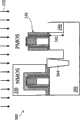
请参考图2A至图2C,其显示依据图1的方法50形成的本发明一实施例的结晶结构的工艺剖面图。在一实施例中,于例如硅的基板沟槽中生长一晶体。上述晶体可与基板相同或不同。在不同实施例中,上述晶体可包括硅、硅锗、锗、碳化硅或其他适合的半导体材料。在图2A中,提供一半导体基板102,其包括结晶结构的一硅基板或其他半导体基板,例如锗或三-五族化合物半导体。在另一实施例中,半导体基板102可包括一外延(epi)层。可利用蚀刻工艺或其他适合工艺于半导体基板102中形成一沟槽104。沟槽104可包括具有一结晶面方向(例如[100])的一底面106和具有一结晶面方向(例如[110]或[111])的一侧面108。值得注意的是,上述特定的结晶面方向仅做为实施例,然而也可使用其他的结晶面方向。Please refer to FIG. 2A to FIG. 2C , which show process cross-sectional views of a crystal structure according to an embodiment of the present invention formed according to the
在图2B中,可进行一由下而上生长工艺(bottom-up growth process)110,以于基板的沟槽104中生长一外延(epi)层。因此,上述下而上生长工艺可使用一或多个前驱物。在生长锗(Ge)外延层的实施例中,可使用气体流量介于5sccm至10sccm之间的GeH4和气体流量介于10sccm至30sccm之间的例如氯化氢(HCl)的蚀刻成分。在一些实施例中,蚀刻成分120可包括例如Cl2、BCl3、BiCl3或BiBr3的其他含氯气体或含溴气体。在其他实施例中,蚀刻成分120也可使用例如NF3或HF的含氟气体。然而,含氟气体可能会蚀刻浅沟槽隔绝氧化物和其他介电质(SiO2、SiN)硬掩模。于使外延(epi)层稳定生长的一温度下进行上述由下而上生长工艺110。在生长锗(Ge)外延层的实施例中,工艺温度可约介于450℃至550℃之间,且气体总压力介于20托尔(torr)至760托尔(torr)之间。应注意的是,例如氯化氢(HCl)的蚀刻成分对温度敏感且因此可调整温度以达成下述的想要的蚀刻效应。另外,可以了解的是,对不同类型的晶体材料的实施例可使用不同的条件范围。In FIG. 2B, a bottom-up
由于例如硅的基板102的不同的结晶面方向,所以底面106的生长速率不同于侧面108的生长速率。在一实施例中,可以得知锗在[100]结晶面方向(底面106)上的生长速度比在[110]结晶面方向(侧面108)上的生长速度快三倍。另外,可预期锗在[111]结晶面方向上的生长速度比比在[110]结晶面方向上的生长速度慢。因此,包含蚀刻成分120的由下而上生长工艺110可通过防止锗于沟槽104的侧面108生长,以促进锗由下而上生长。举例来说,锗从沟槽104的底面106的生长速度高于从沟槽104的侧面108的生长速度。蚀刻成分120同时移除沉积于侧面108和底面106的锗。然而,因为锗从沟槽104的底面106的生长速度大于从沟槽104的侧面108的生长速度,所以净效应为锗会大体上由下而上生长。The growth rate of the
在图2C中,持续进行由下而上生长工艺110直到外延层到达想要的厚度为止。值得注意的是,如果大体上基板和外延层之间的晶格不匹配程度大时,在底部会有一些错位缺陷。因此,因为基板和外延层之间的晶格不匹配,在沟槽的底部130的外延层结晶的一部分会包括错位缺陷。在硅沟槽中生长锗为一常见的实施例。然而,在一些其他实施例中,当基板和外延层之间的晶格不匹配程度小时,例如在锗沟槽中生长砷化锗,在底部不会有错位缺陷。In FIG. 2C , the bottom-up
另外,位于像锗结晶的具有晶格不匹配程度大的外延层之处的底部130上方的上部140,其大体上没有错位缺陷。此外,可以了解的是,因为通过蚀刻成分120禁止晶格不匹配程度大的外延层于侧面生长,所以侧面108不会表现出错位缺陷。因此,由下而上生长工艺110会捕捉错位缺陷,如果沟槽的底部130有任何的错位缺陷的话,且可在例如硅沟槽的基板上部140形成例如锗结构的一大体上无错位缺陷的纯单晶体。因此,因为锗结晶的无缺陷外延层具有比基板或晶体管沟道大或小的晶格常数,上述基板或晶体管沟道具有或不具有一理想的压缩或拉伸应力,所以像锗结晶的无缺陷外延层可用做为基板102中的一压缩或拉伸应力的压力源。In addition, the upper portion 140 above the bottom 130 where the epitaxial layer has a large lattice mismatch like a germanium crystal is substantially free of dislocation defects. In addition, it can be appreciated that the
虽然上述使用的纯锗晶体仅为一实施例,也可应用由下而上生长工艺来生长其他类型晶体结构,例如用于N型金属氧化物半导体晶体管(NMOS)元件压力源的碳化硅(SiC)、或可于硅或锗沟槽中生长例如砷化镓(GaAs)或锑化铟(InSb)的三-五族化合物半导体以做为沟道材料。就生长碳化硅(SiC)而言,蚀刻成分可相同于用于生长锗的蚀刻成分。就生长三-五族化合物半导体而言,蚀刻成分可包括包括含氯气体或含溴气体。Although the pure germanium crystal used above is only an example, other types of crystal structures can also be grown by applying bottom-up growth processes, such as silicon carbide (SiC) for N-type metal oxide semiconductor transistor (NMOS) device stressors. ), or a group III-V compound semiconductor such as gallium arsenide (GaAs) or indium antimonide (InSb) can be grown in a silicon or germanium trench as a channel material. For growing silicon carbide (SiC), the etch composition may be the same as that used to grow germanium. For growing Group III-V compound semiconductors, the etching composition may include a chlorine-containing gas or a bromine-containing gas.
另外,可以了解的是,可调整其他工艺参数以调整于不同结晶面上的生长速率。举例来说,温度、压力、蚀刻气体流量、乘载气体流量、沉积气体流量或上述组合可用以调整生长速率。此外,由下而上生长工艺可与例如互补式金属氧化物半导体晶体管(CMOS)的现行工艺完全相容且可易于与例如互补式金属氧化物半导体晶体管(CMOS)的现行工艺结合。Additionally, it can be appreciated that other process parameters can be adjusted to adjust growth rates on different crystallographic planes. For example, temperature, pressure, etchant gas flow, carrier gas flow, deposition gas flow, or combinations thereof may be used to adjust the growth rate. Furthermore, the bottom-up growth process is fully compatible with and can be easily combined with existing processes such as CMOS.
请参考图3,其显示依据本发明不同实施例的制造半导体装置的方法200的流程图。方法200起始于步骤202,提供一半导体基板。接着进行方法200的步骤204,于上述半导体基板上形成一栅极结构。接着进行方法200的步骤206,分别于上述栅极结构的侧壁上形成间隙壁。接着进行方法200的步骤208,于上述栅极结构的每一侧的基板中形成一凹陷。接着进行方法200的步骤210,利用由下而上生长工艺和蚀刻成分,外延生长一半导体材料以填充上述凹陷。接着进行方法200的步骤212,半导体装置制造完成。后续描述显示依据图3的方法200制造本发明不同实施例的半导体装置。Please refer to FIG. 3 , which shows a flowchart of a
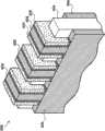
图4A至图4F为依据图3的半导体装置的制造方法200形成的本发明一实施例的半导体装置300的工艺剖面图。可以了解的是,为了清楚且易于了解本实施例的发明概念,简化图4A至图4F。在图4A中,半导体装置300可包括一基板302。基板302可包括一硅基板。在另一实施例中,基板302可包括一外延层。举例来说,基板302可包括位于一块状半导体上的一外延层。基板302可更包括例如p型井或n型井的掺杂区。此外,基板302可包括例如一埋藏介电层的绝缘层上覆硅(SOI)结构。在其他实施例中,基板302可包括例如埋藏一氧化层(BOX)的埋藏介电层,其可利用包括例如氧注入隔离法(SIMOX)、晶片接合(wafer bonding)、选择外延生长法(SEG)或其他适当方法的一方法形成。半导体装置300可包括定义于基板302中的有源区。4A to 4F are process cross-sectional views of a
为了隔绝不同的有源区,可于半导体基板中形成多个浅沟槽隔绝结构(STI)304。形成上述浅沟槽隔绝结构(STI)304的方式包括于基板中蚀刻一沟槽,利用例如氧化硅、氮化硅或氮氧化硅的绝缘材料填充上述沟槽。填充后的上述沟槽可为例如一热氧化衬垫层和填充沟槽的氮化硅的一多层结构。在一实施例中,可利用一工艺依序形成浅沟槽隔绝结构(STI)304,例如:生长一垫氧化物、形成一低压化学气相沉积(LPCVD)氮化层、利用光致抗蚀剂和掩模图案化一浅沟槽隔绝结构开口、于基板中蚀刻一沟槽、选择性生长一热氧化沟槽衬垫物以改善沟槽的介面、利用化学气相沉积(CVD)氧化物填充上述沟槽、利用化学机械研磨平坦化工艺以回蚀刻上述化学气相沉积(CVD)氧化物,且利用氮化物剥除法(nitride stripping)以留下浅沟槽隔绝结构(STI)。In order to isolate different active regions, a plurality of shallow trench isolation structures (STI) 304 may be formed in the semiconductor substrate. The method of forming the shallow trench isolation (STI) 304 includes etching a trench in the substrate, and filling the trench with an insulating material such as silicon oxide, silicon nitride or silicon oxynitride. The filled trench may be, for example, a multilayer structure of a thermal oxide liner layer and silicon nitride filling the trench. In one embodiment, the shallow trench isolation (STI) 304 may be sequentially formed using a process, such as: growing a pad oxide, forming a low pressure chemical vapor deposition (LPCVD) nitride layer, using photoresist patterning a shallow trench isolation structure opening with a mask, etching a trench in a substrate, selectively growing a thermally oxidized trench liner to improve the trench interface, filling the above with chemical vapor deposition (CVD) oxide The trenches are planarized using CMP to etch back the CVD oxide, and nitride stripping is used to leave shallow trench isolation (STI).
可于有源区中形成一个或多个操作元件。上述操作元件可包括n型和p型金属氧化物半导体场效应晶体管(以下简称为NMOS和PMOS元件)。可由NMOS和PMOS元件构成上述操作元件。可利用CMOS工艺形成上述NMOS和PMOS元件。另外,可以了解的是,可于图3的方法200之前、之中或之后提供额外的步骤,且可仅于说明书中简洁地描述其他工艺。每一个NMOS和PMOS元件可包括形成于半导体基板302上的一栅极结构。上述栅极结构可包括一栅极介电质306和一栅极308。上述栅极介电质306可包括氧化硅、氮化硅、高介电常数(high k)介电材料或其他适合的材料。上述高介电常数介电层可包括例如HfOx的二元或三元高介常数材料薄膜。在其他实施例中,上述高介电常数介电层可选择性包括例如LaO、AlO、ZrO、TiO、Ta2O5、Y2O3、SrTiO3(STO)、BaTiO3(BTO)、BaZrO、HfZrO、HfLaO、HfSiO、LaSiO、AlSiO、HfTaO、HfTiO、(Ba,Sr)TiO3(BST)、Al2O3、Si3N4、氮氧化硅或其他适当材料的其他高介电常数介电材料。可利用原子层沉积(ALD)法、化学气相沉积(CVD)法、物理气相沉积(PVD)法、热氧化法、紫外线臭氧氧化法或上述方式组合形成上述栅极介电质。One or more operational elements may be formed in the active region. The aforementioned operating elements may include n-type and p-type metal-oxide-semiconductor field-effect transistors (hereinafter referred to as NMOS and PMOS elements for short). The above-mentioned operation elements can be constituted by NMOS and PMOS elements. The above-mentioned NMOS and PMOS elements can be formed using a CMOS process. In addition, it is understood that additional steps may be provided before, during, or after the
上述栅极308可包括多晶硅层。举例来说,可使用硅烷(SiH4)做为化学气相沉积(CVD)工艺中一化学气体,以形成多晶硅层。上述多晶硅层的厚度可介于


半导体装置300可包括形成于栅极结构的每一个侧面上的偏移间隙壁(offset spacer)312。上述偏移间隙壁312可包括氮化硅或氮化硅。可利用化学气相沉积(CVD)法、物理气相沉积(PVD)法、原子层沉积(ALD)法、等离子体增强型化学气相沉积(PECVD)法或其他适合工艺形成上述偏移间隙壁312。可进行一注入工艺以于基板302中形成轻掺杂源/漏极(LDD)区(图未显示)。对PMOS元件而言,上述注入工艺可使用p型掺质(例如硼或铟),且对NMOS元件而言,上述注入工艺可使用n型掺质(例如磷或砷)。The
半导体装置300可更包括形成于基板302和栅极结构上方的一氧化层314。可利用化学气相沉积(CVD)法、原子层沉积(ALD)法、物理气相沉积(PVD)法或其他适合工艺形成上述氧化层314。氧化层314的厚度可介于2nm至2nm之间。半导体装置300可更包括形成氧化层314上方的氮化层316。可利用化学气相沉积(CVD)法、原子层沉积(ALD)法、物理气相沉积(PVD)法或其他适合工艺形成上述氮化层316。氮化层316的厚度可介于10nm至15nm之间。可蚀刻氧化层314和氮化层316以形成间隙壁,其用以形成如下所述的源极和漏极应力物。因此,氧化层314和氮化层316的厚度取决于源极和漏极应力物与PMOS元件的一沟道区相隔的距离。The
形成一图案化光致抗蚀剂层320以保护NMOS元件。一实施例的光刻工艺可包括光致抗蚀剂涂布、软烤、掩模对准、曝光、曝光后烘烤、光致抗蚀剂显影和硬烤的工艺步骤。可更利用其他适合工艺进行上述光刻曝光工艺或以其他适合工艺取代上述光刻曝光工艺,上述其他适合工艺例如为无光掩模光刻工艺、电子束写入工艺、离子束写入工艺或分子拓印工艺(molecularimprint)。A patterned
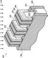
在图4B中,可进行一蚀刻工艺324,以移除位于基板302正上方的部分氮化层316。在本实施例中,蚀刻工艺324可包括使用CHxFy/O2 orSF6/CHxFy/He(其中x=1至3,且y=4-x)的一气体组合或其他气体组合的一干蚀刻工艺。上述干蚀刻工艺提供方向性蚀刻(例如异向性蚀刻),以使氮化层316a的一些部分在进行蚀刻工艺324之后残留于栅极结构的侧壁上。In FIG. 4B , an
在图4C中,进行一蚀刻工艺328,以移除位于基板302正上方的氧化层314。在本实施例中,蚀刻工艺328可包括使用CF4/Cl2/HBr/He的一气体组合或其他气体组合的一干蚀刻工艺。因此,进行蚀刻工艺328之后,残留于PMOS元件的栅极结构的侧壁上的一部分氧化层314a氮化层316a因而形成间隙壁330。In FIG. 4C , an
在图4D中,进行一蚀刻工艺332,以于基板302中蚀刻一凹陷340。蚀刻工艺332可包括使用HBr/Cl2/O2/He的一气体组合的一干蚀刻工艺,且气体压力可约介于1mT至1000mT之间,功率可介于50W至1000W之间,偏压介于100V至500V之间,且HBr的气体流量可介于10sccm至500sccm之间,Cl2的气体流量可介于0sccm至500sccm之间,O2的气体流量可介于0sccm至100sccm之间,且He的气体流量可介于0sccm至1000sccm之间。上述干蚀刻工艺移除未被保护或暴露出来的一部分基板302。因为方向性蚀刻/异向性蚀刻,因此凹陷340具有垂直的侧壁且对齐于间隙壁330。上述凹陷340可具有一深度342,其可介于

在图4E中,进行一外延工艺350,以于凹陷340中沉积一半导体材料。于进行外延工艺350之前移除保护NMOS元件的图案化光致抗蚀剂层320。可使用氢氟酸(HF)或其他适当溶液进行一预清洁工艺,以清洁凹陷340。在本实施例中,外延工艺350类似于如图2A至图2C所述的由下而上生长工艺110。因此,于凹陷340中生长一纯锗结晶结构355,以形成源极和漏极应力物。可以了解的是,有一些错位缺陷会被纯锗结晶结构355的底部357,然而这些错位缺陷应该不会反过来影响PMOS元件的性能。另外,在一些实施例中,可沉积纯锗结晶结构355,以使其凸起于基板302的表面一距离。In FIG. 4E , an epitaxial process 350 is performed to deposit a semiconductor material in the
如前所述,用于源极和漏极应力物的现行硅锗结构被其可产生应力的数量限制。硅锗结构中的锗浓度决定可产生应力的数量,且因此增加上述锗浓度将会增加应力的大小。然而,只能增加上述锗浓度到一定程度,以达到应力硅锗结构的足够结晶厚度。在此,在本实施例中,可形成无缺陷的纯锗结晶结构,以做为源极和漏极应力物或高迁移率沟道。就其本身而论,纯锗结晶结构355会产生一明显数量的压缩应力(例如4GPa或大于4GPa)359,以增强空穴迁移率且改善位于硅或硅锗基板上的PMOS元件性能。因此,因为锗源极和漏极应力物本身会提供大于4GPa的压缩沟道应力以达到最大的硅空穴迁移率,所以不再需要例如接触蚀刻停止层(CESL)的其他类型应力物。在本实施例中,外延工艺350可以原位掺杂(in-situ doped)锗和例如硼或铟的p型掺质,以形成PMOS元件的源极和漏极区。As previously mentioned, current SiGe structures for source and drain stressors are limited by the amount of stress they can generate. The germanium concentration in the SiGe structure determines the amount of stress that can be induced, and thus increasing the germanium concentration will increase the amount of stress. However, the above-mentioned germanium concentration can only be increased to a certain extent in order to achieve a sufficient crystalline thickness of the stressed SiGe structure. Here, in this embodiment, a defect-free pure Ge crystalline structure can be formed to serve as source and drain stressors or high mobility channels. As such, the pure germanium
在图4F中,进行一蚀刻工艺360,以移除NMOS元件上的氮化层316和PMOS元件上的氮化层316a。上述蚀刻工艺360包含用磷酸(H3PO4)或其他适当蚀刻剂的湿蚀刻工艺。可选择上述湿蚀刻工艺,以达到慢的蚀刻速率,以保护多晶硅。接着进行以下简述工艺以完成半导体装置300的制造方法。举例来说,利用例如磷或砷的n型离子注入工艺以形成NMOS元件的源/漏极区。在另一实施例中,可利用上述由下而上生长工艺,于硅基板沟槽中沉积碳化硅(SiC),以形成NMOS元件的源/漏极区。另外,可于凸起的源/漏极物上形成硅化物,以降低接触电阻。可利用包括沉积一金属层、将上述金属层退火使能够与硅反应以形成硅化物且移除未反应的金属层的一工艺,于源/漏极上形成硅化物。In FIG. 4F, an
可于基板上形成一层间介电质(ILD),再对基板进行一化学机械研磨(CMP)工艺以平坦化基板。在一实施例中,在最终装置中,栅极308残留有多晶硅。在另一实施例中,在栅极后置工艺(gate last process)或栅极取代工艺(gate replacement process)中,移除多晶硅且以一金属取代在栅极后置工艺(gate last process)中,持续层间介电层(ILD layer)上的化学机械研磨(CMP)工艺直到暴露出多晶硅表面,且进行一蚀刻工艺以移除多晶硅因而形成沟槽。以一适当功函数材料(例如p型功函数材料或n型功函数材料)上述填充在PMOS和NMOS元件中的上述沟槽。于基板上形成一多层内连线(MLI)以电性连接不同元件以形成一集成电路。上述多层内连线(MLI)包括例如常用的介层孔或接触插塞的垂直内连线,和例如金属线的水平内连线。可用包括铜、钨和硅化物的各种导电材料形成上述各种内连线。在一实施例中,可使用镶嵌工艺以形成铜内连线结构。An interlayer dielectric (ILD) may be formed on the substrate, and then a chemical mechanical polishing (CMP) process is performed on the substrate to planarize the substrate. In one embodiment, the
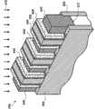
请参考图5A至图5D,其为本发明另一实施例的半导体装置400的工艺剖面图。半导体装置400包括鳍状场效应晶体管(FinFET)元件。可以了解的是,为了清楚且更了解本实施例的发明概念,简化图5A至图5D,且一些常用的元件和工艺在此不做叙述。在图5A中,半导体装置400可包括一基板(图未显示)。基板可包括结晶硅。半导体装置400可包括从基板延伸的多个鳍状物404。虽然附图中只显示一个鳍状物,但可以了解的是,可依特定实施例改变鳍状物的数量。鳍状物404可包括硅。可利用例如光刻工艺和蚀刻工艺的适当工艺形成鳍状物404。举例来说,上述光刻工艺可包括于基板上形成一光致抗蚀剂层、将上述光致抗蚀剂层曝光以成为一图案、进行曝光后烘烤工艺、且将光致抗蚀剂显影以形成包括光致抗蚀剂的一掩模元件。然后使用上述掩模元件以从上述基板蚀刻上述鳍状物404。可利用反应式离子蚀刻法(RIE)及/或其他适当工艺蚀刻上述鳍状物404。浅沟槽隔绝(STI)结构406围绕上述鳍状物404且将每一个鳍状物与其他鳍状物彼此隔绝。浅沟槽隔绝(STI)结构406可包括任何适当绝缘材料。Please refer to FIG. 5A to FIG. 5D , which are process cross-sectional views of a
在其他实施例中,基板可包括一绝缘层上覆硅(SOI)基板。可利用氧注入隔离法(SIMOX)、晶片接合(wafer bonding)及/或其他适当工艺形成上述绝缘层上覆硅(SOI)基板。硅层可包括一绝缘层上覆硅(SOI)基板上的一硅层(例如位于一绝缘层上)。举例来说,可利用蚀刻基板上的一硅层形成上述鳍状物。In other embodiments, the substrate may include a silicon-on-insulator (SOI) substrate. The silicon-on-insulator (SOI) substrate described above may be formed by isolation by implantation of oxygen (SIMOX), wafer bonding, and/or other suitable processes. The silicon layer may include a silicon layer on a silicon-on-insulator (SOI) substrate (eg, on an insulating layer). For example, the fins may be formed by etching a silicon layer on the substrate.
半导体装置400包括形成于部分上述鳍状物404上方的多重栅极结构408。栅极结构408包覆环绕上述鳍状物404,以允许形成于上述鳍状物两侧边的沟道的栅极控制。栅极结构408可包括类似于图4A所述的一栅极介电质、一栅极和一硬掩模。可于栅极结构408的侧壁上形成间隙壁409。The
在图5B中,进行一蚀刻工艺410,以移除鳍状物404的暴露部分。在本实施例中,蚀刻工艺410类似于图4D所述的蚀刻工艺332。因此,进行蚀刻工艺410之后,形成一凹陷420。凹陷420可具有具有一第一结晶面方向(例如[100])的一底面422,和具有一第二结晶面方向(例如[110])的一侧面424。可以了解的是,浅沟槽隔绝(STI)结构406形成于凹陷420的其他侧面。In FIG. 5B , an
在图5C中,进行一外延工艺430,以于凹陷420中沉积一半导体材料。在本实施例中,外延工艺430类似于图2A至图2C所述的由下而上生长工艺110。锗在第一结晶面方向(底面422)上的生长速度大于在第二结晶面方向(侧面424)上的生长速度。如上所述,在外延工艺430期间,蚀刻成分控制和禁止侧面424上的生长。此外,蚀刻成分可移除可能沉积于浅沟槽隔绝(STI)结构406侧面的锗。因此,于凹陷420中大体上由下而上生长一纯锗结晶结构440。持续由下而上生长工艺往上生长至浅沟槽隔绝(STI)结构406的表面。在图5D中,持续由下而上生长工艺至超过浅沟槽隔绝(STI)结构406的表面,且完成形成具有一理想高度的纯锗结晶结构440。锗源极和漏极应力物的纯锗结晶结构440增强空穴迁移率,上述空穴迁移率改善元件性能。In FIG. 5C , an
虽然本发明已以实施例公开如上,然其并非用以限定本发明,任何本领域普通技术人员,在不脱离本发明的精神和范围内,当可作些许的更动与润饰,因此本发明的保护范围当视随附的权利要求所界定的保护范围为准。Although the present invention has been disclosed as above with the embodiments, it is not intended to limit the present invention. Anyone skilled in the art can make some changes and modifications without departing from the spirit and scope of the present invention. Therefore, the present invention The scope of protection should be subject to the scope of protection defined by the appended claims.
Claims (6)
Applications Claiming Priority (4)
| Application Number | Priority Date | Filing Date | Title |
|---|---|---|---|
| US25643109P | 2009-10-30 | 2009-10-30 | |
| US61/256,431 | 2009-10-30 | ||
| US12/784,207US8415718B2 (en) | 2009-10-30 | 2010-05-20 | Method of forming epi film in substrate trench |
| US12/784,207 | 2010-05-20 |
Publications (2)
| Publication Number | Publication Date |
|---|---|
| CN102074461A CN102074461A (en) | 2011-05-25 |
| CN102074461Btrue CN102074461B (en) | 2014-03-05 |
Family
ID=43924453
Family Applications (1)
| Application Number | Title | Priority Date | Filing Date |
|---|---|---|---|
| CN201010518047.9AActiveCN102074461B (en) | 2009-10-30 | 2010-10-20 | Semiconductor device and manufacturing method thereof |
Country Status (3)
| Country | Link |
|---|---|
| US (3) | US8415718B2 (en) |
| CN (1) | CN102074461B (en) |
| TW (1) | TWI424474B (en) |
Families Citing this family (137)
| Publication number | Priority date | Publication date | Assignee | Title |
|---|---|---|---|---|
| US8153493B2 (en) | 2008-08-28 | 2012-04-10 | Taiwan Semiconductor Manufacturing Company, Ltd. | FinFET process compatible native transistor |
| EP2335273A4 (en)* | 2008-09-19 | 2012-01-25 | Taiwan Semiconductor Mfg | FORMATION OF DEVICES BY GROWTH OF EPITAXIAL LAYERS |
| US8357569B2 (en) | 2009-09-29 | 2013-01-22 | Taiwan Semiconductor Manufacturing Company, Ltd. | Method of fabricating finfet device |
| US8110466B2 (en) | 2009-10-27 | 2012-02-07 | Taiwan Semiconductor Manufacturing Company, Ltd. | Cross OD FinFET patterning |
| US8310013B2 (en) | 2010-02-11 | 2012-11-13 | Taiwan Semiconductor Manufacturing Company, Ltd. | Method of fabricating a FinFET device |
| US8942030B2 (en) | 2010-06-25 | 2015-01-27 | Taiwan Semiconductor Manufacturing Company, Ltd. | Structure and method for SRAM cell circuit |
| US8212295B2 (en) | 2010-06-30 | 2012-07-03 | Taiwan Semiconductor Manufacturing Company, Ltd. | ROM cell circuit for FinFET devices |
| US8796759B2 (en) | 2010-07-15 | 2014-08-05 | Taiwan Semiconductor Manufacturing Company, Ltd. | Fin-like field effect transistor (FinFET) device and method of manufacturing same |
| US9130058B2 (en) | 2010-07-26 | 2015-09-08 | Taiwan Semiconductor Manufacturing Company, Ltd. | Forming crown active regions for FinFETs |
| US8062963B1 (en) | 2010-10-08 | 2011-11-22 | Taiwan Semiconductor Manufacturing Company, Ltd. | Method of fabricating a semiconductor device having an epitaxy region |
| US8367498B2 (en) | 2010-10-18 | 2013-02-05 | Taiwan Semiconductor Manufacturing Company, Ltd. | Fin-like field effect transistor (FinFET) device and method of manufacturing same |
| US9472550B2 (en) | 2010-11-23 | 2016-10-18 | Taiwan Semiconductor Manufacturing Company, Ltd. | Adjusted fin width in integrated circuitry |
| US8633076B2 (en) | 2010-11-23 | 2014-01-21 | Taiwan Semiconductor Manufacturing Company, Ltd. | Method for adjusting fin width in integrated circuitry |
| US8796124B2 (en) | 2011-10-25 | 2014-08-05 | Taiwan Semiconductor Manufacturing Company, Ltd. | Doping method in 3D semiconductor device |
| JP5541265B2 (en)* | 2011-11-18 | 2014-07-09 | 信越化学工業株式会社 | Etching mask film evaluation method |
| US8741726B2 (en)* | 2011-12-01 | 2014-06-03 | Taiwan Semiconductor Manufacturing Company, Ltd. | Reacted layer for improving thickness uniformity of strained structures |
| KR101700213B1 (en) | 2011-12-21 | 2017-01-26 | 인텔 코포레이션 | Methods for forming fins for metal oxide semiconductor device structures |
| US8486770B1 (en) | 2011-12-30 | 2013-07-16 | Taiwan Semiconductor Manufacturing Company, Ltd. | Method of forming CMOS FinFET device |
| US8822106B2 (en)* | 2012-04-13 | 2014-09-02 | Taiwan Semiconductor Manufacturing Company, Ltd. | Grid refinement method |
| JP6207170B2 (en) | 2012-02-15 | 2017-10-04 | アイメックImec | Mask structure and method for defect-free heteroepitaxial |
| US9012286B2 (en) | 2012-04-12 | 2015-04-21 | Globalfoundries Inc. | Methods of forming FinFET semiconductor devices so as to tune the threshold voltage of such devices |
| US9190471B2 (en) | 2012-04-13 | 2015-11-17 | Globalfoundries U.S.2 Llc | Semiconductor structure having a source and a drain with reverse facets |
| US8580642B1 (en) | 2012-05-21 | 2013-11-12 | Globalfoundries Inc. | Methods of forming FinFET devices with alternative channel materials |
| US8889501B2 (en)* | 2012-06-01 | 2014-11-18 | Taiwan Semiconductor Manufacturing Company, Ltd. | Methods for forming MOS devices with raised source/drain regions |
| US8673718B2 (en) | 2012-07-09 | 2014-03-18 | Globalfoundries Inc. | Methods of forming FinFET devices with alternative channel materials |
| US9142400B1 (en) | 2012-07-17 | 2015-09-22 | Stc.Unm | Method of making a heteroepitaxial layer on a seed area |
| CN103779215B (en)* | 2012-10-18 | 2016-09-21 | 中芯国际集成电路制造(上海)有限公司 | A kind of semiconductor device and preparation method thereof |
| US8866235B2 (en)* | 2012-11-09 | 2014-10-21 | Taiwan Semiconductor Manufacturing Company, Ltd. | Source and drain dislocation fabrication in FinFETs |
| US8809139B2 (en) | 2012-11-29 | 2014-08-19 | Taiwan Semiconductor Manufacturing Company, Ltd. | Fin-last FinFET and methods of forming same |
| US8815659B2 (en) | 2012-12-17 | 2014-08-26 | Globalfoundries Inc. | Methods of forming a FinFET semiconductor device by performing an epitaxial growth process |
| US8765546B1 (en)* | 2013-06-24 | 2014-07-01 | United Microelectronics Corp. | Method for fabricating fin-shaped field-effect transistor |
| CN105308719B (en) | 2013-06-28 | 2019-07-26 | 英特尔公司 | Device based on selective epitaxial growth of III-V materials |
| CN105531797A (en)* | 2013-06-28 | 2016-04-27 | 英特尔公司 | Nanostructures and nanofeatures with Si(111) planes on Si(100) wafers for III-N epitaxy |
| KR102089682B1 (en)* | 2013-07-15 | 2020-03-16 | 삼성전자 주식회사 | Semiconductor device and method for fabricating the same |
| US9553012B2 (en) | 2013-09-13 | 2017-01-24 | Taiwan Semiconductor Manufacturing Company Ltd. | Semiconductor structure and the manufacturing method thereof |
| US9064699B2 (en) | 2013-09-30 | 2015-06-23 | Samsung Electronics Co., Ltd. | Methods of forming semiconductor patterns including reduced dislocation defects and devices formed using such methods |
| US9406547B2 (en)* | 2013-12-24 | 2016-08-02 | Intel Corporation | Techniques for trench isolation using flowable dielectric materials |
| US9548303B2 (en) | 2014-03-13 | 2017-01-17 | Taiwan Semiconductor Manufacturing Company, Ltd. | FinFET devices with unique fin shape and the fabrication thereof |
| US9343303B2 (en) | 2014-03-20 | 2016-05-17 | Samsung Electronics Co., Ltd. | Methods of forming low-defect strain-relaxed layers on lattice-mismatched substrates and related semiconductor structures and devices |
| US9853107B2 (en) | 2014-03-28 | 2017-12-26 | Intel Corporation | Selective epitaxially grown III-V materials based devices |
| US9887100B2 (en)* | 2014-10-03 | 2018-02-06 | Taiwan Semiconductor Manufacturing Company, Ltd. | Methods of forming semiconductor devices and structures thereof |
| US9852902B2 (en) | 2014-10-03 | 2017-12-26 | Applied Materials, Inc. | Material deposition for high aspect ratio structures |
| KR102255174B1 (en) | 2014-10-10 | 2021-05-24 | 삼성전자주식회사 | Semiconductor device having active region and method of forming the same |
| CN105633152B (en) | 2014-11-05 | 2019-12-10 | 联华电子股份有限公司 | Semiconductor structure and manufacturing method thereof |
| US9349809B1 (en)* | 2014-11-14 | 2016-05-24 | International Business Machines Corporation | Aspect ratio trapping and lattice engineering for III/V semiconductors |
| CN104409409A (en)* | 2014-11-19 | 2015-03-11 | 上海华力微电子有限公司 | Method for improving SiC stress property of shallow trench isolation edge |
| US9391201B2 (en) | 2014-11-25 | 2016-07-12 | Taiwan Semiconductor Manufacturing Company, Ltd. | Source/drain structure and manufacturing the same |
| CN104393050A (en)* | 2014-11-26 | 2015-03-04 | 上海华力微电子有限公司 | Method for improving performance of STI (Shallow Trench Isolation) edge epitaxial layer and corresponding semiconductor structure thereof |
| US9269628B1 (en) | 2014-12-04 | 2016-02-23 | Globalfoundries Inc. | Methods of removing portions of at least one fin structure so as to form isolation regions when forming FinFET semiconductor devices |
| US9349652B1 (en) | 2014-12-12 | 2016-05-24 | Taiwan Semiconductor Manufacturing Company, Ltd. | Method of forming semiconductor device with different threshold voltages |
| CN105762106B (en) | 2014-12-18 | 2021-02-19 | 联华电子股份有限公司 | Semiconductor device and manufacturing process thereof |
| US9780214B2 (en) | 2014-12-22 | 2017-10-03 | Taiwan Semiconductor Manufacturing Co., Ltd. | Semiconductor device including Fin- FET and manufacturing method thereof |
| US9768301B2 (en) | 2014-12-23 | 2017-09-19 | Taiwan Semiconductor Manufacturing Company, Ltd. | Short channel effect suppression |
| US10134871B2 (en) | 2014-12-23 | 2018-11-20 | Taiwan Semiconductor Manufacturing Company, Ltd. | Doping of high-K dielectric oxide by wet chemical treatment |
| US10141310B2 (en) | 2014-12-23 | 2018-11-27 | Taiwan Semiconductor Manufacturing Company, Ltd. | Short channel effect suppression |
| US9515071B2 (en) | 2014-12-24 | 2016-12-06 | Taiwan Semiconductor Manufacturing Company, Ltd. | Asymmetric source/drain depths |
| US9425250B2 (en) | 2014-12-30 | 2016-08-23 | Taiwan Semiconductor Manufacturing Company, Ltd. | Transistor with wurtzite channel |
| US9647090B2 (en) | 2014-12-30 | 2017-05-09 | Taiwan Semiconductor Manufacturing Company, Ltd. | Surface passivation for germanium-based semiconductor structure |
| US9601626B2 (en) | 2015-01-23 | 2017-03-21 | Taiwan Semiconductor Manufacturing Co., Ltd. | Semiconductor device including fin structure with two channel layers and manufacturing method thereof |
| TWI629790B (en)* | 2015-01-26 | 2018-07-11 | 聯華電子股份有限公司 | Semiconductor component and manufacturing method thereof |
| US9379182B1 (en) | 2015-02-03 | 2016-06-28 | United Microelectronics Corp. | Method for forming nanowire and semiconductor device formed with the nanowire |
| US9443729B1 (en) | 2015-03-31 | 2016-09-13 | Taiwan Semiconductor Manufacturing Company, Ltd. | Method for forming FinFET devices |
| US9590102B2 (en) | 2015-04-15 | 2017-03-07 | Taiwan Semiconductor Manufacturing Co., Ltd. | Semiconductor device and manufacturing method thereof |
| US9680014B2 (en) | 2015-04-17 | 2017-06-13 | Taiwan Semiconductor Manufacturing Co., Ltd. | Semiconductor device including Fin structures and manufacturing method thereof |
| US9570557B2 (en) | 2015-04-29 | 2017-02-14 | Taiwan Semiconductor Manufacturing Co., Ltd. | Tilt implantation for STI formation in FinFET structures |
| US9773786B2 (en) | 2015-04-30 | 2017-09-26 | Taiwan Semiconductor Manufacturing Company, Ltd. | FETs and methods of forming FETs |
| US9461110B1 (en) | 2015-04-30 | 2016-10-04 | Taiwan Semiconductor Manufacturing Company, Ltd. | FETs and methods of forming FETs |
| TWI642184B (en) | 2015-05-15 | 2018-11-21 | 聯華電子股份有限公司 | Non-planar transistor and manufacturing method thereof |
| US10269968B2 (en) | 2015-06-03 | 2019-04-23 | Taiwan Semiconductor Manufacturing Co., Ltd. | Semiconductor device including fin structures and manufacturing method thereof |
| US9449975B1 (en) | 2015-06-15 | 2016-09-20 | Taiwan Semiconductor Manufacturing Company, Ltd. | FinFET devices and methods of forming |
| US9647071B2 (en) | 2015-06-15 | 2017-05-09 | Taiwan Semiconductor Manufacturing Company, Ltd. | FINFET structures and methods of forming the same |
| US9425313B1 (en) | 2015-07-07 | 2016-08-23 | Taiwan Semiconductor Manufacturing Co., Ltd. | Semiconductor device and manufacturing method thereof |
| US9953881B2 (en) | 2015-07-20 | 2018-04-24 | Taiwan Semiconductor Manufacturing Company, Ltd. | Method of forming a FinFET device |
| US9472620B1 (en) | 2015-09-04 | 2016-10-18 | Taiwan Semiconductor Manufacturing Co., Ltd. | Semiconductor device including fin structures and manufacturing method thereof |
| US9680017B2 (en) | 2015-09-16 | 2017-06-13 | Taiwan Semiconductor Manufacturing Co., Ltd. | Semiconductor device including Fin FET and manufacturing method thereof |
| US10121858B2 (en) | 2015-10-30 | 2018-11-06 | Taiwan Semiconductor Manufacturing Company, Ltd. | Elongated semiconductor structure planarization |
| US12165869B2 (en) | 2015-11-16 | 2024-12-10 | Taiwan Semiconductor Manufacturing Co., Ltd. | Transistors comprising a vertical stack of elongated semiconductor features |
| US10020304B2 (en)* | 2015-11-16 | 2018-07-10 | Taiwan Semiconductor Manufacturing Co., Ltd. | Fin field effect transistor, semiconductor device and fabricating method thereof |
| US10032627B2 (en) | 2015-11-16 | 2018-07-24 | Taiwan Semiconductor Manufacturing Company, Ltd. | Method for forming stacked nanowire transistors |
| US9960273B2 (en) | 2015-11-16 | 2018-05-01 | Taiwan Semiconductor Manufacturing Company, Ltd. | Integrated circuit structure with substrate isolation and un-doped channel |
| US9887269B2 (en) | 2015-11-30 | 2018-02-06 | Taiwan Semiconductor Manufacturing Company, Ltd. | Multi-gate device and method of fabrication thereof |
| US9564317B1 (en) | 2015-12-02 | 2017-02-07 | Taiwan Semiconductor Manufacturing Company, Ltd. | Method of forming a nanowire |
| US9570297B1 (en) | 2015-12-09 | 2017-02-14 | International Business Machines Corporation | Elimination of defects in long aspect ratio trapping trench structures |
| US9716146B2 (en) | 2015-12-15 | 2017-07-25 | Taiwan Semiconductor Manufacturing Company, Ltd. | Integrated circuit structure and method with solid phase diffusion |
| US9899269B2 (en) | 2015-12-30 | 2018-02-20 | Taiwan Semiconductor Manufacturing Company, Ltd | Multi-gate device and method of fabrication thereof |
| US9660033B1 (en) | 2016-01-13 | 2017-05-23 | Taiwan Semiconductor Manufactuing Company, Ltd. | Multi-gate device and method of fabrication thereof |
| US9876098B2 (en) | 2016-01-15 | 2018-01-23 | Taiwan Semiconductor Manufacturing Company, Ltd. | Method of forming a gate spacer |
| US10038095B2 (en) | 2016-01-28 | 2018-07-31 | Taiwan Semiconductor Manufacturing Co., Ltd. | V-shape recess profile for embedded source/drain epitaxy |
| US10453925B2 (en) | 2016-01-29 | 2019-10-22 | Taiwan Semiconductor Manufacturing Co., Ltd. | Epitaxial growth methods and structures thereof |
| US10340383B2 (en) | 2016-03-25 | 2019-07-02 | Taiwan Semiconductor Manufacturing Co., Ltd. | Semiconductor device having stressor layer |
| US11018254B2 (en)* | 2016-03-31 | 2021-05-25 | International Business Machines Corporation | Fabrication of vertical fin transistor with multiple threshold voltages |
| US10164061B2 (en) | 2016-05-19 | 2018-12-25 | Taiwan Semiconductor Manufacturing Co., Ltd. | Method of fabricating non-volatile memory device array |
| US10734522B2 (en) | 2016-06-15 | 2020-08-04 | Taiwan Semiconductor Manufacturing Co., Ltd. | Structure and formation method of semiconductor device structure with gate stacks |
| US10008414B2 (en) | 2016-06-28 | 2018-06-26 | Taiwan Semiconductor Manufacturing Co., Ltd. | System and method for widening Fin widths for small pitch FinFET devices |
| US9620628B1 (en) | 2016-07-07 | 2017-04-11 | Taiwan Semiconductor Manufacturing Co., Ltd. | Methods of forming contact feature |
| US10269938B2 (en) | 2016-07-15 | 2019-04-23 | Taiwan Semiconductor Manufacturing Co., Ltd. | Semiconductor device structure having a doped passivation layer |
| US10217741B2 (en) | 2016-08-03 | 2019-02-26 | Taiwan Semiconductor Manufacturing Company, Ltd. | Fin structure and method of forming same through two-step etching processes |
| US9853150B1 (en) | 2016-08-15 | 2017-12-26 | Taiwan Semiconductor Manufacturing Co., Ltd. | Method of fabricating epitaxial gate dielectrics and semiconductor device of the same |
| US9865589B1 (en) | 2016-10-31 | 2018-01-09 | Taiwan Semiconductor Manufacturing Co., Ltd. | System and method of fabricating ESD FinFET with improved metal landing in the drain |
| US11152362B2 (en) | 2016-11-10 | 2021-10-19 | Taiwan Semiconductor Manufacturing Co., Ltd. | Fin field effect transistor (FinFET) device structure |
| US9847334B1 (en) | 2016-11-18 | 2017-12-19 | Taiwan Semiconductor Manufacturing Co., Ltd. | Structure and formation method of semiconductor device with channel layer |
| US10879240B2 (en) | 2016-11-18 | 2020-12-29 | Taiwan Semiconductor Manufacturing Co., Ltd. | Fin field effect transistor (FinFET) device structure |
| KR20180061478A (en)* | 2016-11-28 | 2018-06-08 | 삼성전자주식회사 | Semiconductor device |
| US10134870B2 (en) | 2016-11-28 | 2018-11-20 | Taiwan Semiconductor Manufacturing Co., Ltd. | Semiconductor structure and method of manufacturing the same |
| US10290546B2 (en) | 2016-11-29 | 2019-05-14 | Taiwan Semiconductor Manufacturing Co., Ltd. | Threshold voltage adjustment for a gate-all-around semiconductor structure |
| US10062782B2 (en) | 2016-11-29 | 2018-08-28 | Taiwan Semiconductor Manufacturing Co., Ltd. | Method of manufacturing a semiconductor device with multilayered channel structure |
| US11011634B2 (en) | 2016-11-30 | 2021-05-18 | Taiwan Semiconductor Manufacturing Co., Ltd. | Elongated source/drain region structure in finFET device |
| US9865595B1 (en) | 2016-12-14 | 2018-01-09 | Taiwan Semiconductor Manufacturing Co., Ltd. | FinFET device with epitaxial structures that wrap around the fins and the method of fabricating the same |
| US9899273B1 (en) | 2016-12-15 | 2018-02-20 | Taiwan Semiconductor Manufacturing Co., Ltd. | Semiconductor structure with dopants diffuse protection and method for forming the same |
| US10522643B2 (en) | 2017-04-26 | 2019-12-31 | Taiwan Semiconductor Manufacturing Co., Ltd. | Device and method for tuning threshold voltage by implementing different work function metals in different segments of a gate |
| US10522417B2 (en) | 2017-04-27 | 2019-12-31 | Taiwan Semiconductor Manufacturing Co., Ltd. | FinFET device with different liners for PFET and NFET and method of fabricating thereof |
| US10453753B2 (en) | 2017-08-31 | 2019-10-22 | Taiwan Semiconductor Manufacturing Co., Ltd. | Using a metal-containing layer as an etching stop layer and to pattern source/drain regions of a FinFET |
| US10276697B1 (en) | 2017-10-27 | 2019-04-30 | Taiwan Semiconductor Manufacturing Co., Ltd. | Negative capacitance FET with improved reliability performance |
| US10522557B2 (en) | 2017-10-30 | 2019-12-31 | Taiwan Semiconductor Manufacturing Co., Ltd. | Surface topography by forming spacer-like components |
| US20190131454A1 (en)* | 2017-11-01 | 2019-05-02 | Qualcomm Incorporated | Semiconductor device with strained silicon layers on porous silicon |
| US10366915B2 (en) | 2017-11-15 | 2019-07-30 | Taiwan Semiconductor Manufacturing Co., Ltd. | FinFET devices with embedded air gaps and the fabrication thereof |
| US10510894B2 (en) | 2017-11-30 | 2019-12-17 | Taiwan Semiconductor Manufacturing Co., Ltd. | Isolation structure having different distances to adjacent FinFET devices |
| US10854615B2 (en) | 2018-03-30 | 2020-12-01 | Taiwan Semiconductor Manufacturing Co., Ltd. | FinFET having non-merging epitaxially grown source/drains |
| US10431502B1 (en) | 2018-04-16 | 2019-10-01 | International Business Machines Corporation | Maskless epitaxial growth of phosphorus-doped Si and boron-doped SiGe (Ge) for advanced source/drain contact |
| US10665697B2 (en) | 2018-06-15 | 2020-05-26 | Taiwan Semiconductor Manufacturing Company, Ltd. | Semiconductor device and method |
| US11043556B2 (en) | 2018-06-26 | 2021-06-22 | Taiwan Semiconductor Manufacturing Co., Ltd. | Local epitaxy nanofilms for nanowire stack GAA device |
| US11302535B2 (en) | 2018-06-27 | 2022-04-12 | Taiwan Semiconductor Manufacturing Co., Ltd. | Performing annealing process to improve fin quality of a FinFET semiconductor |
| US10388771B1 (en) | 2018-06-28 | 2019-08-20 | Taiwan Semiconductor Manufacturing Co., Ltd. | Method and device for forming cut-metal-gate feature |
| US10790352B2 (en) | 2018-06-28 | 2020-09-29 | Taiwan Semiconductor Manufacturing Co., Ltd. | High density capacitor implemented using FinFET |
| US10886226B2 (en) | 2018-07-31 | 2021-01-05 | Taiwan Semiconductor Manufacturing Co, Ltd. | Conductive contact having staircase barrier layers |
| DE102019118061A1 (en) | 2018-09-19 | 2020-03-19 | Taiwan Semiconductor Manufacturing Co., Ltd. | SELECTIVE DOUBLE SILICIDE MANUFACTURING USING A MASKLESS MANUFACTURING PROCESS |
| US10998241B2 (en) | 2018-09-19 | 2021-05-04 | Taiwan Semiconductor Manufacturing Co., Ltd. | Selective dual silicide formation using a maskless fabrication process flow |
| US10971605B2 (en) | 2018-10-22 | 2021-04-06 | Taiwan Semiconductor Manufacturing Co., Ltd. | Dummy dielectric fin design for parasitic capacitance reduction |
| US11728344B2 (en) | 2019-06-28 | 2023-08-15 | Taiwan Semiconductor Manufacturing Co., Ltd. | Hybrid SRAM design with nano-structures |
| US11165032B2 (en)* | 2019-09-05 | 2021-11-02 | Taiwan Semiconductor Manufacturing Co., Ltd. | Field effect transistor using carbon nanotubes |
| US11469238B2 (en) | 2019-09-26 | 2022-10-11 | Taiwan Semiconductor Manufacturing Co., Ltd. | Non-interleaving N-well and P-well pickup region design for IC devices |
| US11222952B2 (en)* | 2020-01-22 | 2022-01-11 | Qualcomm Incorporated | Gate all around transistors with high charge mobility channel materials |
| US11653492B2 (en) | 2020-02-10 | 2023-05-16 | Taiwan Semiconductor Manufacturing Limited | Memory devices and methods of manufacturing thereof |
| US12046479B2 (en) | 2020-08-13 | 2024-07-23 | Taiwan Semiconductor Manufacturing Company, Ltd. | Nitride-containing STI liner for SiGe channel |
| US12419097B2 (en) | 2021-10-20 | 2025-09-16 | Taiwan Semiconductor Manufacturing Co., Ltd | Semiconductor device structure and method for forming the same |
| TWI809806B (en)* | 2022-04-01 | 2023-07-21 | 南亞科技股份有限公司 | Semiconductor structure and manufacturing method thereof |
| WO2024226350A1 (en)* | 2023-04-28 | 2024-10-31 | Applied Materials, Inc. | Low-temperature selective epitaxy contact approach |
Citations (1)
| Publication number | Priority date | Publication date | Assignee | Title |
|---|---|---|---|---|
| CN101461062A (en)* | 2006-06-07 | 2009-06-17 | 夏普株式会社 | Power IC device and method of manufacturing the same |
Family Cites Families (67)
| Publication number | Priority date | Publication date | Assignee | Title |
|---|---|---|---|---|
| JP3531613B2 (en)* | 2001-02-06 | 2004-05-31 | 株式会社デンソー | Trench gate type semiconductor device and manufacturing method thereof |
| US6812086B2 (en)* | 2002-07-16 | 2004-11-02 | Intel Corporation | Method of making a semiconductor transistor |
| US7358121B2 (en) | 2002-08-23 | 2008-04-15 | Intel Corporation | Tri-gate devices and methods of fabrication |
| US6706571B1 (en) | 2002-10-22 | 2004-03-16 | Advanced Micro Devices, Inc. | Method for forming multiple structures in a semiconductor device |
| US6891192B2 (en)* | 2003-08-04 | 2005-05-10 | International Business Machines Corporation | Structure and method of making strained semiconductor CMOS transistors having lattice-mismatched semiconductor regions underlying source and drain regions |
| KR100513405B1 (en) | 2003-12-16 | 2005-09-09 | 삼성전자주식회사 | Method for forming fin field effect transistor |
| US7244640B2 (en) | 2004-10-19 | 2007-07-17 | Taiwan Semiconductor Manufacturing Company, Ltd. | Method for fabricating a body contact in a Finfet structure and a device including the same |
| TWI277210B (en)* | 2004-10-26 | 2007-03-21 | Nanya Technology Corp | FinFET transistor process |
| US20060108635A1 (en)* | 2004-11-23 | 2006-05-25 | Alpha Omega Semiconductor Limited | Trenched MOSFETS with part of the device formed on a (110) crystal plane |
| US20060131606A1 (en)* | 2004-12-18 | 2006-06-22 | Amberwave Systems Corporation | Lattice-mismatched semiconductor structures employing seed layers and related fabrication methods |
| US20060228872A1 (en)* | 2005-03-30 | 2006-10-12 | Bich-Yen Nguyen | Method of making a semiconductor device having an arched structure strained semiconductor layer |
| JP4274566B2 (en)* | 2005-04-25 | 2009-06-10 | エルピーダメモリ株式会社 | Manufacturing method of semiconductor device |
| US9153645B2 (en)* | 2005-05-17 | 2015-10-06 | Taiwan Semiconductor Manufacturing Company, Ltd. | Lattice-mismatched semiconductor structures with reduced dislocation defect densities and related methods for device fabrication |
| US7247887B2 (en) | 2005-07-01 | 2007-07-24 | Synopsys, Inc. | Segmented channel MOS transistor |
| US7508031B2 (en) | 2005-07-01 | 2009-03-24 | Synopsys, Inc. | Enhanced segmented channel MOS transistor with narrowed base regions |
| US7605449B2 (en) | 2005-07-01 | 2009-10-20 | Synopsys, Inc. | Enhanced segmented channel MOS transistor with high-permittivity dielectric isolation material |
| US7807523B2 (en) | 2005-07-01 | 2010-10-05 | Synopsys, Inc. | Sequential selective epitaxial growth |
| US7265008B2 (en) | 2005-07-01 | 2007-09-04 | Synopsys, Inc. | Method of IC production using corrugated substrate |
| US8466490B2 (en) | 2005-07-01 | 2013-06-18 | Synopsys, Inc. | Enhanced segmented channel MOS transistor with multi layer regions |
| US7190050B2 (en) | 2005-07-01 | 2007-03-13 | Synopsys, Inc. | Integrated circuit on corrugated substrate |
| US8530355B2 (en)* | 2005-12-23 | 2013-09-10 | Infineon Technologies Ag | Mixed orientation semiconductor device and method |
| US7573104B2 (en)* | 2006-03-06 | 2009-08-11 | International Business Machines Corporation | CMOS device on hybrid orientation substrate comprising equal mobility for perpendicular devices of each type |
| US7528072B2 (en)* | 2006-04-20 | 2009-05-05 | Texas Instruments Incorporated | Crystallographic preferential etch to define a recessed-region for epitaxial growth |
| JP5076388B2 (en)* | 2006-07-28 | 2012-11-21 | 富士通セミコンダクター株式会社 | Semiconductor device and manufacturing method thereof |
| JP4446202B2 (en)* | 2006-09-22 | 2010-04-07 | エルピーダメモリ株式会社 | Semiconductor device and manufacturing method of semiconductor device |
| WO2008039495A1 (en)* | 2006-09-27 | 2008-04-03 | Amberwave Systems Corporation | Tri-gate field-effect transistors formed by aspect ratio trapping |
| US7569857B2 (en)* | 2006-09-29 | 2009-08-04 | Intel Corporation | Dual crystal orientation circuit devices on the same substrate |
| US7494884B2 (en)* | 2006-10-05 | 2009-02-24 | Taiwan Semiconductor Manufacturing Company, Ltd. | SiGe selective growth without a hard mask |
| US7755140B2 (en)* | 2006-11-03 | 2010-07-13 | Intel Corporation | Process charging and electrostatic damage protection in silicon-on-insulator technology |
| US7534689B2 (en)* | 2006-11-21 | 2009-05-19 | Advanced Micro Devices, Inc. | Stress enhanced MOS transistor and methods for its fabrication |
| US7898037B2 (en) | 2007-04-18 | 2011-03-01 | Taiwan Semiconductor Manufacturing Company, Ltd. | Contact scheme for MOSFETs |
| US7906084B2 (en)* | 2007-05-30 | 2011-03-15 | Toyota Motor Engineering & Manufacturing North America, Inc. | Method for control of shape and size of PB-chalcogenide nanoparticles |
| US7939862B2 (en) | 2007-05-30 | 2011-05-10 | Synopsys, Inc. | Stress-enhanced performance of a FinFet using surface/channel orientations and strained capping layers |
| US7547641B2 (en)* | 2007-06-05 | 2009-06-16 | International Business Machines Corporation | Super hybrid SOI CMOS devices |
| KR100903383B1 (en)* | 2007-07-31 | 2009-06-23 | 주식회사 하이닉스반도체 | Transistor having a gate electrode with a controlled work function and memory device having the same |
| US8883597B2 (en) | 2007-07-31 | 2014-11-11 | Taiwan Semiconductor Manufacturing Company, Ltd. | Method of fabrication of a FinFET element |
| US7759199B2 (en)* | 2007-09-19 | 2010-07-20 | Asm America, Inc. | Stressor for engineered strain on channel |
| US8283231B2 (en) | 2008-06-11 | 2012-10-09 | Taiwan Semiconductor Manufacturing Company, Ltd. | finFET drive strength modification |
| US7910453B2 (en) | 2008-07-14 | 2011-03-22 | Taiwan Semiconductor Manufacturing Company, Ltd. | Storage nitride encapsulation for non-planar sonos NAND flash charge retention |
| JP2010040973A (en)* | 2008-08-08 | 2010-02-18 | Sony Corp | Semiconductor device and manufacturing method thereof |
| US8153493B2 (en) | 2008-08-28 | 2012-04-10 | Taiwan Semiconductor Manufacturing Company, Ltd. | FinFET process compatible native transistor |
| US7862962B2 (en) | 2009-01-20 | 2011-01-04 | Taiwan Semiconductor Manufacturing Company, Ltd. | Integrated circuit layout design |
| US7989355B2 (en) | 2009-02-12 | 2011-08-02 | Taiwan Semiconductor Manufacturing Company, Ltd. | Method of pitch halving |
| US8053299B2 (en) | 2009-04-17 | 2011-11-08 | Taiwan Semiconductor Manufacturing Company, Ltd. | Method of fabrication of a FinFET element |
| US8357569B2 (en) | 2009-09-29 | 2013-01-22 | Taiwan Semiconductor Manufacturing Company, Ltd. | Method of fabricating finfet device |
| US8445340B2 (en) | 2009-11-19 | 2013-05-21 | Taiwan Semiconductor Manufacturing Company, Ltd. | Sacrificial offset protection film for a FinFET device |
| US9117905B2 (en) | 2009-12-22 | 2015-08-25 | Taiwan Semiconductor Manufacturing Company, Ltd. | Method for incorporating impurity element in EPI silicon process |
| US8310013B2 (en) | 2010-02-11 | 2012-11-13 | Taiwan Semiconductor Manufacturing Company, Ltd. | Method of fabricating a FinFET device |
| US8212295B2 (en) | 2010-06-30 | 2012-07-03 | Taiwan Semiconductor Manufacturing Company, Ltd. | ROM cell circuit for FinFET devices |
| US8942030B2 (en) | 2010-06-25 | 2015-01-27 | Taiwan Semiconductor Manufacturing Company, Ltd. | Structure and method for SRAM cell circuit |
| US8399931B2 (en) | 2010-06-30 | 2013-03-19 | Taiwan Semiconductor Manufacturing Company, Ltd. | Layout for multiple-fin SRAM cell |
| US8675397B2 (en) | 2010-06-25 | 2014-03-18 | Taiwan Semiconductor Manufacturing Company, Ltd. | Cell structure for dual-port SRAM |
| US8609495B2 (en) | 2010-04-08 | 2013-12-17 | Taiwan Semiconductor Manufacturing Company, Ltd. | Hybrid gate process for fabricating finfet device |
| US8729627B2 (en) | 2010-05-14 | 2014-05-20 | Taiwan Semiconductor Manufacturing Company, Ltd. | Strained channel integrated circuit devices |
| US8621398B2 (en) | 2010-05-14 | 2013-12-31 | Taiwan Semiconductor Manufacturing Company, Ltd. | Automatic layout conversion for FinFET device |
| US8881084B2 (en) | 2010-05-14 | 2014-11-04 | Taiwan Semiconductor Manufacturing Company, Ltd. | FinFET boundary optimization |
| US8278173B2 (en) | 2010-06-30 | 2012-10-02 | Taiwan Semiconductor Manufacturing Company, Ltd. | Method of fabricating gate structures |
| US20120009690A1 (en) | 2010-07-12 | 2012-01-12 | Taiwan Semiconductor Manufacturing Company, Ltd. | In-situ spectrometry |
| US8796759B2 (en) | 2010-07-15 | 2014-08-05 | Taiwan Semiconductor Manufacturing Company, Ltd. | Fin-like field effect transistor (FinFET) device and method of manufacturing same |
| US8278196B2 (en) | 2010-07-21 | 2012-10-02 | Taiwan Semiconductor Manufacturing Company, Ltd. | High surface dopant concentration semiconductor device and method of fabricating |
| US8373229B2 (en) | 2010-08-30 | 2013-02-12 | Taiwan Semiconductor Manufacturing Company, Ltd. | Gate controlled bipolar junction transistor on fin-like field effect transistor (FinFET) structure |
| US8367498B2 (en) | 2010-10-18 | 2013-02-05 | Taiwan Semiconductor Manufacturing Company, Ltd. | Fin-like field effect transistor (FinFET) device and method of manufacturing same |
| US9166022B2 (en) | 2010-10-18 | 2015-10-20 | Taiwan Semiconductor Manufacturing Company, Ltd. | Fin-like field effect transistor (FinFET) device and method of manufacturing same |
| US8338305B2 (en) | 2010-10-19 | 2012-12-25 | Taiwan Semiconductor Manufacturing Company, Ltd. | Multi-fin device by self-aligned castle fin formation |
| US8486769B2 (en) | 2010-11-19 | 2013-07-16 | Taiwan Semiconductor Manufacturing Company, Ltd. | Method for forming metrology structures from fins in integrated circuitry |
| US8633076B2 (en) | 2010-11-23 | 2014-01-21 | Taiwan Semiconductor Manufacturing Company, Ltd. | Method for adjusting fin width in integrated circuitry |
| US8525267B2 (en) | 2010-11-23 | 2013-09-03 | Taiwan Semiconductor Manufacturing Company, Ltd. | Device and method for forming Fins in integrated circuitry |
- 2010
- 2010-05-20USUS12/784,207patent/US8415718B2/enactiveActive
- 2010-09-20TWTW099131794Apatent/TWI424474B/enactive
- 2010-10-20CNCN201010518047.9Apatent/CN102074461B/enactiveActive
- 2013
- 2013-04-09USUS13/859,536patent/US9202915B2/ennot_activeExpired - Fee Related
- 2015
- 2015-11-25USUS14/952,674patent/US9647118B2/ennot_activeExpired - Fee Related
Patent Citations (1)
| Publication number | Priority date | Publication date | Assignee | Title |
|---|---|---|---|---|
| CN101461062A (en)* | 2006-06-07 | 2009-06-17 | 夏普株式会社 | Power IC device and method of manufacturing the same |
Also Published As
| Publication number | Publication date |
|---|---|
| US9202915B2 (en) | 2015-12-01 |
| US20130228825A1 (en) | 2013-09-05 |
| US20110101421A1 (en) | 2011-05-05 |
| TW201115626A (en) | 2011-05-01 |
| US9647118B2 (en) | 2017-05-09 |
| CN102074461A (en) | 2011-05-25 |
| US8415718B2 (en) | 2013-04-09 |
| US20160079425A1 (en) | 2016-03-17 |
| TWI424474B (en) | 2014-01-21 |
Similar Documents
| Publication | Publication Date | Title |
|---|---|---|
| CN102074461B (en) | Semiconductor device and manufacturing method thereof | |
| US8900956B2 (en) | Method of dual EPI process for semiconductor device | |
| KR101888306B1 (en) | Semiconductor device including fin structures and manufacturing method thereof | |
| KR101729439B1 (en) | Finfet with buried insulator layer and method for forming | |
| US7494884B2 (en) | SiGe selective growth without a hard mask | |
| CN103035526B (en) | Semiconductor device and manufacture method thereof | |
| KR101600553B1 (en) | Methods for fabricating mos devices having epitaxially grown stress-inducing source and drain regions | |
| US8455859B2 (en) | Strained structure of semiconductor device | |
| US8343872B2 (en) | Method of forming strained structures with compound profiles in semiconductor devices | |
| CN105990346A (en) | Integrated circuit structure with substrate isolation and non-doped channel | |
| US9496395B2 (en) | Semiconductor device having a strain feature in a gate spacer and methods of manufacture thereof | |
| CN106531737A (en) | Semiconductor device and manufacturing method thereof | |
| KR20160123966A (en) | Semiconductor device including fin structures and manufacturing method thereof | |
| TWI585861B (en) | Methods for fabricating mos devices having epitaxially grown stress-inducing source and drain regions | |
| KR101204586B1 (en) | Method of forming EPI film in substrate trench | |
| TW202510105A (en) | Semiconductor device and method of forming the same | |
| CN105336569A (en) | Semiconductor device manufacturing method |
Legal Events
| Date | Code | Title | Description |
|---|---|---|---|
| C06 | Publication | ||
| PB01 | Publication | ||
| C10 | Entry into substantive examination | ||
| SE01 | Entry into force of request for substantive examination | ||
| GR01 | Patent grant | ||
| GR01 | Patent grant |