CN102074440B - Field-emission cathode device and field-emission display - Google Patents
Field-emission cathode device and field-emission displayDownload PDFInfo
- Publication number
- CN102074440B CN102074440BCN201010589777ACN201010589777ACN102074440BCN 102074440 BCN102074440 BCN 102074440BCN 201010589777 ACN201010589777 ACN 201010589777ACN 201010589777 ACN201010589777 ACN 201010589777ACN 102074440 BCN102074440 BCN 102074440B
- Authority
- CN
- China
- Prior art keywords
- opening
- cathode
- electrode
- layer
- substrate
- Prior art date
- Legal status (The legal status is an assumption and is not a legal conclusion. Google has not performed a legal analysis and makes no representation as to the accuracy of the status listed.)
- Active
Links
Images


Classifications
- H—ELECTRICITY
- H01—ELECTRIC ELEMENTS
- H01J—ELECTRIC DISCHARGE TUBES OR DISCHARGE LAMPS
- H01J31/00—Cathode ray tubes; Electron beam tubes
- H01J31/08—Cathode ray tubes; Electron beam tubes having a screen on or from which an image or pattern is formed, picked up, converted, or stored
- H01J31/10—Image or pattern display tubes, i.e. having electrical input and optical output; Flying-spot tubes for scanning purposes
- H01J31/12—Image or pattern display tubes, i.e. having electrical input and optical output; Flying-spot tubes for scanning purposes with luminescent screen
- H01J31/123—Flat display tubes
- H01J31/125—Flat display tubes provided with control means permitting the electron beam to reach selected parts of the screen, e.g. digital selection
- H01J31/127—Flat display tubes provided with control means permitting the electron beam to reach selected parts of the screen, e.g. digital selection using large area or array sources, i.e. essentially a source for each pixel group
- H—ELECTRICITY
- H01—ELECTRIC ELEMENTS
- H01J—ELECTRIC DISCHARGE TUBES OR DISCHARGE LAMPS
- H01J1/00—Details of electrodes, of magnetic control means, of screens, or of the mounting or spacing thereof, common to two or more basic types of discharge tubes or lamps
- H01J1/02—Main electrodes
- H01J1/30—Cold cathodes, e.g. field-emissive cathode
- H01J1/304—Field-emissive cathodes
- H—ELECTRICITY
- H01—ELECTRIC ELEMENTS
- H01J—ELECTRIC DISCHARGE TUBES OR DISCHARGE LAMPS
- H01J29/00—Details of cathode-ray tubes or of electron-beam tubes of the types covered by group H01J31/00
- H01J29/46—Arrangements of electrodes and associated parts for generating or controlling the ray or beam, e.g. electron-optical arrangement
- H01J29/467—Control electrodes for flat display tubes, e.g. of the type covered by group H01J31/123
- H—ELECTRICITY
- H01—ELECTRIC ELEMENTS
- H01J—ELECTRIC DISCHARGE TUBES OR DISCHARGE LAMPS
- H01J3/00—Details of electron-optical or ion-optical arrangements or of ion traps common to two or more basic types of discharge tubes or lamps
- H01J3/02—Electron guns
- H01J3/021—Electron guns using a field emission, photo emission, or secondary emission electron source
- H—ELECTRICITY
- H01—ELECTRIC ELEMENTS
- H01J—ELECTRIC DISCHARGE TUBES OR DISCHARGE LAMPS
- H01J2329/00—Electron emission display panels, e.g. field emission display panels
- H01J2329/46—Arrangements of electrodes and associated parts for generating or controlling the electron beams
- H01J2329/4604—Control electrodes
- H01J2329/4639—Focusing electrodes
- H01J2329/4643—Focusing electrodes characterised by the form or structure
- H01J2329/4652—Arrangement of focusing electrode openings
- H—ELECTRICITY
- H01—ELECTRIC ELEMENTS
- H01J—ELECTRIC DISCHARGE TUBES OR DISCHARGE LAMPS
- H01J2329/00—Electron emission display panels, e.g. field emission display panels
- H01J2329/46—Arrangements of electrodes and associated parts for generating or controlling the electron beams
- H01J2329/4669—Insulation layers
- H01J2329/4682—Insulation layers characterised by the shape
Landscapes
- Cathode-Ray Tubes And Fluorescent Screens For Display (AREA)
- Cold Cathode And The Manufacture (AREA)
- Electrodes For Cathode-Ray Tubes (AREA)
Abstract
Translated fromChinese
Description
Translated fromChinese技术领域technical field
本发明涉及一种场发射阴极装置及场发射显示器,尤其涉及一种背栅结构的场发射阴极装置及场发射显示器。The invention relates to a field emission cathode device and a field emission display, in particular to a field emission cathode device with a back gate structure and a field emission display.
背景技术Background technique
场发射显示器是继阴极射线管(CRT)显示器和液晶(LCD)显示器之后,最具发展潜力的下一代新兴技术。相对于现有的显示器,场发射显示器具有显示效果好、视角大、功耗小以及体积小等优点,尤其是基于碳纳米管的场发射显示器,近年来越来越受到重视。Field emission display is the next-generation emerging technology with the most development potential after cathode ray tube (CRT) display and liquid crystal (LCD) display. Compared with existing displays, field emission displays have the advantages of good display effect, large viewing angle, low power consumption, and small size. Especially field emission displays based on carbon nanotubes have attracted more and more attention in recent years.
一般而言,场发射显示器的结构可以分为二极型和三极型。所谓二极型即包括有阳极和阴极的场发射结构,这种结构由于需要施加高电压,而且均匀性以及电子发射难以控制,驱动电路成本高,基本上不适合高分辨率显示器的实际应用。三极型结构则是在二极型基础上改进,增加栅极来控制电子发射,可以实现在较低电压条件下发出电子,而且电子发射容易通过栅极来精确控制。而根据栅极设置位置的不同,三极型场发射显示器又可以分为正栅结构和背栅结构两种。其中,背栅结构的场发射显示器由于工艺简单,制备成本较低而备受关注。Generally speaking, the structures of field emission displays can be divided into two-pole type and three-pole type. The so-called two-pole type includes a field emission structure with an anode and a cathode. This structure is basically not suitable for the practical application of high-resolution displays due to the need to apply a high voltage, and the uniformity and electron emission are difficult to control, and the cost of the driving circuit is high. The three-pole structure is improved on the basis of the two-pole structure, and the gate is added to control electron emission, which can realize the emission of electrons under lower voltage conditions, and the electron emission is easy to be precisely controlled by the gate. According to the position of the grid, the three-pole field emission display can be divided into two types: the front gate structure and the back gate structure. Among them, the field emission display with back gate structure has attracted much attention due to its simple process and low manufacturing cost.
请参阅图9和图10,现有技术提供一种背栅结构的场发射显示器30,其包括一下基板304,一设置于下基板304表面的栅极层308,一设置于栅极层308表面的隔离层310,一设置于隔离层310表面阴极层312,一设置于阴极层312表面的电子发射层316,一上基板302,一设置于上基板302表面的阳极层320以及设置于阳极层320表面的荧光层322。所述上基板302与下基板304之间定义一真空空间306,以收容其它元件。所述电子发射层316与荧光层322相对设置。所述电子发射层316通常为一圆形碳纳米管浆料层。9 and 10, the prior art provides a
然而,现有技术中的背栅结构的场发射显示器30工作时,栅极层308产生的电场只能从阴极层312的四周渗透到电子发射层316表面。因此,电子发射层316主要靠边缘发射电子324,从而造成像素点的发光不均匀,产生如图6所示的圆环形显示效果。However, when the field
发明内容Contents of the invention
综上所述,确有必要提供一种像素点均匀发光的背栅结构的场发射阴极装置以及场发射显示器。To sum up, it is indeed necessary to provide a field emission cathode device and a field emission display with a back-gate structure in which pixels emit light uniformly.
一种场发射阴极装置,包括:一阴极基板;一栅极电极设置于该阴极基板的表面;一第一绝缘层设置于所述栅极电极的表面;一阴极电极通过所述第一绝缘层与所述栅极电极间隔设置;以及一阴极发射层设置于所述阴极电极表面,其中:所述第一绝缘层设置有一第一开孔,所述阴极电极设置有一第二开孔,所述第一开孔与第二开孔对应设置且相互连通,使所述栅极电极对应该开孔位置的表面暴露,所述阴极发射层仅设置在所述阴极电极靠近所述第二开孔位置的表面。A field emission cathode device, comprising: a cathode substrate; a grid electrode arranged on the surface of the cathode substrate; a first insulating layer arranged on the surface of the grid electrode; a cathode electrode passing through the first insulating layer and a cathode emission layer is arranged on the surface of the cathode electrode, wherein: the first insulating layer is provided with a first opening, the cathode electrode is provided with a second opening, the The first opening and the second opening are arranged correspondingly and communicate with each other, so that the surface of the gate electrode corresponding to the opening position is exposed, and the cathode emission layer is only provided at the position of the cathode electrode close to the second opening s surface.
一种场发射显示器,其包括:一阴极基板;多个栅极电极相互平行且间隔设置于该阴极基板的一表面;多个阴极电极相互平行且间隔设置,该多个阴极电极与多个栅极电极异面交叉设置,所述栅极电极与阴极电极的交叉区域定义一像素区域,且所述阴极电极与每个像素区域相对应处定义一第二开孔;一第一绝缘层设置于所述多个栅极电极与多个阴极电极之间,且该第一绝缘层与每个像素区域相对应处定义一第一开孔与第二开孔连通,所述栅极电极对应所述第一开孔与第二开孔位置的表面暴露;一第二绝缘层设置于所述多个阴极电极表面,且与每个像素区域相对应处定义一第五开孔,该第五开孔的内径大于所述第二开孔的内径,使阴极电极靠近第二开孔位置的部分表面暴露;多个环形阴极发射层分别与所述阴极电极的第二开孔对应设置,且设置于所述阴极电极暴露的表面靠近第二开孔的位置;一聚焦电极设置于所述第二绝缘层表面,且与每个像素区域相对应处定义一第四开孔与第五开孔连通;一阳极基板与所述阴极基板相对且间隔设置,所述阳极基板与阴极基板之间定义一真空空间;一阳极电极设置于所述阳极基板与阴极基板相对的表面;以及多个荧光粉层设置于阳极电极表面,且与多个环形阴极发射层一一对应设置。A field emission display, comprising: a cathode substrate; a plurality of grid electrodes parallel to each other and arranged at intervals on a surface of the cathode substrate; a plurality of cathode electrodes parallel to each other and arranged at intervals, the plurality of cathode electrodes and the plurality of grids The pole electrodes are arranged across different planes, the intersection area of the gate electrode and the cathode electrode defines a pixel area, and the cathode electrode defines a second opening corresponding to each pixel area; a first insulating layer is arranged on Between the plurality of gate electrodes and the plurality of cathode electrodes, and the first insulating layer corresponds to each pixel area, a first opening is defined to communicate with the second opening, and the gate electrodes correspond to the The surface of the first opening and the second opening are exposed; a second insulating layer is disposed on the surface of the plurality of cathode electrodes, and defines a fifth opening corresponding to each pixel area, and the fifth opening The inner diameter of the cathode electrode is larger than the inner diameter of the second opening, so that the surface of the cathode electrode close to the second opening is exposed; a plurality of ring-shaped cathode emission layers are respectively arranged corresponding to the second opening of the cathode electrode, and are arranged on the second opening of the cathode electrode. The exposed surface of the cathode electrode is close to the position of the second opening; a focusing electrode is arranged on the surface of the second insulating layer, and defines a fourth opening communicating with the fifth opening corresponding to each pixel area; The anode substrate is opposite to the cathode substrate and arranged at intervals, a vacuum space is defined between the anode substrate and the cathode substrate; an anode electrode is arranged on the surface opposite to the anode substrate and the cathode substrate; and a plurality of phosphor layers are arranged on The surface of the anode electrode is arranged in one-to-one correspondence with a plurality of ring-shaped cathode emission layers.
与现有技术相比,由于所述第一绝缘层设置有一第一开孔,所述阴极电极设置有一第二开孔,所述第一开孔与第二开孔对应设置且相互连通,使所述栅极电极对应该开孔位置的表面暴露,所述阴极发射层仅设置在所述阴极电极靠近所述第二开孔位置的表面,所以栅极电极的电场可以通过阴极电极的第二开孔渗透到阴极发射层表面,以使环形阴极发射层发射电子,从而得到发光均匀的圆形像素点。Compared with the prior art, since the first insulating layer is provided with a first opening, and the cathode electrode is provided with a second opening, the first opening and the second opening are correspondingly arranged and communicated with each other, so that The surface of the gate electrode corresponding to the position of the opening is exposed, and the cathode emission layer is only arranged on the surface of the cathode electrode close to the position of the second opening, so the electric field of the gate electrode can pass through the second hole of the cathode electrode. The opening penetrates into the surface of the cathode emission layer, so that the ring-shaped cathode emission layer emits electrons, thereby obtaining circular pixel points with uniform light emission.
附图说明Description of drawings
图1为本发明第一实施例提供的场发射显示器的像素单元的结构示意图。FIG. 1 is a schematic structural diagram of a pixel unit of a field emission display provided by a first embodiment of the present invention.
图2为本发明第一实施例提供的场发射显示器的阴极发射层与阴极电极的位置关系示意图。FIG. 2 is a schematic diagram of the positional relationship between the cathode emission layer and the cathode electrode of the field emission display provided by the first embodiment of the present invention.
图3为本发明第一实施例提供的场发射显示器的立体结构示意图。FIG. 3 is a schematic perspective view of the three-dimensional structure of the field emission display provided by the first embodiment of the present invention.
图4为本发明第一实施例提供的场发射显示器的显示效果示意图。FIG. 4 is a schematic diagram of the display effect of the field emission display provided by the first embodiment of the present invention.
图5为本发明第二实施例提供的场发射显示器的像素单元的结构示意图。FIG. 5 is a schematic structural diagram of a pixel unit of a field emission display provided by a second embodiment of the present invention.
图6至8为本发明第二实施例提供的场发射显示器的阴极电极的结构示意图。6 to 8 are schematic structural views of the cathode electrode of the field emission display provided by the second embodiment of the present invention.
图9为现有技术中的场发射显示器的结构示意图。FIG. 9 is a schematic structural diagram of a field emission display in the prior art.
图10为现有技术中的场发射显示器的显示效果示意图。FIG. 10 is a schematic diagram of a display effect of a field emission display in the prior art.
主要元件符号说明Description of main component symbols
场发射显示器 10,20Field emission display 10, 20
场发射阴极装置 100,200Field
阳极基板 102,202
阴极基板 104,204
真空空间 106,206
栅极电极 108,208
第一绝缘层 110,210First
第一开孔 1102,2102The first opening 1102, 2102
阴极电极 112,212
第二开孔 1122,2122
第二绝缘层 114,214Second
第五开孔 1142
阴极发射层 116,216
第三开孔 1162The third opening 1162
聚焦电极 118,218Focusing
第四开孔 1182,2182The fourth opening 1182, 2182
阳极电极 120,220
荧光粉层 122,222
电子束 124
二次电子发射层 126Secondary
第七开孔 2104The seventh opening 2104
第六开孔 2124The sixth opening 2124
第二部分 2126Part Two 2126
连接部 2127
第一部分 2128Part One 2128
场发射显示器 30Field emission display 30
上基板 302
下基板 304
真空空间 306
栅极层 308
隔离层 310
阴极层 312
电子发射层 316
阳极层 320
荧光层 322
电子 324
具体实施方式Detailed ways
以下将结合附图详细说明本发明实施例提供的场发射阴极装置及场发射显示器。所述场发射显示器可以包括一个或多个像素单元。以下先以一个像素单元为例进行说明,再介绍采用多个像素单元的场发射显示器。The field emission cathode device and the field emission display provided by the embodiments of the present invention will be described in detail below with reference to the accompanying drawings. The field emission display may include one or more pixel units. In the following, a pixel unit is taken as an example for description, and then a field emission display using multiple pixel units is introduced.
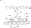
请参阅图1,本发明第一实施例提供一种场发射显示器10,其包括一阴极基板104,一栅极电极108,一第一绝缘层110,一阴极电极112,一阴极发射层116,一聚焦电极118,一阳极基板102,一阳极电极120,以及一荧光粉层122。其中,所述阴极基板104,栅极电极108,第一绝缘层110,阴极电极112,阴极发射层116,聚焦电极118构成该场发射显示器10的场发射阴极装置100。1, the first embodiment of the present invention provides a
所述阳极基板102与所述阴极基板104相对且间隔设置。所述阳极基板102与阴极基板104之间定义一真空空间106以收容所述栅极电极108,第一绝缘层110,阴极电极112,阴极发射层116,聚焦电极118,阳极电极120,和荧光粉层122。所述栅极电极108设置于阴极基板104相对于阳极基板102的一表面。所述第一绝缘层110设置于所述栅极电极108远离阴极基板104的一表面,且该第一绝缘层110定义一第一开孔1102,以使栅极电极108在对应所述第一开孔1102的位置暴露,并面对所述阳极基板102设置。所述阴极电极112设置于所述第一绝缘层110远离所述阴极基板104的一表面,并通过所述第一绝缘层110与所述栅极电极108间隔设置,且该阴极电极112定义一与所述第一开孔1102连通的第二开孔1122。所述阴极发射层116设置于阴极电极112远离所述阴极基板104的一表面,且与阴极电极112电连接。优选地,所述阴极发射层116仅设置于所述阴极电极112表面靠近第二开孔1122的位置。所述阴极发射层116定义一与第二开孔1122连通的第三开孔1162。所述阳极电极120设置于所述阳极基板102相对于阴极基板104的表面。所述荧光粉层122设置于阳极电极120表面。所述聚焦电极118设置于阴极电极112与阳极电极120之间,且定义一第四开孔1182,以使部分阴极电极112与阴极发射层116暴露。The
所述阴极基板104的材料可以为硅、玻璃、陶瓷、塑料或聚合物。所述阴极基板104的形状与厚度不限,可以根据实际需要选择。优选地,所述阴极基板104的形状为正方形或矩形。本实施例中,所述阴极基板104为一正方形玻璃板。The material of the
所述栅极电极108为一导电层,且其厚度和大小可以根据实际需要选择。所述栅极电极108可以仅设置于阴极基板104通过第一开孔1102暴露的表面,也可以延伸至第一绝缘层110与阴极基板104之间。所述栅极电极108与第一开孔1102对应的位置还可以具有一突起结构(图未示),以降低开启电压。所述栅极电极108的材料可以为单质金属、金属合金、氧化铟锡或导电浆料等。可以理解,当阴极基板104为硅片时,该栅极电极108可以为一硅掺杂层。本实施例中,所述栅极电极108为一厚度为20微米的铝膜。该铝膜通过磁控溅射法沉积于阴极基板104表面。The
所述第一绝缘层110设置于所述阴极电极112与栅极电极108之间,用于使所述阴极电极112与栅极电极108之间电性绝缘。所述第一绝缘层110的材料可以为树脂、厚膜曝光胶、玻璃、陶瓷、绝缘氧化物或上述材料的混合物等。所述绝缘氧化物包括二氧化硅、三氧化二铝或氧化铋等,所述第一绝缘层110的厚度和形状可以根据实际需要选择。所述第一绝缘层110可以直接设置于阴极基板104表面,也可设置于栅极电极108表面。所述第一绝缘层110为一具有通孔的层状结构,且该通孔定义为所述第一开孔1102。可以理解,如果第一绝缘层110没有开孔,而阴极电极112具有开孔时,所述阴极发射层116发射的向栅极电极108方向运动的少数电子会在第一绝缘层110表面积累,从而影响栅极电极108的电场分布。而所述第一开孔1102可以使阴极发射层116发射的向栅极电极108方向运动的少数电子达到栅极电极108,并通过栅极电极108导走。本实施例中,所述第一绝缘层110为一厚度为100微米的光刻胶设置于玻璃板表面,且其定义有一圆形通孔作为第一开孔1102。所述栅极电极108设置于所述第一绝缘层110与阴极基板104并将第一开孔1102覆盖。The first insulating
所述阴极电极112设置于第一绝缘层110远离阴极基板104的表面。所述阴极电极112为一导电层,其材料可以为单质金属、金属合金、氧化铟锡(ITO)或导电浆料等。所述阴极电极112的厚度和大小可以根据实际需要选择。具体地,所述阴极电极112可以为一具有通孔的层状结构,且该通孔定义所述第二开孔1122。所述第二开孔1122与第一开孔1102对应设置且相互连通。优选地,所述第二开孔1122与第一开孔1102同轴设置且具有相同的孔径。由于所述阴极电极112具有第二开孔1122,因此,所述栅极电极108产生的电场可以通过第一开孔1102和第二开孔1122渗透到阴极发射层116表面,并使阴极发射层116发射电子。本实施例中,所述阴极电极112为一铝导电层,且具有一圆形通孔作为第二开孔1122。The
请进一步参见图2,所述阴极发射层116仅设置在所述阴极电极112靠近第二开孔1122位置的表面,且所述阴极发射层116为一环形结构,其定义一第三开孔1162。所述阴极发射层116仅设置于阴极电极112面对阳极电极120且通过第四开孔1182暴露的表面。所述阴极发射层116可以设置于阴极电极112通过第四开孔1182暴露的部分表面或暴露的全部表面。优选地,所述阴极发射层116为一圆环形。所述第三开孔1162与上述第二开孔1122与第一开孔1102对应设置且相互连通,优选地,所述第三开孔1162与上述第二开孔1122以及第一开孔1102的孔径相同,即第三开孔1162的孔壁与上述第二开孔1122以及第一开孔1102的孔壁平齐。可以理解,由于阴极发射层116靠近第二开孔1122设置,所以栅极电极108产生的电场可以通过第二开孔1122渗透到阴极发射层116的整个表面,从而使得整个阴极发射层116发射电子。Please refer further to FIG. 2 , the
所述阴极发射层116包括多个电子发射体,如碳纳米管、纳米碳纤维、或硅纳米线等。进一步,所述阴极发射层116的表面可进一步设置一层抗离子轰击材料以提高其稳定性和寿命。所述抗离子轰击材料可选择为碳化锆、碳化铪及六硼化镧等中的一种或多种。本实施例中,所述阴极发射层116为一环形碳纳米管浆料层。所述碳纳米管浆料包括碳纳米管、低熔点玻璃粉以及有机载体。其中,有机载体在烘烤过程中蒸发,低熔点玻璃粉在烘烤过程中熔化并将碳纳米管固定于阴极电极112表面。The
所述聚焦电极118可以为金属栅网或导电层。所述聚焦电极118设置于阴极电极112与阳极电极120之间,且定义一第四开孔1182,以使阴极电极112靠近第二开孔1122的部分表面通过第四开孔1182暴露。所述聚焦电极118可以通过一第二绝缘层114与阴极电极112间隔设置并电性绝缘。所述第二绝缘层114的材料与所述第一绝缘层110相同,其厚度和形状可以根据实际需要选择。所述第二绝缘层114设置于阴极电极112远离所述阴极基板104的表面。所述第二绝缘层114定义一与第四开孔1182相通的第五开孔1142以使所述部分阴极电极112靠近第二开孔1122的部分表面暴露,从而使得所述阴极发射层116暴露并直接面对所述阳极基板102设置。本实施例中,所述第四开孔1182与第五开孔1142同轴设置且孔径相同。可以理解,当所述聚焦电极118为具有自支撑的金属栅网时,所述聚焦电极118也可以悬空设置于阴极电极112与阳极电极120之间。所述聚焦电极118的材料可以为金属、合金、氧化铟锡(ITO)或导电浆料等。所述聚焦电极118的厚度和大小可以根据实际需要选择。所述聚焦电极118用来汇聚所述阴极发射层116发射的电子。The focusing
所述阳极基板102为一透明基板,其形状与厚度不限,可以根据实际需要选择。优选地,所述阳极基板102的形状为正方形或矩形。所述阳极基板102和阴极基板104之间可以通过绝缘条(图未示)缝接以定义所述真空空间106。本实施例中,所述阳极基板102为一正方形玻璃板。The
所述阳极电极120为一透明导电层,如:碳纳米管膜,氧化铟锡薄膜或铝膜。所述阳极电极120的形状与厚度不限,可以根据实际需要选择。本实施例中,所述阳极电极120为一厚度100微米的氧化铟锡薄膜。The
所述荧光粉层122可以设置于阳极电极120远离阳极基板102的表面或设置于阳极电极120与阳极基板102之间。所述荧光粉层122的形状与厚度不限,可以根据实际需要选择。优选地,所述荧光粉层122的形状为圆形,且其半径大于等于所述阴极发射层116的内半径小于等于所述阴极发射层116的外半径。本实施例中,所述荧光粉层122为圆形,且其半径等于所述阴极发射层116的外半径。The
所述场发射显示器10工作时,所述阴极电极112接零电位(接地),所述栅极电极108施加一正电压V1,所述阳极电极120施加一正电压V2,所述聚焦电极118施加一负电压V3。所述栅极电极108的工作电压V1为10伏特~100伏特,所述阳极电极120的工作电压V2为500伏特~5000伏特,所述聚焦电极118的工作电压V3为负5伏特~负50伏特。所述栅极电极108产生的电场可以通过第二开孔1122渗透到阴极发射层116表面,并使阴极发射层116发射电子。所述电子在阳极电极120的电场力作用下射向阳极电极120并形成电子束124。由于所述聚焦电极118施加一负电压,该负电压对电子具有排斥作用,从而起到汇聚电子束124的作用。When the
进一步,所述场发射显示器10还可以包括一二次电子发射层126以提高场发射阴极装置100的电子发射效率。所述二次电子发射层126设置于第一开孔1102内的栅极电极108表面。所述二次电子发射层126的材料包括氧化镁(MgO)、氧化铍(BeO)、氟化镁(MgF2)、氟化铍(BeF2)、氧化铯(CsO)以及氧化钡(BaO)中的一种或几种,其厚度和大小可以根据实际需要选择。所述二次电子发射层126可以通过涂敷、电子束蒸发、热蒸发或磁控溅射等方法形成于栅极电极108的表面。可以理解,所述二次电子发射层126的表面还可以形成有凹凸结构以增加二次电子发射层126的面积,可提高二次电子发射效率。本实施例中,所述二次电子发射层126为一厚度为约5微米的氧化钡层。Further, the
请进一步参阅图3,本发明第一实施例进一步介绍包括多像素单元的场发射显示器10的实现方式。具体地,所述场发射显示器10包括一共用的阴极基板104,多个条形栅极电极108,一共用的第一绝缘层110,多个条形阴极电极112,多个圆环形阴极发射层116,一共用的聚焦电极118,一共用的阳极基板102,一共用的阳极电极120,以及多个圆形荧光粉层122。Please refer to FIG. 3 further, the first embodiment of the present invention further introduces the implementation of the
所述多个条形栅极电极108平行且等间隔设置于所述阴极基板104的表面。所述多个条形阴极电极112平行且等间隔设置,且该多个条形阴极电极112与多个条形栅极电极108异面垂直且交叉设置。所述栅极电极108与阴极电极112的交叉区域定义一像素区域。所述阴极电极112与像素区域相对应处定义一第二开孔1122。所述第一绝缘层110设置于所述多个栅极电极108与所述多个阴极电极112之间,且该第一绝缘层110与像素区域相对应处定义多个第一开孔1102。可以理解,所述第一绝缘层110也可以为多个间隔设置的绝缘条,优选地,绝缘条的形状与条形栅极电极108或条形阴极电极112的形状相同。所述第一开孔1102与第二开孔1122对应且相通设置,以使栅极电极108暴露。所述第二绝缘层114设置于所述多个条形阴极电极112表面,且与像素区域一一对应定义多个第五开孔1142,以使阴极发射层116部分暴露。可以理解,所述第二绝缘层114也可以为多个间隔设置的绝缘条,优选地,绝缘条的形状与条形阴极电极112的形状相同。所述多个圆环形阴极发射层116与像素区域一一对应设置,且每个圆环形阴极发射层116设置于阴极电极112通过第五开孔1142暴露的表面。所述圆环形阴极发射层116的第三开孔1162与第二开孔1122对应且相通设置。所述聚焦电极118设置于第二绝缘层114表面,且定义多个与第五开孔1142对应的第四开孔1182。所述聚焦电极118可以为一具有多个第四开孔1182整体导电层,或多个间隔设置且具有第四开孔1182的导电条。所述阳极电极120为一设置于阳极基板102表面的一整层透明导电层。所述多个圆形形荧光粉层122设置于阳极电极120表面,且与像素区域一一对应设置或与阴极发射层116一一对应设置。进一步,所述多个圆形形荧光粉层122之间还可以设置黑色矩阵以提高场发射显示器10的对比度。The plurality of strip-shaped
请参阅图4,为本发明第二实施例的场发射显示器10的显示效果。本发明实施例采用圆环形阴极发射层116,可以得到发光均匀的圆形像素点。Please refer to FIG. 4 , which shows the display effect of the
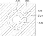
请参阅图5,本发明第二实施例提供一种场发射显示器20,其包括一阴极基板204,一栅极电极208,一第一绝缘层210,一阴极电极212,一阴极发射层216,一第二绝缘层214,一聚焦电极218,一阳极基板202,一阳极电极220,以及一荧光粉层222。其中,所述阴极基板204,栅极电极208,第一绝缘层210,阴极电极212,阴极发射层216,聚焦电极218构成该场发射显示器20的场发射阴极装置200。本发明第二实施例提供的场发射显示器20与本发明第一实施例提供一种场发射显示器10的结构基本相同,其区别在于所述阴极电极212进一步定义一个或多个环绕第二开孔2122的第六开孔2124。5, the second embodiment of the present invention provides a
请进一步参阅图6至8,所述第六开孔2124将第二开孔2122基本环绕。所述第六开孔2124将所述阴极电极212分成间隔设置的一第一部分2128和一第二部分2126。所述第一部分2128设置于第二绝缘层214与第一绝缘层210之间。所述第二部分2126设置于阴极发射层216与第一绝缘层210之间。所述阴极发射层216仅设置于第二部分2126表面。所述第二开孔2122由第二部分2126定义。所述第一部分2128和第二部分2126之间通过至少一连接部2127连接,以实现电导通。所述第六开孔2124的形状不限,可以根据第二开孔2122的形状选择。当第二开孔2122为圆形时,所述第六开孔2124可以为一如图6所示的环形开孔、两个如图7所示的半环形开孔、或多个如图8所示的弧形开孔。可以理解,当第二开孔2122为方形时,所述第六开孔2124可以为与方形第二开孔2122的四边平行的长条形开孔。本实施例中,所述第二开孔2122为圆形,所述第六开孔2124为四个围绕第二开孔2122的弧形开孔,且相邻两个第六开孔2124之间的部分为连接部2127。所述第六开孔2124的内径大于等于所述阴极发射层216的外径,所述第六开孔2124的外径小于等于所述第四开孔2182的孔径。优选地,所述第六开孔2124的内径等于所述阴极发射层216的外径,所述第六开孔2124的外径等于所述第四开孔2182的孔径。可以理解,所述第六开孔2124可以使得栅极电极208的电场从第六开孔2124渗透到所述阴极发射层216的表面,从而提高了阴极发射层216的电子发射效率。Please refer to FIGS. 6 to 8 further, the
进一步,所述第一绝缘层210还可以定义一个或多个与第六开孔2124对应的第七开孔2104。所述第七开孔2104将第一开孔2102基本环绕。所述栅极电极208对应该第七开孔2104与第六开孔2124的位置的部分表面暴露,从而使得使阴极发射层216发射的向栅极电极208方向运动的少数电子达到栅极电极208,并通过栅极电极208导走。Further, the first insulating
所述场发射显示器10具有以下优点:第一,所述第一绝缘层设置有一第一开孔,所述阴极电极设置有一第二开孔,所述第一开孔与第二开孔对应设置且相互连通,使所述栅极电极对应该开孔位置的表面暴露,所述阴极发射层仅设置在所述阴极电极靠近所述第二开孔位置的表面,所以栅极电极的电场可以通过阴极电极的第二开孔渗透到阴极发射层表面,以使环形阴极发射层发射电子,从而得到发光均匀的圆形像素点。而且阴极发射层发射的向栅极电极电极方向运动的电子可以达到栅极电极,并通过栅极电极导走,从而避免在第一绝缘层表面积累电荷,影响栅极电极的电场分布。第二,通过在第一开孔内的栅极电极表面设置二次电子发射层,可以提高场发射阴极装置的电子发射效率。第三,所述阴极电极定义一个或多个环绕第二开孔的第六开孔,使得栅极电极的电场从第六开孔渗透到所述阴极发射层的表面,从而提高了阴极发射层的电子发射效率。The
另外,本领域技术人员还可在本发明精神内作其它变化,当然这些依据本发明精神所作的变化,都应包含在本发明所要求保护的范围内。In addition, those skilled in the art can also make other changes within the spirit of the present invention. Of course, these changes made according to the spirit of the present invention should be included in the scope of protection claimed by the present invention.
Claims (10)
Translated fromChinesePriority Applications (3)
| Application Number | Priority Date | Filing Date | Title |
|---|---|---|---|
| CN201010589777ACN102074440B (en) | 2010-12-15 | 2010-12-15 | Field-emission cathode device and field-emission display |
| JP2011034423AJP5538266B2 (en) | 2010-12-15 | 2011-02-21 | Field emission cathode device and field emission display device using the same |
| US13/081,340US8710729B2 (en) | 2010-12-15 | 2011-04-06 | Field emission cathode device and field emission display using the same |
Applications Claiming Priority (1)
| Application Number | Priority Date | Filing Date | Title |
|---|---|---|---|
| CN201010589777ACN102074440B (en) | 2010-12-15 | 2010-12-15 | Field-emission cathode device and field-emission display |
Publications (2)
| Publication Number | Publication Date |
|---|---|
| CN102074440A CN102074440A (en) | 2011-05-25 |
| CN102074440Btrue CN102074440B (en) | 2012-08-29 |
Family
ID=44032939
Family Applications (1)
| Application Number | Title | Priority Date | Filing Date |
|---|---|---|---|
| CN201010589777AActiveCN102074440B (en) | 2010-12-15 | 2010-12-15 | Field-emission cathode device and field-emission display |
Country Status (3)
| Country | Link |
|---|---|
| US (1) | US8710729B2 (en) |
| JP (1) | JP5538266B2 (en) |
| CN (1) | CN102074440B (en) |
Families Citing this family (6)
| Publication number | Priority date | Publication date | Assignee | Title |
|---|---|---|---|---|
| JP2906099B2 (en) | 1992-12-21 | 1999-06-14 | 横浜ゴム株式会社 | Manufacturing method of pneumatic radial tire |
| CN104103470A (en)* | 2014-07-31 | 2014-10-15 | 电子科技大学 | Polycrystal hexaboride annular field emission cathode and preparation method thereof |
| US10175005B2 (en)* | 2015-03-30 | 2019-01-08 | Infinera Corporation | Low-cost nano-heat pipe |
| US10176960B2 (en)* | 2017-04-07 | 2019-01-08 | Elwha Llc | Devices and methods for enhancing the collection of electrons |
| CN110854007A (en)* | 2019-11-12 | 2020-02-28 | 中山大学 | Flat-panel X-ray source based on X-ray micro-pixel unit and preparation method thereof |
| TW202232541A (en)* | 2020-09-30 | 2022-08-16 | 美商Ncx公司 | Field emission cathode device and method for forming a field emission cathode device |
Family Cites Families (9)
| Publication number | Priority date | Publication date | Assignee | Title |
|---|---|---|---|---|
| JP2001043789A (en)* | 1999-07-30 | 2001-02-16 | Sony Corp | Cold cathode electric field electron emitting element, manufacture thereof, and cold cathode electric field electron emitting display device |
| JP2002100279A (en)* | 2000-09-22 | 2002-04-05 | Canon Inc | Electron emitting device, electron source, image forming apparatus, and method of driving electron emitting device |
| JP5011619B2 (en) | 2001-08-01 | 2012-08-29 | 日本電気株式会社 | Electron emission film and field electron emission device |
| JP3727894B2 (en)* | 2002-03-08 | 2005-12-21 | 日本放送協会 | Field emission electron source |
| KR20050066758A (en)* | 2003-12-27 | 2005-06-30 | 삼성에스디아이 주식회사 | Field emission display device with grid plate |
| KR20050096536A (en)* | 2004-03-31 | 2005-10-06 | 삼성에스디아이 주식회사 | Electron emission display with grid electrode |
| KR20050111706A (en) | 2004-05-22 | 2005-11-28 | 삼성에스디아이 주식회사 | Field emission display and method for manufacturing the same |
| JP4741449B2 (en)* | 2006-10-30 | 2011-08-03 | 日本放送協会 | Cold cathode, cold cathode array and field emission display |
| CN100561652C (en)* | 2007-06-19 | 2009-11-18 | 中原工学院 | Flat panel display with gate-controlled cathode structure in ring and its manufacturing process |
- 2010
- 2010-12-15CNCN201010589777Apatent/CN102074440B/enactiveActive
- 2011
- 2011-02-21JPJP2011034423Apatent/JP5538266B2/enactiveActive
- 2011-04-06USUS13/081,340patent/US8710729B2/enactiveActive
Also Published As
| Publication number | Publication date |
|---|---|
| US20120153802A1 (en) | 2012-06-21 |
| JP5538266B2 (en) | 2014-07-02 |
| CN102074440A (en) | 2011-05-25 |
| JP2012129180A (en) | 2012-07-05 |
| US8710729B2 (en) | 2014-04-29 |
Similar Documents
| Publication | Publication Date | Title |
|---|---|---|
| CN102074440B (en) | Field-emission cathode device and field-emission display | |
| JP5595854B2 (en) | Field emission cathode device and field emission display device | |
| TWI471890B (en) | Field emission cathode device and driving method of the field emission cathode device | |
| US7714493B2 (en) | Field emission device and field emission display employing the same | |
| CN101635239B (en) | Field emission cathode device and field emission display | |
| TWI416571B (en) | Field emission cathode device and field emission display | |
| CN100521056C (en) | Electron emission device | |
| US20070120459A1 (en) | Field emission display device | |
| KR100284539B1 (en) | KAIST Field Emitter Display | |
| CN101170041A (en) | field emission display | |
| CN100576411C (en) | Separator for electron emission display and manufacturing method thereof | |
| CN102074441A (en) | Field-emission cathode device and field-emission display | |
| KR20070075659A (en) | Method for manufacturing an electron emitting device, an electron emitting device manufactured thereby, a backlight device and an electron emitting display device using the same | |
| TWI407477B (en) | Field emission device | |
| TWI390575B (en) | Field emission cathode structure and display device for using the same | |
| TWI407478B (en) | Method for making field emission device | |
| KR19990032988A (en) | Field emission device and image display device using same | |
| TWI415157B (en) | Field emission cathode device and field emission display | |
| KR101072998B1 (en) | Electron emission display device | |
| TWI421894B (en) | Metal mesh, field emission device and field emission display | |
| KR100532999B1 (en) | Carbon nanotube field emission device having a field shielding plate | |
| CN101908457A (en) | Metal grid and field emission device and field emission display | |
| KR20070078916A (en) | Electron-emitting device | |
| TW201007805A (en) | Field emission cathode device and field emission display | |
| KR20070014622A (en) | Electron-emitting device |
Legal Events
| Date | Code | Title | Description |
|---|---|---|---|
| C06 | Publication | ||
| PB01 | Publication | ||
| C10 | Entry into substantive examination | ||
| SE01 | Entry into force of request for substantive examination | ||
| C14 | Grant of patent or utility model | ||
| GR01 | Patent grant |