CN102073596A - Method for managing reconfigurable on-chip unified memory aiming at instructions - Google Patents
Method for managing reconfigurable on-chip unified memory aiming at instructionsDownload PDFInfo
- Publication number
- CN102073596A CN102073596ACN2011100073102ACN201110007310ACN102073596ACN 102073596 ACN102073596 ACN 102073596ACN 2011100073102 ACN2011100073102 ACN 2011100073102ACN 201110007310 ACN201110007310 ACN 201110007310ACN 102073596 ACN102073596 ACN 102073596A
- Authority
- CN
- China
- Prior art keywords
- memory
- reconfigurable
- cache
- spm
- program
- Prior art date
- Legal status (The legal status is an assumption and is not a legal conclusion. Google has not performed a legal analysis and makes no representation as to the accuracy of the status listed.)
- Granted
Links
Images


Classifications
- Y—GENERAL TAGGING OF NEW TECHNOLOGICAL DEVELOPMENTS; GENERAL TAGGING OF CROSS-SECTIONAL TECHNOLOGIES SPANNING OVER SEVERAL SECTIONS OF THE IPC; TECHNICAL SUBJECTS COVERED BY FORMER USPC CROSS-REFERENCE ART COLLECTIONS [XRACs] AND DIGESTS
- Y02—TECHNOLOGIES OR APPLICATIONS FOR MITIGATION OR ADAPTATION AGAINST CLIMATE CHANGE
- Y02D—CLIMATE CHANGE MITIGATION TECHNOLOGIES IN INFORMATION AND COMMUNICATION TECHNOLOGIES [ICT], I.E. INFORMATION AND COMMUNICATION TECHNOLOGIES AIMING AT THE REDUCTION OF THEIR OWN ENERGY USE
- Y02D10/00—Energy efficient computing, e.g. low power processors, power management or thermal management
Landscapes
- Memory System Of A Hierarchy Structure (AREA)
Abstract
Translated fromChineseDescription
Translated fromChinese技术领域technical field
本发明涉及一种可重构片上统一存储器,尤其涉及一种利用虚存机制实现对该可重构片上统一存储器的动态管理,具体给出该存储器的电路和动态管理方法。The invention relates to a reconfigurable on-chip unified memory, in particular to a dynamic management of the reconfigurable on-chip unified memory by using a virtual memory mechanism, and specifically provides a circuit and a dynamic management method of the memory.
背景技术Background technique
随着微电子技术的发展,以SoC(System-on-a-Chip)为基础的嵌入式计算平台日益成熟。然而,由于处理器速度与外部存储器速度的差距不断增大,SoC存储子系统已经成为系统性能、功耗和成本的瓶颈。因此如何优化存储子系统的架构及管理策略,一直是嵌入式研究的热点。With the development of microelectronics technology, the embedded computing platform based on SoC (System-on-a-Chip) is becoming more and more mature. However, due to the increasing gap between processor speed and external memory speed, the SoC memory subsystem has become the bottleneck of system performance, power consumption and cost. Therefore, how to optimize the architecture and management strategy of the storage subsystem has always been a hot spot in embedded research.
Cache与SPM(Scratch-Pad Memory,便签存储器)是最常见的传统的片上存储器。Cache由硬件管理,大部分情况下对软件透明,能自动装载最近访问的指令和数据到片上存储器中。然而,Cache的高功耗、占用面积大、程序执行时间不可预知等不足一直限制其在嵌入式系统中的广泛运用。尤其是Cache的组关联特性,可能导致被映射到同一Cache行的不同程序内容,由于访存规律,反复相互替换,从而增大了系统性能与能耗的开销,即出现Cache抖动。与Cache相比,SPM是一种高速片上存储器,通常由SRAM实现,是现代嵌入式系统中一个非常重要的系统框架设计考虑因素。SPM处于处理器可直接访问的地址空间之内,由于传统的SPM控制器不包含任何辅助管理数据的逻辑电路,SPM中的所有内容必须经由软件显式的管理,相对于对程序员透明的Cache,增加了程序管理的复杂性。由于没有管理逻辑电路带来的额外代价,相较于传统Cache,SPM硬件实现更为简单、单次访问功耗更低、占用芯片面积更小而且访问时间可预知。综上,Cache和SPM各具优势且存在互补性,因此对讲Cache和SPM进行统一配置管理的可重构片上统一存储器进行研究,可以充分利用两者优势,从而最大限度降低系统能耗、提升系统性能。Cache and SPM (Scratch-Pad Memory) are the most common traditional on-chip memories. Cache is managed by hardware, transparent to software in most cases, and can automatically load recently accessed instructions and data into on-chip memory. However, the shortcomings of Cache, such as high power consumption, large occupied area, and unpredictable program execution time, have always limited its wide application in embedded systems. In particular, the group-association feature of Cache may cause different program contents mapped to the same Cache row to be replaced repeatedly due to memory access rules, thus increasing system performance and energy consumption overhead, that is, Cache jitter. Compared with Cache, SPM is a high-speed on-chip memory, usually implemented by SRAM, which is a very important system framework design consideration in modern embedded systems. The SPM is located in the address space directly accessible by the processor. Since the traditional SPM controller does not contain any logic circuits for auxiliary data management, all content in the SPM must be explicitly managed by software, compared to the Cache which is transparent to the programmer. , increasing the complexity of program management. Since there is no additional cost brought by the management logic circuit, compared with the traditional Cache, the SPM hardware implementation is simpler, the power consumption of a single access is lower, the chip area is smaller, and the access time is predictable. To sum up, Cache and SPM have their own advantages and are complementary. Therefore, research on reconfigurable on-chip unified memory that performs unified configuration management on Cache and SPM can make full use of the advantages of both, thereby minimizing system energy consumption and improving system performance.
一些针对嵌入式片上存储器的研究的主要分析单纯配置Cache或单纯配置SPM的架构,不能很好的利用两者互补的特性。直接将仅针对SPM的优化算法或仅针对Cache的优化算法运用到可重构片上统一存储器中,不能达到整体功耗和性能最优化,在一种存储体上取得的优化收益可能被另一种存储器的开销所抵消,甚至引入更多系统性能与能耗的额外开销。例如针对SPM的优化算法将某段主存的内容搬运到SPM,从而得到了性能与能耗的收益。然而搬运代码本身可能对指令Cache造成污染、引起Cache优化算法的失效,从而造成额外的Cache缺失,抵消SPM的优化收益。Some researches on embedded on-chip memory mainly analyze the structure of only configuring Cache or SPM, which cannot make good use of the complementary characteristics of the two. Directly applying the optimization algorithm only for SPM or only for Cache to the reconfigurable on-chip unified memory cannot achieve the optimization of overall power consumption and performance, and the optimization benefits obtained on one memory bank may be replaced by another The overhead of the memory is offset, and even introduces more overhead of system performance and energy consumption. For example, the optimization algorithm for SPM moves the content of a certain section of main memory to SPM, thereby obtaining performance and energy consumption benefits. However, moving the code itself may pollute the instruction cache and cause the cache optimization algorithm to fail, thereby causing additional cache misses and offsetting the optimization benefits of SPM.
Cache缺失时需要实际访外存操作并将新的内容换入Cache行,开销较大,这被称为Cache缺失的惩罚。由于Cache的组关联特性,被映射到同一Cache行内容可能反复相互替换,带来大量的访存操作,从而导致系统性能急剧降低,系统能耗急剧增加,这就是Cache的冲突。通过增大Cache容量、增大组关联数等方法,可以减小Cache冲突,但是这样又会引入新的芯片面积并提升单次Cache读写时间及能耗,而且高关联度的Cache中某些路中存在大量的空闲的存储块,浪费了宝贵的片上存储资源。目前有研究指出Cache冲突是造成系统性能和能耗瓶颈的重要原因,因此他们将容易引起Cache冲突的程序段放入SPM,以此得到性能和能耗的收益。将容易引起Cache冲突的页选入SPM中,不仅可以通过降低Cache冲突而降低系统能耗,提升系统性能,还能由单次访问SPM与Cache的能耗差获得更多收益。但是这些研究都是基于静态的电路设计,即在程序执行中Cache的关联度和SPM的大小不会改变。研究表明,不同的应用程序甚至统一程序的不同阶段具有不同的访存特性,这种固定的存储架构并不能适应访存特性的变化。When the cache is missing, it needs to actually access the external memory and replace the new content into the cache line, which is expensive, which is called the penalty of cache missing. Due to the group association feature of Cache, the content mapped to the same Cache line may be replaced repeatedly, resulting in a large number of memory access operations, resulting in a sharp decrease in system performance and a sharp increase in system energy consumption. This is the conflict of Cache. Cache conflicts can be reduced by increasing the Cache capacity, increasing the number of group associations, etc., but this will introduce a new chip area and increase the time and energy consumption of a single Cache read and write, and some of the high-association Cache There are a large number of idle storage blocks in the road, wasting precious on-chip storage resources. At present, studies have pointed out that cache conflicts are an important cause of system performance and energy consumption bottlenecks, so they put the program segments that are likely to cause cache conflicts into SPM to obtain performance and energy consumption benefits. Selecting pages that are prone to cache conflicts into SPM can not only reduce system energy consumption and improve system performance by reducing cache conflicts, but also gain more benefits from the energy consumption difference between SPM and Cache for a single access. But these studies are based on static circuit design, that is, the associativity of Cache and the size of SPM will not change during program execution. Studies have shown that different applications and even different stages of a unified program have different memory access characteristics, and this fixed storage architecture cannot adapt to changes in memory access characteristics.
由于对SPM内容的更改需要软件显示的进行,因此一般对SPM进行动态管理的研究都是通过“打桩”的形式,即在需要优化的程序核心循环前后,手工插入代码搬运指令,从而完成对程序内容的换入换出。在程序映像中插入新的指令,需要依赖对源码的分析,并且新的指令很可能引起共存架构中Cache行为的变化,例如产生更多的冲突。Since the change of the SPM content needs to be displayed by the software, the research on the dynamic management of the SPM is usually carried out in the form of "piling", that is, manually inserting code handling instructions before and after the core cycle of the program that needs to be optimized, so as to complete the program. Swapping in and out of content. Inserting new instructions into the program image needs to rely on the analysis of the source code, and the new instructions are likely to cause changes in the behavior of the Cache in the coexistence architecture, such as generating more conflicts.
目前针对Cache和SPM共存架构中指令部分的研究,一般需要对程序进行侵入式的分析,需要在用户程序中插入、修改部分代码,以实现在程序执行过程中内容的动态换入换出。针对可重构架构的研究多是针对可重构Cache的研究,在程序运行过程中尝试性的改变Cache的参数以求得能耗最低,但无法对程序性能进行提高。到目前为止,还未有相关研究涉及针对程序指令部分,利用虚存管理方式,动态管理可重构片上统一存储器的方法。At present, the research on the instruction part of the coexistence architecture of Cache and SPM generally requires intrusive analysis of the program, and it is necessary to insert and modify some codes in the user program to realize the dynamic swapping in and out of the content during program execution. Most of the research on reconfigurable architecture is on reconfigurable Cache. During the running of the program, the parameters of Cache are tried to be changed to obtain the lowest energy consumption, but the performance of the program cannot be improved. So far, there is no relevant research involving the method of dynamically managing the reconfigurable on-chip unified memory by using the virtual memory management method for the program instruction part.
发明内容Contents of the invention
技术问题: 本发明的目的在于克服现有片上存储子系统的不足,采用一种可重构的片上统一存储器,提出一种利用虚存机制实现对可重构存储器动态管理的方法,根据程序执行的阶段性动态配置可重构存储器中Cache部分和SPM部分的参数,将引起Cache冲突的指令页和频繁访问的指令页映射到SPM部分中,从而降低由冲突带来的额外访存和Cache比较逻辑的额外能耗,最终降低系统能耗并提高微处理器运行的速度。Technical problem: The purpose of the present invention is to overcome the deficiencies of the existing on-chip storage subsystem, adopt a reconfigurable on-chip unified memory, and propose a method for realizing dynamic management of the reconfigurable memory by using a virtual memory mechanism. The phased dynamic configuration can reconfigure the parameters of the Cache part and the SPM part of the memory, and map the instruction pages that cause Cache conflicts and frequently accessed instruction pages to the SPM part, thereby reducing the extra memory access and Cache comparison caused by conflicts Additional power consumption of the logic, which ultimately reduces system power consumption and increases the speed at which the microprocessor operates.
技术方案:本发明的利用虚存机制动态管理可重构片上统一存储器的方法通过在应用程序执行过程中对处理器读取指令的跟踪及对可重构存储器中的高速缓冲存储器Cache部分行为的跟踪,得到指令执行特性以及Cache中指令命中和缺失的时间和空间分布,进而对指令Cache在不同阶段的相变行为图并对其进行数学抽像,根据能耗目标函数、性能目标函数分别利用整数非线性规划的方法选出系统总能耗最优时的可重构存储器参数配置及每个指令页的分布状态;在程序执行中通过程序相变检测器产生相变中断,在每个阶段可重构片上统一存储器中Cache部分和便签存储器SPM(Scratch-Pad Memory)部分的结构,并通过对页表项入口的修改、直接内存访问可重构片上统一存储器控制器的配置,将合适的指令页映射到SPM存储器中,消除指令Cache冲突带来的额外访存以及频繁访问Cache带来的比较逻辑额外能耗。Technical solution: The method for dynamically managing the reconfigurable on-chip unified memory using the virtual memory mechanism of the present invention tracks the instruction read by the processor and monitors the behavior of the Cache part in the reconfigurable memory during the execution of the application program. Tracking to obtain the instruction execution characteristics and the time and space distribution of instruction hits and misses in the Cache, and then mathematically abstract the phase transition behavior diagram of the instruction Cache at different stages, according to the energy consumption objective function and performance objective function The integer nonlinear programming method selects the reconfigurable memory parameter configuration and the distribution status of each instruction page when the total energy consumption of the system is optimal; during program execution, a phase change interrupt is generated by the program phase change detector, and at each stage The structure of the Cache part and the SPM (Scratch-Pad Memory) part of the on-chip unified memory can be reconfigured, and the configuration of the on-chip unified memory controller can be reconfigured by modifying the page table entry and direct memory access. The instruction page is mapped to the SPM memory, eliminating the extra memory access caused by instruction cache conflicts and the extra energy consumption of comparison logic caused by frequent access to the cache.
利用程序执行不同阶段体现出不同的指令执行特性,将程序执行过程划分为不同的阶段;在不同的阶段中获取可重构存储器中Cache的相变行为图后,利用当前阶段指令的局部性,将Cache部分中利用率不高的路重构为SPM存储结构,将一段时间内最频繁引起指令Cache冲突以及频繁访问的指令地址空间重映射到SPM存储部分中,而在其收益不大时映射回主存。Using different stages of program execution to reflect different instruction execution characteristics, the program execution process is divided into different stages; after obtaining the phase change behavior diagram of the Cache in the reconfigurable memory in different stages, using the locality of instructions in the current stage, Restructure the low-utilization ways in the Cache part into SPM storage structures, and remap the instruction address spaces that most frequently cause instruction cache conflicts and frequent accesses to the SPM storage part for a period of time, and map them when the benefits are not large. back to main memory.
所说可重构片上统一存储器可以在程序运行过程中,通过配置可重构片上统一存储器控制器的当前配置信息寄存器,将可重构存储器中的Cache部分关闭某一路的Tag bank,并将其Data bank重构为SPM使用;或者将SPM中的某一bank对应的Tag bank打开重构为Cache使用,通过这种方式可以动态调整存储架构中Cache的关联度和SPM容量,同时在存储器控制器中还设置有专用于记录每个程序阶段的重构配置信息的配置信息寄存器组和记录SPM区域映射关系的SPM区域寄存器组,其作用是:The reconfigurable on-chip unified memory can close the tag bank of a certain way in the Cache part of the reconfigurable memory by configuring the current configuration information register of the reconfigurable on-chip unified memory controller during the running of the program, and turn it Data bank is reconstructed to be used by SPM; or the Tag bank corresponding to a certain bank in SPM is opened and reconstructed to be used by Cache. In this way, the association degree of Cache in the storage architecture and the capacity of SPM can be dynamically adjusted. There is also a configuration information register set dedicated to recording the reconstruction configuration information of each program stage and an SPM area register set recording the mapping relationship of the SPM area. Its functions are:
1)配置信息寄存器组负责记录可重构存储器在每个程序阶段所对应的Cache部分和SPM部分的配置信息,当程序相变检测器检测到程序阶段发生变化时,中断处理程序将该阶段所需的配置信息从该组寄存器装载到当前配置信息寄存器中,完成对可重构存储器的动态配置;1) The configuration information register group is responsible for recording the configuration information of the Cache part and the SPM part corresponding to each program stage of the reconfigurable memory. The required configuration information is loaded from this group of registers into the current configuration information register to complete the dynamic configuration of the reconfigurable memory;
2)SPM区域寄存器组负责记录每个程序阶段需要换入到SPM存储部分的指令页的物理地址,用于配置直接内存访问控制器将指令页从主存搬入到SPM存储部分,该组寄存器还将负责在某虚存页被换出SPM存储部分时用于恢复换入前的页表项;2) The SPM area register group is responsible for recording the physical address of the instruction page that needs to be swapped into the SPM storage part in each program stage, and is used to configure the direct memory access controller to move the instruction page from the main memory to the SPM storage part. This group of registers also It will be responsible for restoring the page table entry before swapping in when a virtual memory page is swapped out of the SPM storage part;
所说程序相变检测器在程序执行过程中统计指令的执行特性,并按照配置寄存器中配置的检测方式及阈值,在程序阶段性发生变化时产生相变中断,在中断处理程序中可以对可重构片上统一存储器进行配置,进而迎合程序不同阶段对存储架构的要求。The program phase change detector counts the execution characteristics of instructions during program execution, and generates a phase change interrupt when the program changes step by step according to the detection mode and threshold configured in the configuration register. Reconfigure the on-chip unified memory to meet the requirements of the storage architecture at different stages of the program.
可重构片上统一存储器包含Cache部分和SPM部分,这两部分可以在程序运行过程中动态的调整参数:Cache部分的关联度,SPM部分的容量。The reconfigurable on-chip unified memory includes a Cache part and an SPM part. These two parts can dynamically adjust parameters during program running: the associativity of the Cache part and the capacity of the SPM part.
所述的相变检测器通过实时检测处理器在运行程序过程中执行指令的特性,利用该特性的变化判断程序相变,记录相变序号并向处理器产生中断信号。The phase change detector detects in real time the characteristics of the instructions executed by the processor in the process of running the program, uses the change of the characteristics to judge the phase change of the program, records the sequence number of the phase change and generates an interrupt signal to the processor.
得到指令执行特性以及Cache中指令命中和缺失的时间和空间分布,利用程序执行时表现出来的阶段性,将一段时间内最频繁引起Cache冲突和最频繁访问的地址空间重映射到SPM存储器中,而在其收益不大时映射回主存。Obtain the instruction execution characteristics and the time and space distribution of instruction hits and misses in the Cache, and use the staged performance of the program execution to remap the address space that most frequently causes Cache conflicts and the most frequently accessed within a period of time to the SPM memory, And map back to main memory when its benefit is not large.
可重构统一片上存储器控制器在程序执行过程中利用其内部的直接内存访问控制器动态高效的将程序指令部分换入到SPM存储部分,利用片上AHB高速总线的Burst特性,避免通过处理器进行搬运对Cache的二次污染。The reconfigurable unified on-chip memory controller uses its internal direct memory access controller to dynamically and efficiently swap the program instruction part into the SPM storage part during program execution, and uses the Burst feature of the on-chip AHB high-speed bus to avoid processing by the processor. Handling secondary pollution to the Cache.
在可重构片上统一存储器控制器中设置了一组专用于记录每个程序阶段可重构存储器配置信息以及SPM存储部分地址映射关系的区域寄存器组:In the reconfigurable on-chip unified memory controller, a group of regional registers dedicated to recording the configuration information of the reconfigurable memory at each program stage and the address mapping relationship of the SPM storage part is set:
1)该组寄存器将负责在程序相变检测电路检测到程序阶段发生变化时,由中断处理程序将该阶段所需的配置信息装载到当前配置信息寄存器中,完成对可重构存储器的动态配置;1) This group of registers will be responsible for loading the configuration information required for this stage into the current configuration information register by the interrupt handler when the program phase change detection circuit detects a change in the program stage to complete the dynamic configuration of the reconfigurable memory ;
2)该组寄存器负责记录每个程序阶段需要换入到SPM存储部分的指令页的物理地址,用于配置直接内存访问控制器将指令页从主存搬入到SPM存储部分;2) This group of registers is responsible for recording the physical address of the instruction page that needs to be swapped into the SPM storage part in each program stage, and is used to configure the direct memory access controller to move the instruction page from the main memory to the SPM storage part;
3)该组寄存器将负责在某虚存页重映射在SPM存储部分时,记录其对应的主存地址,此地址将在该虚存页被换出SPM存储部分时用于恢复换入前的页表项。3) This group of registers will be responsible for recording the corresponding main memory address when a virtual memory page is remapped in the SPM storage part, and this address will be used to restore the value before swapping in when the virtual memory page is swapped out of the SPM storage part page table entry.
有益效果:本发明充分利用程序执行过程中的阶段性特点,创新性的提出了相变行为图的概念,通过对相变行为图的分析,动态的配置可重构片上统一存储器中的Cache部分和SPM部分的参数,适应程序执行每个阶段的访存特性,最大程度的降低系统能耗,并一定程度的提升系统性能。利用虚存管理的思想可以方便解决传统SPM优化技术中侵入性的修改程序代码布局的缺点。传统的优化技术多采用在程序中插入搬运指令将待优化的段动态搬运到SPM的办法,采用虚存管理的思想,就可以将实际的物理地址与程序在编译时分配使用的虚拟地址隔离开。这样,对于程序而言虚拟地址空间在优化前后都是连续的,但对于真实的硬件而言,已经将频繁访问的和引起Cache冲突的指令段部分重映射到SPM部分中,从而降低了Cache的访问次数和冲突次数,最终获得了性能和能耗上的收益。同时,利用虚存机制对程序进行管理,可以实现对程序非侵入式的分析和优化,即不需要在用户程序中显示的增加SPM的搬运代码,而在相变中断处理中通过配置DMA和修改页表来完成对程序内容的换入换出。本发明将虚存管理的机制和可重构片上统一存储器有机结合,获得相较于其他单一Cache优化或单一SPM优化更为可观的性能和能耗收益。Beneficial effects: the present invention makes full use of the staged characteristics in the program execution process, and innovatively proposes the concept of a phase change behavior diagram, through the analysis of the phase transition behavior diagram, dynamically configures the Cache part of the reconfigurable on-chip unified memory And the parameters of the SPM part adapt to the memory access characteristics of each stage of program execution, minimize system energy consumption, and improve system performance to a certain extent. Using the idea of virtual memory management can easily solve the shortcomings of intrusive modification of program code layout in traditional SPM optimization technology. The traditional optimization technology mostly adopts the method of inserting moving instructions in the program to dynamically move the segment to be optimized to SPM. Using the idea of virtual memory management, the actual physical address can be separated from the virtual address allocated and used by the program when compiling. . In this way, for the program, the virtual address space is continuous before and after optimization, but for the real hardware, the instruction segment that is frequently accessed and causes Cache conflicts has been remapped to the SPM part, thereby reducing the cache memory. The number of visits and the number of conflicts ultimately yield benefits in performance and energy consumption. At the same time, using the virtual memory mechanism to manage the program can realize non-intrusive analysis and optimization of the program, that is, there is no need to increase the handling code of SPM displayed in the user program, but in the phase change interrupt processing by configuring DMA and modifying The page table is used to complete the swapping in and out of the program content. The invention organically combines the virtual memory management mechanism with the reconfigurable on-chip unified memory, and obtains more considerable performance and energy consumption benefits than other single Cache optimization or single SPM optimization.
附图说明Description of drawings
图1为利用虚存机制实现对可重构片上统一存储器动态管理的系统框图;Figure 1 is a system block diagram for realizing the dynamic management of the reconfigurable on-chip unified memory by using the virtual memory mechanism;
图2为修改后的TLB页表项示意图;FIG. 2 is a schematic diagram of a modified TLB page table entry;
图3可重构片上统一存储器示意图;Figure 3 is a schematic diagram of a reconfigurable on-chip unified memory;
图4为相变行为图示意图;Fig. 4 is a schematic diagram of a phase transition behavior diagram;
图5为利用虚存机制对可重构片上统一存储器进行动态管理的方法的系统流程图。FIG. 5 is a system flowchart of a method for dynamically managing the reconfigurable on-chip unified memory by using a virtual memory mechanism.
具体实施方式Detailed ways
本发明方法具体可按以下步骤实现:The inventive method can specifically be realized according to the following steps:
(1)建立虚存管理的机制(1) Establish a virtual memory management mechanism
虚存管理机制可以通过修改页表项,形成物理分离、逻辑连续的地址空间,这样就可以实现将部分程序页的地址映射到可重构存储器的SPM部分中。相对于传统的动态SPM优化技术,利用虚存完成地址空间映射关系的更改,可以实现对程序源代码和编译后生成的二进制映像的完全非侵入式优化。为了适应对Cache和SPM动态管理的方法,提高SPM部分的利用率,本发明需要对原有的MMU硬件进行改进。通过修改TLB的译码逻辑,增加对512 Bytes/虚拟页、256 Bytes/虚拟页支持。传统的TLB仅支持最小1K Bytes/虚拟页的管理,而Cache是按行组织的,每行仅32-64Bytes,在程序执行的一段时间内出现指令Cache冲突或频繁访问的的地址空间大多小于传统TLB支持的最小虚存页大小,为了对优化粒度进行细化,提高SPM利用率,本发明将利用传统页表项入口中的保留位,修改TLB的Tag存储器和比较电路,实现对256 Bytes/虚拟页和512 Bytes/虚拟页的支持。The virtual memory management mechanism can form a physically separated and logically continuous address space by modifying the page table entries, so that the addresses of some program pages can be mapped to the SPM part of the reconfigurable memory. Compared with the traditional dynamic SPM optimization technology, the use of virtual memory to complete the change of the address space mapping relationship can realize the complete non-intrusive optimization of the program source code and the binary image generated after compilation. In order to adapt to the method of dynamic management of Cache and SPM and improve the utilization rate of SPM part, the present invention needs to improve the original MMU hardware. By modifying the decoding logic of TLB, support for 512 Bytes/virtual page and 256 Bytes/virtual page is added. The traditional TLB only supports the management of a minimum of 1K Bytes/virtual page, while the Cache is organized by row, each row is only 32-64Bytes, and the address space where instruction cache conflicts or frequent access occurs during program execution is mostly smaller than the traditional The minimum virtual memory page size supported by the TLB, in order to refine the optimization granularity and improve the utilization rate of the SPM, the present invention will use the reserved bits in the entry of the traditional page table entry to modify the Tag memory and comparison circuit of the TLB to realize the comparison of 256 Bytes/ Support for virtual pages and 512 Bytes/virtual pages.
(2)相变行为图的建立(2) Establishment of phase transition behavior diagram
本发明通过分析可重构存储器中Cache部分的访问行为对可重构存储器进行动态优化,因为Cache行为表现出明显的程序阶段性,因此本发明创新性的提出“相变行为图”概念,从时间和空间上对Cache行为进行分析。相变行为图根据对可重构存储器Cache部分的trace信息,对其进行数学抽象。相变行为图是一种定量描述被映射到同一Cache行中不同程序指令段之间替换关系和访问行为的加权矢量图。由于本发明采用虚存管理机制对程序指令部分进行管理,程序的划分粒度即为MMU的页大小,Cache行为将按页进行抽象,并对其进行数学建模以描述各页之间的权重分布,最终由整数非线性规划求得不同时隙中整体能耗及性能收益最优时可重构存储器的最优配置以及每个页的映射状态。这样就可以得到在每个阶段中最有优化价值的页,在程序发生相变时对存储器进行重构并将这些页动态的换入到SPM部分中。The present invention dynamically optimizes the reconfigurable memory by analyzing the access behavior of the Cache part in the reconfigurable memory, because the Cache behavior shows obvious program stages, so the present invention innovatively proposes the concept of "phase change behavior diagram", from Analyze Cache behavior in time and space. The phase change behavior diagram performs mathematical abstraction on the trace information of the Cache part of the reconfigurable memory. The phase change behavior diagram is a weighted vector diagram that quantitatively describes the replacement relationship and access behavior between different program instruction segments mapped to the same Cache line. Because the present invention uses the virtual memory management mechanism to manage the program instruction part, the division granularity of the program is the page size of the MMU, the Cache behavior will be abstracted by page, and mathematical modeling is carried out to describe the weight distribution between pages , and finally obtain the optimal configuration of the reconfigurable memory and the mapping state of each page when the overall energy consumption and performance gains in different time slots are optimal by integer nonlinear programming. In this way, the pages with the most optimization value in each stage can be obtained, and the memory is reconfigured and these pages are dynamically swapped into the SPM part when the program phase changes.
(3)程序相变分析(3) Program phase change analysis
本研究利用程序的相变对可重构存储器进行动态管理。程序的运行过程往往可分为不同的程序阶段,在每个程序阶段内,程序的行为特征基本不变,体现在对存储器结构的要求、每周期运行的指令数等。本发明利用相变检测器实时检测处理器每周期运行的指令数,当程序发生相变时产生硬件中断,处理器内核将接收到中断处理模块发出的中断请求,系统进入中断模式,完成对可重构处理器的结构调整,并对SPM存储部分进行重映射。In this study, the phase transition of the program is used to dynamically manage the reconfigurable memory. The running process of the program can often be divided into different program stages. In each program stage, the behavior characteristics of the program are basically unchanged, which is reflected in the requirements for the memory structure and the number of instructions executed per cycle. The invention utilizes a phase change detector to detect in real time the number of instructions that the processor runs per cycle. When a phase change occurs in the program, a hardware interrupt is generated. The processor core will receive the interrupt request sent by the interrupt processing module, and the system will enter the interrupt mode to complete the process. The structure of the refactoring processor is adjusted, and the SPM storage part is remapped.
(4)利用可重构存储器控制器完成动态管理(4) Use the reconfigurable memory controller to complete dynamic management
在程序执行阶段,当相变检测模块检测到程序阶段性变换时,处理器内核在异常模式下,通过对可重构存储器控制器的配置,完成对存储器的重构以及页表项的修改和SPM存储器中内容的换入,以适应该阶段的程序访存模态。In the program execution phase, when the phase change detection module detects the phase change of the program, the processor core completes the reconstruction of the memory and the modification and modification of the page table entries in the abnormal mode through the configuration of the reconfigurable memory controller. The content in the SPM memory is swapped in to adapt to the program memory access mode at this stage.
在相变中断中,存储器的重构是通过配置重构存储器控制器来完成的:第一,查找相变检测模块中的相变记录寄存器找到当前阶段的配置信息存储位置;第二,将配置信息加载到可重构存储器控制器中的当前配置寄存器,以调整Cache部分和SPM部分的参数;第三,对本阶段中要映射到SPM部分的指令页进行页表项更新操作;第四,配置DMA寄存器将要映射到SPM部分的指令页从主存中搬运到SPM部分中;第五,使能可重构存储器,处理器进入正常程序执行过程。In the phase change interrupt, memory reconfiguration is accomplished by configuring the reconfiguration memory controller: first, search the phase change record register in the phase change detection module to find the storage location of the configuration information in the current stage; second, configure the The information is loaded into the current configuration register in the reconfigurable memory controller to adjust the parameters of the Cache part and the SPM part; third, update the page table entry on the instruction page to be mapped to the SPM part in this stage; fourth, configure The DMA register transfers the instruction page to be mapped to the SPM part from the main memory to the SPM part; fifthly, the reconfigurable memory is enabled, and the processor enters a normal program execution process.
本发明所涉及的可重构存储器控制器,将涉及到以下寄存器组:第一,当前配置信息寄存器,用于将可重构存储器中的某一Bank配置为Cache或者SPM;第二,上下文配置信息寄存器组,其中每个寄存器对应一个程序阶段中的存储器配置,用于在程序阶段性变化时加载到当前配置信息寄存器;第三,SPM区域寄存器组,记录每个程序阶段SPM的映射情况,用于在页换入换出SPM部分时通过读取该寄存器组来修改页表项;第二,DMA传输控制寄存器,通过配置DMA实现主存内容动态换入到SPM存储部分,相较于传统的、通过LDR/STR指令执行数据SPM存储器内容的换入换出,DMA在很大程度上利用了主存SDRAM与片上高速总线AHB的BURST特性,从而降低了传输的成本与中断延时。The reconfigurable memory controller involved in the present invention will involve the following register groups: first, the current configuration information register is used to configure a certain Bank in the reconfigurable memory as Cache or SPM; second, the context configuration The information register group, where each register corresponds to the memory configuration in a program stage, is used to load the current configuration information register when the program changes in stages; the third, the SPM area register group, records the mapping of the SPM in each program stage, It is used to modify the page table entry by reading the register group when the page is swapped in and out of the SPM part; second, the DMA transfer control register, by configuring the DMA to dynamically swap the contents of the main memory into the SPM storage part, compared with the traditional Execute data swapping in and swapping out of SPM memory content through LDR/STR instructions, DMA utilizes the BURST characteristics of the main memory SDRAM and the on-chip high-speed bus AHB to a large extent, thereby reducing the cost of transmission and interrupt delay.
下面结合附图与具体实施方式对本发明作进一步详细描述。The present invention will be further described in detail below in conjunction with the accompanying drawings and specific embodiments.
图1所示为系统框图,包括处理器内核、相变检测器、存储管理单元MMU、指令部分路由器、可重构片上统一存储器、可重构存储器控制器、专用直接内存访问控制器DMA、总线、中断控制器、时钟模块、外部存储器接口以及片外主存SDRAM。在原有架构上需要进行增加的部分包括相变检测器、可重构片上统一存储器、可重构存储器控制器。Figure 1 shows the system block diagram, including processor core, phase change detector, memory management unit MMU, instruction part router, reconfigurable on-chip unified memory, reconfigurable memory controller, dedicated direct memory access controller DMA, bus , Interrupt controller, clock module, external memory interface and off-chip main memory SDRAM. The parts that need to be added on the original architecture include phase change detector, reconfigurable on-chip unified memory, and reconfigurable memory controller.
处理器内核发出访问指令的虚拟地址,经过内存管理单元(MMU)转换为物理地址后,根据其旁路转换缓冲TLB的标志位状态,进过指令部分路由器,将物理地址发送到可重构存储器中的Cache部分、SPM部分或者片外存储器;相变检测器实时检测CPU的取指情况,当检测到相变时发出中断信号,由可重构存储器控制器和中断控制器响应,在中断处理程序中配置可重构存储器控制器;可重构存储器控制器包含当前配置信息寄存器,一组上下文配置信息寄存器和SPM区域寄存器,控制器根据SPM区域寄存器的信息,配置DMA控制器的源地址、目的地址以及搬运长度,DMA控制器经过高速AHB总线和外部存储器接口,根据片外主存SDRAM中的程序内容对SPM存储部分中的内容进行更改。The virtual address of the access instruction issued by the processor core is converted into a physical address by the memory management unit (MMU), and the flag bit status of the buffer TLB is converted according to its bypass conversion, and the physical address is sent to the reconfigurable memory through the instruction part router. The Cache part, the SPM part or the off-chip memory; the phase change detector detects the instruction fetching situation of the CPU in real time, and sends an interrupt signal when a phase change is detected, and the reconfigurable memory controller and the interrupt controller respond. The reconfigurable memory controller is configured in the program; the reconfigurable memory controller includes the current configuration information register, a set of context configuration information registers and the SPM area register. The controller configures the source address of the DMA controller according to the information in the SPM area register. Destination address and transfer length, the DMA controller changes the content in the SPM storage part according to the program content in the off-chip main memory SDRAM through the high-speed AHB bus and the external memory interface.
图2所示为对指令TLB页表项的修改,以支持512 Bytes/虚拟页和256 Bytes/虚拟页。传统的MMU的页最小仅支持1K Bytes/虚拟页的管理,而基于虚存机制的指令片上异构存储资源动态分配的管理中,SPM的最小管理粒度即为MMU的页大小。如果使用较大的页进行管理,对于较为分散的程序指令部分,不能很好利用SPM部分的面积。因此本发明将对ARMv5TEJ标准PTEs架构中二级页表项第2位进行修改,由于对指令来说不需要Buffer,所以将原B位作为Size扩展位,并修改TLB的Tag存储器和比较电路,实现对256 Bytes/虚拟页和512 Bytes/虚拟页的支持。需要调整原有的地址转换电路,修改TLB的结构,以增加对512 Bytes/虚拟页和256 Bytes/虚拟页的支持,这样在指令SPM存储器的动态管理时可以充分利用片上存储器的面积。TLB主要包括以下几个部分:一块Tag存储阵列、两块SRAM存储阵列、地址译码电路、Hit逻辑、读写控制逻辑和输入输出驱动电路。一个虚拟地址通常由页号和偏移地址组成,工作时,CPU送出32位的虚拟地址,将虚拟地址的高位页号与Tag中的虚拟页号进行对比。由于增加了对更细粒度页的支持,页号也相应变长,本发明最大支持24位的Tag比较,即支持最小的页为256 Bytes/虚拟页。512 Bytes/虚拟页时,Tag仅需要用到前23位;TLB同时还可支持22位、20位、16位或12位的Tag比较,分别对应微页、小页、大页和段的转换方式。Figure 2 shows the modification of the instruction TLB page table entry to support 512 Bytes/virtual page and 256 Bytes/virtual page. Traditional MMU pages only support the management of 1K Bytes/virtual page at a minimum. In the management of dynamic allocation of on-chip heterogeneous storage resources based on the virtual memory mechanism, the minimum management granularity of SPM is the page size of the MMU. If a larger page is used for management, the area of the SPM part cannot be well utilized for the more scattered program instructions. Therefore, the present invention will modify the second bit of the second-level page table entry in the ARMv5TEJ standard PTEs architecture. Since the instruction does not need Buffer, the original B bit is used as the Size extension bit, and the Tag memory and comparison circuit of the TLB are modified. Implement support for 256 Bytes/virtual page and 512 Bytes/virtual page. It is necessary to adjust the original address conversion circuit and modify the structure of TLB to increase support for 512 Bytes/virtual page and 256 Bytes/virtual page, so that the area of on-chip memory can be fully utilized when instructing the dynamic management of SPM memory. TLB mainly includes the following parts: a Tag storage array, two SRAM storage arrays, address decoding circuit, Hit logic, read and write control logic and input and output drive circuits. A virtual address usually consists of a page number and an offset address. When working, the CPU sends a 32-bit virtual address, and compares the high-order page number of the virtual address with the virtual page number in the Tag. Due to the increased support for finer-grained pages, the page number also becomes longer accordingly. The present invention supports a maximum of 24-bit Tag comparison, that is, the smallest supported page is 256 Bytes/virtual page. When 512 Bytes/virtual page, Tag only needs to use the first 23 bits; TLB can also support 22-bit, 20-bit, 16-bit or 12-bit Tag comparison, respectively corresponding to the conversion of micro pages, small pages, large pages and segments Way.
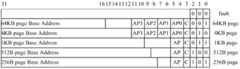
图3所示为可重构存储器结构图。包括可重构存储器控制器、tag存储阵列、data存储阵列、专用DMA等。存储体部分基于4路组关联Cache结构,最大的不同是tag存储阵列和data存储阵列可以被可重构存储器控制器控制。控制器中有一组当前配置信息寄存器current_cs_reg,其中C1-C4分别用于控制一路tag存储阵列及其对应的data存储阵列。当Ci为1时,tagi将被关闭,datai作为SPM存储部分;当Ci为0时,tagi将被打开,datai作为Cache存储部分。控制器中还有一组SPM区域寄存器,可以用于存储每个程序阶段的SPM部分与主存的映射关系。另外控制器中还设置一组上下文配置信息寄存器,是为了在程序发生相变时,能够迅速进行相变上下文的切换,使可重构存储器在最短的时间内完成存储体的重构并利用专用DMA对SPM存储部分进行快速映射。从结构图中可以看出,当将某一路配置为SPM部分时,可以减少由于tag比较逻辑带来的额外功耗,并且data部分由软件不可寻址变为软件可寻址。Figure 3 shows the structural diagram of the reconfigurable memory. Including reconfigurable memory controller, tag storage array, data storage array, dedicated DMA, etc. The storage part is based on a 4-way set-associated Cache structure, and the biggest difference is that the tag storage array and the data storage array can be controlled by a reconfigurable memory controller. There is a set of current configuration information registers current_cs_reg in the controller, where C1-C4 are used to control one tag storage array and its corresponding data storage array respectively. When Ci is 1, tagi will be turned off, and datai will be used as the SPM storage part; when Ci is 0, tagi will be turned on, and datai will be used as the Cache storage part. There is also a set of SPM area registers in the controller, which can be used to store the mapping relationship between the SPM part of each program stage and the main memory. In addition, a group of context configuration information registers are set in the controller, in order to quickly switch the phase change context when the program changes phase, so that the reconfigurable memory can complete the memory bank reconstruction in the shortest time and use the dedicated DMA performs fast mapping of parts of SPM memory. It can be seen from the structure diagram that when a certain channel is configured as the SPM part, the extra power consumption caused by the tag comparison logic can be reduced, and the data part is changed from software addressable to software addressable.
图4为相变行为图的示意图。由于程序执行存在较为明显的程序阶段性,相变行为图根据程序的阶段性特点,划分程序执行的整个过程为若干个阶段,并在不同阶段内部分别得到各自的访存行为图,并根据行为图获得可重构存储器在各个程序阶段的最佳存储配置。通过动态分配算法将每个时隙内导致Cache冲突的页以及频繁访问的页利用虚存管理的机制重定位到SPM存储部分,基于程序阶段特性的动态优化可以利用有限的片上存储资源,获得相较于固定存储结构更为可观的性能和能耗收益。Fig. 4 is a schematic diagram of a phase transition behavior diagram. Since the program execution has a relatively obvious program stage, the phase change behavior diagram divides the entire process of program execution into several stages according to the stage characteristics of the program, and obtains the respective memory access behavior diagrams in different stages, and according to the behavior The optimal storage configuration of the reconfigurable memory at each program stage is obtained from Fig. Through the dynamic allocation algorithm, the pages that cause Cache conflicts and frequently accessed pages in each time slot are relocated to the SPM storage part by using the virtual memory management mechanism. Dynamic optimization based on the characteristics of the program stage can use limited on-chip storage resources to obtain corresponding Significant performance and power gains over fixed storage structures.
图5所示为利用虚存机制对可重构片上统一存储器进行动态管理的方法的系统流程图。FIG. 5 is a system flowchart of a method for dynamically managing the reconfigurable on-chip unified memory by using a virtual memory mechanism.
在程序分析阶段,第一步将可重构处理器所有bank配置为Cache,通过收集到的Cache部分的跟踪信息,建立程序相变行为图。基于相变行为图可以实现对程序非侵入式的分析。第二步,进行数学抽象,通过对相变行为图进行数学建模以描述各指令页在程序执行过程中的访问情况以及各页之间的关系,继而通过分析不同程序阶段各指令页权重分布的变化来定量描述各备选节点的状态对能耗函数的影响,最终由整数非线性规划求得整体能耗收益最优时每个节点的状态。第三步,根据第二步的分析结果得到在每个程序阶段,所需要存储器的最佳配置,确定可重构存储器每个程序阶段的重构配置信息。第四步,根据重构后的存储结构分配,即Cache部分和SPM部分的参数,决定每个程序阶段需要映射到SPM部分的指令页页号以及在SPM部分中的区域分布,得到SPM区域寄存器组的值。在完成上述步骤后,可以得到程序执行过程中每个阶段的存储器配置信息以及SPM存储部分的区域映射关系。In the program analysis phase, the first step is to configure all banks of the reconfigurable processor as Cache, and build a program phase change behavior diagram through the collected trace information of the Cache part. Non-intrusive analysis of the program can be realized based on the phase transition behavior diagram. The second step is to carry out mathematical abstraction. Through mathematical modeling of the phase change behavior diagram to describe the access status of each instruction page during program execution and the relationship between each page, and then analyze the weight distribution of each instruction page in different program stages Quantitatively describe the influence of the state of each candidate node on the energy consumption function, and finally obtain the state of each node when the overall energy consumption benefit is optimal by integer nonlinear programming. In the third step, according to the analysis results of the second step, the optimal configuration of the required memory is obtained at each program stage, and the reconfiguration configuration information of each program stage of the reconfigurable memory is determined. The fourth step is to determine the instruction page number that needs to be mapped to the SPM part in each program stage and the area distribution in the SPM part according to the reconfigured storage structure allocation, that is, the parameters of the Cache part and the SPM part, and obtain the SPM area register group value. After the above steps are completed, the memory configuration information of each stage in the program execution process and the area mapping relationship of the SPM storage part can be obtained.
在程序执行阶段,首先将配置信息寄存器和SPM区域寄存器的值加载到可重构存储器控制器中。当程序相位发生变化时,处理器内核将接受到中断控制器发出的中断请求,然后系统进入中断模式。在中断模式下,通过加载上下文配置信息寄存器中的配置信息到当前配置信息寄存器中,完成对可重构存储器的重新配置,页表项的修改及SPM存储器中内容的换入换出,以适应当前程序阶段的程序访存模态。中断处理的具体过程为:第一步,在进入中断模式并保存相关的环境变量后,由于需要对存储器进行重新配置以及修改页表,关闭可重构存储器中的Cache部分和MMU。第二步,读取相变计数寄存器得到当前的程序阶段号。第三步,读取当前阶段区域寄存器,修改需要映射到SPM的指令页所对应的页表项。第四步,加载上下文配置信息寄存器中的配置信息到当前配置信息寄存器中,可重构存储器控制器根据当前配置信息寄存器配置存储器结构。第五步,配置专用DMA,加载映射区域寄存器中主存地址到DMA的源地址寄存器,并加载SPM存储部分对应页的物理地址到DMA的目的地址寄存器,然后使能DMA将需要映射到SPM的指令页搬运到SPM部分。第六步,DMA搬运结束后,使能Cache和MMU,并恢复中断前的环境变量,退出中断处理程序,处理器内核开始继续执行中断以前的程序。In the program execution stage, the values of the configuration information register and the SPM area register are first loaded into the reconfigurable memory controller. When the program phase changes, the processor core will receive the interrupt request from the interrupt controller, and then the system will enter the interrupt mode. In interrupt mode, by loading the configuration information in the context configuration information register to the current configuration information register, the reconfiguration of the reconfigurable memory, the modification of the page table entry and the swapping in and out of the contents of the SPM memory are completed to adapt to Program fetch mode for the current program phase. The specific process of interrupt processing is as follows: first step, after entering the interrupt mode and saving related environment variables, due to the need to reconfigure the memory and modify the page table, close the Cache part and MMU in the reconfigurable memory. The second step is to read the phase change count register to get the current program stage number. The third step is to read the current stage area register, and modify the page table entry corresponding to the instruction page that needs to be mapped to the SPM. In the fourth step, the configuration information in the context configuration information register is loaded into the current configuration information register, and the reconfigurable memory controller configures the memory structure according to the current configuration information register. The fifth step is to configure a dedicated DMA, load the main memory address in the mapping area register to the source address register of the DMA, and load the physical address of the corresponding page of the SPM storage part to the destination address register of the DMA, and then enable the DMA to be mapped to the SPM The instruction page was moved to the SPM section. Step 6: After the DMA transfer is completed, enable the Cache and MMU, restore the environment variables before the interrupt, exit the interrupt handler, and the processor core continues to execute the program before the interrupt.
Claims (6)
Translated fromChinesePriority Applications (1)
| Application Number | Priority Date | Filing Date | Title |
|---|---|---|---|
| CN2011100073102ACN102073596B (en) | 2011-01-14 | 2011-01-14 | Method for managing reconfigurable on-chip unified memory aiming at instructions |
Applications Claiming Priority (1)
| Application Number | Priority Date | Filing Date | Title |
|---|---|---|---|
| CN2011100073102ACN102073596B (en) | 2011-01-14 | 2011-01-14 | Method for managing reconfigurable on-chip unified memory aiming at instructions |
Publications (2)
| Publication Number | Publication Date |
|---|---|
| CN102073596Atrue CN102073596A (en) | 2011-05-25 |
| CN102073596B CN102073596B (en) | 2012-07-25 |
Family
ID=44032142
Family Applications (1)
| Application Number | Title | Priority Date | Filing Date |
|---|---|---|---|
| CN2011100073102AExpired - Fee RelatedCN102073596B (en) | 2011-01-14 | 2011-01-14 | Method for managing reconfigurable on-chip unified memory aiming at instructions |
Country Status (1)
| Country | Link |
|---|---|
| CN (1) | CN102073596B (en) |
Cited By (10)
| Publication number | Priority date | Publication date | Assignee | Title |
|---|---|---|---|---|
| CN102662861A (en)* | 2012-03-22 | 2012-09-12 | 北京北大众志微系统科技有限责任公司 | Software-aided inserting strategy control method for last-level cache |
| CN103207838A (en)* | 2012-01-17 | 2013-07-17 | 展讯通信(上海)有限公司 | Method for improving property of chip |
| CN103345429A (en)* | 2013-06-19 | 2013-10-09 | 中国科学院计算技术研究所 | High-concurrency access and storage accelerating method and accelerator based on on-chip RAM, and CPU |
| CN103593324A (en)* | 2013-11-12 | 2014-02-19 | 上海新储集成电路有限公司 | A fast-starting low-power computer system-on-chip with self-learning function |
| CN104067244A (en)* | 2012-01-23 | 2014-09-24 | 高通股份有限公司 | Preventing the displacement of high temporal locality of reference data fill buffers |
| CN104813286A (en)* | 2012-12-20 | 2015-07-29 | 英特尔公司 | Method, device, system for continuous automatic adjustment of code areas |
| WO2015149433A1 (en)* | 2014-03-31 | 2015-10-08 | Tsinghua University | Method and device for generating configuration information of dynamic reconfigurable processor |
| US9239786B2 (en) | 2012-01-18 | 2016-01-19 | Samsung Electronics Co., Ltd. | Reconfigurable storage device |
| CN106708747A (en)* | 2015-11-17 | 2017-05-24 | 深圳市中兴微电子技术有限公司 | Memory switching method and device |
| CN110806898A (en)* | 2019-05-22 | 2020-02-18 | 成都海光集成电路设计有限公司 | Processor and instruction operation method |
Citations (4)
| Publication number | Priority date | Publication date | Assignee | Title |
|---|---|---|---|---|
| EP1045307A2 (en)* | 1999-04-16 | 2000-10-18 | Infineon Technologies North America Corp. | Dynamic reconfiguration of a micro-controller cache memory |
| CN101739358A (en)* | 2009-12-21 | 2010-06-16 | 东南大学 | Method for dynamically allocating on-chip heterogeneous memory resources by utilizing virtual memory mechanism |
| CN101763316A (en)* | 2009-12-25 | 2010-06-30 | 东南大学 | Method for dynamically distributing isomerism storage resources on instruction parcel based on virtual memory mechanism |
| CN201540564U (en)* | 2009-12-21 | 2010-08-04 | 东南大学 | A circuit for dynamically allocating on-chip heterogeneous storage resources using the virtual memory mechanism |
- 2011
- 2011-01-14CNCN2011100073102Apatent/CN102073596B/ennot_activeExpired - Fee Related
Patent Citations (4)
| Publication number | Priority date | Publication date | Assignee | Title |
|---|---|---|---|---|
| EP1045307A2 (en)* | 1999-04-16 | 2000-10-18 | Infineon Technologies North America Corp. | Dynamic reconfiguration of a micro-controller cache memory |
| CN101739358A (en)* | 2009-12-21 | 2010-06-16 | 东南大学 | Method for dynamically allocating on-chip heterogeneous memory resources by utilizing virtual memory mechanism |
| CN201540564U (en)* | 2009-12-21 | 2010-08-04 | 东南大学 | A circuit for dynamically allocating on-chip heterogeneous storage resources using the virtual memory mechanism |
| CN101763316A (en)* | 2009-12-25 | 2010-06-30 | 东南大学 | Method for dynamically distributing isomerism storage resources on instruction parcel based on virtual memory mechanism |
Non-Patent Citations (1)
| Title |
|---|
| 《电脑知识与技术》 20090831 张阳等 利用虚存管理的思想实现基于SPM的动态能耗优化机制 第5卷, 第24期 2* |
Cited By (21)
| Publication number | Priority date | Publication date | Assignee | Title |
|---|---|---|---|---|
| CN103207838A (en)* | 2012-01-17 | 2013-07-17 | 展讯通信(上海)有限公司 | Method for improving property of chip |
| CN103207838B (en)* | 2012-01-17 | 2016-03-30 | 展讯通信(上海)有限公司 | Improve the method for chip performance |
| US9239786B2 (en) | 2012-01-18 | 2016-01-19 | Samsung Electronics Co., Ltd. | Reconfigurable storage device |
| US10114750B2 (en) | 2012-01-23 | 2018-10-30 | Qualcomm Incorporated | Preventing the displacement of high temporal locality of reference data fill buffers |
| CN104067244A (en)* | 2012-01-23 | 2014-09-24 | 高通股份有限公司 | Preventing the displacement of high temporal locality of reference data fill buffers |
| CN104067244B (en)* | 2012-01-23 | 2017-10-31 | 高通股份有限公司 | Prevent the displacement of the high temporal locality of reference data fill buffer |
| CN102662861A (en)* | 2012-03-22 | 2012-09-12 | 北京北大众志微系统科技有限责任公司 | Software-aided inserting strategy control method for last-level cache |
| CN102662861B (en)* | 2012-03-22 | 2014-12-10 | 北京北大众志微系统科技有限责任公司 | Software-aided inserting strategy control method for last-level cache |
| CN104813286B (en)* | 2012-12-20 | 2018-08-10 | 英特尔公司 | Method, device, system for continuous automatic adjustment of code areas |
| CN104813286A (en)* | 2012-12-20 | 2015-07-29 | 英特尔公司 | Method, device, system for continuous automatic adjustment of code areas |
| US9904555B2 (en) | 2012-12-20 | 2018-02-27 | Intel Corporation | Method, apparatus, system for continuous automatic tuning of code regions |
| CN108874457A (en)* | 2012-12-20 | 2018-11-23 | 英特尔公司 | Method, apparatus, the system of continuous adjust automatically for code area |
| CN108874457B (en)* | 2012-12-20 | 2021-08-17 | 英特尔公司 | Method, device and system for continuous automatic adjustment of code area |
| CN103345429B (en)* | 2013-06-19 | 2018-03-30 | 中国科学院计算技术研究所 | High concurrent memory access accelerated method, accelerator and CPU based on RAM on piece |
| CN103345429A (en)* | 2013-06-19 | 2013-10-09 | 中国科学院计算技术研究所 | High-concurrency access and storage accelerating method and accelerator based on on-chip RAM, and CPU |
| CN103593324A (en)* | 2013-11-12 | 2014-02-19 | 上海新储集成电路有限公司 | A fast-starting low-power computer system-on-chip with self-learning function |
| WO2015149433A1 (en)* | 2014-03-31 | 2015-10-08 | Tsinghua University | Method and device for generating configuration information of dynamic reconfigurable processor |
| CN106708747A (en)* | 2015-11-17 | 2017-05-24 | 深圳市中兴微电子技术有限公司 | Memory switching method and device |
| WO2017084415A1 (en)* | 2015-11-17 | 2017-05-26 | 深圳市中兴微电子技术有限公司 | Memory switching method, device, and computer storage medium |
| CN110806898A (en)* | 2019-05-22 | 2020-02-18 | 成都海光集成电路设计有限公司 | Processor and instruction operation method |
| CN110806898B (en)* | 2019-05-22 | 2021-09-14 | 成都海光集成电路设计有限公司 | Processor and instruction operation method |
Also Published As
| Publication number | Publication date |
|---|---|
| CN102073596B (en) | 2012-07-25 |
Similar Documents
| Publication | Publication Date | Title |
|---|---|---|
| CN102073596B (en) | Method for managing reconfigurable on-chip unified memory aiming at instructions | |
| CN101763316B (en) | Method for dynamic allocation of heterogeneous storage resources on instruction chip based on virtual memory mechanism | |
| CN101739358B (en) | Method for dynamically allocating on-chip heterogeneous memory resources by utilizing virtual memory mechanism | |
| US9921972B2 (en) | Method and apparatus for implementing a heterogeneous memory subsystem | |
| TWI454909B (en) | Memory device, method and system to reduce the power consumption of a memory device | |
| JP5916955B2 (en) | Method, system and device for hybrid memory management | |
| US6789172B2 (en) | Cache and DMA with a global valid bit | |
| CN108139981B (en) | Access method for page table cache TLB table entry and processing chip | |
| US6697916B2 (en) | Cache with block prefetch and DMA | |
| US6678797B2 (en) | Cache/smartcache with interruptible block prefetch | |
| CN201540564U (en) | A circuit for dynamically allocating on-chip heterogeneous storage resources using the virtual memory mechanism | |
| CN201570016U (en) | Dynamic command on-chip heterogenous memory resource distribution circuit based on virtual memory mechanism | |
| US20120151232A1 (en) | CPU in Memory Cache Architecture | |
| WO2014105163A1 (en) | Apparatus and method for implementing a scratchpad memory | |
| Jing et al. | Cache-emulated register file: An integrated on-chip memory architecture for high performance GPGPUs | |
| KR102543675B1 (en) | Configurable skewed associativity in translation lookaside buffer | |
| CN103019955A (en) | Memory management method based on application of PCRAM (phase change random access memory) main memory | |
| WO2014105151A1 (en) | Apparatus and method for a multiple page size translation lookaside buffer (tlb) | |
| KR20210158745A (en) | Flash-based coprocessor | |
| Yang et al. | HMvisor: Dynamic hybrid memory management for virtual machines | |
| CN101004715B (en) | Address translators and address translation methods | |
| Park et al. | Uvmmu: Hardware-offloaded page migration for heterogeneous computing | |
| Zhang et al. | Design and optimization of large size and low overhead off-chip caches | |
| US20140122807A1 (en) | Memory address translations | |
| Pan et al. | Lsp: Collective cross-page prefetching for nvm |
Legal Events
| Date | Code | Title | Description |
|---|---|---|---|
| C06 | Publication | ||
| PB01 | Publication | ||
| C10 | Entry into substantive examination | ||
| SE01 | Entry into force of request for substantive examination | ||
| C14 | Grant of patent or utility model | ||
| GR01 | Patent grant | ||
| CF01 | Termination of patent right due to non-payment of annual fee | Granted publication date:20120725 Termination date:20150114 | |
| EXPY | Termination of patent right or utility model |