CN102063864B - Image display and image display method - Google Patents
Image display and image display methodDownload PDFInfo
- Publication number
- CN102063864B CN102063864BCN2010105413125ACN201010541312ACN102063864BCN 102063864 BCN102063864 BCN 102063864BCN 2010105413125 ACN2010105413125 ACN 2010105413125ACN 201010541312 ACN201010541312 ACN 201010541312ACN 102063864 BCN102063864 BCN 102063864B
- Authority
- CN
- China
- Prior art keywords
- display
- image data
- still image
- display element
- viewing area
- Prior art date
- Legal status (The legal status is an assumption and is not a legal conclusion. Google has not performed a legal analysis and makes no representation as to the accuracy of the status listed.)
- Active
Links
Images


Classifications
- G—PHYSICS
- G09—EDUCATION; CRYPTOGRAPHY; DISPLAY; ADVERTISING; SEALS
- G09G—ARRANGEMENTS OR CIRCUITS FOR CONTROL OF INDICATING DEVICES USING STATIC MEANS TO PRESENT VARIABLE INFORMATION
- G09G3/00—Control arrangements or circuits, of interest only in connection with visual indicators other than cathode-ray tubes
- G09G3/20—Control arrangements or circuits, of interest only in connection with visual indicators other than cathode-ray tubes for presentation of an assembly of a number of characters, e.g. a page, by composing the assembly by combination of individual elements arranged in a matrix no fixed position being assigned to or needed to be assigned to the individual characters or partial characters
- G09G3/22—Control arrangements or circuits, of interest only in connection with visual indicators other than cathode-ray tubes for presentation of an assembly of a number of characters, e.g. a page, by composing the assembly by combination of individual elements arranged in a matrix no fixed position being assigned to or needed to be assigned to the individual characters or partial characters using controlled light sources
- G09G3/30—Control arrangements or circuits, of interest only in connection with visual indicators other than cathode-ray tubes for presentation of an assembly of a number of characters, e.g. a page, by composing the assembly by combination of individual elements arranged in a matrix no fixed position being assigned to or needed to be assigned to the individual characters or partial characters using controlled light sources using electroluminescent panels
- G09G3/32—Control arrangements or circuits, of interest only in connection with visual indicators other than cathode-ray tubes for presentation of an assembly of a number of characters, e.g. a page, by composing the assembly by combination of individual elements arranged in a matrix no fixed position being assigned to or needed to be assigned to the individual characters or partial characters using controlled light sources using electroluminescent panels semiconductive, e.g. using light-emitting diodes [LED]
- G09G3/3208—Control arrangements or circuits, of interest only in connection with visual indicators other than cathode-ray tubes for presentation of an assembly of a number of characters, e.g. a page, by composing the assembly by combination of individual elements arranged in a matrix no fixed position being assigned to or needed to be assigned to the individual characters or partial characters using controlled light sources using electroluminescent panels semiconductive, e.g. using light-emitting diodes [LED] organic, e.g. using organic light-emitting diodes [OLED]
- G09G3/3225—Control arrangements or circuits, of interest only in connection with visual indicators other than cathode-ray tubes for presentation of an assembly of a number of characters, e.g. a page, by composing the assembly by combination of individual elements arranged in a matrix no fixed position being assigned to or needed to be assigned to the individual characters or partial characters using controlled light sources using electroluminescent panels semiconductive, e.g. using light-emitting diodes [LED] organic, e.g. using organic light-emitting diodes [OLED] using an active matrix
- G09G3/3233—Control arrangements or circuits, of interest only in connection with visual indicators other than cathode-ray tubes for presentation of an assembly of a number of characters, e.g. a page, by composing the assembly by combination of individual elements arranged in a matrix no fixed position being assigned to or needed to be assigned to the individual characters or partial characters using controlled light sources using electroluminescent panels semiconductive, e.g. using light-emitting diodes [LED] organic, e.g. using organic light-emitting diodes [OLED] using an active matrix with pixel circuitry controlling the current through the light-emitting element
- G—PHYSICS
- G09—EDUCATION; CRYPTOGRAPHY; DISPLAY; ADVERTISING; SEALS
- G09G—ARRANGEMENTS OR CIRCUITS FOR CONTROL OF INDICATING DEVICES USING STATIC MEANS TO PRESENT VARIABLE INFORMATION
- G09G2300/00—Aspects of the constitution of display devices
- G09G2300/08—Active matrix structure, i.e. with use of active elements, inclusive of non-linear two terminal elements, in the pixels together with light emitting or modulating elements
- G09G2300/0809—Several active elements per pixel in active matrix panels
- G09G2300/0842—Several active elements per pixel in active matrix panels forming a memory circuit, e.g. a dynamic memory with one capacitor
- G—PHYSICS
- G09—EDUCATION; CRYPTOGRAPHY; DISPLAY; ADVERTISING; SEALS
- G09G—ARRANGEMENTS OR CIRCUITS FOR CONTROL OF INDICATING DEVICES USING STATIC MEANS TO PRESENT VARIABLE INFORMATION
- G09G2320/00—Control of display operating conditions
- G09G2320/04—Maintaining the quality of display appearance
- G09G2320/043—Preventing or counteracting the effects of ageing
- G09G2320/046—Dealing with screen burn-in prevention or compensation of the effects thereof
- G—PHYSICS
- G09—EDUCATION; CRYPTOGRAPHY; DISPLAY; ADVERTISING; SEALS
- G09G—ARRANGEMENTS OR CIRCUITS FOR CONTROL OF INDICATING DEVICES USING STATIC MEANS TO PRESENT VARIABLE INFORMATION
- G09G2320/00—Control of display operating conditions
- G09G2320/04—Maintaining the quality of display appearance
- G09G2320/043—Preventing or counteracting the effects of ageing
- G09G2320/048—Preventing or counteracting the effects of ageing using evaluation of the usage time
- G—PHYSICS
- G09—EDUCATION; CRYPTOGRAPHY; DISPLAY; ADVERTISING; SEALS
- G09G—ARRANGEMENTS OR CIRCUITS FOR CONTROL OF INDICATING DEVICES USING STATIC MEANS TO PRESENT VARIABLE INFORMATION
- G09G2320/00—Control of display operating conditions
- G09G2320/06—Adjustment of display parameters
- G09G2320/0613—The adjustment depending on the type of the information to be displayed
- G—PHYSICS
- G09—EDUCATION; CRYPTOGRAPHY; DISPLAY; ADVERTISING; SEALS
- G09G—ARRANGEMENTS OR CIRCUITS FOR CONTROL OF INDICATING DEVICES USING STATIC MEANS TO PRESENT VARIABLE INFORMATION
- G09G2320/00—Control of display operating conditions
- G09G2320/10—Special adaptations of display systems for operation with variable images
- G09G2320/103—Detection of image changes, e.g. determination of an index representative of the image change
Landscapes
- Engineering & Computer Science (AREA)
- Physics & Mathematics (AREA)
- Computer Hardware Design (AREA)
- General Physics & Mathematics (AREA)
- Theoretical Computer Science (AREA)
- Control Of Indicators Other Than Cathode Ray Tubes (AREA)
- Control Of El Displays (AREA)
- Electroluminescent Light Sources (AREA)
Abstract
Translated fromChinese
Description
Translated fromChinese技术领域technical field
本发明涉及图像显示器和图像显示方法,该图像显示器通过驱动例如诸如有机EL(电致发光)元件之类的自发光元件来显示图像。The present invention relates to an image display that displays an image by driving, for example, a self-luminous element such as an organic EL (Electro Luminescence) element, and an image display method.
背景技术Background technique
近年来,在显示图像的显示器的领域中,使用电流驱动型光学元件(例如,有机EL(电致发光)元件)作为像素的发光元件的显示器已被开发出来进入商业化,这种电流驱动型光学元件的发光亮度根据流经其的电流值而改变。与液晶元件等不同,有机EL元件是自发光元件。因此,在使用有机EL元件的显示器(有机EL显示器)中,光源(背光)不是必需的,因此与需要光源的液晶显示器相比,可减小显示器的轮廓并增大显示器的亮度。具体而言,在显示器使用有源矩阵系统作为驱动系统的情况下,每个像素被允许连续地发光,并且可实现功耗的降低。因此,有机EL显示器被预期成为下一代平板显示器的主流。In recent years, in the field of displays for displaying images, displays using current-driven optical elements (for example, organic EL (electroluminescent) elements) as light-emitting elements of pixels have been developed and commercialized. The light emission brightness of the optical element changes according to the value of the current flowing therethrough. Unlike liquid crystal elements and the like, organic EL elements are self-luminous elements. Therefore, in a display using an organic EL element (organic EL display), a light source (backlight) is not necessary, so that the profile of the display can be reduced and the brightness of the display can be increased compared to a liquid crystal display that requires a light source. Specifically, in the case of a display using an active matrix system as a driving system, each pixel is allowed to emit light continuously, and reduction in power consumption can be achieved. Therefore, organic EL displays are expected to become the mainstream of next-generation flat panel displays.
有机EL元件是电流驱动型发光元件,并且是能够通过控制流经其的电流的量来调节灰度(gradation)的元件。然而,有机EL元件具有根据其发光量和其通电时间而劣化(degrade)的特性,并且在劣化的后期阶段中有机EL元件的亮度相比于在劣化的早期阶段中有机EL元件的亮度会相对地下降。另一方面,所显示的图像的亮度在所有像素中并不是均匀的,因此在所有像素中有机EL元件的劣化也是不均匀的。因此,在显示区域中发生有机EL元件中根据劣化度的亮度下降。The organic EL element is a current-driven light emitting element, and is an element capable of adjusting gradation by controlling the amount of current flowing therethrough. However, the organic EL element has a characteristic of degrading according to its light emission amount and its energization time, and the luminance of the organic EL element in the later stage of degradation will be relatively lower than that in the early stage of degradation. down. On the other hand, the luminance of a displayed image is not uniform in all pixels, and thus the degradation of the organic EL element is not uniform in all pixels. Therefore, a decrease in luminance according to the degree of deterioration in the organic EL element occurs in the display region.
该现象被称为“老化”(burn-in),具体而言,当静止图像被长时间显示在显示屏上时,容易发生老化。为了准确地校正“老化”,有必要正确地检测有机EL元件的实际劣化状态。作为对该问题的一种解决方案,例如,已报告了大量的利用从累积发光时间得出的每个像素的劣化量来校正影像信号(picture signal)的方法,例如在日本未实审专利申请公布No.2007-206463中描述的方法。This phenomenon is called "burn-in", and specifically, when a still image is displayed on a display screen for a long time, burn-in tends to occur. In order to correct "aging" accurately, it is necessary to correctly detect the actual state of deterioration of the organic EL element. As a solution to this problem, for example, a large number of methods of correcting a picture signal using the degradation amount of each pixel derived from the cumulative luminescence time have been reported, for example, in Japanese Unexamined Patent Application The method described in Publication No. 2007-206463.
发明内容Contents of the invention
然而,在日本未实审专利申请公布No.2007-206463描述的显示器中,影像信号在任意时刻被从外部输入,因此难以预测要输入的影像信号。因此,有必要实时地对累积显示时间进行计数。此外,难以预先得出对影像信号的校正量,因此有必要实时地得出校正量。结果是系统变大。However, in the display described in Japanese Unexamined Patent Application Publication No. 2007-206463, a video signal is input from the outside at an arbitrary timing, and thus it is difficult to predict a video signal to be input. Therefore, it is necessary to count the cumulative display time in real time. In addition, it is difficult to obtain the correction amount for the video signal in advance, so it is necessary to obtain the correction amount in real time. The result is that the system becomes larger.
希望提供一种能够利用简单系统来减轻老化的图像显示器和图像显示方法。It is desirable to provide an image display and an image display method capable of reducing burn-in with a simple system.
根据本发明的一个实施例,提供了一种图像显示器,包括显示面板和存储器部件,显示面板包括显示区域,在显示区域中,分别包括自发光型第一显示元件的多个像素被二维地布置,存储器部件存储第一显示元件的劣化特性数据。图像显示器还包括驱动部件。驱动部件根据从外部输入的多个静止图像数据和基于多个静止图像数据的多个静止图像在显示区域上的显示时间,来得出当多个静止图像被顺序地逐个显示在显示区域上时每个静止图像数据中每个第一显示元件的累积显示时间。驱动部件还根据在每个静止图像数据中得出的每个第一显示元件的累积显示时间和劣化特性数据来得出每个像素中每个静止图像数据的校正量,并进一步在显示区域上顺序地逐个显示基于利用所获得的校正量校正了的多个静止图像数据的多个静止图像。According to one embodiment of the present invention, there is provided an image display including a display panel and a memory component, the display panel includes a display area, and in the display area, a plurality of pixels respectively including self-luminous first display elements are two-dimensionally Arranged, the memory section stores degradation characteristic data of the first display element. The image display also includes drive components. The driving part derives, based on the plurality of still image data input from the outside and the display time of the plurality of still images based on the plurality of still image data on the display area, to obtain when the plurality of still images are sequentially displayed on the display area one by one. The cumulative display time of each first display element in the still image data. The drive section also derives the correction amount of each still image data in each pixel based on the accumulated display time and degradation characteristic data of each first display element obtained in each still image data, and further sequentially A plurality of still images based on the plurality of still image data corrected with the obtained correction amount is displayed one by one.
根据本发明的一个实施例,提供了一种包括显示区域的图像显示器中的图像显示方法,在显示区域中,分别包括自发光型第一显示元件的多个像素被二维地布置,该方法包括以下三个步骤:According to one embodiment of the present invention, there is provided an image display method in an image display including a display area in which a plurality of pixels respectively including self-luminous first display elements are two-dimensionally arranged, the method Include the following three steps:
(1)根据从外部输入的多个静止图像数据和基于多个静止图像数据的多个静止图像在显示区域上的显示时间,来得出当多个静止图像被顺序地逐个显示在显示区域上时每个静止图像数据中每个第一显示元件的累积显示时间;(1) According to the display time on the display area of a plurality of still image data input from the outside and a plurality of still images based on the plurality of still image data, when a plurality of still images are sequentially displayed on the display area one by one cumulative display time for each first display element in each still image data;
(2)根据在每个静止图像数据中得出的每个第一显示元件的累积显示时间和劣化特性数据,来得出每个像素中每个静止图像数据的校正量;以及(2) obtaining the correction amount of each still image data in each pixel based on the cumulative display time and degradation characteristic data of each first display element obtained in each still image data; and
(3)进一步在显示区域上顺序地逐个显示基于利用所获得的校正量校正了的多个静止图像数据的多个静止图像。(3) A plurality of still images based on the plurality of still image data corrected with the obtained correction amount is further sequentially displayed one by one on the display area.
在根据本发明实施例的图像显示器和图像显示方法中,用于图像显示的多个静止图像数据和基于多个静止图像数据的多个静止图像的显示时间在图像显示之前是已知的。因此,每个第一显示元件的累积显示时间(即,劣化量)可以被估计,从而使得每个静止图像数据的每个显示像素的校正量在图像显示之前可以被确定。In an image display and an image display method according to an embodiment of the present invention, a plurality of still image data for image display and display times of a plurality of still images based on the plurality of still image data are known before image display. Accordingly, the cumulative display time (ie, degradation amount) of each first display element can be estimated, so that the correction amount of each display pixel of each still image data can be determined before image display.
在根据本发明实施例的图像显示器和图像显示方法中,分别包括自发光型第二显示元件的一个或多个伪像素和检测从这一个或多个伪像素发出的光的光传感器可以被布置在非显示区域中。在这种情况下,可使得利用从光传感器输出的光检测信号来校正劣化特性数据。In an image display and an image display method according to an embodiment of the present invention, one or more dummy pixels each including a self-luminous type second display element and a photosensor for detecting light emitted from the one or more dummy pixels may be arranged in the non-display area. In this case, the degradation characteristic data may be corrected using the light detection signal output from the light sensor.
在根据本发明实施例的图像显示器和图像显示方法中,对从外部输入的每个静止图像数据中每个像素的校正量在图像显示之前被确定。因此,没有必要实时地对累积显示时间进行计数或者实时地得出校正量,从而使得可利用简单的系统来减轻老化。In the image display and image display method according to the embodiment of the present invention, the correction amount for each pixel in each still image data input from the outside is determined before image display. Therefore, it is not necessary to count the accumulated display time in real time or derive the correction amount in real time, making it possible to reduce burn-in with a simple system.
本发明的其他和进一步的目的、特征和优点将更完整地表现在下面的描述中。Other and further objects, features and advantages of the invention will appear more fully in the following description.
附图说明Description of drawings
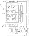
图1是根据本发明一个实施例的显示器的示意性配置图。FIG. 1 is a schematic configuration diagram of a display according to one embodiment of the present invention.
图2是图1中显示区域的配置图。FIG. 2 is a configuration diagram of a display area in FIG. 1 .
图3是图1中显示器的修改例的示意性配置图。FIG. 3 is a schematic configuration diagram of a modification example of the display in FIG. 1 .
具体实施方式Detailed ways
下面将参考附图详细描述优选实施例。将按以下顺序给出描述。Preferred embodiments will be described in detail below with reference to the accompanying drawings. Description will be given in the following order.
1.实施例(参考图1和2)1. Embodiment (with reference to Fig. 1 and 2)
2.修改例(参考图3)2. Modified example (refer to Figure 3)
实施例Example
显示器1的示意性配置Schematic Configuration of Display 1
图1图示了根据本发明一个实施例的显示器1的示意性配置。例如,显示器1可适合用作静止图像的显示器,其在画面中顺序地逐个显示多个静止图像。显示器1例如包括显示面板10和驱动显示面板10的驱动电路20(驱动部件)。FIG. 1 illustrates a schematic configuration of a display 1 according to one embodiment of the present invention. For example, the display 1 can be suitably used as a still image display that sequentially displays a plurality of still images one by one in a screen. The display 1 includes, for example, a
显示面板10包括显示区域10A,其中发出彼此不同颜色的三种有机EL元件11R、11G和11B(自发光型的第一显示元件)被二维地布置。显示区域10A是利用从有机EL元件11R、11G和11B发出的光来显示影像的区域。有机EL元件11R、11G和11B是分别发出红光、绿光和蓝光的有机EL元件。下文中,有机EL元件11R、11G和11B在必要时被总称为有机EL元件11。The
显示像素15
图2图示了显示区域10A中的电路配置的示例。在显示区域10A中,多个像素电路13被二维地布置以便分别与有机EL元件11成对。在实施例中,有机EL元件11和像素电路13的对构成一个子像素14。更具体而言,如图1和3所示,一对有机EL元件11R和像素电路13构成一个子像素14R,一对有机EL元件11G和像素电路13构成一个子像素14G,一对有机EL元件11B和像素电路13构成一个子像素14B。此外,三个相邻的子像素14R、14G和14B构成一个像素(一个显示像素15)。FIG. 2 illustrates an example of a circuit configuration in the
每个像素电路13例如由驱动晶体管Tr1、写入晶体管Tr2和保持电容器CS构成,即,每个像素电路13具有2Tr1C的电路配置。驱动晶体管Tr1和写入晶体管Tr2各自例如由n沟道MOS型薄膜晶体管(TFT)构成。驱动晶体管Tr1或写入晶体管Tr2可以例如由p沟道MOS型TFT构成。Each
在显示区域10A中,多条信号线DTL被布置在列方向上,并且多条扫描线WSL和多条电源线PSL(提供电源电压的构件)被布置在行方向上。一个有机EL元件11被布置在信号线DTL和扫描线WSL的每个交点周围。每条信号线DTL连接到信号线驱动电路23(将在后面描述)的输出端(未示出)以及写入晶体管Tr2的漏电极和源电极(两者都未示出)中的一者。每条扫描线WSL连接到扫描线驱动电路24(将在后面描述)的输出端和写入晶体管Tr2的栅电极(未示出)。每条电源线PSL连接到电源线驱动电路25(将在后面描述)的输出端(未示出)以及驱动晶体管Tr1的漏电极和源电极(两者都未示出)中的一者。写入晶体管Tr2的漏电极和源电极中未连接到信号线DTL的一者(未示出)连接到驱动晶体管Tr1的栅电极和保持电容器CS的一端。驱动晶体管Tr1的漏电极和源电极中未连接到电源线PSL的一者(未示出)和保持电容器CS的另一端连接到有机EL元件11的阳极电极(未示出)。有机EL元件11的阴极电极(未示出)例如连接到地线GND。In the
驱动电路20
接下来,将参考图1描述驱动电路20中的每个电路。驱动电路20包括定时生成电路21、图像处理电路22、信号线驱动电路23、写入线驱动电路24、电源线驱动电路25、内部存储器部件26和外部存储器部件27。Next, each circuit in the
内部存储器部件26预先存储例如有机EL元件11的劣化特性数据。劣化特性数据表示有机EL元件11的累积显示时间和对劣化数据的校正量(例如,校正系数)之间的关系。这里,累积显示时间例如是通过将有机EL元件11的发光时间和灰度数据彼此相乘而获得的值。累积显示时间可以是通过将灰度数据、有机EL元件11的发光时间和灰度系数彼此相乘而获得的值。在累积显示时间在后面将描述的校正处理中被得出的情况下,内部存储器部件26被允许进一步存储每个显示像素15(更精确地说,每个子像素14)的累积显示时间(将在后面描述)。The
外部存储器部件27可从显示器1移除,并且例如是诸如“记忆棒(MEMORY STICK,索尼公司的注册商标)”之类的典型的记录介质。在外部存储器部件27中,多个静止图像数据被预先存储。存储在外部存储器部件27中的每个静止图像数据27A被用于显示器1中的图像显示,并且例如是数字数据,该数字数据包括与显示区域10A中的每个子像素14相对应的灰度数据。The
定时生成电路21控制图像处理电路22、信号线驱动电路23、写入线驱动电路24和电源线驱动电路25彼此同步地进行操作。定时生成电路21响应于例如从系统控制部件(未示出)输出的同步信号20B(与该信号同步地)而向上述电路中的每一个输出控制信号21A。The
图像处理电路22读出例如存储在外部存储器部件27中的多个静止图像数据27A以对每个静止图像数据27A执行预定的校正处理。图像处理电路22例如在将外部存储器部件27连接到显示器1时开始上述校正处理。校正处理将在后面详细描述。此外,图像处理电路22响应于控制信号21A的输入(与其同步地)从内部存储器部件26读出通过校正处理获得的校正量(例如,Cn(x,y),这将在后面描述),然后图像处理电路22利用所读出的校正量来校正每个静止图像数据27A。接下来,图像处理电路22将通过校正获得的每个静止图像数据22A(未示出)作为影像信号22B输出到信号线驱动电路23。此时,图像处理电路22响应于控制信号21A的输入(与其同步地)将影像信号22B输出到信号线驱动电路23,以使得基于多个静止图像数据27A的多个静止图像被顺序地逐个显示。The
信号线驱动电路23响应于控制信号21A的输入(与其同步地)将从图像处理电路22输入的影像信号22B输出到每条信号线DTL以便驱动每个显示像素15。信号线驱动电路23将与写入线驱动电路24所选的一条线中的显示像素相对应的信号电压输出到与显示像素15相对应的信号线DTL。The signal
写入线驱动电路24响应于控制信号21A的输入(与其同步地)从多条扫描线WSL中选择一条扫描线WSL。电源线驱动电路25响应于控制信号21A的输入(与其同步地)向多条电源线PSL顺序地施加从电源电路(未示出)提供来的电源电压,以便控制有机EL元件11的发光和熄灭。The write
校正处理Correction process
接下来,下面将描述上述校正处理。首先,图像处理电路22根据多个静止图像数据27A和基于多个静止图像数据27A的多个静止图像向显示区域10A的显示时间,来得出当多个静止图像被顺序地逐个显示在显示区域10A上时每个显示像素15(每个有机EL元件11)在每个静止图像数据27A中的累积显示时间。Next, the above-mentioned correction processing will be described below. First, the
在这种情况下,例如,每个静止图像数据27A中包括的灰度数据是Kn(x,y)(其中n是图像显示顺序,x是x坐标值,y是y坐标值),并且显示时间是ΔTn,灰度系数是αn,累积显示时间是Tn(x,y),并且存储在外部存储器部件27中的静止图像数据27A的个数是N。此时,例如,图像处理电路22利用下面的数学式1来得出累积显示时间Tn(x,y)。In this case, for example, the gradation data included in each
数学式1Mathematical formula 1
接下来,图像处理电路22根据在每个静止图像数据27A中得出的每个显示像素15的累积显示时间和劣化特性数据,来得出对每个显示像素15中包括在每个静止图像数据27A中的灰度数据的校正量。更具体而言,图像处理电路22从劣化特性数据中提取出与在每个静止图像数据27A中得出的每个显示像素15的累积显示时间相对应的校正量。例如,图像处理电路22从劣化特性数据中提取出与累积显示时间Tn(x,y)相对应的校正量Cn(x,y)。接下来,图像处理电路22将所获得的校正量存储在内部存储器部件26中以便将校正量与每个静止图像数据27A相关联。例如,图像处理电路22将校正量Cn(x,y)存储在内部存储器部件26中。Next, the
显示器1的操作Operation of Display 1
接下来,下面将描述根据实施例的显示器1的操作示例。首先,外部存储器部件27连接到显示器1。然后,由图像处理电路22得出校正量以便存储在内部存储器部件26中。之后,控制信号21A被从定时生成电路21输出到驱动电路20中的每个电路,以使得驱动电路20中的每个电路响应于控制信号21A的指示而操作。更具体而言,在图像处理电路22中,每个静止图像数据22A被生成,并且每个生成的静止图像数据22A作为影像信号22B被信号线驱动电路23输出到每条信号线DTL,并且同时,一条扫描线WSL被写入线驱动电路24从多条扫描线WSL中顺序选择。此外,期望的电源电压被电源线驱动电路25顺序施加到多条电源线PSL。因此,每个显示像素15被驱动,并且基于多个静止图像数据27A的多个静止图像被顺序地逐个显示在显示区域10A上。Next, an operation example of the display 1 according to the embodiment will be described below. First, the
显示器1的效果The effect of display 1
接下来,下面将描述根据实施例的显示器1的效果。在实施例中,用于图像显示的所有静止图像数据27A都存储在外部存储器部件27中,并且基于所有的静止图像数据27A的所有静止图像的显示时间都是预定的。换句话说,用于图像显示的所有静止图像数据27A和基于所有静止图像数据27A的所有静止图像的显示时间在图像显示之前都是已知的。因此,每个显示像素15的累积显示时间(即,劣化量)可以被估计,从而使得每个静止图像数据27A的每个显示像素15的校正量在图像显示之前可以被确定。因此,没有必要实时地对累积显示时间进行计数或者实时地得出校正量,从而使得可利用简单的系统来减轻老化。Next, effects of the display 1 according to the embodiment will be described below. In the embodiment, all still image
修改例Modification
虽然在上述实施例中,在图像显示之前只有对每个静止图像数据27A的校正量被得出以便存储在内部存储器部件26中,但是,例如,通过校正获得的每个静止图像数据22A可以被存储在内部存储器部件26中来代替校正量或者与校正量一起存储。Although in the above-described embodiment, only the correction amount for each
此外,虽然在上述实施例中,存储在内部存储器部件26中的劣化特性数据是固定值,但是劣化特性数据在必要时可以被校正或更新。因此,可使得对每个静止图像数据27A的每个显示像素15的校正量被更准确地确定,从而使得可进一步减轻老化。Furthermore, although in the above-described embodiment, the degradation characteristic data stored in the
为了校正或更新劣化特性数据,显示器1优选地具有以下配置。例如,如图3所示,显示面板10在非显示区域10B中包括一个或多个伪像素18(包括有机EL元件12和像素电路16)和检测从这一个或多个伪像素18发出的光的光传感器19。此外,图像处理电路22为伪像素18生成标准灰度影像信号22B以将影像信号22B输出到信号线驱动电路23。信号线驱动电路23将从图像处理电路22输入的标准灰度影像信号22B输出到用于伪像素18的多条信号线DTL以驱动伪像素18。另外,图像处理电路22利用从光传感器19输出的光检测信号来校正劣化特性数据。因而,可使得通过测量亮度劣化来适当地校正劣化特性数据。In order to correct or update the deterioration characteristic data, the display 1 preferably has the following configuration. For example, as shown in FIG. 3 , the
本申请包含与2009年11月17日向日本专利局提交的日本优先专利申请JP 2009-262251中公开的内容有关的主题,该申请的全部内容通过引用结合于此。The present application contains subject matter related to that disclosed in Japanese Priority Patent Application JP 2009-262251 filed in the Japan Patent Office on November 17, 2009, the entire content of which is hereby incorporated by reference.
本领域的技术人员应当明白,可以根据设计要求和其它因素进行各种修改、组合、子组合和变更,只要它们在权利要求或其等同物的范围之内。It should be understood by those skilled in the art that various modifications, combinations, sub-combinations and alterations may occur depending on design requirements and other factors insofar as they are within the scope of the claims or the equivalents thereof.
Claims (5)
Applications Claiming Priority (2)
| Application Number | Priority Date | Filing Date | Title |
|---|---|---|---|
| JP2009262251AJP2011107410A (en) | 2009-11-17 | 2009-11-17 | Image display device and image display method |
| JP2009-262251 | 2009-11-17 |
Publications (2)
| Publication Number | Publication Date |
|---|---|
| CN102063864A CN102063864A (en) | 2011-05-18 |
| CN102063864Btrue CN102063864B (en) | 2013-12-11 |
Family
ID=43999122
Family Applications (1)
| Application Number | Title | Priority Date | Filing Date |
|---|---|---|---|
| CN2010105413125AActiveCN102063864B (en) | 2009-11-17 | 2010-11-10 | Image display and image display method |
Country Status (3)
| Country | Link |
|---|---|
| US (1) | US9001099B2 (en) |
| JP (1) | JP2011107410A (en) |
| CN (1) | CN102063864B (en) |
Families Citing this family (7)
| Publication number | Priority date | Publication date | Assignee | Title |
|---|---|---|---|---|
| JP2013057912A (en)* | 2011-09-09 | 2013-03-28 | Canon Inc | Display device and display method |
| CN104658469B (en)* | 2013-11-21 | 2017-09-22 | 奇景光电股份有限公司 | Organic light emitting display device and driving method thereof |
| KR102658426B1 (en)* | 2016-05-31 | 2024-04-17 | 엘지디스플레이 주식회사 | Organic Light Emitting Display And Driving Method Thereof |
| KR102561188B1 (en)* | 2016-09-22 | 2023-07-28 | 삼성디스플레이 주식회사 | Display Device |
| JP7391552B2 (en)* | 2019-06-27 | 2023-12-05 | エルジー ディスプレイ カンパニー リミテッド | Display control device and display control method |
| KR102708366B1 (en)* | 2019-07-30 | 2024-09-20 | 엘지전자 주식회사 | Display device and method |
| CN115223501B (en)* | 2022-08-19 | 2023-08-04 | 惠科股份有限公司 | Drive compensation circuit, compensation method and display device |
Citations (2)
| Publication number | Priority date | Publication date | Assignee | Title |
|---|---|---|---|---|
| CN1448907A (en)* | 2002-03-29 | 2003-10-15 | 东北先锋公司 | Method for aging display device and electronic apparatus using same |
| CN1682267A (en)* | 2002-09-16 | 2005-10-12 | 皇家飞利浦电子股份有限公司 | Display device |
Family Cites Families (13)
| Publication number | Priority date | Publication date | Assignee | Title |
|---|---|---|---|---|
| US5504504A (en)* | 1994-07-13 | 1996-04-02 | Texas Instruments Incorporated | Method of reducing the visual impact of defects present in a spatial light modulator display |
| US6414661B1 (en)* | 2000-02-22 | 2002-07-02 | Sarnoff Corporation | Method and apparatus for calibrating display devices and automatically compensating for loss in their efficiency over time |
| WO2001069584A1 (en)* | 2000-03-14 | 2001-09-20 | Mitsubishi Denki Kabushiki Kaisha | Image display and image displaying method |
| JP2002112169A (en)* | 2000-09-28 | 2002-04-12 | Minolta Co Ltd | Image processing unit, image processing method and recording medium with recorded image processing program |
| US6657621B2 (en)* | 2001-05-01 | 2003-12-02 | Hewlett-Packard Development Company, L.P. | Device and method for scrolling stored images across a display |
| AU2003211470A1 (en)* | 2002-03-04 | 2003-09-16 | Sanyo Electric Co., Ltd. | Organic electroluminescence display and its application |
| US20060061292A1 (en)* | 2004-09-17 | 2006-03-23 | Samsung Electronics Co., Ltd. | Display device and driving method thereof |
| JP4934963B2 (en)* | 2005-01-21 | 2012-05-23 | ソニー株式会社 | Burn-in phenomenon correction method, self-luminous device, burn-in phenomenon correction apparatus, and program |
| JP2007206463A (en) | 2006-02-02 | 2007-08-16 | Sony Corp | Self-luminous display device, input display data correction device, and program |
| KR100840102B1 (en)* | 2007-02-23 | 2008-06-19 | 삼성에스디아이 주식회사 | Organic electroluminescent display |
| TW200912848A (en)* | 2007-04-26 | 2009-03-16 | Sony Corp | Display correction circuit of organic EL panel |
| KR20080101700A (en)* | 2007-05-18 | 2008-11-21 | 소니 가부시끼 가이샤 | Display device, method of driving display device and computer program |
| JP4946795B2 (en)* | 2007-10-29 | 2012-06-06 | ソニー株式会社 | Image processing apparatus and image processing method |
- 2009
- 2009-11-17JPJP2009262251Apatent/JP2011107410A/enactivePending
- 2010
- 2010-11-10USUS12/943,518patent/US9001099B2/enactiveActive
- 2010-11-10CNCN2010105413125Apatent/CN102063864B/enactiveActive
Patent Citations (2)
| Publication number | Priority date | Publication date | Assignee | Title |
|---|---|---|---|---|
| CN1448907A (en)* | 2002-03-29 | 2003-10-15 | 东北先锋公司 | Method for aging display device and electronic apparatus using same |
| CN1682267A (en)* | 2002-09-16 | 2005-10-12 | 皇家飞利浦电子股份有限公司 | Display device |
Also Published As
| Publication number | Publication date |
|---|---|
| JP2011107410A (en) | 2011-06-02 |
| US20110115773A1 (en) | 2011-05-19 |
| US9001099B2 (en) | 2015-04-07 |
| CN102063864A (en) | 2011-05-18 |
Similar Documents
| Publication | Publication Date | Title |
|---|---|---|
| US11380246B2 (en) | Electroluminescent display device having pixel driving | |
| TWI550576B (en) | Organic light emitting display with pixel and method of driving the same | |
| CN100433108C (en) | Pixel circuit, display and driving method thereof | |
| CN102063864B (en) | Image display and image display method | |
| KR101374443B1 (en) | Organic Light Emitting Diode Display | |
| US10854123B2 (en) | Organic light emitting diode display device | |
| KR102701054B1 (en) | Driving method for display device and display device drived thereby | |
| JPWO2010146707A1 (en) | Active matrix organic EL display device and driving method thereof | |
| JP2015225150A (en) | Display device and electronic apparatus | |
| TW201329940A (en) | Color display device | |
| US20080246701A1 (en) | Organic light emitting display and its driving method | |
| CN101359449A (en) | Organic light emitting display and driving method thereof | |
| KR20110071114A (en) | Display Device Compensates for Changes in Pixel Transistor Mobility | |
| CN111883035B (en) | Display device and driving method thereof | |
| KR101971399B1 (en) | Control apparatus of display panel, display apparatus and method of driving display panel | |
| US8154482B2 (en) | Organic light emitting display and method for driving the same | |
| WO2018205717A1 (en) | Compensation method and compensation device for organic electroluminescence display and display device | |
| KR102182382B1 (en) | Organic light emitting diode display and method of driving the same | |
| JP2015197473A (en) | Signal processing method, display device, and electronic apparatus | |
| US20080252567A1 (en) | Active Matrix Display Device | |
| KR102407490B1 (en) | Light Emitting Display Device and Driving Method thereof | |
| JP2011191620A (en) | Display device and display driving method | |
| JP2011128443A (en) | Display device, method of driving the same, and electronic equipment | |
| JP2010101926A (en) | Image display device and method for driving the same | |
| JP2005321684A (en) | Video display apparatus and video display method |
Legal Events
| Date | Code | Title | Description |
|---|---|---|---|
| C06 | Publication | ||
| PB01 | Publication | ||
| C10 | Entry into substantive examination | ||
| SE01 | Entry into force of request for substantive examination | ||
| C14 | Grant of patent or utility model | ||
| GR01 | Patent grant | ||
| ASS | Succession or assignment of patent right | Owner name:JANPAN ORGANIC RATE DISPLAY CO., LTD. Free format text:FORMER OWNER: SONY CORP Effective date:20150814 | |
| C41 | Transfer of patent application or patent right or utility model | ||
| TR01 | Transfer of patent right | Effective date of registration:20150814 Address after:Tokyo, Japan Patentee after:JOLED Inc. Address before:Tokyo, Japan Patentee before:Sony Corp. | |
| TR01 | Transfer of patent right | Effective date of registration:20231225 Address after:Tokyo, Japan Patentee after:Japan Display Design and Development Contract Society Address before:Tokyo, Japan Patentee before:JOLED Inc. | |
| TR01 | Transfer of patent right | ||
| TR01 | Transfer of patent right | Effective date of registration:20250730 Address after:Tokyo, Japan Patentee after:Magno Bolan Co.,Ltd. Country or region after:Japan Address before:Tokyo, Japan Patentee before:Japan Display Design and Development Contract Society Country or region before:Japan | |
| TR01 | Transfer of patent right |