CN102054873B - Display and its thin film transistor array substrate and thin film transistor - Google Patents
Display and its thin film transistor array substrate and thin film transistorDownload PDFInfo
- Publication number
- CN102054873B CN102054873BCN200910209686.4ACN200910209686ACN102054873BCN 102054873 BCN102054873 BCN 102054873BCN 200910209686 ACN200910209686 ACN 200910209686ACN 102054873 BCN102054873 BCN 102054873B
- Authority
- CN
- China
- Prior art keywords
- substrate
- disposed
- film transistor
- oxide semiconductor
- semiconductor layer
- Prior art date
- Legal status (The legal status is an assumption and is not a legal conclusion. Google has not performed a legal analysis and makes no representation as to the accuracy of the status listed.)
- Active
Links
Images


Landscapes
- Thin Film Transistor (AREA)
- Liquid Crystal (AREA)
Abstract
Description
Translated fromChinese技术领域technical field
本发明涉及一种显示装置,特别是涉及一种具有不会因照光而产生漏电流之薄膜晶体管的显示器及其薄膜晶体管阵列基板与薄膜晶体管。The invention relates to a display device, in particular to a display with a thin film transistor which does not generate leakage current due to illumination, a thin film transistor array substrate and a thin film transistor.
背景技术Background technique
反射式显示器是利用经过反射的入射光线做为显示器显示画面的光源。由于反射式显示器不需要配置背光光源,使得元件的耗电量(powerconsumpt ion)降低,且整个显示器在设计上可以较为轻薄,因此近年来已在显示器产业中受到高度重视。A reflective display uses reflected incident light as a light source for displaying images on the display. Because the reflective display does not need to be equipped with a backlight source, the power consumption of the components is reduced, and the entire display can be designed to be thinner and lighter, so it has been highly valued in the display industry in recent years.
另一方面,目前的显示器大多可依其驱动元件而分为有源与无源。一般有源显示器大多是以薄膜晶体管作为驱动元件,且由于非晶硅薄膜晶体管(amorphous silicon thin film transistor,a-Si TFT)的制造工艺简单,价格低廉,因此目前多以非晶硅薄膜晶体管作为有源显示器的驱动元件。On the other hand, most current displays can be classified into active and passive according to their driving components. Generally, active displays mostly use thin film transistors as driving components, and because the manufacturing process of amorphous silicon thin film transistors (a-Si TFTs) is simple and low in price, amorphous silicon thin film transistors are mostly used as drive components at present. Driving elements for active displays.
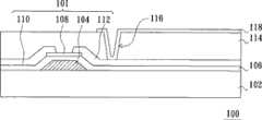
图1为公知有源显示器之单一像素中薄膜晶体管阵列基板的剖面示意图。请参照图1,在薄膜晶体管阵列基板100的制造工艺中,系先在基板102上形成栅极104,接着再形成覆盖住栅极104的栅绝缘层106。之后,在栅绝缘层106上形成非晶硅半导体层(图未示)。由于非晶硅半导体层不透光,为了增加此像素的开口率(aperture rat io),接着必须移除部分的非晶硅半导体层,仅留下位于栅极104上方的部分作为通道层108。FIG. 1 is a schematic cross-sectional view of a thin film transistor array substrate in a single pixel of a known active display. Referring to FIG. 1 , in the manufacturing process of the
之后,于栅绝缘层106上形成源极110与漏极112,以覆盖住部分的通道层108。此时,即大致完成薄膜晶体管101的制作。然后,在基板102上形成具有开口116的保护层114,以暴露出部分的漏极112。并且,在保护层114上形成像素电极118,且像素电极118系填入开口116内而与漏极112电性连接。Afterwards, a
然而,由于非晶硅材料具有光电特性,因此若在反射式显示器中使用薄膜晶体管阵列100,则当环境光从薄膜晶体管101上方入射至通道层108时,会于通道层108内产生漏电流,使得薄膜晶体管阵列100发生不正常作动,导致显示器发生显示异常的问题。However, since the amorphous silicon material has photoelectric properties, if the thin
为解决上述问题,公知系在通道层108上方形成金属遮光层(图未示),以避免环境光照射到通道层108而产生漏电流。但是以此种方式避免薄膜晶体管101产生漏电流,必须在反射式显示器的制造工艺中多加一道光罩,并因此增加反射式显示器的制造工艺成本。To solve the above problems, it is known to form a metal light-shielding layer (not shown) above the
由此可见,上述现有的显示器及其薄膜晶体管阵列基板与薄膜晶体管在产品结构、制造方法(加工方法)与使用上,显然仍存在有不便与缺陷,而亟待加以进一步改进。为了解决上述存在的问题,相关厂商莫不费尽心思来谋求解决之道,但长久以来一直未见适用的设计被发展完成,而一般产品及方法又没有适切的结构及方法能够解决上述问题,此显然是相关业者急欲解决的问题。因此如何能创设一种新的显示器及其薄膜晶体管阵列基板与薄膜晶体管,实属当前重要研发课题之一,亦成为当前业界极需改进的目标。It can be seen that the above-mentioned existing displays and their thin film transistor array substrates and thin film transistors obviously still have inconveniences and defects in product structure, manufacturing method (processing method) and use, and need to be further improved urgently. In order to solve the above-mentioned problems, the relevant manufacturers have tried their best to find a solution, but no suitable design has been developed for a long time, and there is no suitable structure and method for general products and methods to solve the above-mentioned problems. This is obviously a problem that relevant industry players are eager to solve. Therefore, how to create a new display and its thin film transistor array substrate and thin film transistor is one of the current important research and development topics, and it has also become a goal that the industry needs to improve.
发明内容Contents of the invention
本发明的目的在于,克服现有的薄膜晶体管存在的缺陷,而提供一种新的薄膜晶体管,所要解决的技术问题是使其源极与漏极之间的通道层(channel layer)不具光电特性,因而可避免在受光线照射时产生漏电流,非常适于实用。The purpose of the present invention is to overcome the defects of existing thin film transistors and provide a new thin film transistor. The technical problem to be solved is to make the channel layer between the source and drain without photoelectric properties. , so it can avoid leakage current when exposed to light, which is very suitable for practical use.
本发明的另一目的在于,克服现有的薄膜晶体管阵列基板存在的缺陷,而提供一种新的薄膜晶体管阵列基板,所要解决的技术问题是使其可以利用光罩少且成本低的制造工艺制作而成,并具有不因受光照射而产生漏电流的薄膜晶体管,从而更加适于实用。Another object of the present invention is to overcome the defects of existing thin film transistor array substrates and provide a new thin film transistor array substrate. Manufactured, and has a thin film transistor that does not generate leakage current due to light irradiation, so it is more suitable for practical use.
本发明的再一目的在于,克服现有的显示器存在的缺陷,而提供一种新的显示器,所要解决的技术问题是使其薄膜晶体管不会在受光照后产生漏电流,因而可改善其显示效能,从而更加适于实用。Another object of the present invention is to overcome the defects of existing displays and provide a new display. The technical problem to be solved is to make its thin film transistors not generate leakage current after being illuminated, so that the display can be improved. performance, which is more suitable for practical use.
本发明的目的及解决其技术问题是采用以下技术方案来实现的。依据本发明提出的一种薄膜晶体管,其包括栅极、栅绝缘层、源极、漏极及氧化物半导体层。栅极与栅绝缘层分别配置于第一基板上,且栅绝缘层覆盖住栅极。源极与漏极分别配置于栅绝缘层上方。氧化物半导体层共形地配置于源极及漏极上并完全覆盖源极及漏极。氧化物半导体层具有一通道区,通道区位于源极与漏极之间。The purpose of the present invention and the solution to its technical problems are achieved by adopting the following technical solutions. A thin film transistor proposed according to the present invention includes a gate, a gate insulating layer, a source, a drain and an oxide semiconductor layer. The gate and the gate insulating layer are respectively disposed on the first substrate, and the gate insulating layer covers the gate. The source and the drain are respectively arranged above the gate insulating layer. The oxide semiconductor layer is conformally disposed on the source and the drain and completely covers the source and the drain. The oxide semiconductor layer has a channel region, and the channel region is located between the source and the drain.
本发明的目的及解决其技术问题还采用以下技术方案来实现。依据本发明提出的一种薄膜晶体管阵列基板,包括第一基板、多条资料线、多条扫描线、多个上述的薄膜晶体管、保护层与多个像素电极。扫描线与资料线大致上垂直于彼此,而在第一基板上定义出多个像素区域。各薄膜晶体管配置在对应的像素区域内,并且与对应的资料线与扫描线电性连接。保护层覆盖在第一基板上,并且具有暴露出各薄膜晶体管的部分漏极的接触窗开口。这些像素电极分别配置在对应的像素区域内,并填入对应的接触窗开口而与对应的漏极电性连接。The purpose of the present invention and the solution to its technical problem also adopt the following technical solutions to achieve. A thin film transistor array substrate according to the present invention includes a first substrate, a plurality of data lines, a plurality of scanning lines, a plurality of the above thin film transistors, a protection layer and a plurality of pixel electrodes. The scan lines and the data lines are substantially perpendicular to each other, and define a plurality of pixel areas on the first substrate. Each thin film transistor is arranged in a corresponding pixel area, and is electrically connected with a corresponding data line and a scanning line. The protection layer covers the first substrate and has a contact window opening exposing part of the drain of each thin film transistor. The pixel electrodes are respectively arranged in the corresponding pixel regions, and fill the corresponding contact window openings to be electrically connected with the corresponding drain electrodes.
本发明的目的及解决其技术问题另外再采用以下技术方案来实现。依据本发明提出的一种显示器,包括上述的薄膜晶体管阵列基板、透光电极基板以及配置在透光电极基板与薄膜晶体管阵列基板之间的显示介质层。The purpose of the present invention and its technical problems are solved by adopting the following technical solutions in addition. A display according to the present invention includes the above-mentioned thin film transistor array substrate, a light-transmitting electrode substrate, and a display medium layer arranged between the light-transmitting electrode substrate and the thin film transistor array substrate.
本发明的目的及解决其技术问题还可采用以下技术措施进一步实现。The purpose of the present invention and its technical problems can also be further realized by adopting the following technical measures.
在本发明的一实施例中,上述的薄膜晶体管还包括第一欧姆接触层与第二欧姆接触层,其中第一欧姆接触层配置于源极与氧化物半导体层之间,第二欧姆接触层则是配置于漏极与氧化物半导体层之间。In an embodiment of the present invention, the above-mentioned thin film transistor further includes a first ohmic contact layer and a second ohmic contact layer, wherein the first ohmic contact layer is disposed between the source electrode and the oxide semiconductor layer, and the second ohmic contact layer It is disposed between the drain electrode and the oxide semiconductor layer.
借由上述技术方案,本发明显示器及其薄膜晶体管阵列基板与薄膜晶体管至少具有下列优点及有益效果:本发明是以氧化物半导体材料作为显示器的薄膜晶体管的通道层,而由于氧化物半导体不具光电特性,因此可避免薄膜晶体管在照光后产生漏电流的问题。此外,由于氧化物半导体层的材质为可透光材质,因此在本发明的显示器的制造工艺中,可省略氧化物半导体层的图案化制造工艺,以节省制造工艺成本并缩短制造工艺时间。By means of the above technical solution, the display and its thin film transistor array substrate and thin film transistor of the present invention have at least the following advantages and beneficial effects: the present invention uses oxide semiconductor material as the channel layer of the thin film transistor of the display, and since the oxide semiconductor has no photoelectric characteristics, so it can avoid the problem of leakage current of thin film transistors after being illuminated. In addition, since the material of the oxide semiconductor layer is a light-transmitting material, in the manufacturing process of the display of the present invention, the patterning manufacturing process of the oxide semiconductor layer can be omitted, so as to save the manufacturing process cost and shorten the manufacturing process time.
综上所述,本发明是有关于一种显示器及其薄膜晶体管阵列基板与薄膜晶体管。该显示器,包括薄膜晶体管阵列基板、透光电极基板及配置于两者之间的显示介质层。薄膜晶体管阵列基板包括多个具有氧化物半导体层的薄膜晶体管,其中薄膜晶体管的栅极与栅绝缘层分别配置于基板上,且栅绝缘层覆盖住栅极。氧化物半导体层共形地覆盖于栅绝缘层上,并具有位在栅极上方的通道区。薄膜晶体管的源极与漏极分别配置于氧化物半导体层上,并位于通道区的两侧。由于氧化物半导体层的材质为可透光材质,因此在此显示器的制造工艺中,可省略氧化物半导体层的图案化制造工艺,以节省制造工艺成本并缩短制造工艺时间。本发明在技术上有显著的进步,并具有明显的积极效果,诚为一新颖、进步、实用的新设计。To sum up, the present invention relates to a display and its thin film transistor array substrate and thin film transistor. The display includes a thin film transistor array substrate, a light-transmitting electrode substrate and a display medium layer arranged between them. The thin film transistor array substrate includes a plurality of thin film transistors with oxide semiconductor layers, wherein gates and gate insulation layers of the thin film transistors are respectively arranged on the substrate, and the gate insulation layer covers the gates. The oxide semiconductor layer conformally covers the gate insulation layer and has a channel region above the gate. The source and the drain of the thin film transistor are respectively arranged on the oxide semiconductor layer and located at two sides of the channel region. Since the material of the oxide semiconductor layer is a light-transmitting material, in the manufacturing process of the display, the patterning manufacturing process of the oxide semiconductor layer can be omitted, so as to save the manufacturing process cost and shorten the manufacturing process time. The present invention has significant progress in technology, and has obvious positive effects, and is a novel, progressive and practical new design.
上述说明仅是本发明技术方案的概述,为了能够更清楚了解本发明的技术手段,而可依照说明书的内容予以实施,并且为了让本发明的上述和其他目的、特征和优点能够更明显易懂,以下特举较佳实施例,并配合附图,详细说明如下。The above description is only an overview of the technical solution of the present invention. In order to better understand the technical means of the present invention, it can be implemented according to the contents of the description, and in order to make the above and other purposes, features and advantages of the present invention more obvious and understandable , the following preferred embodiments are specifically cited, and in conjunction with the accompanying drawings, the detailed description is as follows.
附图说明Description of drawings
图1为公知有源显示器的单一像素中薄膜晶体管阵列基板的剖面示意图。FIG. 1 is a schematic cross-sectional view of a thin film transistor array substrate in a single pixel of a known active display.
图2为本发明的一实施例中显示器的剖面示意图。FIG. 2 is a schematic cross-sectional view of a display in an embodiment of the present invention.
图3为本发明的另一实施例中显示器的剖面示意图。FIG. 3 is a schematic cross-sectional view of a display in another embodiment of the present invention.
图4为本发明的一实施例中薄膜晶体管阵列基板的示意图。FIG. 4 is a schematic diagram of a thin film transistor array substrate in an embodiment of the present invention.
图5为图4的薄膜晶体管阵列基板在一实施例中的局部剖面示意图。FIG. 5 is a schematic partial cross-sectional view of the thin film transistor array substrate in FIG. 4 in an embodiment.
图6为图4的薄膜晶体管阵列基板在另一实施例中的局部剖面示意图。FIG. 6 is a schematic partial cross-sectional view of the thin film transistor array substrate in FIG. 4 in another embodiment.
图7为图4的薄膜晶体管阵列基板在另一实施例中的局部剖面示意图。FIG. 7 is a schematic partial cross-sectional view of the thin film transistor array substrate in FIG. 4 in another embodiment.
100、210:薄膜晶体管阵列基板100, 210: TFT array substrate
101、300:薄膜晶体管101, 300: thin film transistor
102:基板102: Substrate
104、310:栅极104, 310: grid
106、320:栅绝缘层106, 320: gate insulating layer
108:通道层108: Channel layer
110、340:源极110, 340: source
112、350:漏极112, 350: drain
114、214:保护层114, 214: protective layer
116、217:开口116, 217: opening
118、215:像素电极118, 215: Pixel electrodes
200、201:显示器200, 201: display
211:第一基板211: First Substrate
212:资料线212: data line
213:扫描线213: scan line
216:像素区域216: pixel area
220:显示介质层220: display medium layer
230:透光电极基板230: Translucent electrode substrate
232:第二基板232: Second substrate
234:透明电极234: transparent electrode
236:彩色滤光膜236: Color filter film
330:氧化物半导体层330: oxide semiconductor layer
332:通道区332: Passage area
370、380:欧姆接触层370, 380: ohmic contact layer
具体实施方式Detailed ways
为更进一步阐述本发明为达成预定发明目的所采取的技术手段及功效,以下结合附图及较佳实施例,对依据本发明提出的显示器及其薄膜晶体管阵列基板与薄膜晶体管的具体实施方式、结构、方法、步骤、特征及其功效,详细说明如后。In order to further explain the technical means and effects of the present invention to achieve the intended purpose of the invention, the specific implementation methods, Structure, method, step, feature and effect thereof are as follows in detail.
图2为本发明的一实施例中显示器的剖面示意图。请参照图2,显示器200包括薄膜晶体管阵列基板210、显示介质层220及透光电极基板230,其中透光电极基板230是位于薄膜晶体管阵列基板210上方,显示介质层220则是配置于透光电极基板230与薄膜晶体管阵列基板210之间。FIG. 2 is a schematic cross-sectional view of a display in an embodiment of the present invention. Please refer to FIG. 2, the
透光电极基板230包括第二基板232与透明电极234。透明电极234配置于第二基板232上,并位于第二基板232与显示介质层220之间。而且,第二基板232的材质可以是玻璃或塑胶。在本实施例中,第二基板232的材质例如是聚对苯二甲酸乙二醇酯(Polyethylene Terephthalate,PET)、聚萘二甲酸乙二酯(Polyethylene Naphthalate,PEN)或聚甲基丙烯酸甲酯(Polymethacrylate,PMMA)。The
另一方面,显示介质层220可以是微胶囊电泳层(microcapsuleelectrophoretic layer)、微杯电泳层(microcup electrophoretic layer)、胆固醇型液晶层(cholesteric liquid crystal layer)、电湿润层(electro-wetting layer)或粉体移动层(quick response-liquid powderlayer)。On the other hand, the
特别的是,在另一实施例中,透光电极基板230还可以包括彩色滤光膜(color filter film)236,其是配置于透明电极234与第二基板232之间,如图3所示。也就是说,图3所绘示之显示器201为彩色显示器。Particularly, in another embodiment, the
图4为本发明的一实施例中薄膜晶体管阵列基板的示意图。请参照图4,薄膜晶体管阵列基板210包括第一基板211、多条资料线212、多条扫描线213、多个薄膜晶体管300、保护层214与多个像素电极215。其中,第一基板211的材质可以是玻璃或塑胶。在本实施例中,第一基板211的材质例如是与第二基板232的材质相同,如聚对苯二甲酸乙二醇酯、聚萘二甲酸乙二酯或聚甲基丙烯酸甲酯。换言之,图2所绘示的显示器200可以是可挠式显示器。FIG. 4 is a schematic diagram of a thin film transistor array substrate in an embodiment of the present invention. Referring to FIG. 4 , the thin film
这些资料线212是相互平行地配置于第一基板211上,扫描线213则是大致与资料线212垂直地配置在第一基板211上,而与资料线212在第一基板211上定义出多个像素区域216。这些薄膜晶体管300是分别配置在对应的像素区域216内,并与对应的扫描线213及资料线212电性连接。以下将详述本实施例的薄膜晶体管300的结构。These
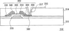
图5为图4的薄膜晶体管阵列基板的局部剖面示意图。请参照图5,薄膜晶体管300包括栅极310、栅绝缘层320、氧化物半导体层330、源极340及漏极350。其中,栅极310与栅绝缘层320分别配置于第一基板211上,且栅绝缘层320覆盖住栅极310。氧化物半导体层330共形地覆盖于栅绝缘层320上,且其具有位在栅极310上方的通道区332。源极340与漏极350分别配置于氧化物半导体330上,并位于通道区332的两侧。请同时参照图4及图5,源极340电性连接至其所对应的资料线212,漏极350则是与配置在像素区域216内的像素电极215(见图4)电性连接。FIG. 5 is a schematic partial cross-sectional view of the thin film transistor array substrate of FIG. 4 . Referring to FIG. 5 , the
栅极310的材质为金属材料或透明导电材料。以本实施例来说,栅极310的材质例如是钼或铬,且其厚度例如是2000埃(angstrom)。栅绝缘层320的材质例如是氧化硅,且其厚度例如是2000埃。氧化物半导体层330的材质例如是铟镓锌氧化物(IGZO)或铟锌氧化物(IZO),且其厚度例如是900埃。源极340与漏极350的材质则可以与栅极310相同或不同,以本实施例来说,源极340与漏极350的材质可以是钼或铬,且其厚度例如是2000埃。The
值得一提的是,为了降低源极340/漏极350与氧化物半导体层330之间的阻抗,在另一实施例中,薄膜晶体管300还可以包括欧姆接触层370与欧姆接触层380,其分别配置于源极340与氧化物半导体层330之间以及漏极350与氧化物半导体层330之间,如图6所示。特别的是,欧姆接触层370与欧姆接触层380的材质可以是导电性高于氧化物半导体层330的铟镓锌氧化物(IGZO)或铟锌氧化物(IZO)。详细来说,在薄膜晶体管300的制造工艺(即制程,以下均称为制造工艺)中,其例如是在单次镀膜制造工艺中,以不同通氧量来同时制成氧化物半导体层330、欧姆接触层370与欧姆接触层380。It is worth mentioning that, in order to reduce the resistance between the
需要注意的是,本发明并不将氧化物半导体层330的位置限定在栅绝缘层320与源极340/漏极350之间,在另一实施例中,源极340与漏极350是配置于栅绝缘层320上,而氧化物半导体层330则是共形地覆盖于源极340与漏极350上,并使其通道区332位在源极340与漏极350之间,如图7所示。由于此实施例先在栅绝缘层320上形成源极340与漏极350,之后再在源极340与漏极350上形成氧化物半导体层330,因此可避免氧化物半导体层330在源极340与漏极350的图案化制造工艺中因蚀刻不当而受损的问题。It should be noted that the present invention does not limit the position of the
而且,在图7所示的实施例中,薄膜晶体管300同样也可以包括前述实施例所述的欧姆接触层370与欧姆接触层380。Moreover, in the embodiment shown in FIG. 7 , the
在前述这些实施例中,由于氧化物半导体层330不具光电特性,因此即使环境光从薄膜晶体管300上方入射至氧化物半导体层330,薄膜晶体管300也不会发生漏电流的问题。特别的是,由于构成氧化物半导体层330的材质可透光,因此在本发明的薄膜晶体管阵列基板210的制造工艺中,不需要移除部分的氧化物半导体层330也不会对其所对应的像素区域内的开口率(aperture ratio)造成影响。换言之,本发明的薄膜晶体管阵列基板210的制造工艺与公知的薄膜晶体管阵列基板100的制造工艺相较之下,不但制造工艺简单且生产成本低。In the above-mentioned embodiments, since the
请再次参照图5,薄膜晶体管阵列基板210中的保护层214是配置于第一基板211上,并具有多个开口217(图中仅绘出一个)。这些开口217是分别对应至各像素区域216,以暴露出其所对应的像素区域216内的薄膜晶体管300的漏极350的一部分。值得一提的是,本实施例的保护层214的材质例如是树脂,而其例如是以自旋涂布(spin coating)的方式形成在第一基板211上,因而具有较佳的平坦化效果。另外,保护层214的厚度约为2.5微米。Referring to FIG. 5 again, the
像素电极215是分别配置在其所对应的像素区域216内,并填入保护层214的开口217内而与漏极350电性连接。在本实施例中,像素电极215的材质例如是铟锌氧化物(ITO)、铟锡氧化物(IZO)或其他的金属导电材料,而其厚度例如是500埃。The
综上所述,本发明具有下列优点:In summary, the present invention has the following advantages:
1.本发明是以氧化物半导体材料作为显示器的薄膜晶体管的通道层,而由于氧化物半导体不具光电特性,因此可避免薄膜晶体管在照光后产生漏电流的问题。1. The present invention uses oxide semiconductor material as the channel layer of the thin film transistor of the display, and since the oxide semiconductor does not have photoelectric properties, the problem of leakage current generated by the thin film transistor after being illuminated can be avoided.
2.由于氧化物半导体层可在室温下成膜,因而能够直接在耐热度不佳的塑胶基板上完成制造工艺。换言之,在具可挠性的显示器的制造工艺中,以具有氧化物半导体层的薄膜晶体管作为驱动元件可简化制造工艺并降低成本。2. Since the oxide semiconductor layer can be formed at room temperature, the manufacturing process can be completed directly on the plastic substrate with poor heat resistance. In other words, in the manufacturing process of the flexible display, using the thin film transistor with the oxide semiconductor layer as the driving element can simplify the manufacturing process and reduce the cost.
3.由于氧化物半导体层的材质为可透光材质,因此在本发明的显示器的制造工艺中,可省略氧化物半导体层的图案化制造工艺,以节省制造工艺成本并缩短制造工艺时间。3. Since the material of the oxide semiconductor layer is a light-transmitting material, in the manufacturing process of the display of the present invention, the patterning manufacturing process of the oxide semiconductor layer can be omitted, so as to save the manufacturing process cost and shorten the manufacturing process time.
4.本发明可利用树脂来作为薄膜晶体管阵列基板上的保护层,因而可获得良好的平坦化效果。4. In the present invention, the resin can be used as the protective layer on the thin film transistor array substrate, so a good planarization effect can be obtained.
以上所述,仅是本发明的较佳实施例而已,并非对本发明作任何形式上的限制,虽然本发明已以较佳实施例揭露如上,然而并非用以限定本发明,任何熟悉本专业的技术人员,在不脱离本发明技术方案范围内,当可利用上述揭示的方法及技术内容作出些许的更动或修饰为等同变化的等效实施例,但凡是未脱离本发明技术方案的内容,依据本发明的技术实质对以上实施例所作的任何简单修改、等同变化与修饰,均仍属于本发明技术方案的范围内。The above description is only a preferred embodiment of the present invention, and does not limit the present invention in any form. Although the present invention has been disclosed as above with preferred embodiments, it is not intended to limit the present invention. Anyone familiar with this field Those skilled in the art, without departing from the scope of the technical solution of the present invention, may use the method and technical content disclosed above to make some changes or modify equivalent embodiments with equivalent changes, but if they do not depart from the content of the technical solution of the present invention, Any simple modifications, equivalent changes and modifications made to the above embodiments according to the technical essence of the present invention still fall within the scope of the technical solution of the present invention.
Claims (6)
Priority Applications (1)
| Application Number | Priority Date | Filing Date | Title |
|---|---|---|---|
| CN200910209686.4ACN102054873B (en) | 2009-11-05 | 2009-11-05 | Display and its thin film transistor array substrate and thin film transistor |
Applications Claiming Priority (1)
| Application Number | Priority Date | Filing Date | Title |
|---|---|---|---|
| CN200910209686.4ACN102054873B (en) | 2009-11-05 | 2009-11-05 | Display and its thin film transistor array substrate and thin film transistor |
Publications (2)
| Publication Number | Publication Date |
|---|---|
| CN102054873A CN102054873A (en) | 2011-05-11 |
| CN102054873Btrue CN102054873B (en) | 2014-03-05 |
Family
ID=43959028
Family Applications (1)
| Application Number | Title | Priority Date | Filing Date |
|---|---|---|---|
| CN200910209686.4AActiveCN102054873B (en) | 2009-11-05 | 2009-11-05 | Display and its thin film transistor array substrate and thin film transistor |
Country Status (1)
| Country | Link |
|---|---|
| CN (1) | CN102054873B (en) |
Families Citing this family (4)
| Publication number | Priority date | Publication date | Assignee | Title |
|---|---|---|---|---|
| TWI499849B (en)* | 2013-03-12 | 2015-09-11 | E Ink Holdings Inc | Pixel structure |
| CN104051472A (en)* | 2014-06-19 | 2014-09-17 | 京东方科技集团股份有限公司 | Display device, array substrate and manufacturing method thereof |
| CN111856832B (en)* | 2019-04-23 | 2024-09-10 | 元太科技工业股份有限公司 | Reflective active element array substrate, manufacturing method thereof and reflective display device |
| TWI702457B (en) | 2019-04-23 | 2020-08-21 | 元太科技工業股份有限公司 | Reflective active device array substrate and manufacturing method thereof and reflective display device and manufacturing method thereof |
Citations (2)
| Publication number | Priority date | Publication date | Assignee | Title |
|---|---|---|---|---|
| CN1892389A (en)* | 2005-07-08 | 2007-01-10 | 阿尔卑斯电气株式会社 | Liquid crystal display device |
| CN101328409A (en)* | 2007-06-22 | 2008-12-24 | 三星电子株式会社 | Oxide-based TFT, zinc oxide-based etchant, and method for forming them |
Family Cites Families (2)
| Publication number | Priority date | Publication date | Assignee | Title |
|---|---|---|---|---|
| CN101577231B (en)* | 2005-11-15 | 2013-01-02 | 株式会社半导体能源研究所 | Semiconductor device and method of manufacturing the same |
| KR20070070382A (en)* | 2005-12-29 | 2007-07-04 | 엘지.필립스 엘시디 주식회사 | Array substrate for liquid crystal display device and manufacturing method thereof |
- 2009
- 2009-11-05CNCN200910209686.4Apatent/CN102054873B/enactiveActive
Patent Citations (2)
| Publication number | Priority date | Publication date | Assignee | Title |
|---|---|---|---|---|
| CN1892389A (en)* | 2005-07-08 | 2007-01-10 | 阿尔卑斯电气株式会社 | Liquid crystal display device |
| CN101328409A (en)* | 2007-06-22 | 2008-12-24 | 三星电子株式会社 | Oxide-based TFT, zinc oxide-based etchant, and method for forming them |
Non-Patent Citations (1)
| Title |
|---|
| JP特开2009-135530A 2009.06.18 |
Also Published As
| Publication number | Publication date |
|---|---|
| CN102054873A (en) | 2011-05-11 |
Similar Documents
| Publication | Publication Date | Title |
|---|---|---|
| TWI553837B (en) | Method of making a display panel | |
| CN102914922B (en) | In-plane switching mode liquid crystal display device | |
| CN105527767A (en) | Array substrate and liquid crystal display | |
| US9070599B2 (en) | Array substrate, manufacturing method thereof and display device | |
| CN105448933B (en) | For the array substrate and preparation method thereof in liquid crystal display panel | |
| CN102064180A (en) | Active element, pixel structure and display panel | |
| US20150380434A1 (en) | Array substrate and a display device | |
| CN106371256A (en) | Pixel structure, display panel and display device | |
| CN115509056A (en) | Array substrate, control method and manufacturing method thereof and electronic paper display device | |
| US20130161612A1 (en) | Display device and image display system employing the same | |
| KR102659970B1 (en) | Display substrate and method of manufacturing the same | |
| CN104698661A (en) | Display panel and method for manufacturing the same | |
| CN102054873B (en) | Display and its thin film transistor array substrate and thin film transistor | |
| CN106298809A (en) | Thin-film transistor array base-plate and preparation method thereof, liquid crystal indicator | |
| TWI467770B (en) | Display and its thin film transistor array substrate and thin film transistor | |
| TW201321874A (en) | Pixel structure and its manufacturing method | |
| KR102484136B1 (en) | Display substrate, liquid crystal display comprising the same, and manufacturing method the same | |
| KR20110074242A (en) | Electrophoretic display device and manufacturing method thereof | |
| CN103543566B (en) | Pixel structure and manufacturing method thereof | |
| CN102890373A (en) | In-plane switching liquid crystal display panel and method of manufacturing the same | |
| CN110993696B (en) | Semiconductor device with a semiconductor device having a plurality of semiconductor chips | |
| CN108388057B (en) | Array substrate | |
| CN102819133B (en) | Transflective liquid crystal display array substrate, manufacturing method and liquid crystal display screen | |
| US8456582B2 (en) | Active device, pixel structure and display panel | |
| CN115202126A (en) | Array substrate and electronic paper display device |
Legal Events
| Date | Code | Title | Description |
|---|---|---|---|
| C06 | Publication | ||
| PB01 | Publication | ||
| C10 | Entry into substantive examination | ||
| SE01 | Entry into force of request for substantive examination | ||
| GR01 | Patent grant | ||
| GR01 | Patent grant |